1. Product profile 1.1 General description 10 W LDMOS power transistor for applications at frequencies from HF to 2200 MHz [1] Test signal: 3GPP; test model 1; 64 DPCH; PAR = 7.5 dB at 0.01 % probability on CCDF per carrier; carrier spacing 5 MHz. 1.2 Features and benefits Easy power control Integrated ESD protection Excellent ruggedness High efficiency Excellent thermal stability No internal matching for broadband operation Compliant to Directive 2002/95/EC, regarding Restriction of Hazardous Substances (RoHS) 1.3 Applications RF power amplifiers for applications in the HF to 2200 MHz frequency range Broadcast drivers BLF640 Broadband power LDMOS transistor Rev. 3 — 1 September 2015 Product data sheet Table 1. Typical performance I Dq = 100 mA; T case = 25 C in a common source class-AB production test circuit. Test signal f V DS P L(AV) G p D ACPR (MHz) (V) (W) (dB) (%) (dBc) 2-carrier W-CDMA 2110 to 2170 28 0.7 18.5 15 50 [1] 1-carrier W-CDMA 2110 to 2170 28 2 19.3 31 39 [1]
Transcript
1. Product profile
1.1 General description
10 W LDMOS power transistor for applications at frequencies from HF to 2200 MHz
[1] Test signal: 3GPP; test model 1; 64 DPCH; PAR = 7.5 dB at 0.01 % probability on CCDF per carrier; carrier spacing 5 MHz.
1.2 Features and benefits
Easy power control
Integrated ESD protection
Excellent ruggedness
High efficiency
Excellent thermal stability
No internal matching for broadband operation
Compliant to Directive 2002/95/EC, regarding Restriction of Hazardous Substances (RoHS)
1.3 Applications
RF power amplifiers for applications in the HF to 2200 MHz frequency range
Broadcast drivers
BLF640Broadband power LDMOS transistorRev. 3 — 1 September 2015 Product data sheet
Table 1. Typical performanceIDq = 100 mA; Tcase = 25 C in a common source class-AB production test circuit.
Product data sheet Rev. 3 — 1 September 2015 2 of 12
BLF640Broadband power LDMOS transistor
6. Characteristics
7. Test information
7.1 Ruggedness in class-AB operation
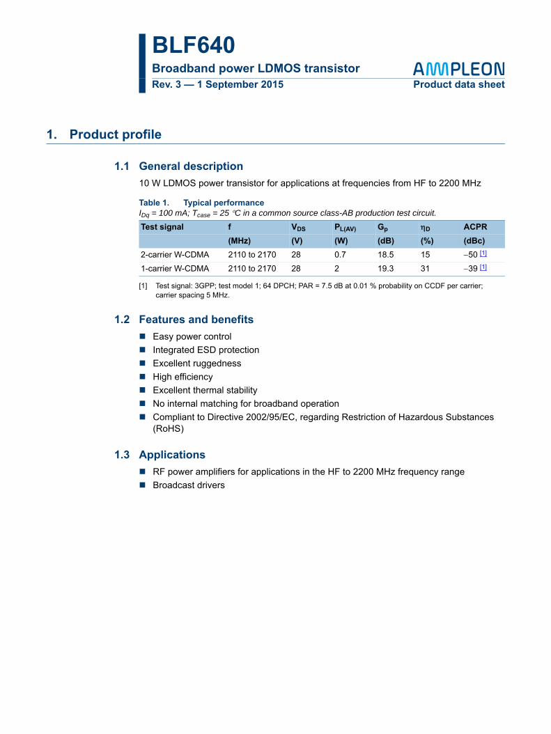
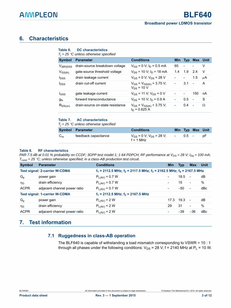
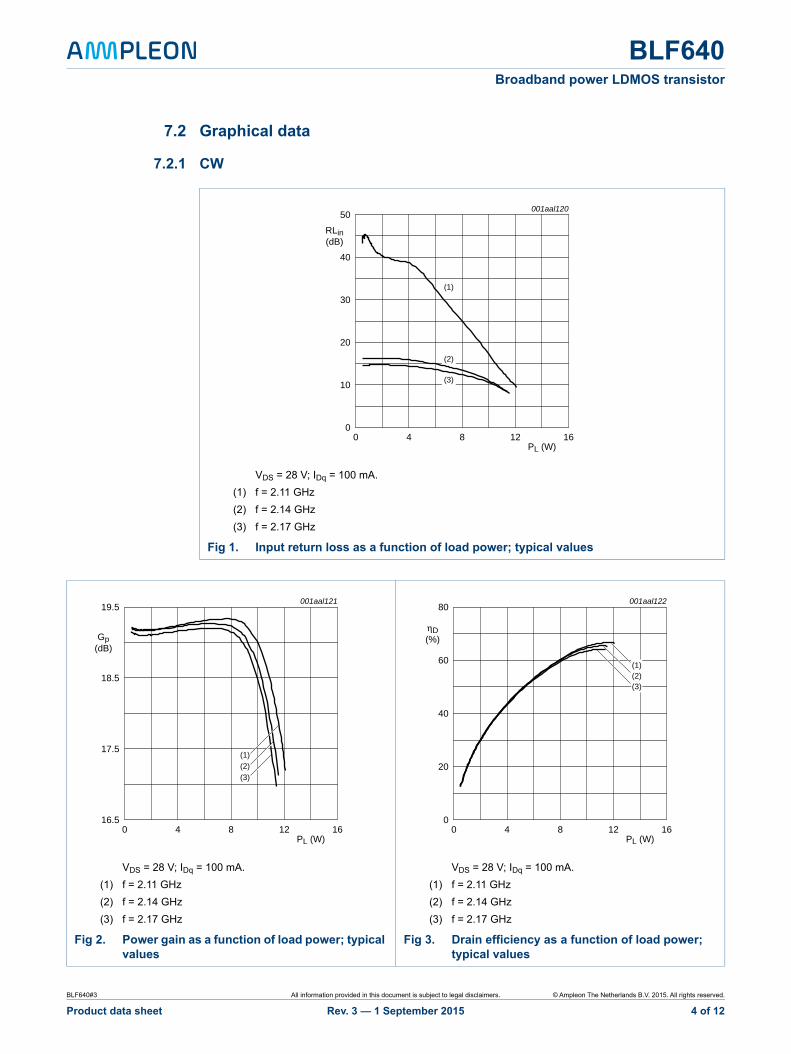
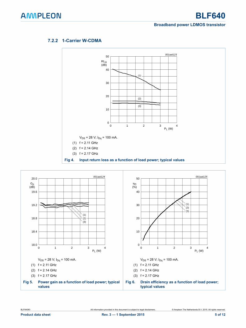
The BLF640 is capable of withstanding a load mismatch corresponding to VSWR = 10 : 1 through all phases under the following conditions: VDS = 28 V; f = 2140 MHz at PL = 10 W.
Table 6. DC characteristicsTj = 25 C unless otherwise specified
Symbol Parameter Conditions Min Typ Max Unit
V(BR)DSS drain-source breakdown voltage VGS = 0 V; ID = 0.5 mA 65 - - V
VGS(th) gate-source threshold voltage VDS = 10 V; ID = 18 mA 1.4 1.9 2.4 V
IDSS drain leakage current VGS = 0 V; VDS = 28 V - - 1.5 A
IDSX drain cut-off current VGS = VGS(th) + 3.75 V; VDS = 10 V
- 3.1 - A
IGSS gate leakage current VGS = 11 V; VDS = 0 V - - 150 nA
gfs forward transconductance VDS = 10 V; ID = 0.9 A - 0.5 - S
RDS(on) drain-source on-state resistance VGS = VGS(th) + 3.75 V; ID = 0.625 A
- 0.4 -
Table 7. AC characteristicsTj = 25 C unless otherwise specified
Table 8. RF characteristicsPAR 7.5 dB at 0.01 % probability on CCDF; 3GPP test model 1; 1-64 PDPCH; RF performance at VDS = 28 V; IDq = 100 mA; Tcase = 25 C; unless otherwise specified; in a class-AB production test circuit.
Symbol Parameter Conditions Min Typ Max Unit
Test signal: 2-carrier W-CDMA f1 = 2112.5 MHz; f2 = 2117.5 MHz; f3 = 2162.5 MHz; f4 = 2167.5 MHz
Gp power gain PL(AV) = 0.7 W - 18.5 - dB
D drain efficiency PL(AV) = 0.7 W - 15 - %
ACPR adjacent channel power ratio PL(AV) = 0.7 W - 50 - dBc
Test signal: 1-carrier W-CDMA f1 = 2112.5 MHz; f2 = 2167.5 MHz
Gp power gain PL(AV) = 2 W 17.3 19.3 - dB
D drain efficiency PL(AV) = 2 W 29 31 - %
ACPR adjacent channel power ratio PL(AV) = 2 W - 39 36 dBc
Product data sheet Rev. 3 — 1 September 2015 9 of 12
BLF640Broadband power LDMOS transistor
12. Legal information
12.1 Data sheet status
[1] Please consult the most recently issued document before initiating or completing a design.
[2] The term ‘short data sheet’ is explained in section “Definitions”.
[3] The product status of device(s) described in this document may have changed since this document was published and may differ in case of multiple devices. The latest product status information is available on the Internet at URL http://www.ampleon.com.
12.2 Definitions
Draft — The document is a draft version only. The content is still under internal review and subject to formal approval, which may result in modifications or additions. Ampleon does not give any representations or warranties as to the accuracy or completeness of information included herein and shall have no liability for the consequences of use of such information.
Short data sheet — A short data sheet is an extract from a full data sheet with the same product type number(s) and title. A short data sheet is intended for quick reference only and should not be relied upon to contain detailed and full information. For detailed and full information see the relevant full data sheet, which is available on request via the local Ampleon sales office. In case of any inconsistency or conflict with the short data sheet, the full data sheet shall prevail.
Product specification — The information and data provided in a Product data sheet shall define the specification of the product as agreed between Ampleon and its customer, unless Ampleon and customer have explicitly agreed otherwise in writing. In no event however, shall an agreement be valid in which the Ampleon product is deemed to offer functions and qualities beyond those described in the Product data sheet.
12.3 Disclaimers
Limited warranty and liability — Information in this document is believed to be accurate and reliable. However, Ampleon does not give any representations or warranties, expressed or implied, as to the accuracy or completeness of such information and shall have no liability for the consequences of use of such information. Ampleon takes no responsibility for the content in this document if provided by an information source outside of Ampleon.
In no event shall Ampleon be liable for any indirect, incidental, punitive, special or consequential damages (including - without limitation - lost profits, lost savings, business interruption, costs related to the removal or replacement of any products or rework charges) whether or not such damages are based on tort (including negligence), warranty, breach of contract or any other legal theory.
Notwithstanding any damages that customer might incur for any reason whatsoever, Ampleon’ aggregate and cumulative liability towards customer for the products described herein shall be limited in accordance with the Terms and conditions of commercial sale of Ampleon.
Right to make changes — Ampleon reserves the right to make changes to information published in this document, including without limitation specifications and product descriptions, at any time and without notice. This document supersedes and replaces all information supplied prior to the publication hereof.
Suitability for use — Ampleon products are not designed, authorized or warranted to be suitable for use in life support, life-critical or safety-critical systems or equipment, nor in applications where failure or malfunction of an
Ampleon product can reasonably be expected to result in personal injury, death or severe property or environmental damage. Ampleon and its suppliers accept no liability for inclusion and/or use of Ampleon products in such equipment or applications and therefore such inclusion and/or use is at the customer’s own risk.
Applications — Applications that are described herein for any of these products are for illustrative purposes only. Ampleon makes no representation or warranty that such applications will be suitable for the specified use without further testing or modification.
Customers are responsible for the design and operation of their applications and products using Ampleon products, and Ampleon accepts no liability for any assistance with applications or customer product design. It is customer’s sole responsibility to determine whether the Ampleon product is suitable and fit for the customer’s applications and products planned, as well as for the planned application and use of customer’s third party customer(s). Customers should provide appropriate design and operating safeguards to minimize the risks associated with their applications and products.
Ampleon does not accept any liability related to any default, damage, costs or problem which is based on any weakness or default in the customer’s applications or products, or the application or use by customer’s third party customer(s). Customer is responsible for doing all necessary testing for the customer’s applications and products using Ampleon products in order to avoid a default of the applications and the products or of the application or use by customer’s third party customer(s). Ampleon does not accept any liability in this respect.
Limiting values — Stress above one or more limiting values (as defined in the Absolute Maximum Ratings System of IEC 60134) will cause permanent damage to the device. Limiting values are stress ratings only and (proper) operation of the device at these or any other conditions above those given in the Recommended operating conditions section (if present) or the Characteristics sections of this document is not warranted. Constant or repeated exposure to limiting values will permanently and irreversibly affect the quality and reliability of the device.
Terms and conditions of commercial sale — Ampleon products are sold subject to the general terms and conditions of commercial sale, as published at http://www.ampleon.com/terms, unless otherwise agreed in a valid written individual agreement. In case an individual agreement is concluded only the terms and conditions of the respective agreement shall apply. Ampleon hereby expressly objects to applying the customer’s general terms and conditions with regard to the purchase of Ampleon products by customer.
No offer to sell or license — Nothing in this document may be interpreted or construed as an offer to sell products that is open for acceptance or the grant, conveyance or implication of any license under any copyrights, patents or other industrial or intellectual property rights.
Export control — This document as well as the item(s) described herein may be subject to export control regulations. Export might require a prior authorization from competent authorities.
Non-automotive qualified products — Unless this data sheet expressly states that this specific Ampleon product is automotive qualified, the product is not suitable for automotive use. It is neither qualified nor tested in accordance with automotive testing or application requirements. Ampleon accepts no liability for inclusion and/or use of non-automotive qualified products in automotive equipment or applications.
In the event that customer uses the product for design-in and use in automotive applications to automotive specifications and standards, customer (a) shall use the product without Ampleon’ warranty of the product for such automotive applications, use and specifications, and (b) whenever customer uses the product for automotive applications beyond Ampleon’ specifications such use shall be solely at customer’s own risk, and (c) customer fully indemnifies Ampleon for any liability, damages or failed product claims resulting from customer design and use of the product for automotive applications beyond Ampleon’ standard warranty and Ampleon’ product specifications.
Translations — A non-English (translated) version of a document is for reference only. The English version shall prevail in case of any discrepancy between the translated and English versions.
12.4 TrademarksNotice: All referenced brands, product names, service names and trademarks are the property of their respective owners.
Any reference or use of any ‘NXP’ trademark in this document or in or on the surface of Ampleon products does not result in any claim, liability or entitlement vis-à-vis the owner of this trademark. Ampleon is no longer part of the NXP group of companies and any reference to or use of the ‘NXP’ trademarks will be replaced by reference to or use of Ampleon’s own Any reference or use of any ‘NXP’ trademark in this document or in or on the surface of Ampleon products does not result in any claim, liability or entitlement vis-à-vis the owner of this trademark. Ampleon is no longer part of the NXP group of companies and any reference to or use of the ‘NXP’ trademarks will be replaced by reference to or use of Ampleon’s own trademarks.
13. Contact information
For more information, please visit: http://www.ampleon.com
For sales office addresses, please visit: http://www.ampleon.com/sales


![BLF188XRG - Ampleon · Power LDMOS transistor 2. Pinning information Table 2. Pinning [1] Connected to flange. 3. Ordering information Table 3. Ordering information 4. Limiting values](https://static.documents.pub/doc/80x56/5eb8697419ced03315371e1c/blf188xrg-ampleon-power-ldmos-transistor-2-pinning-information-table-2-pinning.jpg)


