VLSI Made Easy: VLSI Interview Questions file:///C|/Users/COMSOL/Desktop/blog-page.html[6/21/2014 7:58:13 PM] A unique blog which will give you the great interaction to the most advanced enhancements to the new technical trends in Very Large Scale Integration industry. The main aim of this blog is to bring you the all available materials, books related to VLSI which would help mostly VLSI Students VLSI Made Easy Home eBooks VLSI Interview Questions Different File Formats (file extensions) VLSI Interview Questions VLSI FAQs 1. What is metastability? When setup or hold window is violated in an flip flop then signal attains a unpredictable value or state known as metastability. 2. What is MTBF? What it signifies? MTBF-Mean Time Before Failure Average time to next failure 3. How chance of metastable state failure can be reduced? Lowering clock frequency Lowering data speed Using faster flip flop 4. What are the advantages of using synchronous reset ? No metastability problem with synchronous reset (provided recovery and removal time for reset is taken care). Simulation of synchronous reset is easy. 5. What are the disadvantages of using synchronous reset ? Synchronous reset is slow. Implementation of synchronous reset requires more number of gates compared to asynchronous reset design. An active clock is essential for a synchronous reset design. Hence you can expect more power consumption. 6. What are the advantages of using asynchronous reset ? Implementation of asynchronous reset requires less number of gates compared to synchronous reset design. Asynchronous reset is fast. Clocking scheme is not necessary for an asynchronous design. Hence design consumes less power. Asynchronous design style is also one of the latest design options to achieve low power. Design community is scrathing their head over asynchronous design possibilities. 7. What are the disadvantages of using asynchronous reset ? Metastability problems are main concerns of asynchronous reset scheme (design). Static timing analysis and DFT becomes difficult due to asynchronous reset. 8. What are the 3 fundamental operating conditions that determine the delay characteristics of gate? How operating 1 Search This Blog Analog Design (2) ASIC Design (2) BOOKS (1) Digital Design (3) Low Power Design (1) Physical Design (4) STA (1) Labels 0 More Next Blog» Create Blog Sign In
A unique blog which will give you the great interaction to the most advanced enhancements to the new technical trends in Very Large Scale Integrationindustry. The main aim of this blog is to bring you the all available materials, books related to VLSI which would help mostly VLSI Students
VLSI Made Easy
Home eBooks VLSI Interview Questions Different File Formats (file extensions)
VLSI Interview Questions
VLSI FAQs1. What is metastability?
When setup or hold window is violated in an flip flop then signal attains a unpredictable value or state known asmetastability.
2. What is MTBF? What it signifies?
MTBF-Mean Time Before Failure
Average time to next failure
3. How chance of metastable state failure can be reduced?
Lowering clock frequencyLowering data speedUsing faster flip flop
4. What are the advantages of using synchronous reset ?
No metastability problem with synchronous reset (provided recovery and removal time for reset is taken care).
Simulation of synchronous reset is easy.
5. What are the disadvantages of using synchronous reset ?
Synchronous reset is slow.
Implementation of synchronous reset requires more number of gates compared to asynchronous reset design.
An active clock is essential for a synchronous reset design. Hence you can expect more power consumption.
6. What are the advantages of using asynchronous reset ?
Implementation of asynchronous reset requires less number of gates compared to synchronous reset design.
Asynchronous reset is fast.
Clocking scheme is not necessary for an asynchronous design. Hence design consumes less power. Asynchronousdesign style is also one of the latest design options to achieve low power. Design community is scrathing their headover asynchronous design possibilities.
7. What are the disadvantages of using asynchronous reset ?
Metastability problems are main concerns of asynchronous reset scheme (design).
Static timing analysis and DFT becomes difficult due to asynchronous reset.
8. What are the 3 fundamental operating conditions that determine the delay characteristics of gate? How operating
a. Increase in metal width b. Increase in metal length c. Decrease in metal length d. Lot of metal layers
16) The minimum height and width a cell can occupy in the design is called as ___.
a. Unit Tile cell b. Multi heighten cell c. LVT cell d. HVT cell
17) CRPR stands for ___.
a. Cell Convergence Pessimism Removal b. Cell Convergence Preset Removal c. Clock Convergence Pessimism Removal d. ClockConvergence Preset Removal
18) In OCV timing check, for setup time, ___.
a. Max delay is used for launch path and Min delay for capture path b. Min delay is used for launch path and Max delay forcapture path c. Both Max delay is used for launch and Capture path d. Both Min delay is used for both Capture and Launch paths
19) "Total metal area and(or) perimeter of conducting layer / gate to gate area" is called ___.
a. Utilization b. Aspect Ratio c. OCV d. Antenna Ratio
20) The Solution for Antenna effect is ___.
a. Diode insertion b. Shielding c. Buffer insertion d. Double spacing
21) To avoid cross talk, the shielded net is usually connected to ___.
a. VDD b. VSS c. Both VDD and VSS d. Clock
22) If the data is faster than the clock in Reg to Reg path ___ violation may come.
a. Setup b. Hold c. Both d. None
23) Hold violations are preferred to fix ___.
a. Before placement b. After placement c. Before CTS d. After CTS
24) Which of the following is not present in SDC ___?
a. Max tran b. Max cap c. Max fanout d. Max current density
25) Timing sanity check means (with respect to PD)___.
a. Checking timing of routed design with out net delays b. Checking Timing of placed design with net delays c. Checking Timingof unplaced design without net delays d. Checking Timing of routed design with net delays
26) Which of the following is having highest priority at final stage (post routed) of the design ___?
a. Setup violation b. Hold violation c. Skew d. None
27) Which of the following is best suited for CTS?
a. CLKBUF b. BUF c. INV d. CLKINV
28) Max voltage drop will be there at(with out macros) ___.
a. Left and Right sides b. Bottom and Top sides c. Middle d. None
29) Which of the following is preferred while placing macros ___?
a. Macros placed center of the die b. Macros placed left and right side of die c. Macros placed bottom and top sides of die d.Macros placed based on connectivity of the I/O
30) Routing congestion can be avoided by ___.
a. placing cells closer b. Placing cells at corners c. Distributing cells d. None
31) Pitch of the wire is ___.
a. Min width b. Min spacing c. Min width - min spacing d. Min width + min spacing
32) In Physical Design following step is not there ___.
a. Floorplaning b. Placement c. Design Synthesis d. CTS
33) In technology file if 7 metals are there then which metals you will use for power?
a. Metal1 and metal2 b. Metal3 and metal4 c. Metal5 and metal6 d. Metal6 and metal7
34) If metal6 and metal7 are used for the power in 7 metal layer process design then which metals you willuse for clock ?
a. Metal1 and metal2 b. Metal3 and metal4 c. Metal4 and metal5 d. Metal6 and metal7
35) In a reg to reg timing path Tclocktoq delay is 0.5ns and TCombodelay is 5ns and Tsetup is 0.5ns then the
36) Difference between Clock buff/inverters and normal buff/inverters is __.
a. Clock buff/inverters are faster than normal buff/inverters b. Clock buff/inverters are slower than normal buff/inverters c. Clockbuff/inverters are having equal rise and fall times with high drive strengths compare to normal buff/inverters d. Normalbuff/inverters are having equal rise and fall times with high drive strengths compare to Clock buff/inverters.
37) Which configuration is more preferred during floorplaning ?
a. Double back with flipped rows b. Double back with non flipped rows c. With channel spacing between rows and no double backd. With channel spacing between rows and double back
38) What is the effect of high drive strength buffer when added in long net?
a. Delay on the net increases b. Capacitance on the net increases c. Delay on the net decreases d. Resistance on the netincreases.
39) Delay of a cell depends on which factors ?
a. Output transition and input load b. Input transition and Output load c. Input transition and Output transition d. Input load andOutput Load.
40) After the final routing the violations in the design ___.
a. There can be no setup, no hold violations b. There can be only setup violation but no hold c. There can be only hold violationnot Setup violation d. There can be both violations.
41) Utilisation of the chip after placement optimisation will be ___.
a. Constant b. Decrease c. Increase d. None of the above
42) What is routing congestion in the design?
a. Ratio of required routing tracks to available routing tracks b. Ratio of available routing tracks to required routing tracks c.Depends on the routing layers available d. None of the above
43) What are preroutes in your design?
a. Power routing b. Signal routing c. Power and Signal routing d. None of the above.
44) Clock tree doesn't contain following cell ___.
a. Clock buffer b. Clock Inverter c. AOI cell d. None of the above
Below are the important VLSI CMOS interview questions. This set of interview questions may be updated in future. Answers will
be posted one by one as and when i prepare them ! Readers are encouraged to post answers in comment section. Here we
go.........· Draw Vds-Ids curve for an MOSFET. How it varies with a) increasing Vgs b)velocity saturation c)Channel length modulationd)W/L ratio.· What is body effect? Write mathematical expression? Is it due to parallel or serial connection of MOSFETs?· What is latch-up in CMOS design and what are the ways to prevent it?· What is Noise Margin? Explain with the help of Inverter.· What happens to delay if you increase load capacitance?· Give the various techniques you know to minimize power consumption for CMOS logic?· What happens when the PMOS and NMOS are interchanged with one another in an inverter?· What is body effect?· Why is NAND gate preferred over NOR gate for fabrication?· What is Noise Margin? Explain the procedure to determine Noise Margin· Explain sizing of the inverter?· How do you size NMOS and PMOS transistors to increase the threshold voltage?· What happens to delay if we include a resistance at the output of a CMOS circuit?· What are the limitations in increasing the power supply to reduce delay?· How does Resistance of the metal lines vary with increasing thickness and increasing length?
· What is Charge Sharing? Explain the Charge Sharing problem while sampling data from a Bus?· Why do we gradually increase the size of inverters in buffer design? Why not give the output of a circuit to one large inverter?· Give the expression for CMOS switching power dissipation?· Why is the substrate in NMOS connected to ground and in PMOS to VDD?· What is the fundamental difference between a MOSFET and BJT ?· Which transistor has higher gain- BJT or MOS and why?· Why PMOS and NMOS are sized equally in a Transmission Gates?· What is metastability? When/why it will occur? What are the different ways to avoid this?· Explain zener breakdown and avalanche breakdown?* What happens if Vds is increased over saturation?· In the I-V characteristics curve, why is the saturation curve flat or constant? · What happens if a resistor is added in series with the drain in a CMOS transistor?· What are the different regions of operation in a CMOS transistor?· What are the effects of the output characteristics for a change in the beta (β) value?· What is the effect of body bias?· What is hot electron effect and how can it be eliminated?· What is channel length modulation?· What is the effect of temperature on threshold voltage?· What is the effect of temperature on mobility?· What is the effect of gate voltage on mobility?· What are the different types of scaling?· What is stage ratio?· What is charge sharing on a bus?· What is electron migration and how can it be eliminated?· Can both PMOS and NMOS transistors pass good 1 and good 0? Explain.· Why is only NMOS used in pass transistor logic?· What are the different methodologies used to reduce the charge sharing in dynamic logic?· What are setup and hold time violations? How can they be eliminated?· Explain the operation of basic SRAM and DRAM.· Which ones take more time in SRAM: Read operation or Write operation? Why?· What is meant by clock race?· What is meant by single phase and double phase clocking?· If given a choice between NAND and NOR gates, which one would you pick? Explain.· Explain the origin of the various capacitances in the CMOS transistor and the physical reasoning behind it.· Why should the number of CMOS transistors that are connected in series be reduced?· What is charge sharing between bus and memory element?· What is crosstalk and how can it be avoided?· Realize an XOR gate using NAND gate.· What are the advantages and disadvantages of Bi-CMOS process?· Draw an XOR gate with using minimum number of transistors and explain the operation.· What are the critical parameters in a latch and flip-flop?· What is the significance of sense amplifier in an SRAM?· Explain Domino logic.· What are the advantages of depletion mode devices over the enhancement mode devices?· How can the rise and fall times in an inverter be equated?· What is meant by leakage current?· Realize an OR gate using NAND gate.· Realize an NAND gate using a 2:1 multiplexer.· Realize an NOR gate using a 2:1 multiplexer.· Draw the layout of a simple inverter.· What are the substrates of PMOS and NMOS transistors connected to and explain the results if the connections areinterchanged with the other.· What are repeaters?· What is tunneling problem?· What is meant by negative biased instability and how can it be avoided?· What is Elmore delay algorithm?· What is meant by metastability?· What is the effect of Vdd on delay?
· What is the effect of delay, rise and fall times with increase in load capacitance?· What is the value of mobility of electrons?· What is value of mobility of holes?· Give insights of an inverter. Draw Layout. Explain the working.* Give insights of a 2 input NOR gate. Draw Layout. Explain the working.· Give insights of a 2 input NAND gate. Draw layout. Explain the working?· Implement F= not (AB+CD) using CMOS gates.· What is a pass gate. Explain the working?· Why do we need both PMOS and NMOS transistors to implement a pass gate?· What does the above code synthesize to?· Draw cross section of a PMOS transistor.· Draw cross section of an NMOS transistor.· What is a D-latch?· Implement D flip-flop with a couple of latches?· Implement a 2 input AND gate using transmission gate?· Explain various adders and difference between them?· How can you construct both PMOS and NMOS on a single substrate?· What happens when the gate oxide is very thin?· What is SPICE?· What are the differences between IRSIM and SPICE?· What are the differences between netlist of HSPICE and Spectre?· Implement F = AB+C using CMOS gates?· What is hot electron effect?· Define threshold voltage?· List out the factors affecting power consumption on a chip?· What r the phenomenon which come into play when the devices are scaled to the sub-micron lengths?· What is clock feed through?· Implement an Inverter using a single transistor?· What is Fowler-Nordheim Tunneling?· Which gate is normally preferred while implementing circuits using CMOS logic, NAND or NOR? Why?· Draw the Differential Sense Amplifier and explain its working. How to size this circuit?· What happens if we use an Inverter instead of the Differential Sense Amplifier?· Draw the SRAM Write Circuitry· How did you arrive at sizes of transistor in SRAM?· How does the size of PMOS pull up transistors for bit and bitbar lines affect SRAM’s performance?· What is the critical path in a SRAM?· Draw the timing diagram for a SRAM Read. What happens if we delay the enabling of Clock signal?· Give a big picture of the entire SRAM layout showing placements of SRAM cells, row decoders, column decoders, read circuit,write circuit and buffers.· In a SRAM layout, which metal layers would you prefer for Word Lines and Bit Lines? Why?
Design For Test-DFT
Answer:For designs with both positive and negative clocked flops, the scan insertion tool will always route the scan chain so that thenegative clocked flops come before the positive edge flops in the chain. This avoids the need of lockup latch.For the same clock domain the negedge flops will always capture the data just captured into the posedge flops on the posedge ofthe clock.For the multiple clock domains, it all depends upon how the clock trees are balanced. If the clock domains are completelyasynchronous, ATPG has to mask the receiving flops.
Answer1:Based on timing and congestion the tool optimally places standard cells. While doing so, if scan chains are detached, it can breakthe chain ordering (which is done by a scan insertion tool like DFT compiler from Synopsis and can reorder to optimize it.... itmaintains the number of flops in a chain.
In scan chains if some flip flops are +ve edge triggered and remaining flip flops are -ve edge triggered how it behaves?
Answer2:During placement, the optimization may make the scan chain difficult to route due to congestion. Hence the tool will re-orderthe chain to reduce congestion.This sometimes increases hold time problems in the chain. To overcome these buffers may have to be inserted into the scanpath. It may not be able to maintain the scan chain length exactly. It cannot swap cell from different clock domains.Because of scan chain reordering patterns generated earlier is of no use. But this is not a problem as ATPG can be redone byreading the new net list.what are the differences between SIMULATION and SYNTHESIS
Simulation <= verify your design.
synthesis <= Check for your timing
Simulation is used to verify the functionality of the circuit.. a)Functional Simulation:study of ckt's operation independent of timing
parameters and gate delays. b) Timing Simulation :study including estimated delays, verify setup,hold and other timing
requirements of devices like flip flops are met.
Synthesis:One of the foremost in back end steps where by synthesizing is nothing but converting VHDL or VERILOG description
to a set of primitives(equations as in CPLD) or components(as in FPGA'S)to fit into the target technology.Basically the synthesis
tools convert the design description into equations or components
Can u tell me the differences between latches & flipflops?
There are 2 types of circuits:
1. Combinational
2. Sequential
Latches and flipflops both come under the category of "sequential circuits", whose output depends not only on the current inputs,
but also on previous inputs and outputs. Difference: Latches are level-sensitive, whereas, FF are edge sensitive. By edge
sensitive, I mean O/p changes only when there is a clock transition.( from 1 to 0, or from 0 to 1)
Example: In a flipflop, inputs have arrived on the input lines at time= 2 seconds. But, output won't change immediately. At time
= 3 seconds, clock transition takes place. After that, O/P will change.
Flip-flops are of 2 types:
1.Positive edge triggered
2. negative edge triggered
1)fllipflops take twice the nymber of gates as latches
2) so automatically delay is more for flipflops
3)power consumption is also more
latch does not have a clock signal, whereas a flip-flop always does.
What is slack?
The slack is the time delay difference from the expected delay(1/clock) to the actual delay in a particular path.
Slack may be +ve or -ve.
Equivalence between VHDL and C?
There is concept of understanding in C there is structure.Based upon requirement structure provide facility to store collection of
different data types.
In VHDL we have direct access to memory so instead of using pointer in C (and member of structure) we can write interface
store data in memory and access it.
RTL and Behavioral
Register transfer language means there should be data flow between two registers and logic is in between them for end registers
data should flow.
Behavioral means how hardware behave determine the exact way it works we write using HDL syntax.For complex projects it is
20. Draw the stick diagram of a NOR gate. Optimize it
21. For CMOS logic, give the various techniques you know to minimize power consumption
22. What is Charge Sharing? Explain the Charge Sharing problem while sampling data from a Bus
23. Why do we gradually increase the size of inverters in buffer design? Why not give the output of a circuit to one large
inverter?
24. In the design of a large inverter, why do we prefer to connect small transistors in parallel (thus increasing effective width)
rather than lay out one transistor with large width?
25. Given a layout, draw its transistor level circuit. (I was given a 3 input AND gate and a 2 input Multiplexer. You can expect
any simple 2 or 3 input gates)
26. Give the logic expression for an AOI gate. Draw its transistor level equivalent. Draw its stick diagram
27. Why don't we use just one NMOS or PMOS transistor as a transmission gate?
28. For a NMOS transistor acting as a pass transistor, say the gate is connected to VDD, give the output for a square pulse input
going from 0 to VDD
29. Draw a 6-T SRAM Cell and explain the Read and Write operations
30. Draw the Differential Sense Amplifier and explain its working. Any idea how to size this circuit? (Consider Channel Length
Modulation)
31. What happens if we use an Inverter instead of the Differential Sense Amplifier?
32. Draw the SRAM Write Circuitry
33. Approximately, what were the sizes of your transistors in the SRAM cell? How did you arrive at those sizes?
34. How does the size of PMOS Pull Up transistors (for bit & bit- lines) affect SRAM's performance?
35. What's the critical path in a SRAM?
36. Draw the timing diagram for a SRAM Read. What happens if we delay the enabling of Clock signal?
37. Give a big picture of the entire SRAM Layout showing your placements of SRAM Cells, Row Decoders, Column Decoders,
Read Circuit, Write Circuit and Buffers
38. In a SRAM layout, which metal layers would you prefer for Word Lines and Bit Lines? Why?
39. How can you model a SRAM at RTL Level?
40. What�s the difference between Testing & Verification?
41. For an AND-OR implementation of a two input Mux, how do you test for Stuck-At-0 and Stuck-At-1 faults at the internal
nodes? (You can expect a circuit with some redundant logic)
42. What is Latch Up? Explain Latch Up with cross section of a CMOS Inverter. How do you avoid Latch Up?
What is the difference between $display and $monitor and $write and $strobe?What is the difference between code-compiled simulator and normal simulator?What is the difference between wire and reg?What is the difference between blocking and non-blocking assignments?What is the significance Timescale directivbe?What is the difference between bit wise, unary and logical operators?What is the difference between task and function?What is the difference between casex, casez and case statements?Which one preferred-casex or casez?For what is defparam used?What is the difference between “= =” and “= = =” ?What is a compiler directive like ‘include’ and ‘ifdef’?Write a verilog code to swap contents of two registers with and without a temporary register?What is the difference between inter statement and intra statement delay?
What is delta simulation time?What is difference between Verilog full case and parallel case?What you mean by inferring latches?How to avoid latches in your design?Why latches are not preferred in synthesized design?How blocking and non blocking statements get executed?Which will be updated first: is it variable or signal?What is sensitivity list?If you miss sensitivity list what happens?In a pure combinational circuit is it necessary to mention all the inputs in sensitivity disk? If yes, why? If not, why?In a pure sequential circuit is it necessary to mention all the inputs in sensitivity disk? If yes, why? If not, why?What is general structure of Verilog code you follow?What are the difference between Verilog and VHDL?What are system tasks?List some of system tasks and what are their purposes?What are the enhancements in Verilog 2001?Write a Verilog code for synchronous and asynchronous reset?What is pli? why is it used?What is file I/O?What is difference between freeze deposit and force?Will case always infer priority register? If yes how? Give an example.What are inertial and transport delays ?What does `timescale 1 ns/ 1 ps’ signify in a verilog code?How to generate sine wav using verilog coding style?How do you implement the bi-directional ports in Verilog HDL?How to write FSM is verilog?What is verilog case (1)?What are Different types of Verilog simulators available?What is Constrained-Random Verification ?How can you model a SRAM at RTL Level?
I am getting several emails requesting answers to the questions posted in this blog. But it is very difficult to providedetailed answer to all questions in my available spare time. Hence i decided to give "short and sweet" one line answersto the questions so that readers can immediately benefited. Detailed answers will be posted in later stage.I have givenanswers to some of the physical design questions here. Enjoy !
What parameters (or aspects) differentiate Chip Design and Block level design?
Chip design has I/O pads; block design has pins.
Chip design uses all metal layes available; block design may not use all metal layers.
Chip is generally rectangular in shape; blocks can be rectangular, rectilinear.
Chip design requires several packaging; block design ends in a macro.
How do you place macros in a full chip design?
First check flylines i.e. check net connections from macro to macro and macro to standard cells.
If there is more connection from macro to macro place those macros nearer to each other preferably nearer to coreboundaries.
If input pin is connected to macro better to place nearer to that pin or pad.
If macro has more connection to standard cells spread the macros inside core.
Avoid criscross placement of macros.
Use soft or hard blockages to guide placement engine.
Differentiate between a Hierarchical Design and flat design?
Hierarchial design has blocks, subblocks in an hierarchy; Flattened design has no subblocks and it has only leaf cells.
Hierarchical design takes more run time; Flattened design takes less run time.
Which is more complicated when u have a 48 MHz and 500 MHz clock design?
500 MHz; because it is more constrained (i.e.lesser clock period) than 48 MHz design.
Name few tools which you used for physical verification?
Herculis from Synopsys, Caliber from Mentor Graphics.
What are the input files will you give for primetime correlation?
Netlist, Technology library, Constraints, SPEF or SDF file.
If the routing congestion exists between two macros, then what will you do?
Provide soft or hard blockage
How will you decide the die size?
By checking the total area of the design you can decide die size.
If lengthy metal layer is connected to diffusion and poly, then which one will affect by antenna problem?
Poly
If the full chip design is routed by 7 layer metal, why macros are designed using 5LM instead of using 7LM?
Because top two metal layers are required for global routing in chip design. If top metal layers are also used in blocklevel it will create routing blockage.
In your project what is die size, number of metal layers, technology, foundry, number of clocks?
Die size: tell in mm eg. 1mm x 1mm ; remeber 1mm=1000micron which is a big size !!
Metal layers: See your tech file. generally for 90nm it is 7 to 9.
Technology: Again look into tech files.
Foundry:Again look into tech files; eg. TSMC, IBM, ARTISAN etc
Clocks: Look into your design and SDC file !
How many macros in your design?
You know it well as you have designed it ! A SoC (System On Chip) design may have 100 macros also !!!!
What is each macro size and number of standard cell count?
Depends on your design.
What are the input needs for your design?
For synthesis: RTL, Technology library, Standard cell library, Constraints
For Physical design: Netlist, Technology library, Constraints, Standard cell library
What is SDC constraint file contains?
Clock definitions
Timing exception-multicycle path, false path
Input and Output delays
How did you do power planning?How to calculate core ring width, macro ring width and strap or trunk width?How to find number of power pad and IO power pads?How the width of metal and number of straps calculated for power and ground?
Get the total core power consumption; get the metal layer current density value from the tech file; Divide total powerby number sides of the chip; Divide the obtained value from the current density to get core power ring width. Thencalculate number of straps using some more equations. Will be explained in detail later.
How to find total chip power?
Total chip power=standard cell power consumption,Macro power consumption pad power consumption.
In which layer do you prefer for clock routing and why?
Next lower layer to the top two metal layers(global routing layers). Because it has less resistance hence less RC delay.
If in your design has reset pin, then it’ll affect input pin or output pin or both?
Output pin.
During power analysis, if you are facing IR drop problem, then how did you avoid?
Increase power metal layer width.
Go for higher metal layer.
Spread macros or standard cells.
Provide more straps.
Define antenna problem and how did you resolve these problem?
Increased net length can accumulate more charges while manufacturing of the device due to ionisation process. If thisnet is connected to gate of the MOSFET it can damage dielectric property of the gate and gate may conduct causingdamage to the MOSFET. This is antenna problem.
Decrease the length of the net by providing more vias and layer jumping.
Insert antenna diode.
How delays vary with different PVT conditions? Show the graph.
P increase->dealy increase
P decrease->delay decrease
V increase->delay decrease
V decrease->delay increase
T increase->delay increase
T decrease->delay decrease
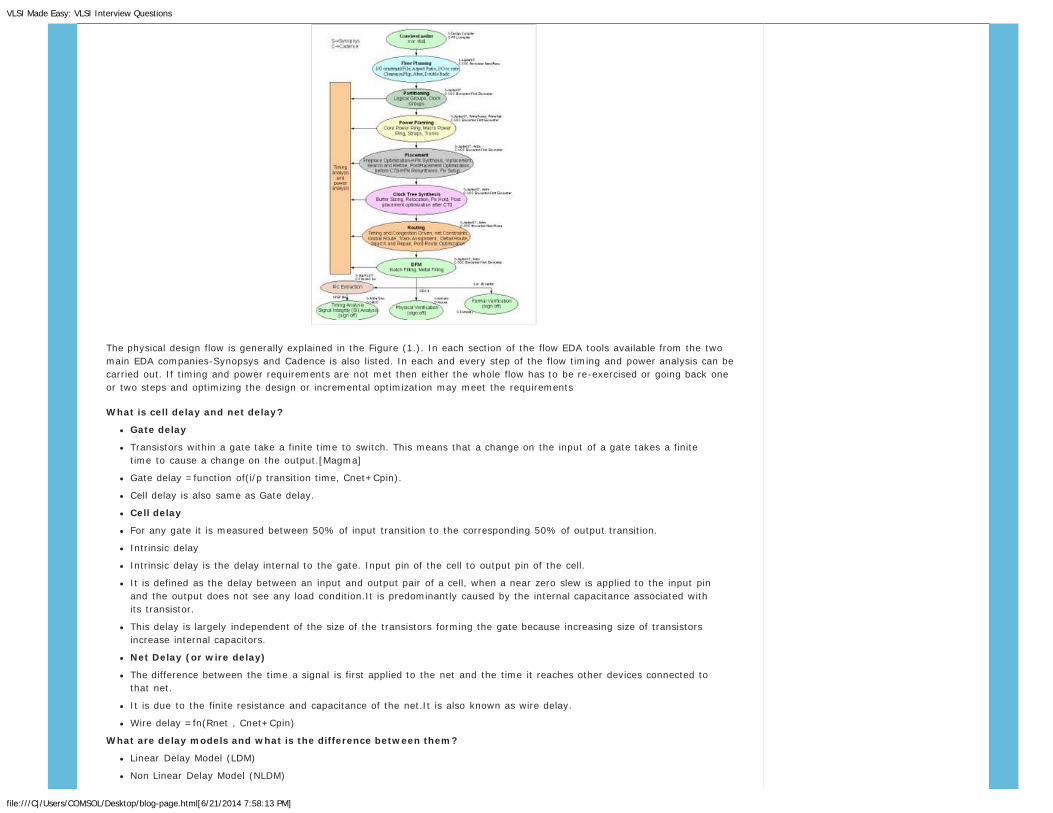
Explain the flow of physical design and inputs and outputs for each step in flow.Physical Design Flow
The physical design flow is generally explained in the Figure (1.). In each section of the flow EDA tools available from the twomain EDA companies-Synopsys and Cadence is also listed. In each and every step of the flow timing and power analysis can becarried out. If timing and power requirements are not met then either the whole flow has to be re-exercised or going back oneor two steps and optimizing the design or incremental optimization may meet the requirements
What is cell delay and net delay?
Gate delay
Transistors within a gate take a finite time to switch. This means that a change on the input of a gate takes a finitetime to cause a change on the output.[Magma]
Gate delay =function of(i/p transition time, Cnet+Cpin).
Cell delay is also same as Gate delay.
Cell delay
For any gate it is measured between 50% of input transition to the corresponding 50% of output transition.
Intrinsic delay
Intrinsic delay is the delay internal to the gate. Input pin of the cell to output pin of the cell.
It is defined as the delay between an input and output pair of a cell, when a near zero slew is applied to the input pinand the output does not see any load condition.It is predominantly caused by the internal capacitance associated withits transistor.
This delay is largely independent of the size of the transistors forming the gate because increasing size of transistorsincrease internal capacitors.
Net Delay (or wire delay)
The difference between the time a signal is first applied to the net and the time it reaches other devices connected tothat net.
It is due to the finite resistance and capacitance of the net.It is also known as wire delay.
Wire delay =fn(Rnet , Cnet+Cpin)
What are delay models and what is the difference between them?
Wire load model is NLDM which has estimated R and C of the net.
Why higher metal layers are preferred for Vdd and Vss?
Because it has less resistance and hence leads to less IR drop.
What is logic optimization and give some methods of logic optimization.
Upsizing
Downsizing
Buffer insertion
Buffer relocation
Dummy buffer placement
What is the significance of negative slack?
negative slack==> there is setup voilation==> deisgn can fail
What is signal integrity? How it affects Timing?
IR drop, Electro Migration (EM), Crosstalk, Ground bounce are signal integrity issues.
If Idrop is more==>delay increases.
crosstalk==>there can be setup as well as hold voilation.
What is IR drop? How to avoid? How it affects timing?
There is a resistance associated with each metal layer. This resistance consumes power causing voltage drop i.e.IRdrop.
If IR drop is more==>delay increases.
What is EM and it effects?
Due to high current flow in the metal atoms of the metal can displaced from its origial place. When it happens in largeramount the metal can open or bulging of metal layer can happen. This effect is known as Electro Migration.
Affects: Either short or open of the signal line or power line.
What are types of routing?
Global Routing
Track Assignment
Detail Routing
What is latency? Give the types?
Source Latency
It is known as source latency also. It is defined as "the delay from the clock origin point to the clock definition point inthe design".
Delay from clock source to beginning of clock tree (i.e. clock definition point).
The time a clock signal takes to propagate from its ideal waveform origin point to the clock definition point in thedesign.
Network latency
It is also known as Insertion delay or Network latency. It is defined as "the delay from the clock definition point to theclock pin of the register".
The time clock signal (rise or fall) takes to propagate from the clock definition point to a register clock pin.
What is track assignment?
Second stage of the routing wherein particular metal tracks (or layers) are assigned to the signal nets.
What is congestion?
If the number of routing tracks available for routing is less than the required tracks then it is known as congestion.
Whether congestion is related to placement or routing?
Distribution of clock from the clock source to the sync pin of the registers.
What are clock tree types?
H tree, Balanced tree, X tree, Clustering tree, Fish bone
What is cloning and buffering?
Cloning is a method of optimization that decreases the load of a heavily loaded cell by replicating the cell.
Buffering is a method of optimization that is used to insert beffers in high fanout nets to decrease the dealy.
ASICDifferent Types of Delays in ASIC or VLSI design
Source Delay/Latency
Network Delay/Latency
Insertion Delay
Transition Delay/Slew: Rise time, fall time
Path Delay
Net delay, wire delay, interconnect delay
Propagation Delay
Phase Delay
Cell Delay
Intrinsic Delay
Extrinsic Delay
Input Delay
Output Delay
Exit Delay
Latency (Pre/post CTS)
Uncertainty (Pre/Post CTS)
Unateness: Positive unateness, negative unateness
Jitter: PLL jitter, clock jitter
Gate delay
Transistors within a gate take a finite time to switch. This means that a change on the input of a gate takes a finitetime to cause a change on the output.[Magma]
Gate delay =function of(i/p transition time, Cnet+Cpin).
Cell delay is also same as Gate delay.
Source Delay (or Source Latency)
It is known as source latency also. It is defined as "the delay from the clock origin point to the clock definition point inthe design".
Delay from clock source to beginning of clock tree (i.e. clock definition point).
The time a clock signal takes to propagate from its ideal waveform origin point to the clock definition point in thedesign.
Network Delay(latency)
It is also known as Insertion delay or Network latency. It is defined as "the delay from the clock definition point to theclock pin of the register".
The time clock signal (rise or fall) takes to propagate from the clock definition point to a register clock pin.
The delay from the clock definition point to the clock pin of the register.
Transition delay
It is also known as "Slew". It is defined as the time taken to change the state of the signal. Time taken for thetransition from logic 0 to logic 1 and vice versa . or Time taken by the input signal to rise from 10%(20%) to the90%(80%) and vice versa.
Transition is the time it takes for the pin to change state.
Slew
Rate of change of logic.See Transition delay.
Slew rate is the speed of transition measured in volt / ns.
Rise Time
Rise time is the difference between the time when the signal crosses a low threshold to the time when the signalcrosses the high threshold. It can be absolute or percent.
Low and high thresholds are fixed voltage levels around the mid voltage level or it can be either 10% and 90%respectively or 20% and 80% respectively. The percent levels are converted to absolute voltage levels at the time ofmeasurement by calculating percentages from the difference between the starting voltage level and the final settledvoltage level.
Fall Time
Fall time is the difference between the time when the signal crosses a high threshold to the time when the signalcrosses the low threshold.
The low and high thresholds are fixed voltage levels around the mid voltage level or it can be either 10% and 90%respectively or 20% and 80% respectively. The percent levels are converted to absolute voltage levels at the time ofmeasurement by calculating percentages from the difference between the starting voltage level and the final settledvoltage level.
For an ideal square wave with 50% duty cycle, the rise time will be 0.For a symmetric triangular wave, this is reducedto just 50%.
The rise/fall definition is set on the meter to 10% and 90% based on the linear power in Watts. These points translateinto the -10 dB and -0.5 dB points in log mode (10 log 0.1) and (10 log 0.9). The rise/fall time values of 10% and90% are calculated based on an algorithm, which looks at the mean power above and below the 50% points of therise/fall timesPath delay
Path delay is also known as pin to pin delay. It is the delay from the input pin of the cell to the output pin of the cell.
Net Delay (or wire delay)
The difference between the time a signal is first applied to the net and the time it reaches other devices connected tothat net.
It is due to the finite resistance and capacitance of the net.It is also known as wire delay.
Wire delay =fn(Rnet , Cnet+Cpin)
Propagation delay
For any gate it is measured between 50% of input transition to the corresponding 50% of output transition.
This is the time required for a signal to propagate through a gate or net. For gates it is the time it takes for a event atthe gate input to affect the gate output.
For net it is the delay between the time a signal is first applied to the net and the time it reaches other devicesconnected to that net.
It is taken as the average of rise time and fall time i.e. Tpd= (Tphl+Tplh)/2.
Phase delay
Same as insertion delay
Cell delay
For any gate it is measured between 50% of input transition to the corresponding 50% of output transition.
Intrinsic delay is the delay internal to the gate. Input pin of the cell to output pin of the cell.
It is defined as the delay between an input and output pair of a cell, when a near zero slew is applied to the input pinand the output does not see any load condition.It is predominantly caused by the internal capacitance associated withits transistor.
This delay is largely independent of the size of the transistors forming the gate because increasing size of transistorsincrease internal capacitors.
Extrinsic delay
Same as wire delay, net delay, interconnect delay, flight time.
Extrinsic delay is the delay effect that associated to with interconnect. output pin of the cell to the input pin of the nextcell.
Input delay
Input delay is the time at which the data arrives at the input pin of the block from external circuit with respect toreference clock.
Output delay
Output delay is time required by the external circuit before which the data has to arrive at the output pin of the blockwith respect to reference clock.
Exit delay
It is defined as the delay in the longest path (critical path) between clock pad input and an output. It determines themaximum operating frequency of the design.
Latency (pre/post cts)
Latency is the summation of the Source latency and the Network latency. Pre CTS estimated latency will be consideredduring the synthesis and after CTS propagated latency is considered.
Uncertainty (pre/post cts)
Uncertainty is the amount of skew and the variation in the arrival clock edge. Pre CTS uncertainty is clock skew andclock Jitter. After CTS we can have some margin of skew + Jitter.
Unateness
A function is said to be unate if the rise transition on the positive unate input variable causes the ouput to rise or nochange and vice versa.
Negative unateness means cell output logic is inverted version of input logic. eg. In inverter having input A and outputY, Y is -ve unate w.r.to A. Positive unate means cell output logic is same as that of input.
These +ve ad -ve unateness are constraints defined in library file and are defined for output pin w.r.to some input pin.
A clock signal is positive unate if a rising edge at the clock source can only cause a rising edge at the register clockpin, and a falling edge at the clock source can only cause a falling edge at the register clock pin.
A clock signal is negative unate if a rising edge at the clock source can only cause a falling edge at the register clockpin, and a falling edge at the clock source can only cause a rising edge at the register clock pin. In other words, theclock signal is inverted.
A clock signal is not unate if the clock sense is ambiguous as a result of non-unate timing arcs in the clock path. Forexample, a clock that passes through an XOR gate is not unate because there are nonunate arcs in the gate. The clocksense could be either positive or negative, depending on the state of the other input to the XOR gate.
Jitter
The short-term variations of a signal with respect to its ideal position in time.
Jitter is the variation of the clock period from edge to edge. It can varry +/- jitter value.
From cycle to cycle the period and duty cycle can change slightly due to the clock generation circuitry. This can bemodeled by adding uncertainty regions around the rising and falling edges of the clock waveform.
Sources of Jitter Common sources of jitter include:
The difference in the arrival of clock signal at the clock pin of different flops.
Two types of skews are defined: Local skew and Global skew.
Local skew
The difference in the arrival of clock signal at the clock pin of related flops.
Global skew
The difference in the arrival of clock signal at the clock pin of non related flops.
Skew can be positive or negative.
When data and clock are routed in same direction then it is Positive skew.
When data and clock are routed in opposite then it is negative skew.
Recovery Time
Recovery specifies the minimum time that an asynchronous control input pin must be held stable after being de-asserted and before the next clock (active-edge) transition.
Recovery time specifies the time the inactive edge of the asynchronous signal has to arrive before the closing edge ofthe clock.
Recovery time is the minimum length of time an asynchronous control signal (eg.preset) must be stable before thenext active clock edge. The recovery slack time calculation is similar to the clock setup slack time calculation, but itapplies asynchronous control signals.
Equation 1:
Recovery Slack Time = Data Required Time – Data Arrival Time
Data Arrival Time = Launch Edge + Clock Network Delay to Source Register + Tclkq+ Register to Register Delay
Data Required Time = Latch Edge + Clock Network Delay to Destination Register =Tsetup
If the asynchronous control is not registered, equations shown in Equation 2 is used to calculate the recovery slack time.Equation 2:
Recovery Slack Time = Data Required Time – Data Arrival Time
Data Arrival Time = Launch Edge + Maximum Input Delay + Port to Register Delay
Data Required Time = Latch Edge + Clock Network Delay to Destination Register Delay+Tsetup
If the asynchronous reset signal is from a port (device I/O), you must make an Input Maximum Delay assignment tothe asynchronous reset pin to perform recovery analysis on that path.
Removal Time
Removal specifies the minimum time that an asynchronous control input pin must be held stable before being de-asserted and after the previous clock (active-edge) transition.
Removal time specifies the length of time the active phase of the asynchronous signal has to be held after the closingedge of clock.
Removal time is the minimum length of time an asynchronous control signal must be stable after the active clockedge. Calculation is similar to the clock hold slack calculation, but it applies asynchronous control signals. If theasynchronous control is registered, equations shown in Equation 3 is used to calculate the removal slack time.
If the recovery or removal minimum time requirement is violated, the output of the sequential cell becomes uncertain.The uncertainty can be caused by the value set by the resetbar signal or the value clocked into the sequential cell fromthe data input.
Removal Slack Time = Data Arrival Time – Data Required Time
Data Arrival Time = Launch Edge + Clock Network Delay to Source Register + Tclkq of Source Register + Register toRegister Delay
Data Required Time = Latch Edge + Clock Network Delay to Destination Register + Thold
If the asynchronous control is not registered, equations shown in Equation 4 is used to calculate the removal slacktime.
Equation 4
Removal Slack Time = Data Arrival Time – Data Required Time
Data Arrival Time = Launch Edge + Input Minimum Delay of Pin + Minimum Pin to Register Delay
Data Required Time = Latch Edge + Clock Network Delay to Destination Register +Thold
If the asynchronous reset signal is from a device pin, you must specify the Input Minimum Delay constraint to theasynchronous reset pin to perform a removal analysis on this path.
What is the difference between hard macro, firm macro and soft macro?
or
What are IPs?
Hard macro, firm macro and soft macro are all known as IP (Intellectual property). They are optimized for power, areaand performance. They can be purchased and used in your ASIC or FPGA design implementation flow. Soft macro isflexible for all type of ASIC implementation. Hard macro can be used in pure ASIC design flow, not in FPGA flow.Before bying any IP it is very important to evaluate its advantages and disadvantages over each other, hardwarecompatibility such as I/O standards with your design blocks, reusability for other designs.
Soft macros
Soft macros are in synthesizable RTL.
Soft macros are more flexible than firm or hard macros.
Soft macros are not specific to any manufacturing process.
Soft macros have the disadvantage of being somewhat unpredictable in terms of performance, timing, area, or power.
Soft macros carry greater IP protection risks because RTL source code is more portable and therefore, less easilyprotected than either a netlist or physical layout data.
From the physical design perspective, soft macro is any cell that has been placed and routed in a placement androuting tool such as Astro. (This is the definition given in Astro Rail user manual !)
Soft macros are editable and can contain standard cells, hard macros, or other soft macros.
Firm macros
Firm macros are in netlist format.
Firm macros are optimized for performance/area/power using a specific fabrication technology.
Firm macros are more flexible and portable than hard macros.
Firm macros are predictive of performance and area than soft macros.
Hard macro
Hard macros are generally in the form of hardware IPs (or we termed it as hardwre IPs !).
Hard macos are targeted for specific IC manufacturing technology.
Hard macros are block level designs which are silicon tested and proved.
Hard macros have been optimized for power or area or timing.
In physical design you can only access pins of hard macros unlike soft macros which allows us to manipulate indifferent way.
You have freedom to move, rotate, flip but you can't touch anything inside hard macros.
Very common example of hard macro is memory. It can be any design which carries dedicated single functionality (in
What is the difference between soft macro and hard macro?
Be aware of features and characteristics of hard macro before you use it in your design... other than power, timing andarea you also should know pin properties like sync pin, I/O standards etc
LEF, GDS2 file format allows easy usage of macros in different tools.
From the physical design (backend) perspective:
Hard macro is a block that is generated in a methodology other than place and route (i.e. using full custom designmethodology) and is brought into the physical design database (eg. Milkyway in Synopsys; Volcano in Magma) as aGDS2 file.
FPGA-Field Programmable Gate Array and CPLD-Complex Programmable Logic Device-- both are programmable logic devicesmade by the same companies with different characteristics.
"A Complex Programmable Logic Device (CPLD) is a Programmable Logic Device with complexity between that of PALs(Programmable Array Logic) and FPGAs, and architectural features of both. The building block of a CPLD is the macro cell,which contains logic implementing disjunctive normal form expressions and more specialized logic operations".
ArchitectureGranularity is the biggest difference between CPLD and FPGA.FPGA are "fine-grain" devices. That means that they contain hundreds of (up to 100000) of tiny blocks (called as LUT or
CLBs etc) of logic with flip-flops, combinational logic and memories.FPGAs offer much higher complexity, up to 150,000flip-flops and large number of gates available.
CPLDs typically have the equivalent of thousands of logic gates, allowing implementation of moderately complicated dataprocessing devices. PALs typically have a few hundred gate equivalents at most, while FPGAs typically range from tens ofthousands to several million.
CPLD are "coarse-grain" devices. They contain relatively few (a few 100's max) large blocks of logic with flip-flops andcombinational logic. CPLDs based on AND-OR structure.
CPLD's have a register with associated logic (AND/OR matrix). CPLD's are mostly implemented in control applications andFPGA's in datapath applications. Because of this course grained architecture, the timing is very fixed in CPLDs.
FPGA are RAM based. They need to be "downloaded" (configured) at each power-up. CPLD are EEPROM based.They are active at power-up i.e. as long as they've been programmed at least once.
FPGA needs boot ROM but CPLD does not. In some systems you might not have enough time to boot up FPGA then you needCPLD+FPGA.
Generally, the CPLD devices are not volatile, because they contain flash or erasable ROM memory in all the cases. The FPGAare volatile in many cases and hence they need a configuration memory for working. There are some FPGAs now whichare nonvolatile. This distinction is rapidly becoming less relevant, as several of the latest FPGA products also offer modelswith embedded configuration memory.
The characteristic of non-volatility makes the CPLD the device of choice in modern digital designs to perform 'bootloader' functions before handing over control to other devices not having this capability. A good example is where aCPLD is used to load configuration data for an FPGA from non-volatile memory.
Because of coarse-grain architecture, one block of logic can hold a big equation and hence CPLD have a faster input-to-output timings than FPGA.
Features
FPGA have special routing resources to implement binary counters,arithmetic functions like adders, comparators andRAM. CPLD don't have special features like this.
FPGA can contain very large digital designs, while CPLD can contain small designs only.The limited complexity (<500>
Speed: CPLDs offer a single-chip solution with fast pin-to-pin delays, even for wide input functions. Use CPLDs forsmall designs, where "instant-on", fast and wide decoding, ultra-low idle power consumption, and design security areimportant (e.g., in battery-operated equipment).
Security: In CPLD once programmed, the design can be locked and thus made secure. Since the configurationbitstream must be reloaded every time power is re-applied, design security in FPGA is an issue.
Power: The high static (idle) power consumption prohibits use of CPLD in battery-operated equipment. FPGA idlepower consumption is reasonably low, although it is sharply increasing in the newest families.
Design flexibility: FPGAs offer more logic flexibility and more sophisticated system features than CPLDs: clockmanagement, on-chip RAM, DSP functions, (multipliers), and even on-chip microprocessors and Multi-Gigabit
Transceivers.These benefits and opportunities of dynamic reconfiguration, even in the end-user system, are animportant advantage.
Use FPGAs for larger and more complex designs.
FPGA is suited for timing circuit becauce they have more registers , but CPLD is suited for control circuit because theyhave more combinational circuit. At the same time, If you synthesis the same code for FPGA for many times, you willfind out that each timing report is different. But it is different in CPLD synthesis, you can get the same result.
As CPLDs and FPGAs become more advanced the differences between the two device types will continue to blur. While this trendmay appear to make the two types more difficult to keep apart, the architectural advantage of CPLDs combining low cost, non-volatile configuration, and macro cells with predictable timing characteristics will likely be sufficient to maintain a productdifferentiation for the foreseeable future.
This question is very popular in VLSI fresher interviews. It looks simple but a deeper insight into the subject reveals the factthat there are lot of thinks to be understood !! So here is the answer.
FPGA vs. ASIC
Difference between ASICs and FPGAs mainly depends on costs, tool availability, performance and design flexibility.They have their own pros and cons but it is designers responsibility to find the advantages of the each and use eitherFPGA or ASIC for the product. However, recent developments in the FPGA domain are narrowing down the benefits ofthe ASICs.
FPGA
Field Programable Gate Arrays
FPGA Design Advantages
Faster time-to-market: No layout, masks or other manufacturing steps are needed for FPGA design. ReadymadeFPGA is available and burn your HDL code to FPGA ! Done !!
No NRE (Non Recurring Expenses): This cost is typically associated with an ASIC design. For FPGA this is not there.FPGA tools are cheap. (sometimes its free ! You need to buy FPGA.... thats all !). ASIC youpay huge NRE and tools areexpensive. I would say "very expensive"...Its in crores....!!
Simpler design cycle: This is due to software that handles much of the routing, placement, and timing. Manualintervention is less.The FPGA design flow eliminates the complex and time-consuming floorplanning, place and route,timing analysis.
More predictable project cycle: The FPGA design flow eliminates potential re-spins, wafer capacities, etc of theproject since the design logic is already synthesized and verified in FPGA device.
Field Reprogramability: A new bitstream ( i.e. your program) can be uploaded remotely, instantly. FPGA can bereprogrammed in a snap while an ASIC can take $50,000 and more than 4-6 weeks to make the same changes. FPGAcosts start from a couple of dollars to several hundreds or more depending on the hardware features.
Reusability: Reusability of FPGA is the main advantage. Prototype of the design can be implemented on FPGA whichcould be verified for almost accurate results so that it can be implemented on an ASIC. Ifdesign has faults change theHDL code, generate bit stream, program to FPGA and test again.Modern FPGAs are reconfigurable both partially anddynamically.
FPGAs are good for prototyping and limited production.If you are going to make 100-200 boards it isn't worth to make anASIC.
Generally FPGAs are used for lower speed, lower complexity and lower volume designs.But today's FPGAs even run at 500MHz with superior performance. With unprecedented logic density increases and a host of other features, such asembedded processors, DSP blocks, clocking, and high-speed serial at ever lower price, FPGAs are suitable for almost anytype of design.
Unlike ASICs, FPGA's have special hardwares such as Block-RAM, DCM modules, MACs, memories and highspeed I/O,embedded CPU etc inbuilt, which can be used to get better performace. Modern FPGAs are packed with features.Advanced FPGAs usually come with phase-locked loops, low-voltage differential signal, clock data recovery, moreinternal routing, high speed, hardware multipliers for DSPs, memory,programmable I/O, IP cores and microprocessorcores. Remember Power PC (hardcore) and Microblaze (softcore) in Xilinx and ARM (hardcore) and Nios(softcore) inAltera. There are FPGAs available now with built in ADC ! Using all these features designers can build a system on achip. Now, dou yo really need an ASIC ?
In FPGA you need not do floor-planning, tool can do it efficiently. In ASIC you have do it.
FPGA Design Disadvantages
Powe consumption in FPGA is more. You don't have any control over the power optimization. This is where ASIC winsthe race !
You have to use the resources available in the FPGA. Thus FPGA limits the design size.
Good for low quantity production. As quantity increases cost per product increases compared to the ASICimplementation.
ASIC
Application Specific Intergrated Circiut
ASIC Design Advantages
Cost....cost....cost....Lower unit costs: For very high volume designs costs comes out to be very less. Largervolumes of ASIC design proves to be cheaper than implementing design using FPGA.
Speed...speed...speed....ASICs are faster than FPGA: ASIC gives design flexibility. This gives enoromousopportunity for speed optimizations.
Low power....Low power....Low power: ASIC can be optimized for required low power. There are several low powertechniques such as power gating, clock gating, multi vt cell libraries, pipelining etc are available to achieve the powertarget. This is where FPGA fails badly !!! Can you think of a cell phone which has to be charged for everycall.....never.....low power ASICs helps battery live longer life !!
In ASIC you can implement analog circuit, mixed signal designs. This is generally not possible in FPGA.
In ASIC DFT (Design For Test) is inserted. In FPGA DFT is not carried out (rather for FPGA no need of DFT !) .
ASIC Design Diadvantages
Time-to-market: Some large ASICs can take a year or more to design. A good way to shorten development time isto make prototypes using FPGAs and then switch to an ASIC.
Design Issues: In ASIC you should take care of DFM issues, Signal Integrity isuues and many more. In FPGA youdon't have all these because ASIC designer takes care of all these. ( Don't forget FPGA isan IC and designed by ASICdesign enginner !!)
Expensive Tools: ASIC design tools are very much expensive. You spend a huge amount of NRE.
Structured ASICS
Structured ASICs have the bottom metal layers fixed and only the top layers can be designed by the customer.
Structured ASICs are custom devices that approach the performance of today's Standard Cell ASIC while dramaticallysimplifying the design complexity.
Structured ASICs offer designers a set of devices with specific, customizable metal layers along with predefined metallayers, which can contain the underlying pattern of logic cells, memory, and I/O.
What exact process are you using?How many layers can be used for this design?Are the Cross talk Noise constraints, Xtalk Analysis configuration, Cell EM & Wire EM available?
Design Characteristics
What is the design application?Number of cells (placeable objects)?Is the design Verilog or VHDL?Is the netlist flat or hierarchical?Is there RTL available?Is there any datapath logic using special datapath tools?Is the DFT to be considered?Can scan chains be reordered?Is memory BIST, boundary scan used on this design?Are static timing analysis constraints available in SDC format?
Clock Characteristics
How many clock domains are in the design?What are the clock frequencies?Is there a target clock skew, latency or other clock requirements?Does the design have a PLL?If so, is it used to remove clock latency?Is there any I/O cell in the feedback path?Is the PLL used for frequency multipliers?Are there derived clocks or complex clock generation circuitry?Are there any gated clocks?If yes, do they use simple gating elements?Is the gate clock used for timing or power?
For gated clocks, can the gating elements be sized for timing?Are you muxing in a test clock or using a JTAG clock?Available cells for clock tree?Are there any special clock repeaters in the library?Are there any EM, slew or capacitance limits on these repeaters?How many drive strengths are available in the standard buffers and inverters?Do any of the buffers have balanced rise and fall delays?Any there special requirements for clock distribution?Will the clock tree be shielded? If so, what are the shielding requirements?
Floorplan and Package Characteristics
Target die area?Does the area estimate include power/signal routing?What gates/mm2 has been assumed?Number of routing layers?Any special power routing requirements?Number of digital I/O pins/pads?Number of analog signal pins/pads?Number of power/ground pins/pads?Total number of pins/pads and Location?Will this chip use a wire bond package?Will this chip use a flip-chip package?If Yes, is it I/O bump pitch? Rows of bumps? Bump allocation?Bump pad layout guide?Have you already done floorplanning for this design?If yes, is conformance to the existing floorplan required?What is the target die size?What is the expected utilization?Please draw the overall floorplan ?Is there an existing floorplan available in DEF?What are the number and type of macros (memory, PLL, etc.)?Are there any analog blocks in the design?What kind of packaging is used? Flipchip?Are the I/Os periphery I/O or area I/O?How many I/Os?Is the design pad limited?Power planning and Power analysis for this design?Are layout databases available for hard macros ?Timing analysis and correlatio?Physical verification ?
Data Input
Library information for new library.lib for timing informationGDSII or LEF for library cells including any RAMsRTL in Verilog/VHDL formatNumber of logical blocks in the RTLConstraints for the block in SDCFloorplan information in DEFI/O pin locationMacro locations
General ASIC questions are posted here. More questions related to different catagories of ASICs can be found at respectivesections.
What are the differences between PALs, PLAs, FPGAs, ASICs and PLDs?In system with insufficient hold time, will slowing down the clock help?In system with insufficient setup time, will slowing down the clock help?Why would a testbench not have pins (port) on it?When declaring a flip flop, why would not you declare its output value in the port statement?Give 2 advantages of using a script to build a chip?A “tri state “ bus is directly connected to a set of CMOS input buffers. No other wires or components are attached tothe bus wires. Upon observation we can find that under certain conditions, this circuit is consuming considerable power.Why it is so? Is circuit correct? If not, how to correct?Is Verilog (or that matter any HDL) is a concurrent or sequential language?What is the function of sensitivity list?A mealy –type state machine is coded using D-type rising edge flip flops. The reset and clock signals are in thesensitivity list but with one of the next state logic input signals have been left out of the sensitivity list. Explain whathappens when the state machine is simulated? Will the state machine be synthesized correctly?A moore –type state machine is coded using D-type rising edge flip flops. The reset and clock signals are in thesensitivity list but with one of the next state logic input signals have been left out of the sensitivity list. Explain whathappens when the state machine is simulated? Will the state machine be synthesized correctly?What type of delay is most like a infinite bandwidth transmission line?Define metastability.When does metastability occur?Give one example of a situation where metastability could occur.Give two ways metastability could manifest itself in a state machine.What is MTBF?Does MTBF give the time until the next failure occurs?Give 3 ways in which to reduce the chance of metastable failure.Give 2 advantages of using a synchronous reset methodology.Give 2 disadvantages of using a synchronous reset methodology.Give 2 advantages of using an asynchronous reset methodology.Give 2 disadvantages of using an asynchronous reset methodology.What are the two most fundamental inputs (files) to the synthesis tool?What are two important steps in synthesis? What happens in those steps?What are the two major output (files) from the synthesis process?Name the fundamental 3 operating consitions that determine (globally) the delay characteristics of CMOS gates. Foreach how they affect gate delay?For a single gate, with global gating conditions held constant , what 3 delay coefficients effect total gate delay? Whichis the most sensitive to circuit topology?
FPGA.
FPGA-Field Programmable Gate Array and CPLD-Complex Programmable Logic Device-- both are programmable logic devicesmade by the same companies with different characteristics.
"A Complex Programmable Logic Device (CPLD) is a Programmable Logic Device with complexity between that of PALs(Programmable Array Logic) and FPGAs, and architectural features of both. The building block of a CPLD is the macrocell, which contains logic implementing disjunctive normal form expressions and more specialized logic operations".
This is what Wiki defines.....!!
Architecture
Granularity is the biggest difference between CPLD and FPGA.
FPGA are "fine-grain" devices. That means that they contain hundreds of (up to 100000) of tiny blocks (called asLUT or CLBs etc) of logic with flip-flops, combinational logic and memories.FPGAs offer much higher complexity, up to150,000 flip-flops and large number of gates available.
CPLDs typically have the equivalent of thousands of logic gates, allowing implementation of moderately complicateddata processing devices. PALs typically have a few hundred gate equivalents at most, while FPGAs typically range fromtens of thousands to several million.
CPLD are "coarse-grain" devices. They contain relatively few (a few 100's max) large blocks of logic with flip-flops andcombinational logic. CPLDs based on AND-OR structure.
CPLD's have a register with associated logic (AND/OR matrix). CPLD's are mostly implemented in control applications andFPGA's in datapath applications. Because of this course grained architecture, the timing is very fixed in CPLDs.
FPGA are RAM based. They need to be "downloaded" (configured) at each power-up. CPLD are EEPROM based. They areactive at power-up i.e. as long as they've been programmed at least once.
FPGA needs boot ROM but CPLD does not. In some systems you might not have enough time to boot up FPGA then you needCPLD+FPGA.
Generally, the CPLD devices are not volatile, because they contain flash or erasable ROM memory in all the cases. TheFPGA are volatile in many cases and hence they need a configuration memory for working. There are some FPGAs nowwhich are nonvolatile. This distinction is rapidly becoming less relevant, as several of the latest FPGA products alsooffer models with embedded configuration memory.
The characteristic of non-volatility makes the CPLD the device of choice in modern digital designs to perform 'bootloader' functions before handing over control to other devices not having this capability. A good example is where aCPLD is used to load configuration data for an FPGA from non-volatile memory.
Because of coarse-grain architecture, one block of logic can hold a big equation and hence CPLD have a faster input-to-output timings than FPGA.
Features
FPGA have special routing resources to implement binary counters,arithmetic functions like adders, comparators andRAM. CPLD don't have special features like this.
FPGA can contain very large digital designs, while CPLD can contain small designs only.The limited complexity (<500>
Speed: CPLDs offer a single-chip solution with fast pin-to-pin delays, even for wide input functions. Use CPLDs forsmall designs, where "instant-on", fast and wide decoding, ultra-low idle power consumption, and design security areimportant (e.g., in battery-operated equipment).
Security: In CPLD once programmed, the design can be locked and thus made secure. Since the configurationbitstream must be reloaded every time power is re-applied, design security in FPGA is an issue.
Power: The high static (idle) power consumption prohibits use of CPLD in battery-operated equipment. FPGA idlepower consumption is reasonably low, although it is sharply increasing in the newest families.
Design flexibility: FPGAs offer more logic flexibility and more sophisticated system features than CPLDs: clock management,on-chip RAM, DSP functions, (multipliers), and even on-chip microprocessors and Multi-Gigabit Transceivers.Thesebenefits and opportunities of dynamic reconfiguration, even in the end-user system, are an important advantage.
Use FPGAs for larger and more complex designs.
FPGA is suited for timing circuit becauce they have more registers , but CPLD is suited for control circuit because theyhave more combinational circuit. At the same time, If you synthesis the same code for FPGA for many times, you willfind out that each timing report is different. But it is different in CPLD synthesis, you can get the same result.
As CPLDs and FPGAs become more advanced the differences between the two device types will continue to blur. While this trendmay appear to make the two types more difficult to keep apart, the architectural advantage of CPLDs combining low cost, non-volatile configuration, and macro cells with predictable timing characteristics will likely be sufficient to maintain a productdifferentiation for the foreseeable future.
This question is very popular in VLSI fresher interviews. It looks simple but a deeper insight into the subject revealsthe fact that there are lot of thinks to be understood !! So here is the answer.
FPGA vs. ASIC
Difference between ASICs and FPGAs mainly depends on costs, tool availability, performance and design flexibility.They have their own pros and cons but it is designers responsibility to find the advantages of the each and use eitherFPGA or ASIC for the product. However, recent developments in the FPGA domain are narrowing down the benefits ofthe ASICs.
Faster time-to-market: No layout, masks or other manufacturing steps are needed for FPGA design. ReadymadeFPGA is available and burn your HDL code to FPGA ! Done !!
No NRE (Non Recurring Expenses): This cost is typically associated with an ASIC design. For FPGA this is not there.FPGA tools are cheap. (sometimes its free ! You need to buy FPGA.... thats all !). ASIC youpay huge NRE and tools areexpensive. I would say "very expensive"...Its in crores....!!
Simpler design cycle: This is due to software that handles much of the routing, placement, and timing. Manualintervention is less.The FPGA design flow eliminates the complex and time-consuming floorplanning, place and route,timing analysis.
More predictable project cycle: The FPGA design flow eliminates potential re-spins, wafer capacities, etc of theproject since the design logic is already synthesized and verified in FPGA device.
Field Reprogramability: A new bitstream ( i.e. your program) can be uploaded remotely, instantly. FPGA can bereprogrammed in a snap while an ASIC can take $50,000 and more than 4-6 weeks to make the same changes. FPGAcosts start from a couple of dollars to several hundreds or more depending on the hardware features.
Reusability: Reusability of FPGA is the main advantage. Prototype of the design can be implemented on FPGA which couldbe verified for almost accurate results so that it can be implemented on an ASIC. Ifdesign has faults change the HDLcode, generate bit stream, program to FPGA and test again.Modern FPGAs are reconfigurable both partially anddynamically.
FPGAs are good for prototyping and limited production.If you are going to make 100-200 boards it isn't worth to makean ASIC.
Generally FPGAs are used for lower speed, lower complexity and lower volume designs.But today's FPGAs even run at500 MHz with superior performance. With unprecedented logic density increases and a host of other features, such asembedded processors, DSP blocks, clocking, and high-speed serial at ever lower price, FPGAs are suitable for almostany type of design.
Unlike ASICs, FPGA's have special hardwares such as Block-RAM, DCM modules, MACs, memories and highspeed I/O,embedded CPU etc inbuilt, which can be used to get better performace. Modern FPGAs are packed with features.Advanced FPGAs usually come with phase-locked loops, low-voltage differential signal, clock data recovery, moreinternal routing, high speed, hardware multipliers for DSPs, memory,programmable I/O, IP cores and microprocessorcores. Remember Power PC (hardcore) and Microblaze (softcore) in Xilinx and ARM (hardcore) and Nios(softcore) inAltera. There are FPGAs available now with built in ADC ! Using all these features designers can build a system on achip. Now, dou yo really need an ASIC ?
FPGA sythesis is much more easier than ASIC.
In FPGA you need not do floor-planning, tool can do it efficiently. In ASIC you have do it.
FPGA Design Disadvantages
Powe consumption in FPGA is more. You don't have any control over the power optimization. This is where ASIC winsthe race !
You have to use the resources available in the FPGA. Thus FPGA limits the design size.
Good for low quantity production. As quantity increases cost per product increases compared to the ASICimplementation.
ASICApplication Specific Intergrated Circiut
ASIC Design AdvantagesCost....cost....cost....Lower unit costs: For very high volume designs costs comes out to be very less. Larger volumes of
ASIC design proves to be cheaper than implementing design using FPGA.
Speed...speed...speed....ASICs are faster than FPGA: ASIC gives design flexibility. This gives enoromousopportunity for speed optimizations.
Low power....Low power....Low power: ASIC can be optimized for required low power. There are several low powertechniques such as power gating, clock gating, multi vt cell libraries, pipelining etc are available to achieve the powertarget. This is where FPGA fails badly !!! Can you think of a cell phone which has to be charged for everycall.....never.....low power ASICs helps battery live longer life !!
In ASIC you can implement analog circuit, mixed signal designs. This is generally not possible in FPGA.
In ASIC DFT (Design For Test) is inserted. In FPGA DFT is not carried out (rather for FPGA no need of DFT !) .
ASIC Design Diadvantages
Time-to-market: Some large ASICs can take a year or more to design. A good way to shorten development time isto make prototypes using FPGAs and then switch to an ASIC.
Design Issues: In ASIC you should take care of DFM issues, Signal Integrity isuues and many more. In FPGA youdon't have all these because ASIC designer takes care of all these. ( Don't forget FPGA isan IC and designed by ASICdesign enginner !!)
Expensive Tools: ASIC design tools are very much expensive. You spend a huge amount of NRE.
Structured ASICS
Structured ASICs have the bottom metal layers fixed and only the top layers can be designed by the customer.
Structured ASICs are custom devices that approach the performance of today's Standard Cell ASIC while dramaticallysimplifying the design complexity.
Structured ASICs offer designers a set of devices with specific, customizable metal layers along with predefined metallayers, which can contain the underlying pattern of logic cells, memory, and I/O.
· What is minimum and maximum frequency of DCM in spartan-3 series FPGA? · List some of constraints you used and their purpose during your design?· What is the size of bitmap with changing gate count?· What are different types of FPGA programming modes? How to change from one to another?· List out some important features of FPGA.· List out some of synthesizable and non synthesizable constructs?· Draw general structure of FPGA?· What is the difference between FPGA and CPLD?· What is DCM? Why they are used?· Draw FPGA design flow. Explain each step. What is input and output from each step?· What is slice, CLB, LUT?· Is it possible to configure CLB as RAM?· What is purpose of a constraint file? What is its extension?· How you will choose an FPGA?· How clock is routed through out FPGA?· What are difference between PLL and DLL ?· What is soft processor?· What is hard processor?