BMS INSTITUTE OF TECHNOLOGY AND MANAGEMENT YELAHANKA – BANGALORE - 64 DEPARTMENT OF COMPUTER SCIENCE & ENGINEERING III INTERNAL ASSESSMENT SCHEME & SOLUTIONS, MAY – 2017 Subject: Microprocessors & Microcontrollers Subject Code: 15CS44 Branch & Semester : CSE - 4 A & B Max. Marks : 30 Marks Date: 23/05/2017 Time: 2 PM - 3:30 PM Faculty: Mr. Shankar R Answer FIVE full questions, selecting ONE full question from each Part. (Part D & Part E are compulsory) Q. No Question CO, PO, K level Marks PART-A 1. Describe the different features of ARM instruction set that make it suitable for embedded applications. Explanation 6 marks The ARM instruction set differs from the pure RISC definition in several ways that make the ARM instruction set suitable for embedded applications: ■ Variable cycle execution for certain instructions—Not every ARM instruction executes in a single cycle. For example, load-store-multiple instructions vary in the number of execution cycles depending upon the number of registers being transferred. The transfer can occur on sequential memory addresses, which increases performance since sequential memory accesses are often faster than random accesses. Code density is also improved since multiple register transfers are common operations at the start and end of functions. ■ Inline barrel shifter leading to more complex instructions—The inline barrel shifter is a hardware component that pre-processes one of the input registers before it is used by an instruction. This expands the capability of many instructions to improve core performance and code density. We explain this feature in more detail in Chapters 2, 3, and 4. ■ Thumb 16-bit instruction set—ARM enhanced the processor core by adding a second 16-bit instruction set called Thumb that permits the ARM core to execute either 16- or 32-bit instructions. The 16-bit instructions improve code density by about 30% over 32-bit fixed-length instructions. ■ Conditional execution—An instruction is only executed when a specific condition has been satisfied. This feature improves performance and code density by reducing branch instructions. ■ Enhanced instructions—The enhanced digital signal processor (DSP) instructions were added to the standard ARM instruction set to support fast 16×16-bit multiplier operations and saturation. These instructions allow a faster-performing ARM processor in some cases to replace the traditional combinations of a processor plus a DSP. CO3 (PO1) K2 06 2. Explain ARM core dataflow model with a neat diagram. Diagram 2 marks Explanation 4 marks Data enters the processor core through the Data bus. The data may be an instruction to execute or a data item. Figure shows a Von Neumann implementation of the ARM— data items and instructions share the same bus. In contrast, Harvard implementations of the ARM use two different buses. The instruction decoder translates instructions CO3 (PO1) K2 06
Transcript
BMS INSTITUTE OF TECHNOLOGY AND MANAGEMENT YELAHANKA – BANGALORE - 64
DEPARTMENT OF COMPUTER SCIENCE & ENGINEERING
III INTERNAL ASSESSMENT SCHEME & SOLUTIONS, MAY – 2017 Subject: Microprocessors &
Microcontrollers Subject Code: 15CS44 Branch & Semester : CSE - 4 A & B
Max. Marks : 30 Marks Date: 23/05/2017
Time: 2 PM - 3:30 PM Faculty: Mr. Shankar R
Answer FIVE full questions, selecting ONE full question from each Part. (Part D & Part E are compulsory)
Q. No Question CO, PO, K level
Marks
PART-A
1.
Describe the different features of ARM instruction set that make it
suitable for embedded applications.
Explanation 6 marks
The ARM instruction set differs from the pure RISC definition in several ways that
make the ARM instruction set suitable for embedded applications:
■ Variable cycle execution for certain instructions—Not every ARM instruction
executes in a single cycle. For example, load-store-multiple instructions vary in the
number of execution cycles depending upon the number of registers being transferred.
The transfer can occur on sequential memory addresses, which increases performance
since sequential memory accesses are often faster than random accesses. Code density
is also improved since multiple register transfers are common operations at the start and end of functions.
■ Inline barrel shifter leading to more complex instructions—The inline barrel
shifter is a hardware component that pre-processes one of the input registers before it
is used by an instruction. This expands the capability of many instructions to improve
core performance and code density. We explain this feature in more detail in Chapters
2, 3, and 4.
■ Thumb 16-bit instruction set—ARM enhanced the processor core by adding a
second 16-bit instruction set called Thumb that permits the ARM core to execute either
16- or 32-bit instructions. The 16-bit instructions improve code density by about 30%
over 32-bit fixed-length instructions.
■ Conditional execution—An instruction is only executed when a specific condition has been satisfied. This feature improves performance and code density by reducing
branch instructions.
■ Enhanced instructions—The enhanced digital signal processor (DSP) instructions
were added to the standard ARM instruction set to support fast 16×16-bit multiplier
operations and saturation. These instructions allow a faster-performing ARM
processor in some cases to replace the traditional combinations of a processor plus a
DSP.
CO3
(PO1)
K2 06
2.
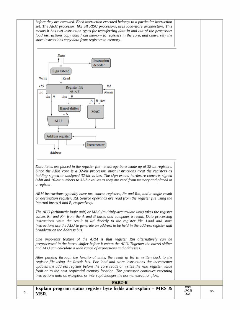
Explain ARM core dataflow model with a neat diagram.
Diagram 2 marks
Explanation 4 marks
Data enters the processor core through the Data bus. The data may be an instruction
to execute or a data item. Figure shows a Von Neumann implementation of the ARM— data items and instructions share the same bus. In contrast, Harvard implementations
of the ARM use two different buses. The instruction decoder translates instructions
CO3 (PO1) K2
06
before they are executed. Each instruction executed belongs to a particular instruction
set. The ARM processor, like all RISC processors, uses load-store architecture. This
means it has two instruction types for transferring data in and out of the processor:
load instructions copy data from memory to registers in the core, and conversely the
store instructions copy data from registers to memory.
Data items are placed in the register file—a storage bank made up of 32-bit registers.
Since the ARM core is a 32-bit processor, most instructions treat the registers as
holding signed or unsigned 32-bit values. The sign extend hardware converts signed 8-bit and 16-bit numbers to 32-bit values as they are read from memory and placed in
a register.
ARM instructions typically have two source registers, Rn and Rm, and a single result
or destination register, Rd. Source operands are read from the register file using the
internal buses A and B, respectively.
The ALU (arithmetic logic unit) or MAC (multiply-accumulate unit) takes the register
values Rn and Rm from the A and B buses and computes a result. Data processing
instructions write the result in Rd directly to the register file. Load and store
instructions use the ALU to generate an address to be held in the address register and
broadcast on the Address bus.
One important feature of the ARM is that register Rm alternatively can be
preprocessed in the barrel shifter before it enters the ALU. Together the barrel shifter and ALU can calculate a wide range of expressions and addresses.
After passing through the functional units, the result in Rd is written back to the
register file using the Result bus. For load and store instructions the incrementer
updates the address register before the core reads or writes the next register value
from or to the next sequential memory location. The processor continues executing
instructions until an exception or interrupt changes the normal execution flow.
PART-B
3. Explain program status register byte fields and explain – MRS &
MSR.
CO3
(PO1) K2
06
The ARM instruction set provides two instructions to directly control a program status register (psr). The MRS instruction transfers the contents of either the cpsr or spsr into a register; in the reverse direction, the MSR instruction transfers the contents of a register into the cpsr or spsr. Together these instructions are used to read and write the cpsr and spsr.
In the syntax you can see a label called fields. This can be any combination of control (c), extension (x), status (s), and flags (f ). These fields relate to particular byte regions in a psr, as shown in Figure. Syntax: MRS{<cond>} Rd,<cpsr|spsr> MSR{<cond>} <cpsr|spsr>_<fields>,Rm MSR{<cond>} <cpsr|spsr>_<fields>,#immediate
The c field controls the interrupt masks, Thumb state, and processor mode. The following Example shows how to enable IRQ interrupts by clearing the I mask. This operation involves using both the MRS and MSR instructions to read from and then write to the cpsr. The MSR first copies the cpsr into register r1. The BIC instruction clears bit 7 of r1. Register r1 is then copied back into the cpsr, which enables IRQ interrupts. You can see from this example that this code preserves all the other settings in the cpsr and only modifies the I bit in the control field. PRE cpsr = nzcvqIFt_SVC MRS r1, cpsr BIC r1, r1, #0x80 ; 0b01000000 MSR cpsr_c, r1 POST cpsr = nzcvqiFt_SVC
This example is in SVC mode. In user mode you can read all cpsr bits, but you can only update the condition flag field f.
4.
With example, illustrate how following instructions work?
LDRSH STRB LDMDA STMIA
Each instruction 1.5 marks * 4 – 6 marks
1. LDRSH The LDRSH instruction loads a halfword from addr_mode into dest . The halfword is sign-extended into a 32-bit word enabling 16-bit memory data to be manipulated. It also enables PC-relative addressing if used as a base register. The condition needs to be
CO4 (PO1) K3
06
a valid value; else the instruction is rendered an NOP. Syntax
LDR[condition]SH dest, addr_mode LDRSH R2, [R0]
2. STRB save byte from a register - Rd -> mem8[address]
What are banked registers? Show how the banked registers are
utilized when the user mode changes to IRQ mode?
The above figure shows all 37 registers in the register file. Of those, 20 registers are hidden from a program at different times. These registers are called banked registers and are identified by the shading in the diagram. They are available only when the processor is in a particular mode; for example, abort mode has banked registers r13_abt, r14_abt and spsr_abt. Banked registers of a particular mode are denoted by an underline character post-fixed to the mode mnemonic or _mode.
For example, when the processor is in the interrupt request mode, the instructions you execute still access registers named r13 and r14. However, these registers are the banked registers r13_irq and r14_irq. The user mode registers r13_usr and r14_usr are not affected by the instruction referencing these registers. A program still has normal access to the other registers r0 to r12.
CO3
(PO2) K3
06
Figure illustrates what happens when an interrupt forces a mode change. The figure shows the core changing from user mode to interrupt request mode, which happens when an interrupt request occurs due to an external device raising an interrupt to the processor core. This change causes user registers r13 and r14 to be banked. The user registers are replaced with registers r13_irq and r14_irq, respectively. Note r14_irq contains the return address and r13_irq contains the stack pointer for interrupt request mode.
Figure also shows a new register appearing in interrupt request mode: the saved program status register (spsr), which stores the previous mode’s cpsr. You can see in the diagram the cpsr being copied into spsr_irq. To return back to user mode, a special return instruction is used that instructs the core to restore the original cpsr from the spsr_irq and bank in the user registers r13 and r14. Note that the spsr can only be modified and read in a privileged mode. There is no spsr available in user mode.
6.
Explain in detail Arithmetic instructions. How Barrel shifter is used
with Arithmetic instructions?
Explanation of both – 3 marks * 2 – 6 marks
Arithmetic Instructions
The arithmetic instructions implement addition and subtraction of 32-bit signed and
unsigned values.
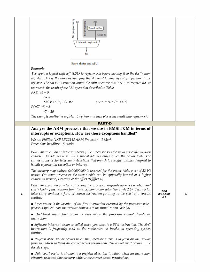
Barrel Shifter
In MOV instruction, the second operand N can be more than just a register or
immediate value; it can also be a register Rm that has been preprocessed by the barrel
shifter prior to being used by a data processing instruction. Data processing
instructions are processed within the arithmetic logic unit (ALU). A unique and
powerful feature of the ARM processor is the ability to shift the 32-bit binary pattern
in one of the source registers left or right by a specific number of positions before it
enters the ALU. This shift increases the power and flexibility of many data processing
operations.
There are data processing instructions that do not use the barrel shift, for example, the
MUL (multiply), CLZ (count leading zeros), and QADD (signed saturated 32-bit
add) instructions.
Pre-processing or shift occurs within the cycle time of the instruction. This is
particularly useful for loading constants into a register and achieving fast multiplies
or division by a power of 2.
CO3 (PO2)
K2 06
Example
We apply a logical shift left (LSL) to register Rm before moving it to the destination
register. This is the same as applying the standard C language shift operator to the
register. The MOV instruction copies the shift operator result N into register Rd. N
represents the result of the LSL operation described in Table.
PRE r5 = 5
r7 = 8
MOV r7, r5, LSL #2 ; r7 = r5*4 = (r5 << 2)
POST r5 = 5
r7 = 20
The example multiplies register r5 by four and then places the result into register r7.
PART-D
7.
Analyze the ARM processor that we use in BMSIT&M in terms of
interrupts or exceptions. How are those exceptions handled?
We use Phillips NXP LPC2148 ARM Processor – 1 Mark Exceptions handling – 5 marks When an exception or interrupt occurs, the processor sets the pc to a specific memory address. The address is within a special address range called the vector table. The entries in the vector table are instructions that branch to specific routines designed to handle a particular exception or interrupt.
The memory map address 0x00000000 is reserved for the vector table, a set of 32-bit words. On some processors the vector table can be optionally located at a higher address in memory (starting at the offset 0xffff0000).
When an exception or interrupt occurs, the processor suspends normal execution and starts loading instructions from the exception vector table (see Table 2.6). Each vector table entry contains a form of branch instruction pointing to the start of a specific routine:
■ Reset vector is the location of the first instruction executed by the processor when power is applied. This instruction branches to the initialization code.
■ Undefined instruction vector is used when the processor cannot decode an instruction.
■ Software interrupt vector is called when you execute a SWI instruction. The SWI instruction is frequently used as the mechanism to invoke an operating system routine.
■ Prefetch abort vector occurs when the processor attempts to fetch an instruction from an address without the correct access permissions. The actual abort occurs in the decode stage.
■ Data abort vector is similar to a prefetch abort but is raised when an instruction attempts to access data memory without the correct access permissions.
CO3
(PO1,PO2) K4
06
■ Interrupt request vector is used by external hardware to interrupt the normal execution flow of the processor. It can only be raised if IRQs are not masked in the cpsr.
■ Fast interrupt request vector is similar to the interrupt request but is reserved for hardware requiring faster response times. It can only be raised if FIQs are not masked in the cpsr.
PART - E
8.
Assess the result of this instruction (post computation).
PRE r1 = 0b1111
r2 = 0b0101
BIC r0,r1,r2
What can be the alternate instruction/logic of the above case? POST value calculation – 3 marks alternate instruction – 3 marks
CO4,CO5 (PO2,PO3)
K5 06
Course Outcomes: Students will be able to
CO1 Describe the architecture of X86 Microprocessors and have an introduction to Assembly Language Programming.
CO2 Discuss the Instruction Set of X86 Microprocessors and extend it to interface various devices to X86 families
CO3 Understand ARM philosophy and its Instruction Set.
CO4 Demonstrate the skills to code in Assembly Language, ARM.
CO5 Construct software and hardware programs using Assembly Language Programming, ARM. K1: Remember K2:Understand K3: Apply K4: Analyze K5: Evaluate K6: Creation