1 BOAT BPM MANUAL Evgeny Medvedko INTRODUCTION. Loss of the stored beam in an uncontrolled manner can cause damage to Pep-II B Factory. The big-orbit abort trigger beam position monitor (BOAT BPM) detects large beam position excursions or unexpected beam loss and triggers the beam abort system to extract the stored beam safely. 1.0 BOAT BPM DESCRIPTION. The maximum stored energy in the PEP-II rings, 200 kJ for the high-energy ring (HER) at 3 A current and 9 GeV energy, and 77 kJ for the low-energy ring (LER) at 3 A and 3.5 GeV, can melt through the vacuum chamber if the impact is localized. A beam abort trigger system (BATS) protects each ring by kicking the beam into a dump in one turn, spreading it across an exit window to avoid damage. The BATS has been installed around the rings to receive triggers from a variety of faults (such as loss of rf power, loss of dipole current, etc.) and abort the appropriate ring. A new addition to this trigger network is the BOAT BPM. To detect large beam position offsets, two sets of beam position monitor buttons are installed in HER and LER (Fig. 1). A third set of buttons is used for additional measure- ments of the X position at a dispersive region, to trigger on a rapid change in position (dX/dt) due to energy loss in the first ten turns after an rf trip. The buttons locations are shown in table 1. TABLE 1. The beam position monitor buttons location. The sum of the signals from the third set of buttons is proportional to the total current in the ring. It is used to measure beam current and beam current loss rate (dI/dt). Ring Region relative phase X, degrees relative phase Y, degrees Unit number near Quad chamber type LER 10 0 0 ABPM-PR10-2011 QDWA circular LER 10 102 66 ABPM-PR10-2031 QDW8A elliptical LER 10 453 330 BPMS-PR10-2142 QFW1A circular HER 8 0 0 ABPM-PR08-8012 QDRFC circular HER 8 86 95 ABPM-PR08-8042 QFRFC circular HER 9 370 340 BPMS-PR08-9042 QFS2E octagonal
Transcript
1
BOAT BPM MANUALEvgeny Medvedko
INTRODUCTION.
Loss of the stored beam in an uncontrolled manner can cause damage to Pep-II B Factory.The big-orbit abort trigger beam position monitor (BOAT BPM) detects large beamposition excursions or unexpected beam loss and triggers the beam abort system to extractthe stored beam safely.
1.0 BOAT BPM DESCRIPTION.
The maximum stored energy in the PEP-II rings, 200 kJ for the high-energy ring (HER) at3 A current and 9 GeV energy, and 77 kJ for the low-energy ring (LER) at 3 A and 3.5GeV, can melt through the vacuum chamber if the impact is localized. A beam aborttrigger system (BATS) protects each ring by kicking the beam into a dump in one turn,spreading it across an exit window to avoid damage. The BATS has been installed aroundthe rings to receive triggers from a variety of faults (such as loss of rf power, loss ofdipole current, etc.) and abort the appropriate ring. A new addition to this trigger networkis the BOAT BPM.
To detect large beam position offsets, two sets of beam position monitor buttons areinstalled in HER and LER (Fig. 1). A third set of buttons is used for additional measure-ments of the X position at a dispersive region, to trigger on a rapid change in position(dX/dt) due to energy loss in the first ten turns after an rf trip. The buttons locations areshown in table 1.
TABLE 1. The beam position monitor buttons location.
The sum of the signals from the third set of buttons is proportional to the total current inthe ring. It is used to measure beam current and beam current loss rate (dI/dt).
Ring Region
relative phase X, degrees
relative phase Y, degrees Unit number
near Quad
chamber type
LER 10 0 0 ABPM-PR10-2011 QDWA circular
LER 10 102 66 ABPM-PR10-2031 QDW8A elliptical
LER 10 453 330 BPMS-PR10-2142 QFW1A circular
HER 8 0 0 ABPM-PR08-8012 QDRFC circular
HER 8 86 95 ABPM-PR08-8042 QFRFC circular
HER 9 370 340 BPMS-PR08-9042 QFS2E octagonal
2
The BOAT BPM module has six daughter boards, mounted on a mother board. There aretwo types of daughter boards - logarithmic rf (logrf) and linear rf (linrf). There are fivelogrf and one linrf board on a module.
FIGURE 1. The BOAT BPM cabling, module, and interface block diagram. Red, Green, Blue, andYellow are cable color codes. C is a combiner, S - splitter, DC - directional coupler. 2 cm, 1 cm and100 mA are the comparators thresholds values *see table (Tab. 2 ), FIB - Filter Isolation Box.
The signals from two buttons (R and Y, B and G) go to a logrf board (Fig. 1) through 10dB 25 W attenuators. The logrf board output signal is proportional to the U or V beamorbit position (U - logrf 1 and logrf 3, V - logrf 2 and logrf 4). The logrf 5 measures Xbeam orbit position at the dispersive region. The signals from two logrf boards go to themother board sum and difference amplifier. The sum and difference outputs areproportional to Y and X beam position respectively. Amplifier gain is set so, thatmeasured voltage to position ratio is 1 V / 1 cm. The bipolar X and Y beam positionsignals go to comparators with individually adjusted 20 mm thresholds.
In the third set, the signals from buttons go to modified Filter Isolation Box (FIB), thensignals from additional outputs, symmetric to the X axis, are combined together, sologrf 5 board measures X position at the dispersive region. The normalized X positionsignal goes to a comparator and to a dX/dt filter. The dX/dt comparator threshold level is10 mm.
The linrf board (board 6) has the same input signals as the board 5. The linrf board outputsignal is proportional to the beam current in a linear way. A measured voltage to beamcurrent ratio is 1 V / 1 A. Normalized current goes to a comparator and a dI/dt filter.Current and dI/dt comparators have a threshold level of 100 mA.
SAM
IDOM
IDIM
AnalogStatus
TestModule
Trig.Status
R B
G Y
R B
G
daughter boards
motherboard
YtrigXtrig
Current status
To BATS
- attenuator
DCSingle Bunch circuit
trig
To BATC
R B
G Y
C
DCY
dI/dt or single bunchlog 3
log 4
log 5
lin 6
log 1
log 22 cm
2 cm
2 cm
2 cm
2 cm
1 cm
100 mA
100 mA
X
Current
dI/dt
SUM YDIFF X
SUM YDIFF X
S
S
*
U VY
X
dX/dt
C
FIB
3
Signals from directional couplers (first set of buttons) go to Single Bunch box.TABLE 2. BOAT BPM LER and HER thresholds; * less than 2 V due to rf board offset.
The beam position thresholds volt per cm relation is 1V / 1 cm, 1.333 cm threshold set forelliptical or octagonal chamber. dI/dt threshold adjusted for 100 mA, current thresholdadjusted for 100 mA. Single Bunch threshold suppose to be between 3 mA/bunch and 3.5mA/bunch.
To minimize the number of the inputs to the BATS, the four X position outputs are OR-edtogether on the mother board, separately from OR-ed Y position outputs. An AND gatedisables the X, Y and dI/dt outputs if the current is below 100 mA. There are a total offour outputs to BATS X, Y, dI/dt or Single Bunch “ trip” triggers and I (current) statustrigger. The output trigger pulse has duration between 6 µs and 10 µs; logic low state (0V) is trip, high state (+5 V) is ok. The outputs locations are shown in table 3.
TABLE 3. BOAT BPM and BATS connections.
The BOAT BPM position signal processing does not depend on external control, allparameters and thresholds are set in hardware in the chassis. To monitor triggers status,analog status and to check the BOAT BPM module functionality, there is an interfacewith IDIM, IDOM and SAM CAMAC modules [1].
LER/IR10 Y position J7 B705-10CC-0735-J7 B705-0731-J4 B705-0724-PR10-CR03-S06-CH04
LER/IR10 X position J10 B705-10CC-0735-J10 B705-0731-J3 B705-0724-PR10-CR03-S06-CH03
LER/IR10 dI/dt or SB J9 B705-10CC-0735-J9 B705-0731-J5 B705-0724-PR10-CR03-S06-CH05
LER/IR10 current J8 B705-10CC-0735-J8 B680-1845-J8 B680-1724-PR08-CR03-S04-ILIM
HER/IR8 Y position J7 B680-1836-J7 B680-1843-J54 B705-0724-PR10-CR03-S07-CH04
HER/IR8 X position J10 B680-1836-J10 B680-1843-J53 B705-0724-PR10-CR03-S07-CH03
HER/IR8 dI/dt or SB J9 B680-1836-J9 B680-1843-J57 B705-0724-PR10-CR03-S07-CH07
HER/IR8 current J8 B680-1836-J8 B705-10CC-0733-J8
B705-10CC-0724-PR10-CR03-S04-ILIM
Ring Rack PR / Crate IDIM IDOM SAM
LER 10CC-0724 PR10 / CR03 S14 S15 S16
HER B680-1824 PR08 / CR04 S17 S18 S19
4
TABLE 5. BOAT BPMs locations.
The BOAT BPM module vertical size is 3U (1U=1.75”/44.45 mm - standard unit size),horizontal size - to be mounted on 19” rack. The Attenuators module has the samehorizontal size, the vertical size is 2U.
FIGURE 2. The BOAT BPM chassis front (a) and rear (b) panels sketch.
At the right side of the front panel there are three connectors for IDIM, IDOM and SAMCAMAC modules, above them there are LEDs to indicate +5V and -5 V power on/off. Atthe left side from the connectors there are four blocks, grouped by function. The first oneis the “ X trigger” block. At the block top there are holes to access the potentiometers forthe comparator’s thresholds adjustment. The potentiometer knob can be reached with athin screwdriver. Below them there are “ thresholds” test points, the corresponding rowlabel is . When adjusting a threshold, one should plug a voltmeter probe into a testpoint to check the voltage, he is setting the threshold to. The signal test points are in athird row from the top, labeled “ signal”. Some of them have additional “ -” (minus) label,indicating that signal is inverted. The bottom test point indicates the output trigger status,next to it there are the green and red LEDs to show trigger active “ ok” or “ trip” statusrespectively. All test points connectors are LEMO type.
Ring Building RackBOAT BPM chassis elevation
BOAT BPM Attenuators chassis elevation
LER 705 10CC-07 35 38
HER 680 B680-18 36 39
BIG ORBIT ABORT TRIGGER BPM
Y trig X trigtrip
IDIMIDOMSAM
power on +5V -5V
signal
oktrip ok
signal
trip ok
Y2 Y1 dX/dt X3 X2 X1dI/dtSingle
trig
signal
Current
hi lo status
signal
bunch
345-404
X trigY trig
Current lo/hidI/dt trigJ20
J24 J21
J15
bpm1
J19
J18
J17bpm2
J16
bpm3
J23
J22J10
J8J9
J7
OUTPUTS INPUTS
Yellow
Red
Green
Blue Red
Yellow
Blue
Green Blue
Green
345-
404
a.
b.
R B
G Yel
U VY
X
5
The next blocks are - “ Y trigger”, “ dI/dt and Single Bunch trigger” and “ CurrentStatus”. The “ Current Status” block’s bottom test point is labeled “ status”, the greenLEDs label is “ lo” (low), and the red LEDs label is “ hi” (high), indicating that the currentis lower or higher than 100 mA respectively.
The label “ X1” means that potentiometer and test points in this column belong to thecircuit, deriving positions and trigger from the daughter boards 1 and 2. The same is truefor a “ Y1” label. The labels “ X2” and “ Y2” are referring to boards 3 and 4, “ X3” and“ dX/dt”- to board 5, “ Current” and “ dI/dt” - to board 6.
The SLAC drawing number for this project is 345 - 404, located on the bottom of the frontpanel (Fig. 2).
The rear panel has ten inputs (SMA F), labeled according to the mother board inputconnectors reference designators and to the standard cables color code. Each input blockcorresponds to one set of buttons. In each block, between top and bottom rows there is adiagram of standard buttons locations and colors. The internal module wiring correspondsto it.
Four output connectors (BNC F) are located at the left side from the input blocks. Theyare labeled according to their functions ( Y trig, X trig, dI/dt trig, Current lo/hi) andaccording to the mother board output connectors reference designators. Next to the outputconnectors is the power socket and AC fuse. The BOAT BPM module uses standard ACinput: 47-63 Hz, 120 VAC.
Attenuator front and rear panels are shown in the figure below (Fig. 3).
FIGURE 3. The BOAT BPM Attenuators chassis front (a) and rear (b) panels sketch.
25 Watt, 10 dB attenuators are mounted on the chassis to dissipate power from the buttonelectrodes. The cables from buttons go to the chassis inputs (1 to 10), the attenuatedoutput signals go to the BOAT BPM module inputs.
IN IN IN IN IN IN IN IN
OUT OUT OUT OUT OUT OUT OUT OUT OUT OUT
1 2 3 4 5 6 7 8 9 10
IN IN
345-
404
BIG ORBIT ABORT TRIGGER BPMATTENUATORS
345-404
a.
b.
6
2.0 LOGARITHMIC AND LINEAR RF BOARDS.
The logarithmic board (Fig. 4) has two inputs. Input signals come from two oppositebuttons along U or V axis. The signal from the right button (Red for U axis, Blue for Vaxis) goes to RF IN1, from the left button (Yellow for U axis, Green for V axis) - to RFIN2. The input signal goes through a combiner (C) to a band - pass filter (BPF) with thecenter frequency 476 MHz and 5 MHz to 6.8 MHz 3 dB bandwidth. The logarithmicamplifier demodulates the filtered signal. The signals from LOG AMP1 and LOG AMP2go to the difference and sum amplifiers. The difference amplifier output signal isproportional to U or V beam position and goes through the low - pass filter (LPF),designed to suppress 136 kHz (revolution frequency) by 45 dB. By analyzing the DIFFOUT and SUM OUT signals it is possible to check the board inputs connections to thebuttons (connected / disconnected).
The TEST RF IN signal goes to an rf switch (Fig. 5). The test rf signal (frequency 476MHz) generated by a local frequency synthesizer on the mother board. If the board isselected for test, the rf switch is closed and the test signal goes through a splitter to the Aand B attenuators. The attenuation can be programmed individually in a range from 0 dBto 30 dB in 2 dB steps. By varying the A and B attenuators, beam position offsets can besimulated.
FIGURE 5. The daughter boards test interface. ATT - attenuator, S - splitter.
TEST RF IN
DIFF
C BPF 476 MHz Fo
LOG AMP2
RF IN1
RF IN2C BPF 476 MHz Fo
LOG AMP1 SUM
LPF
SUM OUT
DIFF OUT
TEST INTERFACEA
B
ATTTEST RF IN
4 bit
4 bit
S
RF SWITCH
ATT
A
B
ATT A DATA ATT B DATA TEST RF EN / DIS
A
B
7
The linrf board has two dedicated “ Receiver/ Mixer/ Limiter /IF Subsystem” chips - toreceive two input rf signals (Fig. 6). This chip demodulates the input signal to one at 10.7MHz if. The advantage of this chip is that one of its outputs is a signal, limited to +- 200mV and it is stable over a wide dynamic range. These two signals go to a second mixer(MIX2). The MIX2 output is proportional to the board input signal in a linear way.
FIGURE 6. The demodulator diagram. MIX - mixer, LO - local oscillator signal.
The local oscillator (LO) signal (at 465.3 MHz frequency) comes from a second frequencysynthesizer on the mother board.
FIGURE 7. The Linear RF board diagram. C - combiner, BPF - band-pass filter, Fo - centralfrequency, LPF - low-pass filter.
The signals from two identical demodulators (Fig. 7) sum at the LPF section. The LPF isthe same as on a logrf board, except that the total gain is higher.
RFIN
LO
10.7 MHzBPF
MIX1
MIX2
AD608
LIMITER
MIX RF
MIX LO
DELAYLINE
MIX OUT
DEMODULATOR
DEMODULATOR
C BPF 476 MHz Fo
RF IN1
RF IN2C BPF 476 MHz Fo
LPF
TEST INTERFACEA
B
OUT
8
3.0 SINGLE BUNCH INTERLOCK.
A Single Bunch Interlock (SB) detects overcharged bunches, generates a trigger and sendsit to the FPGA on the mother board. It is important to have such an interlock, because atexcessive charge, the bunch can induce damaging peak power to the beam monitoringequipment, and the feedback amplifiers. Then a lot of effort, time and money will be spentto fix it.
An ultra-fast comparator is used in the SB design as a threshold detector. The comparatorhas two differential inputs. A beam signal goes to one of those inputs, and a thresholdsignal goes to the other. The comparator generates an output pulse when the beam signalexceeds the threshold level (Fig. 8).
FIGURE 8. The Single Bunch circuit sketch and time diagram.
The HER and LER SB thresholds are adjusted to approximately 3 mA/bunch. Because theSingle Bunch interlock was not anticipated, it shares a BATS channel with the dI/dtinterlock.
The SB input is the combined signal of the two buttons (Fig. 9).
FIGURE 9. The Single Bunch wiring diagram. DC - Directional Coupler, C - Power Combiner, S - Power Splitter.
THRESHOLD
OUT to FPGADCK
R
QIN
RESET from FPGA
HCOMPARATOR
THRESHOLD
BEAM
OUT TRIGGER
T
T
D FLIP-FLOP
REAR PANELGREEN
BLUE
SB
SB SIGNAL TEST POINTFRONT PANEL
DC
TO MOTHER BOARD
EXTERNAL
DC
TO MOTHER BOARD
C S
50 Ω LOAD
9
4.0 MOTHER BOARD.
The BOAT BPM mother board diagram is shown below in figure 8. The signals from twologrf boards go to sum and differential amplifiers. The amplifiers output signals arebipolar Y and X positions, 1 V / 1 cm. The logrf SUM and DIFF signals are connected toa SAM interface.
All normalized signals go to comparators. The X, Y, dX/dt signals have an additionalinverter, so a pair of comparators, belonging to the same bipolar signal has the samethreshold. The comparators outputs go to a Field Programmable Gate Array chip (FPGA).
FIGURE 10. The BOAT BPM mother board block diagram. SUM and DIFF are sum anddifference signals from the logrf board; FPGA is Field Programmable Gate Array; FS - frequencysynthesizer.
Four output trigger signals are generated in a FPGA. Triggers status signals from theFPGA are wired to IDIM interface. The CAMAC instructions, to perform module test, go
to FPGA
logrf 1
X12
logrf 2 Y12
+-+-
X12 threshold “ plus” and “ minus” comparators
Y12 threshold
trig X12+
trig X12-to FPGA
trig Y12+
trig Y12-to FPGA
+
-
logrf 3
logrf 4
logrf 5
linrf 6
trig X34+
trig X34-to FPGA
trig Y34+
trig Y34-to FPGA
trig X5+
trig X5-to FPGA
trig dX/dt+
trig dX/dt-to FPGA
current status low/high
trig dI/dtto FPGA
SAM IDOM IDIM
INTERFACES
SUM1 DIFF1
DIFF 1, 2, 3, 4, 5SUM 1, 2, 3, 4, 5
TEST INSTRUCTIONS
trig X OUT
trig Y OUT
trig dI/dt OUT
trig STATUS
TEST RF FSLO FS
to linrf6to rf boards
FPGA
ATT A and Bto rf boards
TEST RFEN/DIS
current status OUT
dI/dt filter
dX/dt filterto IDIM
10
to the FPGA through the IDOM interface. All rf boards have the same A and B attenuatorsdata, distributed from FPGA. Test RF enable / disable signal and individual rf board selectsignals are decoded in the FPGA too.
5.0 REQUIREMENTS.
1. The measurements must be averaged over one beam turn (the revolution frequency is136 kHz) to respond to the total current in the ring and to avoid fill pattern sensitivity.
2. Three regimes of current loss (dI/dt) must be recognized:
• Fast, ∆I > 20 mA / 20 µs
• Medium, ∆I > 100 mA / 50 µs < T < 1 s
• Slow, any current loss at time > 1 s
3. The module must measure current in a range from 3A to 100 mA.
4. The module must generate a trigger when
• the beam orbit is off center in “ X” or “ Y” by +-20 mm,
• dX/dt >= 10 mm in a time less than 1 ms,
• the fast or medium current loss threshold are exceeded,
• the signal bunch overcharge is detected.
5. If the beam current is less than 100 mA, then no trigger should be generated except theSingle Bunch trigger, since this current is below the threshold of damage.
6. The minimum dynamic range should be 45 dB, where 30 dB is the ratio between 3 Aand 100 mA current and 15 dB is the addition due to nonlinear beam-position monitorelectrodes behavior at large beam offset.
7. Four triggers should be supplied to the BATS system: X and Y positions, the currentloss rate / single bunch (dI/dt or Single Bunch), and current status, to indicate whether thecurrent exceed 100 mA.
8. The position measurements accuracy should be +-2 mm or better.
9. The 100 mA current measurements accuracy should be +-10 mA or better.
10. No more than one false trigger per week.
5.1 Single Bunch overfill protection requirement.
1. No single bunch should be filled over a limit that is set by an adjustment of the BOATBPM. The tolerance in the trip point should be a factor of 2, so that a range should begrater than 3 mA and less than 6 mA.
11
2. If the signal goes over the threshold, the module must generate a trigger.
3. The Single Bunch trigger should be OR-ed with the dI/dt trigger.
6.0 THE BOAT BPM TEST INTERFACE.
To run the BOAT BPM module test, run a SCP Panel (from either the MCC or SLCVAX). To open “ Big Orbit BPM Panel” follow the steps, shown on Fig. 11 below.
FIGURE 11. A path to the BOAT BPM module software panel.
Under the “ Big Orbit BPM Panel” button there is a BOAT BPM interface panel (Fig. 12).
FIGURE 12. The test and status interface panel.
SCP on MCC
TRIGGER
TEST INTERFACE
ANALOG STATUS INTERFACE
BATS ORBIT STATUS ATTENUATORS INTERFACE
STATUS
12
In the middle of the panel screen, below the panel title there is a “ Trigger status” block.The Single-Bunch-Status indicator is located at the right side, next to the block title. Thelabel “ Board 1&2X+” means positive X position trigger status is “ ok” or “ trip”. Thetrigger source is the logrf boards 1 and 2. The first eight indicators show a positive andnegative X and Y beam position offset trigger status from the first and the second sets ofbuttons. The next four below it, give a bipolar X position and dX/dt triggers status, andthen the last two indicate I (current) low / high state and dI/dt trigger status. These sixindicators are taken from the third set of buttons (see part 1.0 warning). When the signalgoes to trip condition, the indicator should change status to “ trip”, and remain in thiscondition for about 1.5 or 2 minutes. It could be reset any time by pushing “ Reset”button.
The “ test interface” section is located below the “ SELECT BOARD FOR TEST” title.“ Select...” buttons are used to select daughter boards individually (1 to 6), to performboard functionality test or to select particular test as a “ Select 1&2 Xt” - to simulateposition offset and to check the trigger condition. These tests should be performed onlywithout beam.
Under “ Setup Attenuation Panel” (Fig. 13) there are buttons to set A and B attenuatorsloss from 0 dB to 30 dB with a 2 dB step.
Above the attenuators setup buttons there are two indicators - BATS X and Y orbit status.
FIGURE 13. A and B attenuators setup panel.
To check the BOAT BPM analog status, select a “ BOAT BPM Analog” button, located atthe top left of the BOAT BPM main panel. The status data appear on graphic display(Fig. 14).
13
FIGURE 14. The BOAT BPM analog status panel, 144 mA beam.
The signals on the analog status panel are: logrf boards sum and difference signals, linrfboard current signal, mother board power supply analog status: + 5 V, - 5 V and +5 Vdigital, LER and HER DCCT signals, computed X and Y beam positions. The data areupdated every 20 seconds.
7.0 CHECK THE BOAT BPM STATUS.
During the normal operation, the trigger status should be “ OK”. The “ Board 6 I” statusshould be “ HIGH” if the beam current is higher than 100 mA, (Fig. 15).
FIGURE 15. The trigger status. No trip, the beam current is higher than 100 mA.
LERHER
X and Y beam position
first set of buttons second set of buttons
DCCT data
14
The BATS status should be “ OK” too. To check it, open BATS Panel (PR10 for LER).The X and Y orbit indicators (Fig. 16) are labeled “ Orbit Change...”, the dI/dt andSingle Bunch trigger has label “ dI/dt or Single Bunch”. To check current status, openBATC panel (PR8 for LER). The current indicator label is “ Current Limit”, indicatorshould be in “ TRIPPED” state if “ Board 6 I” is “ HIGH”.
FIGURE 16. BAT S and C status. No trip, the beam current is higher than 100 mA.
If a trip is detected, the appropriate indicator should go from “ OK” to “ TRIP”. TheBATS status should go to “ TRIP” too. After 1.5 or 2 minutes the BOAT’s “ TRIP”indicator status should be automatically reset to “ OK”, it could be reset manually, byclicking the “ Reset” button (see 6.0, Fig. 12).
7.1 Check the beam position.
The beam position could be derived from the Buttons Signals data, displayed on theanalog status panel.
X position is
X=((-DIFi)-(-DIFj))*k cm,
Y position is
Y=((-DIFi)+(-DIFj))*k cm,
where i and j are 1 and 3 or 2 and 4; k is normalization coefficient, k = kc = 0.931 forthe circular beam pipe, k = ke = 0.619 for the elliptical one, the DIF signals are inverted.The LER first and third set and the HER first and second sets of buttons are located in acircular beam pipe, the LER second set is located in the elliptical beam pipe, HER thirdset is located in the octagonal chamber, normalization coefficient is ke.
For the dispersive region X position (cm) is
X5 = -DIF5*kc, LER
X5 = -DIF5*ke, HER
15
The calculated position should corresponds to the “ Computed Position” X1&2, Y1&2,X3&4, Y3&4 ( X5 position data will be added later).
If the module is disconnected, or trigger signal chain is broken, the module should be in atrip condition and should send a trigger to the BATS. The signal chain check is shown onTab. 5.
The DIFF and SUM values depend on logrf boards offsets at the different beam currentsand on the beam position. The maximum DIFF value could be 2.15 V at trip condition. Itis equivalent to 2 cm X or Y beam position offset along the U or V axis toward buttonfor 2.8 cm.
TABLE 6. DIFF and SUM check to verify the BOAT module connections to the buttons.
The H BOAT (HER BOAT BPM) test bench results are shown on table below (Tab. 7).TABLE 7. The test bench DIFF and SUM measurements at simulated 1 A and 100 mA currents.
7.2 The beam current measurements.
The beam current, shown in Fig. 14 (part 6) is 139 mA for BRD6_CUR and 144 mA forthe DCCT. The BOAT current measurements values are close to the DCCT measuredcurrent, about 4% less than the DCCT for currents around 100 mA (Fig. 14). TheBRD6_CUR LER beam current versus DCCT current is shown below (Fig. 17). There isan initial offset, about 30 mA. The difference between the DCCT and BRD6_CUR at 100mA is between 6% and 7%.
beam on center DIFF SUM
Cables are connected LOW (up to hundreds mV) HIGH, depends on current
One cable is disconnected HIGH (above 3 V) between HIGH and LOW
Two cables are disconnected LOW (up to hundreds mV) LOW
test bench |DIFF|, V |SUM|, V
current 1 Amp
Cables are connected 0.04 1.44
One cable is disconnected 3.12 1.05
Two cables are disconnected 0.02 0.17
current 100 mA
Cables are connected 0.01 0.81
One cable is disconnected 2.47 0.50
Two cables are disconnected 0.02 0.17
16
FIGURE 17. The LER BOAT BPM current versus DCCT current.
To check current readings on line, use the history plot and compare the BOAT BPMcurrent with the DCCT data (Fig. 18).
FIGURE 18. The current versus time. BOAT BRD6_CUR, mA - a, DCCT, mA - b (data x 10**3).
0 50 100 150 200 250 300 350 400 450 500 550 6000
50
100
150
200
250
300
350
400
450
500
550
600
BO
AT
BP
M c
urre
nt, m
A
DCCT current, mA
LER current, BOAT BPM versus DCCT.
a.
b.x10 3
550
17
To compare data, plot A/B function, where A and B are BOAT and DCCT datarespectively (Fig 19).
FIGURE 19. The ratio BOAT BRD6_CUR / DCCT versus time, same scale as above.
The beam current is 900 mA, far above 100 mA. At DCCT current 970 mA, the BOATcurrent is about 700 mA. The average ratio is about 0.72, so the difference is 28%.
The same ratio is shown on Fig. 20, for a 30 minutes time interval. The ratio is between0.72 and 0.74.
FIGURE 20. The ratio BRD6_CUR / DCCT versus time, 30 minutes time scale.
18
8.0 Checking BOAT trip.
The following Errorlog syntax will find the time/cause of all beam aborts:
• SET/STRING=(BATS,SUBMIT,LATCH)/MATCH=ANDand the following syntax will find the time of Beam Aborts caused by dI/dt:
• SET/STRING=(BATS,SUBMIT,LATCH,dI)/MATCH=ANDThe time qualifiers SINCE and BEFORE can be used to limit your search.Below is an example of the trip caused by dI/dt :
The message must contain “LATCHED” in it to be correct, otherwise ignore it.
TABLE 8. The BOAT BPM Errorlog syntax.
FIGURE 21. ERRLOG messages; a. BATS error - latched dI/dt&Single Bunch trigger, action -tripped beam; b. trigger source - BOAT, Single Bunch, LER; c. trigger source - BOAT dI/dtmessage, HER.
board 1&2 board 3&4 board 5 dX/dt dI/dt Single Bunch
B1_2X+ B3_4X+ B5X+ B5DX_DT+ B6DI_DT SNGLBNCH
B1_2X- B3_4X- B5X- B5DX_DT-
B1_2Y+ B3_4Y+
B1_2Y- B3_4Y-
a.
b.
c.
*SIP - Summary Information Process
*
19
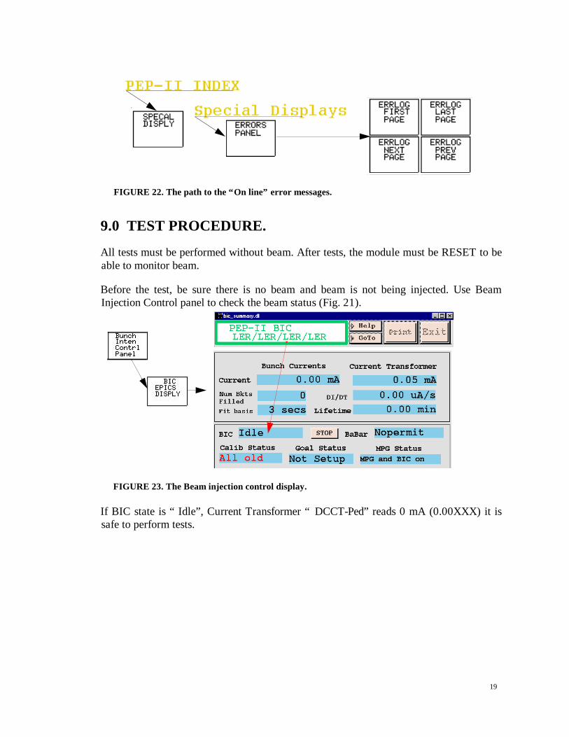
FIGURE 22. The path to the “On line” error messages.
9.0 TEST PROCEDURE.
All tests must be performed without beam. After tests, the module must be RESET to beable to monitor beam.
Before the test, be sure there is no beam and beam is not being injected. Use BeamInjection Control panel to check the beam status (Fig. 21).
FIGURE 23. The Beam injection control display.
If BIC state is “ Idle”, Current Transformer “ DCCT-Ped” reads 0 mA (0.00XXX) it issafe to perform tests.
20
9.1 X and Y beam position offset simulation and trigger status test.
To perform the test, follow the instructions below (Fig. 24).1. Select test to start from, for example “ Select 1&2 Xt”.2. Push “ GO” button. The boards 1 and 2 are selected. X test is set.3. Select “ Setup attenuation panel”.4. Set A attenuator to 8 dB, B to 0 dB.5. Return to the BOAT panel: click on “ ... BOAT BPM Panel”.6. Check 1&2X+ and 1&2X- trigger status and write it to a test table (Tab. 10, LER; Tab.11, HER).7. On the BOAT panel, check attenuators status.8. Click “ ANALOG STATUS DIAG” button.9. Check BRD1_DIF and BRD2_DIF data and write them to a test table.10. Go back to attenuators panel.11. Set A attenuator to 10 dB.12. Repeat steps 5 to 9.13. Set A attenuator to 12 dB.14. Repeat steps 5 to 9.Test is completed.15. Click “ Reset” button
In this test the “ Board 1&2 X-” status indicator should go to a trip state at 10 dB or 12 dBattenuation. See an example below (Fig. 22).
FIGURE 24. An example of the X position offset simulation and trigger status test.
To complete all tests, follow to the steps in the Test Tables Tab. 10 and Tab. 11, seecalibration examples in Tab. 12 and Tab 13 (in the attachment).
ATTENUATORS
CHECK SIMULATED BEAM POSITION
2 3
4 6 8
9
5
1
check
7
STATUS
CHECK
21
Calculated X and Y position offsets at 8 dB, 10 dB and 12 dB attenuations are +-14.7mm, +-18.4 mm and +-22 mm respectively. The “ delta” |∆| on the Test Table is thedifference between calculated (Pcalc) and measured (Pmsr) position,
|∆|=|Pcalc-Pmsr|.
According to the requirements (4.0, 8) the “ delta” should be in a range +- 2 mm.
By monitoring trigger, position and threshold signals from the BOAT BPM module frontpanel, it can be determined, that at 8 dB attenuation, the signal is approximately 1.47 V +-small offset. Between 10 dB and 12 dB attenuation (1.84V and 2.2 V respectively) thethreshold level should be crossed and the trigger signal should change state.
There should never be a trigger at 8 dB attenuation or less, there should always be atrigger at 12 dB attenuation or more. Due to individual logrf boards offset, the triggersignal could trip at 10 dB attenuation.
9.2 “ Select board” test.
The “ Select board” is a single daughter board functionality test. A daughter boards 5 and6 tests include dX/dt and dI/dt tests respectively. Test procedure is the same as in part6.1.
First, set attenuators to A = B = 0 dB. “ Buttons Signals Difference” and “ Buttons SignalsSum” appear on “ Analog Status” panel (Fig. 10). The DIF signal should be from 0V to +-0.19 V, the SUM should be between -1.4 V and -1.6 V, depending on the board offset. Tosimulate different offsets, step A attenuation from 30 dB to 0 dB with B = 0 dB, then withA = 0 dB step B from 0 dB to 30 dB. The suggested step is 6 dB, starting from 0 dBattenuation. The monitored “ difference” and “ sum” signal are inverted. The measuredvalues should be symmetrical to one at A=B=0 dB in the range between +- 3.5 V (Fig.15). The SUM value should be maximal at A=B=0 dB.
FIGURE 25. “ Buttons Signals Difference” values distribution at different test signal attenuation.
The “ Current” data (if board 6 is selected) maximum value should be observed at A = B =0 dB.
When testing the board 6, the Current (“ Board 6 I”) trigger status “high” state meansbeam current is > 100 mA, Low state - beam current is < 100 mA. The dI/dt trigger statuschanges state to “ trip” if a current drop equivalent to 20 mA or more is simulated. Seepart 6.1.
A = B = 0 dB - board offset
22
9.3 RESET.
WARNING: Do not forget to RESET module after the test.
After RESET, module is ready to monitor beam or to proceed to another test.
10.0 TEST SOFTWARE CODE.IDOM - 16 channels:4 bits - [0 to 3], [*] - * bit number 1111 / 0000 Reset, pulse type 0001 select board 1 0010 select board 2 0011 select board 3 0100 select board 4 0101 select board 5 0110 select board 6 1000 select boards 1&2; X test 1001 select boards 1&2; Y test 1010 select boards 3&4; X test 1011 select boards 3&4; Y test4 bits - [4 to 7] Attenuator A data4 bits - [8 to 11] Attenuator B data4 bits - spare
SAM - 16 channels:boards 1 to 5 sum [inputs A1-A10], channels [0 - 4] difference [inputs B1 - B10], channels [6 - 10]
23
board 6 current [inputs B11 and B12], channel [11]spare channel [5] spare [A11, A12] channel [12] free [C1, C2]power status channel [13] +5 V analog [C3, C4] channel [14] -5 V analog [C5, C6] channel [15] +5 V digital [C7, C8]
11.0 MAINTENANCE.
Every month (or more often) maintenance recommendations: to calibrate LER and HERBOAT BPM; to check trip thresholds; to check that BATS bypass trigger status is“UNBYPSSD” (Orbit Change X, Orbit Change Y, dI/dt or Single Bunch, Current Limit) .In the case of the BOAT BPM module malfunction, replace it with the MaintenanceBOAT BPM module (MBOAT).
11.1 Maintenance BOAT BPM module modifications for LER or HER.
11.1.1 Mother board modifications.
The MBOAT module mother board is assembled to use for LER. To modify it for HER, the resistors R4, R5, R6, R116 should be replaced according to the schematic. The values are shown below (Tab. 1).
TABLE 9. BOAT BPM mother board resistors values for LER and HER modules.
11.1.2 Additional modifications
Before the replacement of the malfunctioning module with the MBOAT module, insertthe daughter boards (from the malfunctioning module) in the corresponding MBOATmother board slots. If one of the daughter boards is broken, replace it with spare one.
To replace the linear RF daughter board, modify the gain of the spare one according tothe schematic.
Resistor reference designator
Resistor value for LER, Ω
Resistor value for HER, Ω
R4 619 931R5 619 931R6 619 931R116 931 619
24
The “Single Bunch” shelf should be disconnected from the malfunctioning module,installed on the MBOAT module, connected to the input cables and to the mother board asit was in the malfunctioning module (according to the Single Bunch installation diagramand schematic).
Take replaced module to test bench. Test it with LabView program, use file:boat_test3.vi.
12.0 CONCLUSION.
The BOAT BPM concept, functionality and location are described in chapter 1. Chapters2, 3 and 4 have brief introductions to logrf, linrf, Single Bunch and mother boards.Descriptions which help to understand the software interface, to check the BOAT BPMstatus and to perform test procedure are in chapters 6, 7 and 8. The requirements, chapter5, is squeezed between the hardware and software parts. Chapters 9 10 and 11 are Testprocedure, Test Software Code and Maintenance respectively.