Research Inventy: International Journal of Engineering And Science Vol.6, Issue 1 (January 2016), PP -01-09 Issn (e): 2278-4721, Issn (p):2319-6483, www.researchinventy.com 1 Boost Inverter Circuit with a Coupled Inductor Using Renewable Energy Source B Rajesh*,P Ananda Mohan** Department of EEE, SreeDattha Institute of Engineering & Science Abstract: Renewable power systems often experience big changes in generating output due to fluctuations of energy resources. A boost converter is added to step up the dc voltage when the energy resources are at a weak point. When a very high boost gain is demanded, it experiences serious reverse-recovery problemsdue to large duty cycles. This paper proposes a coupled inductor,by employing a coupled inductor in the circuit and proper adjustment of shoot-through state of a three-phase inverter the converter can realize higher boost gain and a stable ac output voltsge. Finally, the simulation using matlab/simulink results are presented in the paper. Index Terms: Boost inverter, coupled inductor, shoot-through zero state. I. Introduction The increasing tension on the global energy supply has resulted in greater interest in renewable energy resources [1]. This presents a significant opportunity for distributed power generation (DG) systems using renewable energy resources, including wind turbines, photovoltaic (PV) generators, small hydro systems, and fuel cells [2]–[4]. However, these DG units produce awide range of voltages due to the fluctuation of energy resources and impose stringent requirements for the inverter topologies and controls [5]. Usually, a boost-type dc–dc converter is added in the DG units to step up the dc voltage [6] –[8]. This kind of topology, although simple may not be able to provide enough dc voltage gain when the input is very low, even with an extreme duty cycle. Also, large duty cycle operation may result in serious reverse-recovery problems and increase the ratings of switching devices. Furthermore, the added converter may deteriorate system efficiency and increase system size, weight, and cost. On the other hand, the upper and lower devices of the same phase leg cannot be gated on simultaneously in conventional voltage source inverter (VSI). Otherwise, shoot-through problems would occur and destroy the switching devices. Dead time is always used in case of shoot-through events in bridge type converters, but it will cause waveform distortion. Though dead-time compensation technology [9], [10] has been developed, it increases control complexity. So, it is desirable to have a single-stage high-gain boost inverter featuring no shoot through issues. Single-stage topologies, which integrate performance of each stage in a multistage power converter, are becoming the focus of research. Though they may cause increased control complexity, they may offer higher efficiency, reliability, and lower cost. It is observed that many single- stage voltage source [11]–[13] and current source [14], [15] inverters have been proposed. A Z-source inverter (ZSI) proposed in [16] is able to overcome the problems in conventional VSI and conventional current source inverter. It can provide a wide range of obtainable voltage and has been applied to renewable power generation systems [17]–[19]. However, this topology is complex and inductors and capacitors in the Z-network should have high consistency. Moreover, only shoot-through zero state can be regulated when higher voltage gain is required. Widening shoot-through zero state will decrease modulation index and output voltage amplitude. Also, in order to completely avoid the unwanted operation modes, the input diode should be replaced by a switch which turns ON during all active states and traditional zero states [20]. Four quasi-Z-source inverters (qZSIs) derived from the conventional ZSI have been proposed in [21], whose basic principles are similar to those of conventional ZSI. Corresponding control methods and application conditions of conventional ZSI also fit for the qZSIs in theory. Anderson and Peng [21] show some advantages of qZSIs over conventional ZSI, such as lower voltage/current stress of impedance network and lower switch voltage stress. Nevertheless, they do not overcome the limits of conventional ZSI described earlier. This paper presents a novel single-stage boost inverter with a unique impedance network including coupled inductor. The bus voltage can be stepped up by using shoot-through zero state to store and transfer energy within the impedance network. Just as with ZSI, the single-stage boost inverter completely avoids destroying devices during shoot-through zero states. So, it has improved reliability. Second, the inductors and capacitors do not have to be of high consistency, leading to easier circuit parameters design. Third, both shoot-through zero states and coupled inductor’s turn ratio can be regulated to control the boost gain.So, the output voltage can be regulated in a wide range and can be stepped up to a higher value. Finally, the bus voltage equals the sum of the capacitor voltages, and it is higher than each capacitor voltage. This ensures status capacitor voltage ratings can be fully utilized. The single-stage boost inverter with coupled inductor is suitable for applications where the input voltage varies from a relative low level to a higher level continuously while outputting a stable ac voltage.
Transcript
Research Inventy: International Journal of Engineering And Science
Boost Inverter Circuit with a Coupled Inductor Using Renewable
Energy Source
B Rajesh*,P Ananda Mohan** Department of EEE, SreeDattha Institute of Engineering & Science
Abstract: Renewable power systems often experience big changes in generating output due to fluctuations of
energy resources. A boost converter is added to step up the dc voltage when the energy resources are at a weak
point. When a very high boost gain is demanded, it experiences serious reverse-recovery problemsdue to large
duty cycles. This paper proposes a coupled inductor,by employing a coupled inductor in the circuit and proper
adjustment of shoot-through state of a three-phase inverter the converter can realize higher boost gain and a
stable ac output voltsge. Finally, the simulation using matlab/simulink results are presented in the paper.
Index Terms: Boost inverter, coupled inductor, shoot-through zero state.
I. Introduction The increasing tension on the global energy supply has resulted in greater interest in renewable energy
resources [1]. This presents a significant opportunity for distributed power generation (DG) systems using
renewable energy resources, including wind turbines, photovoltaic (PV) generators, small hydro systems, and
fuel cells [2]–[4]. However, these DG units produce awide range of voltages due to the fluctuation of energy
resources and impose stringent requirements for the inverter topologies and controls [5]. Usually, a boost-type
dc–dc converter is added in the DG units to step up the dc voltage [6]–[8]. This kind of topology, although
simple may not be able to provide enough dc voltage gain when the input is very low, even with an extreme
duty cycle. Also, large duty cycle operation may result in serious reverse-recovery problems and increase the
ratings of switching devices. Furthermore, the added converter may deteriorate system efficiency and increase
system size, weight, and cost. On the other hand, the upper and lower devices of the same phase leg cannot be
gated on simultaneously in conventional voltage source inverter (VSI). Otherwise, shoot-through problems
would occur and destroy the switching devices. Dead time is always used in case of shoot-through events in
bridge type converters, but it will cause waveform distortion. Though dead-time compensation technology [9],
[10] has been developed, it increases control complexity. So, it is desirable to have a single-stage high-gain
boost inverter featuring no shoot through issues. Single-stage topologies, which integrate performance of each
stage in a multistage power converter, are becoming the focus of research. Though they may cause increased
control complexity, they may offer higher efficiency, reliability, and lower cost. It is observed that many single-
stage voltage source [11]–[13] and current source [14], [15] inverters have been proposed. A Z-source inverter
(ZSI) proposed in [16] is able to overcome the problems in conventional VSI and conventional current source
inverter. It can provide a wide range of obtainable voltage and has been applied to renewable power generation
systems [17]–[19]. However, this topology is complex and inductors and capacitors in the Z-network should
have high consistency. Moreover, only shoot-through zero state can be regulated when higher voltage gain is
required. Widening shoot-through zero state will decrease modulation index and output voltage amplitude. Also,
in order to completely avoid the unwanted operation modes, the input diode should be replaced by a switch
which turns ON during all active states and traditional zero states [20]. Four quasi-Z-source inverters (qZSIs)
derived from the conventional ZSI have been proposed in [21], whose basic principles are similar to those of
conventional ZSI. Corresponding control methods and application conditions of conventional ZSI also fit for the
qZSIs in theory. Anderson and Peng [21] show some advantages of qZSIs over conventional ZSI, such as lower
voltage/current stress of impedance network and lower switch voltage stress. Nevertheless, they do not
overcome the limits of conventional ZSI described earlier. This paper presents a novel single-stage boost
inverter with a unique impedance network including coupled inductor. The bus voltage can be stepped up by
using shoot-through zero state to store and transfer energy within the impedance network. Just as with ZSI, the
single-stage boost inverter completely avoids destroying devices during shoot-through zero states. So, it has
improved reliability. Second, the inductors and capacitors do not have to be of high consistency, leading to
easier circuit parameters design. Third, both shoot-through zero states and coupled inductor’s turn ratio can be
regulated to control the boost gain.So, the output voltage can be regulated in a wide range and can be stepped up
to a higher value. Finally, the bus voltage equals the sum of the capacitor voltages, and it is higher than each
capacitor voltage. This ensures status capacitor voltage ratings can be fully utilized. The single-stage boost
inverter with coupled inductor is suitable for applications where the input voltage varies from a relative low
level to a higher level continuously while outputting a stable ac voltage.
Boost inverter circuit with a coupled inductor using Renewable energy source
2
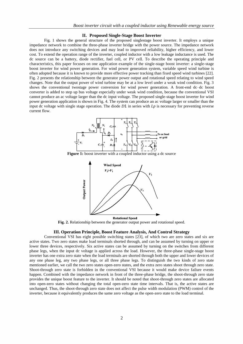
II. Proposed Single-Stage Boost Inverter Fig. 1 shows the general structure of the proposed singlestage boost inverter. It employs a unique
impedance network to combine the three-phase inverter bridge with the power source. The impedance network
does not introduce any switching devices and may lead to improved reliability, higher efficiency, and lower
cost. To extend the operation range of the inverter, coupled inductor with a low leakage inductance is used. The
dc source can be a battery, diode rectifier, fuel cell, or PV cell. To describe the operating principle and
characteristics, this paper focuses on one application example of the single-stage boost inverter: a single-stage
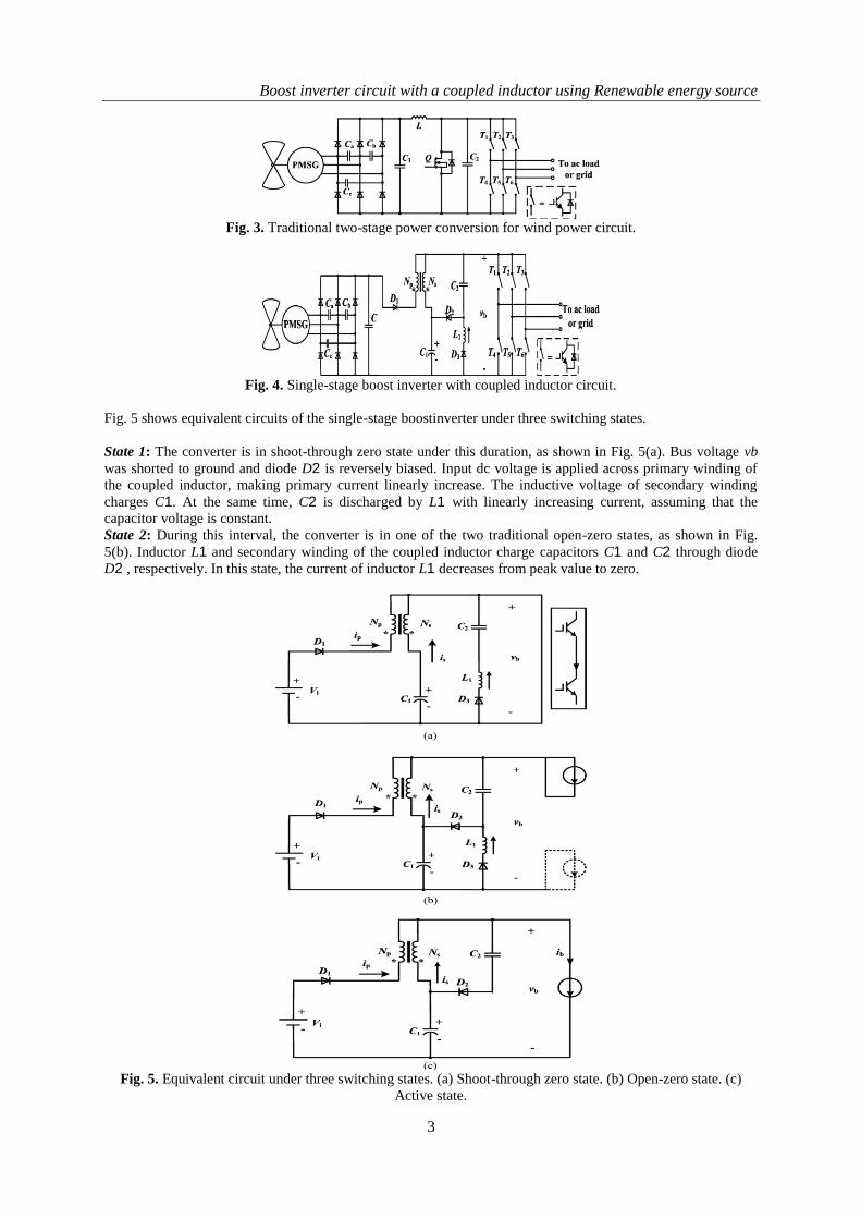
boost inverter for wind power generation. For wind power generation system, variable speed wind turbine is
often adopted because it is known to provide more effective power tracking than fixed speed wind turbines [22].
Fig. 2 presents the relationship between the generator power output and rotational speed relating to wind speed
changes. Note that the output power of wind turbine may be at a low level under a weak wind condition. Fig. 3
shows the conventional twostage power conversion for wind power generation. A front-end dc–dc boost
converter is added to step up bus voltage especially under weak wind condition, because the conventional VSI
cannot produce an ac voltage larger than the dc input voltage. The proposed single-stage boost inverter for wind
power generation application is shown in Fig. 4. The system can produce an ac voltage larger or smaller than the
input dc voltage with single stage operation. The diode D1 in series with Lp is necessary for preventing reverse
current flow.
Figure 1: boost inverter with a coupled inductor using a dc source
Fig. 2. Relationship between the generator output power and rotational speed.
III. Operation Principle, Boost Feature Analysis, And Control Strategy Conventional VSI has eight possible switching states [23], of which two are zero states and six are
active states. Two zero states make load terminals shorted through, and can be assumed by turning on upper or
lower three devices, respectively. Six active states can be assumed by turning on the switches from different
phase legs, when the input dc voltage is applied across the load. However, the three-phase single-stage boost
inverter has one extra zero state when the load terminals are shorted through both the upper and lower devices of
any one phase leg, any two phase legs, or all three phase legs. To distinguish the two kinds of zero state
mentioned earlier, we call the two zero states open-zero states, and the extra zero states shoot through zero state.
Shoot-through zero state is forbidden in the conventional VSI because it would make device failure events
happen. Combined with the impedance network in front of the three-phase bridge, the shoot-through zero state
provides the unique boost feature to the inverter. It should be noted that shoot-through zero states are allocated
into open-zero states without changing the total open-zero state time intervals. That is, the active states are
unchanged. Thus, the shoot-through zero state does not affect the pulse width modulation (PWM) control of the
inverter, because it equivalently produces the same zero voltage as the open-zero state to the load terminal.
Boost inverter circuit with a coupled inductor using Renewable energy source
3
Fig. 3. Traditional two-stage power conversion for wind power circuit.
Fig. 4. Single-stage boost inverter with coupled inductor circuit.
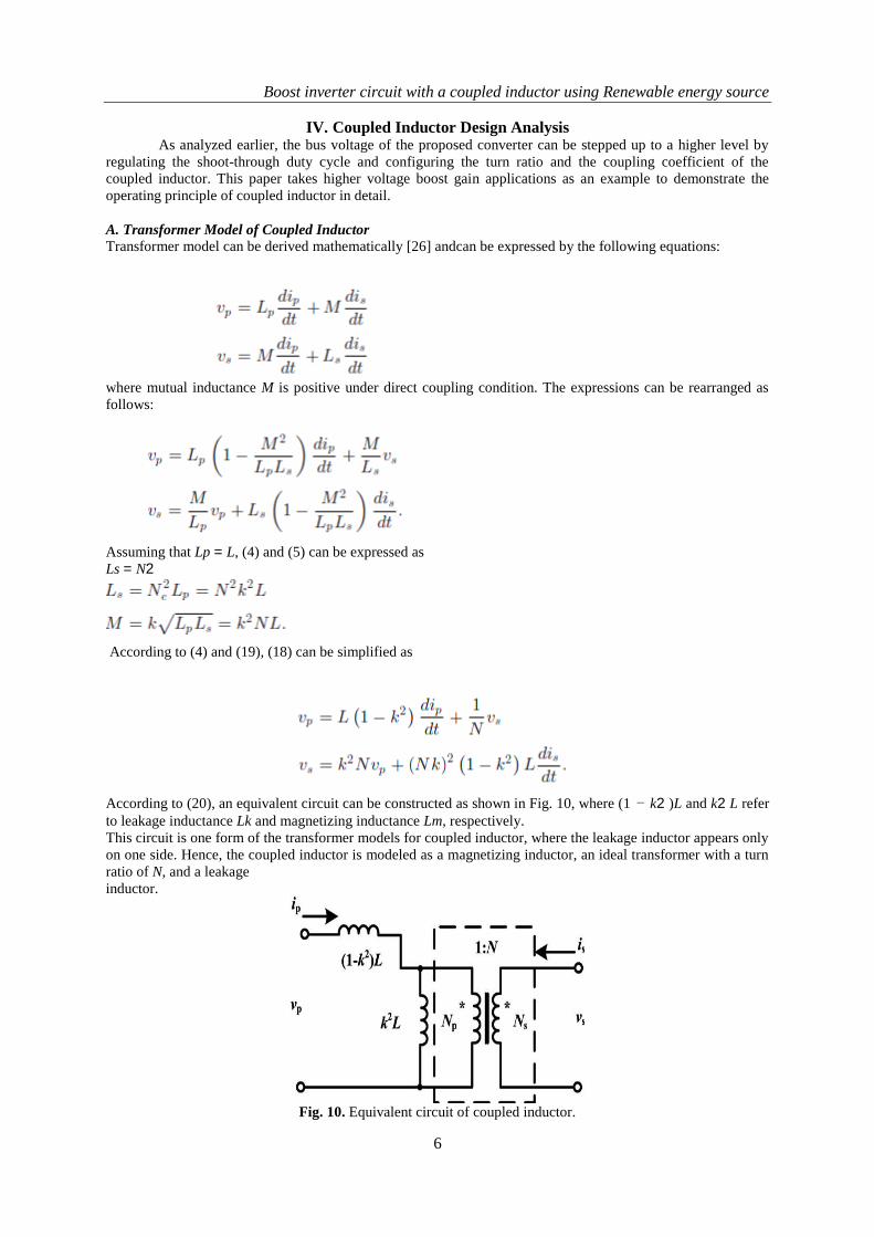
Fig. 5 shows equivalent circuits of the single-stage boostinverter under three switching states.
State 1: The converter is in shoot-through zero state under this duration, as shown in Fig. 5(a). Bus voltage vb
was shorted to ground and diode D2 is reversely biased. Input dc voltage is applied across primary winding of
the coupled inductor, making primary current linearly increase. The inductive voltage of secondary winding
charges C1. At the same time, C2 is discharged by L1 with linearly increasing current, assuming that the
capacitor voltage is constant.
State 2: During this interval, the converter is in one of the two traditional open-zero states, as shown in Fig.
5(b). Inductor L1 and secondary winding of the coupled inductor charge capacitors C1 and C2 through diode
D2 , respectively. In this state, the current of inductor L1 decreases from peak value to zero.
Fig. 5. Equivalent circuit under three switching states. (a) Shoot-through zero state. (b) Open-zero state. (c)
Active state.
Boost inverter circuit with a coupled inductor using Renewable energy source
4
State 3: When the circuit is in one of the six active states, as shown in Fig. 5(c), diode D3 is reverse biased. The
energy stored in the coupled inductor and C1 releases to the load, and the bus voltage is stepped up to a higher
level.
Two boost modes can be achieved by regulating the shootthrough zero state as well as configuring the
turn ratio and coupling coefficient of the coupled inductor. Operating principle of the single-stage boost inverter
is analyzed under these two modes. When applying the converter to voltage drop compensation or applications
where lower boost gain is needed, the inductance of coupled inductor should be designed large enough to ensure
its continuous current-mode operation. When higher boost gain is required, the inductance of the primary
winding Lp should be as small as to keep the circuit working in discontinuous current mode. Fig. 6 shows
coupled inductor current waveform in one shoot-through period Tsh under two operation modes, respectively.
Note that the shoot-through period Tsh is the equivalent switching period viewed from the impedance network,
which is not equivalent to the switching period Ts of the inverter bridge. Tsh may be two or six times of Ts ,
determined by the modulation scheme it used [16], [24], [25], which reduces the required size and weight of the
coupled inductor
Fig. 6. Coupled inductor current waveforms under two operation modes. (a)Inductor Lp works in CCM. (b)
Inductor Lp works in DCM.
A. Lower Voltage Boost Gain Mode
In lower voltage boost gain applications, the key characteristic is that the current through Lp generally works in
continuous mode, as shown in Fig. 6(a).
Define the shoot-through duty cycle D0 as the time when the three-phase bridge is in shoot-through state, and
the duty cycle 1 − D0 as the time when the three-phase bridge is in nonshootthrough state, the average voltage
across the primary winding during one shoot-through period can be expressed as
(vLp (t))Tsh CCM
Tsh = D0Vi + (1 − D0) (Vi − vb) = 0. (1)
From (1), the amplitude of bus voltage can be expressed as follows:
(2)
Define B as the boost gain,B = _vbVi , which can be expressed as
(3)
The boost gain is similar to that of conventional dc–dc boost converter in this boost mode.
B. Higher Voltage Boost Gain Mode
In higher voltage boost gain applications, the key characteristic is that the inductance of primary winding is less
than that of secondary winding, and primary winding current generally works in discontinuous mode, as shown
in Fig. 6(b).
Define the coupling coefficient as
Boost inverter circuit with a coupled inductor using Renewable energy source
5
where Lp , Ls , and M are the self-inductance of each winding and the mutual inductance, and the effective turn
ratio
Define the duty cycle D1 as the time when the inductor Lp current decreasing from peak value to zero, the
average voltage across the both sides of coupled inductor during one shoot-through period can be expressed as
From (6) and (7), the amplitude of bus voltage can be expressed as
Define physical turn ratio of ideal transformer as N = Ns /Np .According to the relationship of Ne and N: Ne = N
× k, (8) canbe simplified as
The output peak phase voltage ˆvac generated by the inverter can be expressed as
All the traditional PWM schemes can be used to control the inverter. Fig. 9 shows the maximum
constant boost control method with third-harmonic injection [25]. The equivalent dcbus voltage is boosted
because of the shoot-through zero states. Shooting through three phase legs at the same time can reduce the
current stress of each device, while the switching frequency is doubled. Meanwhile, the shoot-through states
should preferably have the same time duration to minimize the size of the impedance network. When the
modulation index m is set, the shoot-through duty cycle D0 versus modulation index m can be expressed as
follows:
So, the maximum shoot-through duty cycle is limited by modulation index. When the modulation index is set to
no less than 0.8, the shoot-through duty cycle is limited to 0.307.
Fig. 9. Maximum constant boost control method with third-harmonic injection.
Boost inverter circuit with a coupled inductor using Renewable energy source
6
IV. Coupled Inductor Design Analysis As analyzed earlier, the bus voltage of the proposed converter can be stepped up to a higher level by
regulating the shoot-through duty cycle and configuring the turn ratio and the coupling coefficient of the
coupled inductor. This paper takes higher voltage boost gain applications as an example to demonstrate the
operating principle of coupled inductor in detail.
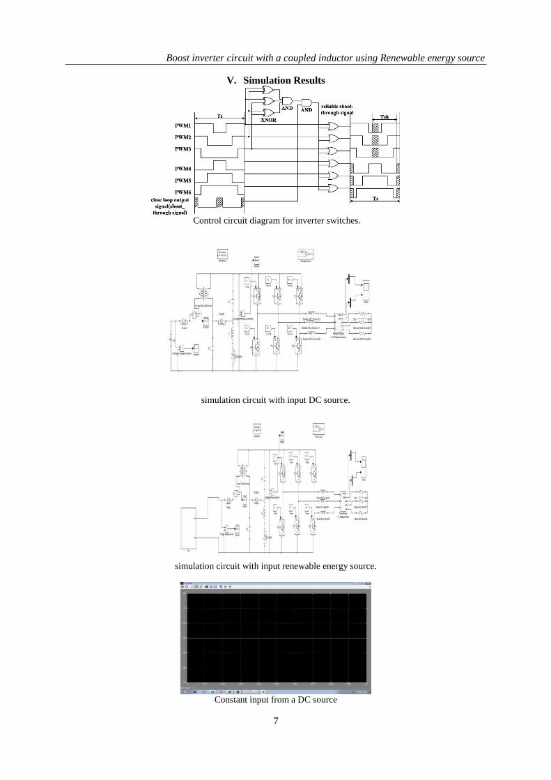
A. Transformer Model of Coupled Inductor
Transformer model can be derived mathematically [26] andcan be expressed by the following equations:
where mutual inductance M is positive under direct coupling condition. The expressions can be rearranged as
follows:
Assuming that Lp = L, (4) and (5) can be expressed as
Ls = N2
According to (4) and (19), (18) can be simplified as
According to (20), an equivalent circuit can be constructed as shown in Fig. 10, where (1 − k2 )L and k2 L refer
to leakage inductance Lk and magnetizing inductance Lm, respectively.
This circuit is one form of the transformer models for coupled inductor, where the leakage inductor appears only
on one side. Hence, the coupled inductor is modeled as a magnetizing inductor, an ideal transformer with a turn
ratio of N, and a leakage
inductor.
Fig. 10. Equivalent circuit of coupled inductor.
Boost inverter circuit with a coupled inductor using Renewable energy source
7
V. Simulation Results
Control circuit diagram for inverter switches.
simulation circuit with input DC source.
simulation circuit with input renewable energy source.
Constant input from a DC source
Boost inverter circuit with a coupled inductor using Renewable energy source
8
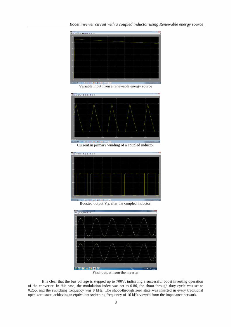
Variable input from a renewable energy source
Current in primary winding of a coupled inductor
Boosted output Vab after the coupled inductor.
Final output from the inverter
It is clear that the bus voltage is stepped up to 700V, indicating a successful boost inverting operation
of the converter. In this case, the modulation index was set to 0.86, the shoot-through duty cycle was set to
0.255, and the switching frequency was 8 kHz. The shoot-through zero state was inserted in every traditional
open-zero state, achievingan equivalent switching frequency of 16 kHz viewed from the impedance network.
Boost inverter circuit with a coupled inductor using Renewable energy source
9
VI. Conclusion This paper has presented a novel single-stage boost inverter with coupled inductor, which exhibits several
merits.
1) It employs a unique impedance network including coupled inductor to connect the three-phase inverter
bridge to the power source. By designing the coupled inductor properly and adjusting the previously
forbidden shoot-through zero state, the magnitude of the bus voltage can be greatly stepped up.
2) By configuring turn ratio and coupling coefficient of the coupled inductor differently, the impedance
network can work in two boost modes making it suitable for different inverting applications.
3) Shoot-through states, which are forbidden in conventional VSIs, are utilized to store and transfer energy
within the impedance network to boost the amplitude of the bus voltage. Waveform distortion of the ac
output voltage caused by dead time is essentially avoided.
References [1]. T. Kerekes, M. Liserre, R. Teodorescu, and C. Klumpner, “Evaluation of three-phase transformerless photovoltaic
inverter topologies,” IEEE Trans. Power Electron., vol. 24, no. 9, pp. 2202–2211, Sep. 2009.
[2]. B. Yang, W. Li, Y. Zhao, and X. He, “Design and analysis of a gridconnected photovoltaic power system,” IEEE
Trans. Power Electron.,vol. 25, no. 4, pp. 992–1000, Apr. 2010.
[3]. G. Zhu and K. Wang, “Modeling and design considerations of coupled inductor converters,” in Proc. IEEE Appl.
Power Electron. Conf., 2010,pp. 7–13
[4]. S. H. Hosseini, S. Danyali, and A. Y. Goharrizi, “Single stage single phase series-grid connected PV system for
voltage compensation and power supply,” in Proc. IEEE Power Energy Soc. Gen. Meet., 2009, pp. 1–7.
[5]. B. Sahan, A. N. Vergara, N. Henze, A. Engler, and P. Zacharias, “A singlestage PVmodule integrated converter
based on a low-power current-source inverter,” IEEE Trans. Ind. Electron., vol. 55, no. 7, pp. 2602–2609, Jul.2008.