Comparison of Silicon, Germanium and Diamond sensors for Using it in HEP Detector Applications 1 2/16/2017 Advanced Detectors for Nuclear, High Energy and Astroparticle Physics Bose Institute Kolkata Shyam Kumar 1 , Raghava Varma 1 , K.Das Gupta 1 , Pradeep Sarin 1 , S.K. Deb 2 Department of Physics, IIT Bombay, Mumbai 1 CRNTS, IIT Bombay, Mumbai 2 Email: [email protected]Thanks for ALICE Utilization and Upgrade Project and IRCC, IIT Bombay for Support 15-17 February 2017
Transcript
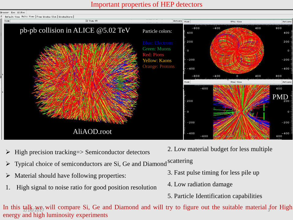
Comparison of Silicon, Germanium and Diamond
sensors for Using it in HEP Detector Applications
12/16/2017
Advanced Detectors for Nuclear, High Energy and Astroparticle Physics
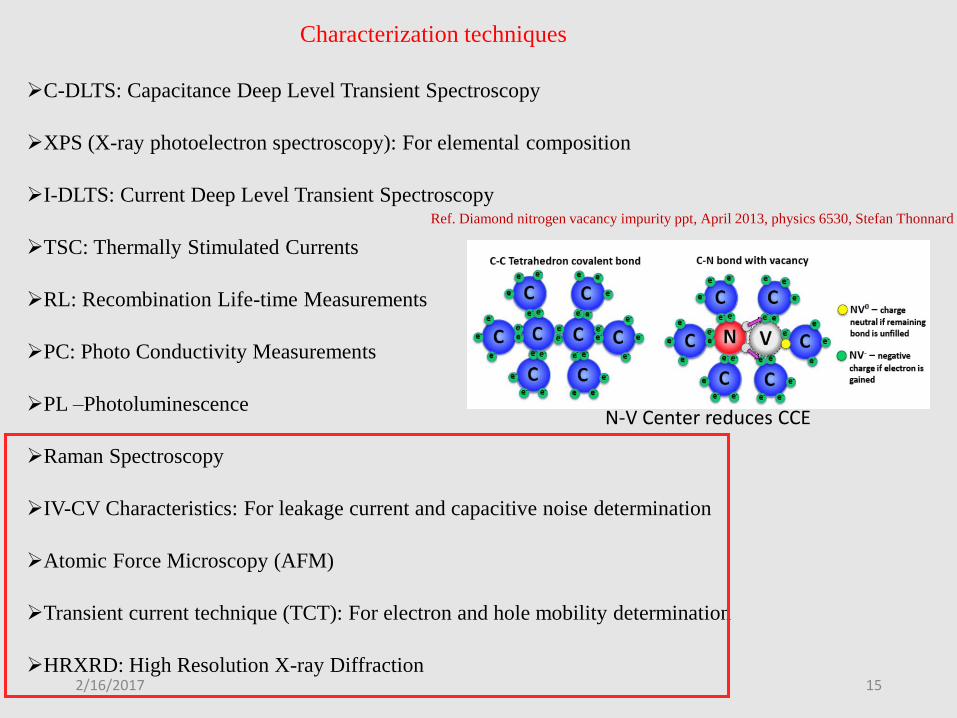
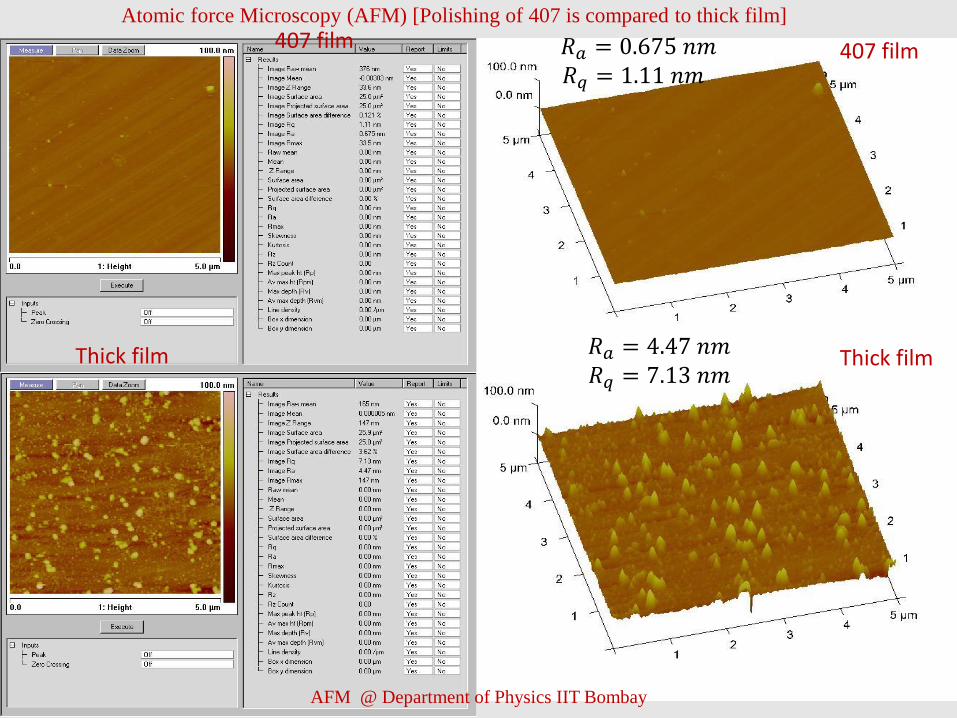
High Resolution XRD @ Department of Physics IIT Bombay
Raman Spectroscopy @ CRNTS, IIT Bombay
2 𝜃 =119.4432 𝜃 =119.443
Diamond film shows the good XRD and Raman spectrum
2/16/2017 17
800 1000 1200 1400 1600 1800 2000 2200 2400 2600
0
2000
4000
6000
8000
10000
12000
14000
16000
Inte
nsity
(a.u
.)
Energy Shift (per cm)
Sample: 407
Ohmic Contact: Thermal Evaporation (Both side)
Cr/Au: 20 nm/100 nm
Slow Annealing of the sample up to 605 K
Sample 407 : 5.0 × 5.0 × 0.4 𝑚𝑚3
Sample 407
Thick film
Resistance = 1.3 × 10¹⁴ Ω
Resistance = 2.5 × 10¹⁴ Ω
I-V done at BARC, Thanks to Amit and Dr. Anita
Topkar (Electronics division BARC)
Contact made @ CEN, IIT Bombay
Diamond peak at 1332 𝑐𝑚−1
Red Laser =632.8 nm
I-V looking promising
𝜌 = 2 × 10¹¹Ω𝑚
𝜌 = 2.5 × 10¹¹Ω𝑚
2/16/2017 18
Transient Current Technique (TCT) measurement for diamond
𝐴𝑚241- 𝛼 source of energy, 5486 KeV (85%), 5443 KeV (13%) and 5388 KeV (1%)
Range of 𝛼 in Material: Fluka simulation (Ionizing Energy Loss (IEL))
Bragg’s Peak
Curve highly useful in cancer treatment (Medical Applications)
Diamond
IEL ≈ 5485.9 KeV
NIEL ≈ KeV
Signal=5485900/13.6
=403375 e-h pairs
300 𝜇𝑚 thick material
𝛼
Experimental measurement:
3.5× 3.5 × 0.4 𝑚𝑚3 diamond (IIA technologies)
𝛼 will stop with in 15 𝜇𝑚 of diamond
Silicon
IEL ≈ 5485.9 KeV
NIEL ≈ KeV
Signal=5485900/3.6
= 1523861 e-h pairs
Germanium
IEL ≈ 5485.8 KeV
NIEL ≈ KeV
Signal=5485800/2.96
= 18,53311 e-h pairs
Gain of cividec amplifier= +40 dB =>𝑣𝑜𝑢𝑡
𝑣𝑖𝑛= 100
𝑣𝑜𝑢𝑡 = 100 𝑣𝑖𝑛 = 100 × 50 Ω × 𝐼𝑖𝑛
𝐼𝑖𝑛(𝑚𝐴) =𝑣𝑜𝑢𝑡 (𝑚𝑉)
5000
𝑄𝑐𝑜𝑙𝑙𝑒𝑐𝑡𝑒𝑑 = 𝐼𝑖𝑛 𝑑𝑡
𝝐 = 𝟐. 𝟕𝟑 𝑬𝒈 + 𝟎. 𝟓𝟓 𝒆𝑽
Ref: Electron-Hole-Pair Creation
Energies in Semiconductors ,
PRL, Volume 35, Number 32
2/16/2017 19
𝐶𝐶𝐸 =𝑄𝑐𝑜𝑙𝑙𝑒𝑐𝑡𝑒𝑑
𝑄𝑐𝑟𝑒𝑎𝑡𝑒𝑑×100 =
𝑄𝑐𝑜𝑙𝑙𝑒𝑐𝑡𝑒𝑑
403375×100
Cividec Amplifier CERN, used for testing
Timing of diamond pulse of the order of ns
2/16/2017 20
Summary and Future Plan
Diamond has good signal to noise ratio, fast timing, low material budget, low radiation damage
and good particle identification capabilities, so it will be a good choice for HEP experiments
Diamond has large e-h pair creation energy so less disturbance in charge center of gravity
Diamond can also be used for the detection of slow and fast neutrons
We have grown diamond film up to 1 mm thickness it has nitrogen, I will do cutting and
polishing and will test again
We have also tested good quality diamond from IIA technologies
The only problem with diamond we don’t have large area high quality diamond
Still working on growing high quality diamond in Lab
2/16/2017 21Thank You !!!
FLUKA Simulation used Ref : "FLUKA: a multi-particle transport code"A. Ferrari, P.R. Sala, A. Fasso`, and J. Ranft,CERN-2005-10 (2005), INFN/TC_05/11, SLAC-R-773
2/16/2017 22
n interacts with 6𝐿𝑖 in 6LiF layer (95%) n directly interact with carbon12C