An IMPORTANT NOTICE at the end of this data sheet addresses availability, warranty, changes, use in safety-critical applications,intellectual property matters and other important disclaimers. PRODUCTION DATA.
BQ24392SLIS146G –JUNE 2012–REVISED SEPTEMBER 2017
BQ24392 Dual SPST USB 2.0 High Speed Switch with USB Battery Charging SpecificationRevision 1.2 Detection
1
1 Features1• USB 2.0 High Speed Switch• Detects USB Battery Charging Specification
Version 1.2 (BCv1.2) Compliant Chargers• Compatible Accessories
– Dedicated Charging Port– Standard Downstream Port– Charging Downstream Port
• Non-Standard Chargers– Apple™ Charger– TomTom™ Charger– USB Chargers Not Compliant With Battery
Charging Specification Version 1.2 (BCv1.2)• –2 V to 28 V VBUS Voltage Range• ESD Performance Tested per JESD 22
– 4000-V Human-Body Model– 1500-V Charged-Device Model (C101)
2 Applications• Mobile Phones• Smart Phones• Cameras• GPS Systems
3 DescriptionThe BQ24392 is a dual single-pole single-throw(SPST) USB 2.0 high-speed isolation switch withcharger detection capabilities for use with micro andmini-USB ports. This USB switch allows mobilephones, tablets, and other battery operatedelectronics to be charged from different adapters withminimal system software. The device’s chargerdetection circuitry can support USB Battery ChargingSpecification version 1.2 (BCv1.2) compliant,Apple™, TomTom™, and other non-standardchargers.
The BQ24392 device is powered through VBUS whena charger is attached to the micro or mini-USB portand has a 28-V tolerance to avoid the need forexternal protection.
Device Information(1)
PART NUMBER PACKAGE BODY SIZE (NOM)BQ24392 UQFN (10) 2.05 mm × 1.55 mm
(1) For all available packages, see the orderable addendum atthe end of the datasheet.
9 Power Supply Recommendations ...................... 1110 Layout................................................................... 12
10.1 Layout Guidelines ................................................. 1210.2 Layout Example .................................................... 13
11 Device and Documentation Support ................. 1411.1 Receiving Notification of Documentation Updates 1411.2 Community Resources.......................................... 1411.3 Trademarks ........................................................... 1411.4 Electrostatic Discharge Caution............................ 14
12 Mechanical, Packaging, and OrderableInformation ........................................................... 14
4 Revision History
Changes from Revision F (July 2017) to Revision G Page
• Changed RON From: 8 Ω TYP To: 3.5 Ω TYP, 6.9 Ω MAX in the Electrical Characteristic table .......................................... 5
Changes from Revision E (February 2017) to Revision F Page
• Changed CHG_DET diode direction from right facing to left facing in Application Schematic. .......................................... 10
Changes from Revision D (January 2016) to Revision E Page
• Changed From: BQ24932 To: BQ24392 in the Description ................................................................................................... 1• Changed From: BQ24932 To: BQ24392 in the Overview ...................................................................................................... 6• Changed title From: Using the BQ24932 GPIOs To: Using the BQ24392 GPIOs................................................................. 9
Changes from Revision C (January 2015) to Revision D Page
• Changed diode direction from left facing to right facing in Application Schematic. ............................................................. 10
Changes from Revision B (October 2014) to Revision C Page
USB switch status indicatorOpen-drain output. 10kΩ external pull-up resistor requiredSW_OPEN = LOW indicates when switch is connectedSW_OPEN = HIGH-Z indicates when then switch is not connected
2 DM_HOST I/O D– signal to transceiver3 DP_HOST I/O D+ signal to transceiver
4 CHG_AL_N O
Charging status indicatorOpen-drain output. 10kΩ external pull-up resistor requiredCHG_AL_N = LOW indicates when charging is allowedCHG_AL_N = HIGH-Z indicates when charging is not allowed
5 GOOD_BAT IBattery status indication from systemGOOD_BAT = LOW indicates a dead batteryGOOD_BAT = HIGH indicates a good battery
6 GND - Ground7 DP_CON I/O D+ signal from USB connector8 DM_CON I/O D– signal from USB connector9 VBUS I Supply pin from USB connector
10 CHG_DET O
Charger detection indicatorPush-Pull output to systemCHG_DET = LOW indicates when a charger is not detectedCHG_DET = HIGH indicates when a charger detected
(1) JEDEC document JEP155 states that 500-V HBM allows safe manufacturing with a standard ESD control process. Manufacturing withless than 500-V HBM is possible with the necessary precautions.
(2) JEDEC document JEP157 states that 250-V CDM allows safe manufacturing with a standard ESD control process. Manufacturing withless than 250-V CDM is possible with the necessary precautions.
6.2 ESD RatingsVALUE UNIT
V(ESD) Electrostatic discharge
Human-body model (HBM), per ANSI/ESDA/JEDEC JS-001 (1) ±4000
VCharged-device model (CDM), per JEDEC specification JESD22-C101 (2) ±1500
IEC Contact discharge pins DP_CON and DM_CON to GND ±8000
7.1 OverviewThe BQ24392 is a USB 2.0 high-speed isolation switch with charger detection capabilities for use with micro andmini-USB ports. Upon plugin of a Battery Charging Specification 1.2 (BCv1.2) compliant, Apple™, TomTom™, orother USB charger into a micro or mini-USB connector, the device will automatically detect the charger andoperate the USB 2.0 high-speed isolation switch.
The BQ24392 device is powered through VBUS when a charger is attached to the micro or mini-USB port andhas a 28-V tolerance to avoid the need for external protection.
Feature Description (continued)When a micro or mini-USB accessory is inserted into the connector and once VBUS is greater than VVBUS_VALIDthreshold, the BQ24392 will enter into the Data Contact Detection (DCD) state which includes a 600-ms timeoutfeature that is prescribed in the USB Battery Charging Specification version 1.2 (BCv1.2). If the micro or mini-USB accessory is determined to be USB BCv1.2 compliant, a 130-ms debounce period will initiate and theBQ24392 will proceed to its primary detection and then secondary detection states to determine if a DedicatedCharging Port (DCP), Standard Downstream Port (SDP), or Charging Downstream Port (CDP) is attached to theUSB-port. The minimum detection time for a DCP, SDP, and CDP is 130 ms, but can be as long as 600 ms dueto the slow plug in effect.
If the GOOD_BAT pin is high, the USB 2.0 switches are automatically closed to enable data transfer after thedevice detects a Standard Downstream Port (SDP) or Charging Downstream Port (CDP) was connected.
If Data Contact Detection (DCD) fails, the BQ24392 proceeds to detect whether an Apple or TomTom chargerwas inserted by checking the voltage level on DP_CON and DM_CON. Thus, for Apple and TomTom chargers,detection time typically takes ~600 ms.
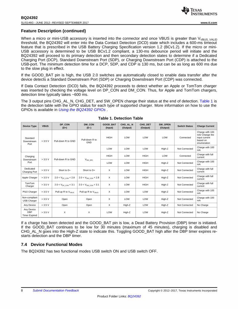
The 3 output pins CHG_AL_N, CHG_DET, and SW_OPEN change their status at the end of detection. Table 1 isthe detection table with the GPIO status for each type of supported charger. More information on how to use theGPIOs is available in Using the BQ24392 GPIOs .
Table 1. Detection Table
Device Type VBUS DP_CON(D+)
DM_CON(D–)
GOOD_BAT(Input)
CHG_AL_N(Output)
CHG_DET(Output)
SW_OPEN(Output) Switch Status Charge Current
StandardDownstream
Port> 3.5 V Pull-down R to GND Pull-down R to
GND
HIGH LOW LOW LOW Connected
Charge with 100mA/ Change theinput currentbased onenumeration
LOW LOW LOW High-Z Not Connected Charge with 100mA
ChargingDownstream
Port> 3.5 V Pull-down R to GND VDM_SRC
HIGH LOW HIGH LOW Connected Charge with fullcurrent
LOW LOW HIGH High-Z Not Connected Charge with 100mA
DedicatedCharging Port
> 3.5 V Short to D– Short to D+ X LOW HIGH High-Z Not Connected Charge with fullcurrent
Apple Charger > 3.5 V 2.0 < VDP_CON < 2.8 2.0 < VDM_CON < 2.8 X LOW HIGH High-Z Not Connected Charge with fullcurrent
TomTomCharger > 3.5 V 2.0 < VDP_CON < 3.1 2.0 < VDM_CON < 3.1 X LOW HIGH High-Z Not Connected Charge with full
current
PS/2 Charger > 3.5 V Pull-up R to VVBUS Pull-up R to VVBUS X LOW LOW High-Z Not Connected Charge with 100mA
Non-compliantUSB Charger
> 3.5 V Open Open X LOW LOW High-Z Not Connected Charge with 100mA
Any Device < 3.5 V Open Open X High-Z LOW High-Z Not Connected No Charge
Any DeviceDBP
Timer Expired> 3.5 V X X LOW High-Z LOW High-Z Not Connected No Charge
If a charge has been detected and the GOOD_BAT pin is low, a Dead Battery Provision (DBP) timer is initiated.If the GOOD_BAT continues to be low for 30 minutes (maximum of 45 minutes), charging is disabled andCHG_AL_N goes into the High-Z state to indicate this. Toggling GOOD_BAT high after the DBP timer expires re-starts detection and the DBP timer.
7.4 Device Functional ModesThe BQ24392 has two functional modes USB switch ON and USB switch OFF.
NOTEInformation in the following applications sections is not part of the TI componentspecification, and TI does not warrant its accuracy or completeness. TI’s customers areresponsible for determining suitability of components for their purposes. Customers shouldvalidate and test their design implementation to confirm system functionality.
8.1 Application Information
8.1.1 Using the BQ24392 GPIOs
8.1.1.1 CHG_AL and CHG_DETThe BQ24392 has 2 charger indicators, CHG_AL_N and CHG_DET, that the host can use to determine whetherit can charge and if it can charge at a low or high current. Table 2 demonstrates how these outputs should beinterpreted. CHG_AL_N is an open drain output and is active when the output of the pin is low. CHG_DET is apush-pull output and is high in the active state.
Table 2. bq24392 Outputs
CHG_AL_N CHG_DET
High-Z X Charging is not allowed
Low Low Low-current charging is allowed
Low High High-current charging is allowed
The system must define what is meant by low-current and high-current charging. If CHG_DET is high, a systemcould try to draw 2 A, 1.5 A, or 1.0 A. If the system is trying to support > 1.5-A chargers, then the system has touse a charger IC that is capable of monitoring the VBUS voltage as it tries to pull the higher current values. If thevoltage on VBUS starts to drop because that high of a current is supported then the system has to reduce theamount of current it is trying to draw until it finds a stable state with VBUS not dropping.
8.1.1.2 SW_OPENSW_OPEN is an open drain output that indicates whether the USB switches are opened or closed. In the High-Zstate the switches are open and in the active, or low state, the switches are closed. The host should monitor thispin to know when the switches are closed or open.
8.1.1.3 GOOD_BATGOOD_BAT is used by the host controller to indicate the status of the battery to the BQ24392. This pin affectsthe switch status for a SDP or CDP, and it also affects the Dead Battery Provision (DBP) timer as discussed inthe Charger Detection section.
8.1.1.4 Slow Plug-in EventAs you insert a charger into the USB receptacle, the pins are configured so that the VBUS and GND pins makecontact first. This presents a problem as the BQ24392 (or any other charger detection IC) requires access to theD+ and D– lines to run detection. This is why the BQ24392 has a standard 130-ms debounce time after VBUSvalid to run the detection algorithm. This delay helps minimize the effects of the D+ and D– lines making contactafter VBUS and GND.
Figure 4 is from the datasheet of a standard male micro-USB connector and shows how the data connections(red line) are slightly recessed from the power connections (blue line).
Figure 4. Data Connections Recessed from Power Connections
However, in some cases the charger is inserted very slowly, causing the VBUS and GND to make contact longbefore D+ and D–. Due to this effect, there is no guaranteed detection time as the detection time can vary basedon how long it takes to insert the charger. If longer than 600 ms is taken to insert the charger into the USBreceptacle, the detection algorithm of the BQ24392 will timeout and instead of the charger being detected as aDCP, it is now detected as a nonstandard charger (D+ and D– floating).
8.2 Typical ApplicationThe BQ24392 device is used between the micro or mini-USB connector port and USB host to enable and disablethe USB data path and detect chargers that are inserted into the micro or mini-USB connector.
Typical Application (continued)8.2.1 Design RequirementsVBUS requires 1μF - 10μF and 0.1-μF bypass capacitors to reduce noise from circuit elements by providing alow impedance path to ground for the unwanted high frequency content. The 0.1-μF capacitor filters out higherfrequencies and has a lower series inductance while the 1μF ~1 0μF capacitor filters out the lower frequenciesand has a much higher series inductance. Using both capacitors will provide better load regulation across thefrequency spectrum.
SW_OPEN and CHG_AL_N are open-drain outputs that require a 10-kΩ pull-up resistor to VDDIO.
VBUS, DM_CON, and DP_CON are recommended to have an external resistor of 2.2-Ω to provide extraballasting to protect the chip and internal circuitry.
DM_CON and DP_CON are recommended to have a 1-pF external ESD protection diode rated for 8-kV IECprotection to prevent failure in case of an 8-kV IEC contact discharge.
VBUS is recommended to have a 1-pF ~ 10-pF external ESD Protection Diode rated for 8-kV IEC protection toprevent failure in case of an 8-kV IEC contact discharge
CHG_DET is a push-pull output pin. An external pull-up and diode are shown to depict a typical 3.3-V system.The pull-up resistor and diode are optional. The pull-up range on the CHG_DET pin is from 3.5 V to VVBUS. WhenVVBUS > 7 V, CHG_DET will be clamped to 7 V.
8.2.2 Detailed Design ProcedureThe minimum pull-up resistance for the open-drain data lines is a function of the pull-up voltage VPU, output logicLOW voltage VOL(max), and Output logic LOW current IOL.
RPU(MIN) = (VPU – VOL/MAX) / IOL (1)
The maximum pull-up resistance for the open-drain data lines is a function of the maximum rise time of thedesired signal, tr, and the bus capacitance, Cb.
RPU(MAX) = tr / (0.8473 × Cb) (2)
8.2.3 Application Curves
Figure 6. 480-Mbps USB 2.0 Eye Diagram with No Device Figure 7. 480-Mbps USB 2.0 Eye Diagram with USB Switch
9 Power Supply RecommendationsPower to the device is supplied through the VBUS pin from the device that is inserted into the mini or micro-USBport. The power from the inserted devices should follow the USB 2.0 standard 5 V at 500 mA. VBUS alsorequires 1μF – 10μF and 0.1-μF bypass capacitors to reduce noise from circuit elements by providing a lowimpedance path to ground for the unwanted high frequency content.
10.1 Layout GuidelinesPlace VBUS bypass capacitors as close to VBUS pin as possible and avoid placing the bypass caps near theDP/DM traces.
The high speed DP/DM traces should always be matched lengths and must be no more than 4 inches;otherwise, the eye diagram performance may be degraded. A high-speed USB connection is made through ashielded, twisted pair cable with a differential characteristic impedance of 90 Ω ±15%. In layout, the impedanceof DP and DM traces should match the cable characteristic differential 90-Ω impedance.
Route the high-speed USB signals on the plane closest to the ground plane, whenever possible.
Route the high-speed USB signals using a minimum of vias and corners. This reduces signal reflections andimpedance changes. When a via must be used, increase the clearance size around it to minimize itscapacitance. Each via introduces discontinuities in the signal’s transmission line and increases the chance ofpicking up interference from the other layers of the board. Be careful when designing test points on twisted pairlines; through-hole pins are not recommended.
When it becomes necessary to turn 90°, use two 45° turns or an arc instead of making a single 90° turn. Thisreduces reflections on the signal traces by minimizing impedance discontinuities.
Do not route USB traces under or near crystals, oscillators, clock signal generators, switching regulators,mounting holes, magnetic devices or IC’s that use or duplicate clock signals.
Avoid stubs on the high-speed USB signals because they cause signal reflections. If a stub is unavoidable, thenthe stub should be less than 200 mils.
Route all high-speed USB signal traces over continuous planes (VCC or GND), with no interruptions.
Avoid crossing over anti-etch, commonly found with plane splits.
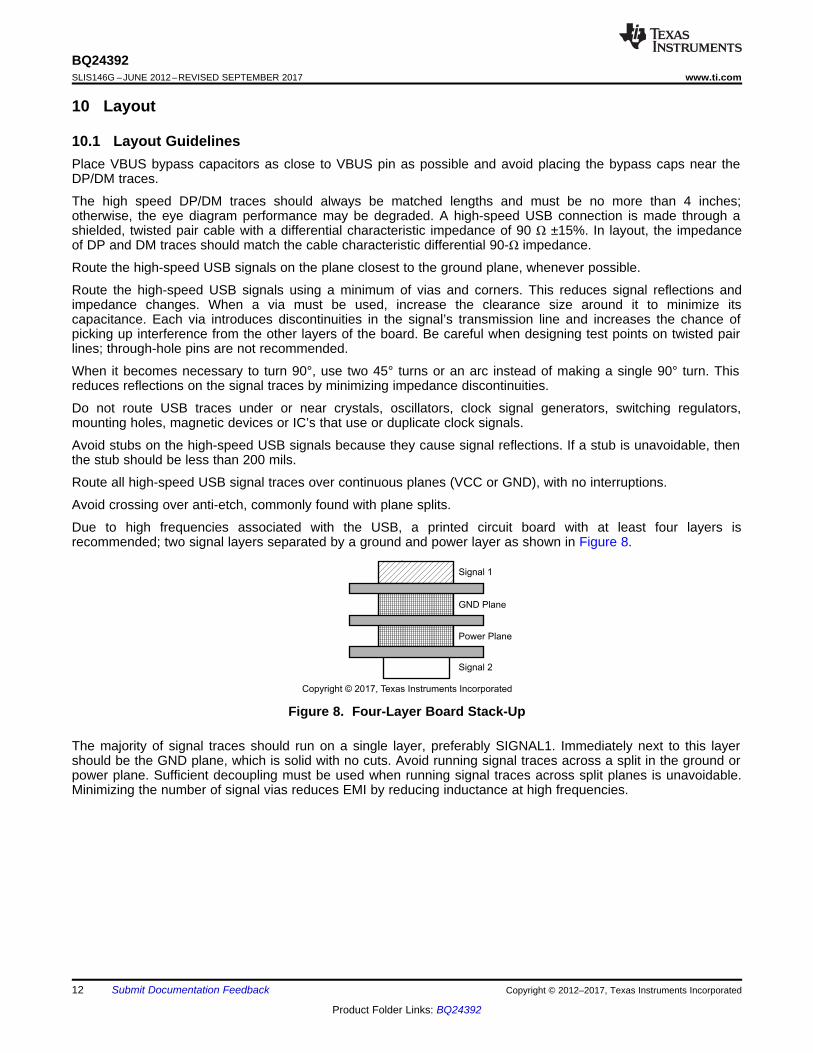
Due to high frequencies associated with the USB, a printed circuit board with at least four layers isrecommended; two signal layers separated by a ground and power layer as shown in Figure 8.
Figure 8. Four-Layer Board Stack-Up
The majority of signal traces should run on a single layer, preferably SIGNAL1. Immediately next to this layershould be the GND plane, which is solid with no cuts. Avoid running signal traces across a split in the ground orpower plane. Sufficient decoupling must be used when running signal traces across split planes is unavoidable.Minimizing the number of signal vias reduces EMI by reducing inductance at high frequencies.
11.1 Receiving Notification of Documentation UpdatesTo receive notification of documentation updates, navigate to the device product folder on ti.com. In the upperright corner, click on Alert me to register and receive a weekly digest of any product information that haschanged. For change details, review the revision history included in any revised document.
11.2 Community ResourcesThe following links connect to TI community resources. Linked contents are provided "AS IS" by the respectivecontributors. They do not constitute TI specifications and do not necessarily reflect TI's views; see TI's Terms ofUse.
TI E2E™ Online Community TI's Engineer-to-Engineer (E2E) Community. Created to foster collaborationamong engineers. At e2e.ti.com, you can ask questions, share knowledge, explore ideas and helpsolve problems with fellow engineers.
Design Support TI's Design Support Quickly find helpful E2E forums along with design support tools andcontact information for technical support.
11.3 TrademarksE2E is a trademark of Texas Instruments.Apple is a trademark of Apple.TomTom is a trademark of TomTom International.All other trademarks are the property of their respective owners.
11.4 Electrostatic Discharge CautionThese devices have limited built-in ESD protection. The leads should be shorted together or the device placed in conductive foamduring storage or handling to prevent electrostatic damage to the MOS gates.
12 Mechanical, Packaging, and Orderable InformationThe following pages include mechanical, packaging, and orderable information. This information is the mostcurrent data available for the designated devices. This data is subject to change without notice and revision ofthis document. For browser-based versions of this data sheet, refer to the left-hand navigation.
BQ24392RSER ACTIVE UQFN RSE 10 3000 Green (RoHS& no Sb/Br)
CU NIPDAUAG Level-1-260C-UNLIM -40 to 85 APH
(1) The marketing status values are defined as follows:ACTIVE: Product device recommended for new designs.LIFEBUY: TI has announced that the device will be discontinued, and a lifetime-buy period is in effect.NRND: Not recommended for new designs. Device is in production to support existing customers, but TI does not recommend using this part in a new design.PREVIEW: Device has been announced but is not in production. Samples may or may not be available.OBSOLETE: TI has discontinued the production of the device.
(2) RoHS: TI defines "RoHS" to mean semiconductor products that are compliant with the current EU RoHS requirements for all 10 RoHS substances, including the requirement that RoHS substancedo not exceed 0.1% by weight in homogeneous materials. Where designed to be soldered at high temperatures, "RoHS" products are suitable for use in specified lead-free processes. TI mayreference these types of products as "Pb-Free".RoHS Exempt: TI defines "RoHS Exempt" to mean products that contain lead but are compliant with EU RoHS pursuant to a specific EU RoHS exemption.Green: TI defines "Green" to mean the content of Chlorine (Cl) and Bromine (Br) based flame retardants meet JS709B low halogen requirements of <=1000ppm threshold. Antimony trioxide basedflame retardants must also meet the <=1000ppm threshold requirement.
(3) MSL, Peak Temp. - The Moisture Sensitivity Level rating according to the JEDEC industry standard classifications, and peak solder temperature.
(4) There may be additional marking, which relates to the logo, the lot trace code information, or the environmental category on the device.
(5) Multiple Device Markings will be inside parentheses. Only one Device Marking contained in parentheses and separated by a "~" will appear on a device. If a line is indented then it is a continuationof the previous line and the two combined represent the entire Device Marking for that device.
(6) Lead/Ball Finish - Orderable Devices may have multiple material finish options. Finish options are separated by a vertical ruled line. Lead/Ball Finish values may wrap to two lines if the finishvalue exceeds the maximum column width.
Important Information and Disclaimer:The information provided on this page represents TI's knowledge and belief as of the date that it is provided. TI bases its knowledge and belief on informationprovided by third parties, and makes no representation or warranty as to the accuracy of such information. Efforts are underway to better integrate information from third parties. TI has taken andcontinues to take reasonable steps to provide representative and accurate information but may not have conducted destructive testing or chemical analysis on incoming materials and chemicals.TI and TI suppliers consider certain information to be proprietary, and thus CAS numbers and other limited information may not be available for release.
In no event shall TI's liability arising out of such information exceed the total purchase price of the TI part(s) at issue in this document sold by TI to Customer on an annual basis.
Texas Instruments Incorporated (TI) reserves the right to make corrections, enhancements, improvements and other changes to itssemiconductor products and services per JESD46, latest issue, and to discontinue any product or service per JESD48, latest issue. Buyersshould obtain the latest relevant information before placing orders and should verify that such information is current and complete.TI’s published terms of sale for semiconductor products (http://www.ti.com/sc/docs/stdterms.htm) apply to the sale of packaged integratedcircuit products that TI has qualified and released to market. Additional terms may apply to the use or sale of other types of TI products andservices.Reproduction of significant portions of TI information in TI data sheets is permissible only if reproduction is without alteration and isaccompanied by all associated warranties, conditions, limitations, and notices. TI is not responsible or liable for such reproduceddocumentation. Information of third parties may be subject to additional restrictions. Resale of TI products or services with statementsdifferent from or beyond the parameters stated by TI for that product or service voids all express and any implied warranties for theassociated TI product or service and is an unfair and deceptive business practice. TI is not responsible or liable for any such statements.Buyers and others who are developing systems that incorporate TI products (collectively, “Designers”) understand and agree that Designersremain responsible for using their independent analysis, evaluation and judgment in designing their applications and that Designers havefull and exclusive responsibility to assure the safety of Designers' applications and compliance of their applications (and of all TI productsused in or for Designers’ applications) with all applicable regulations, laws and other applicable requirements. Designer represents that, withrespect to their applications, Designer has all the necessary expertise to create and implement safeguards that (1) anticipate dangerousconsequences of failures, (2) monitor failures and their consequences, and (3) lessen the likelihood of failures that might cause harm andtake appropriate actions. Designer agrees that prior to using or distributing any applications that include TI products, Designer willthoroughly test such applications and the functionality of such TI products as used in such applications.TI’s provision of technical, application or other design advice, quality characterization, reliability data or other services or information,including, but not limited to, reference designs and materials relating to evaluation modules, (collectively, “TI Resources”) are intended toassist designers who are developing applications that incorporate TI products; by downloading, accessing or using TI Resources in anyway, Designer (individually or, if Designer is acting on behalf of a company, Designer’s company) agrees to use any particular TI Resourcesolely for this purpose and subject to the terms of this Notice.TI’s provision of TI Resources does not expand or otherwise alter TI’s applicable published warranties or warranty disclaimers for TIproducts, and no additional obligations or liabilities arise from TI providing such TI Resources. TI reserves the right to make corrections,enhancements, improvements and other changes to its TI Resources. TI has not conducted any testing other than that specificallydescribed in the published documentation for a particular TI Resource.Designer is authorized to use, copy and modify any individual TI Resource only in connection with the development of applications thatinclude the TI product(s) identified in such TI Resource. NO OTHER LICENSE, EXPRESS OR IMPLIED, BY ESTOPPEL OR OTHERWISETO ANY OTHER TI INTELLECTUAL PROPERTY RIGHT, AND NO LICENSE TO ANY TECHNOLOGY OR INTELLECTUAL PROPERTYRIGHT OF TI OR ANY THIRD PARTY IS GRANTED HEREIN, including but not limited to any patent right, copyright, mask work right, orother intellectual property right relating to any combination, machine, or process in which TI products or services are used. Informationregarding or referencing third-party products or services does not constitute a license to use such products or services, or a warranty orendorsement thereof. Use of TI Resources may require a license from a third party under the patents or other intellectual property of thethird party, or a license from TI under the patents or other intellectual property of TI.TI RESOURCES ARE PROVIDED “AS IS” AND WITH ALL FAULTS. TI DISCLAIMS ALL OTHER WARRANTIES ORREPRESENTATIONS, EXPRESS OR IMPLIED, REGARDING RESOURCES OR USE THEREOF, INCLUDING BUT NOT LIMITED TOACCURACY OR COMPLETENESS, TITLE, ANY EPIDEMIC FAILURE WARRANTY AND ANY IMPLIED WARRANTIES OFMERCHANTABILITY, FITNESS FOR A PARTICULAR PURPOSE, AND NON-INFRINGEMENT OF ANY THIRD PARTY INTELLECTUALPROPERTY RIGHTS. TI SHALL NOT BE LIABLE FOR AND SHALL NOT DEFEND OR INDEMNIFY DESIGNER AGAINST ANY CLAIM,INCLUDING BUT NOT LIMITED TO ANY INFRINGEMENT CLAIM THAT RELATES TO OR IS BASED ON ANY COMBINATION OFPRODUCTS EVEN IF DESCRIBED IN TI RESOURCES OR OTHERWISE. IN NO EVENT SHALL TI BE LIABLE FOR ANY ACTUAL,DIRECT, SPECIAL, COLLATERAL, INDIRECT, PUNITIVE, INCIDENTAL, CONSEQUENTIAL OR EXEMPLARY DAMAGES INCONNECTION WITH OR ARISING OUT OF TI RESOURCES OR USE THEREOF, AND REGARDLESS OF WHETHER TI HAS BEENADVISED OF THE POSSIBILITY OF SUCH DAMAGES.Unless TI has explicitly designated an individual product as meeting the requirements of a particular industry standard (e.g., ISO/TS 16949and ISO 26262), TI is not responsible for any failure to meet such industry standard requirements.Where TI specifically promotes products as facilitating functional safety or as compliant with industry functional safety standards, suchproducts are intended to help enable customers to design and create their own applications that meet applicable functional safety standardsand requirements. Using products in an application does not by itself establish any safety features in the application. Designers mustensure compliance with safety-related requirements and standards applicable to their applications. Designer may not use any TI products inlife-critical medical equipment unless authorized officers of the parties have executed a special contract specifically governing such use.Life-critical medical equipment is medical equipment where failure of such equipment would cause serious bodily injury or death (e.g., lifesupport, pacemakers, defibrillators, heart pumps, neurostimulators, and implantables). Such equipment includes, without limitation, allmedical devices identified by the U.S. Food and Drug Administration as Class III devices and equivalent classifications outside the U.S.TI may expressly designate certain products as completing a particular qualification (e.g., Q100, Military Grade, or Enhanced Product).Designers agree that it has the necessary expertise to select the product with the appropriate qualification designation for their applicationsand that proper product selection is at Designers’ own risk. Designers are solely responsible for compliance with all legal and regulatoryrequirements in connection with such selection.Designer will fully indemnify TI and its representatives against any damages, costs, losses, and/or liabilities arising out of Designer’s non-compliance with the terms and provisions of this Notice.