190


BROADBAND OPTO-ELECTRICAL RECEIVERSIN STANDARD CMOS
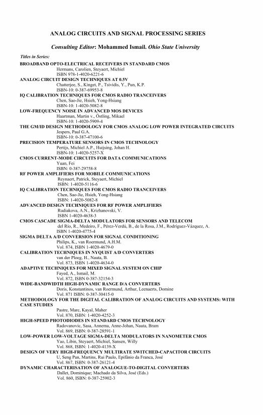
ANALOG CIRCUITS AND SIGNAL PROCESSING SERIES
Consulting Editor: Mohammed Ismail. Ohio State University Titles in Series:
ANALOG CIRCUIT DESIGN TECHNIQUES AT 0.5V Chatterjee, S., Kinget, P., Tsividis, Y., Pun, K.P. ISBN-10: 0-387-69953-8
IQ CALIBRATION TECHNIQUES FOR CMOS RADIO TRANCEIVERS Chen, Sao-Jie, Hsieh, Yong-Hsiang ISBN-10: 1-4020-5082-8
LOW-FREQUENCY NOISE IN ADVANCED MOS DEVICES Haartman, Martin v., Östling, Mikael ISBN-10: 1-4020-5909-4
THE GM/ID DESIGN METHODOLOGY FOR CMOS ANALOG LOW POWER INTEGRATED CIRCUITS Jespers, Paul G.A. ISBN-10: 0-387-47100-6
PRECISION TEMPERATURE SENSORS IN CMOS TECHNOLOGY Pertijs, Michiel A.P., Huijsing, Johan H. ISBN-10: 1-4020-5257-X
CMOS CURRENT-MODE CIRCUITS FOR DATA COMMUNICATIONS Yuan, Fei ISBN: 0-387-29758-8
RF POWER AMPLIFIERS FOR MOBILE COMMUNICATIONS Reynaert, Patrick, Steyaert, Michiel ISBN: 1-4020-5116-6 IQ CALIBRATION TECHNIQUES FOR CMOS RADIO TRANCEIVERS Chen, Sao-Jie, Hsieh, Yong-Hsiang ISBN: 1-4020-5082-8 ADVANCED DESIGN TECHNIQUES FOR RF POWER AMPLIFIERS Rudiakova, A.N., Krizhanovski, V. ISBN 1-4020-4638-3 CMOS CASCADE SIGMA-DELTA MODULATORS FOR SENSORS AND TELECOM
del Río, R., Medeiro, F., Pérez-Verdú, B., de la Rosa, J.M., Rodríguez-Vázquez, A. ISBN 1-4020-4775-4
Philips, K., van Roermund, A.H.M. Vol. 874, ISBN 1-4020-4679-0
CALIBRATION TECHNIQUES IN NYQUIST A/D CONVERTERS van der Ploeg, H., Nauta, B. Vol. 873, ISBN 1-4020-4634-0
ADAPTIVE TECHNIQUES FOR MIXED SIGNAL SYSTEM ON CHIP Fayed, A., Ismail, M. Vol. 872, ISBN 0-387-32154-3
WIDE-BANDWIDTH HIGH-DYNAMIC RANGE D/A CONVERTERS Doris, Konstantinos, van Roermund, Arthur, Leenaerts, Domine Vol. 871 ISBN: 0-387-30415-0
METHODOLOGY FOR THE DIGITAL CALIBRATION OF ANALOG CIRCUITS AND SYSTEMS: WITH CASE STUDIES
Pastre, Marc, Kayal, Maher Vol. 870, ISBN: 1-4020-4252-3
HIGH-SPEED PHOTODIODES IN STANDARD CMOS TECHNOLOGY Radovanovic, Sasa, Annema, Anne-Johan, Nauta, Bram Vol. 869, ISBN: 0-387-28591-1
LOW-POWER LOW-VOLTAGE SIGMA-DELTA MODULATORS IN NANOMETER CMOS Yao, Libin, Steyaert, Michiel, Sansen, Willy Vol. 868, ISBN: 1-4020-4139-X
DESIGN OF VERY HIGH-FREQUENCY MULTIRATE SWITCHED-CAPACITOR CIRCUITS U, Seng Pan, Martins, Rui Paulo, Epifânio da Franca, José Vol. 867, ISBN: 0-387-26121-4
DYNAMIC CHARACTERISATION OF ANALOGUE-TO-DIGITAL CONVERTERS Dallet, Dominique; Machado da Silva, José (Eds.) Vol. 860, ISBN: 0-387-25902-3
SIGMA DELTA A/D CONVERSION FOR SIGNAL CONDITIONING
BROADBAND OPTO-ELECTRICAL RECEIVERS IN STANDARD CMOSHermans, Carolien, Steyaert, MichielISBN 978-1-4020-6221-6

Broadband Opto-Electrical Receiversin Standard CMOS
By
CAROLIEN HERMANSKU Leuven, Belgium
and
MICHIEL STEYAERTKU Leuven, Belgium

A C.I.P. Catalogue record for this book is available from the Library of Congress.
ISBN 978-1-4020-6221-6 (HB)ISBN 978-1-4020-6222-3 (e-book)
Published by Springer,P.O. Box 17, 3300 AA Dordrecht, The Netherlands.
www.springer.com
Printed on acid-free paper
All Rights Reservedc© 2007 Springer
No part of this work may be reproduced, stored in a retrieval system, or transmittedin any form or by any means, electronic, mechanical, photocopying, microfilming,recording or otherwise, without written permission from the Publisher, with the exceptionof any material supplied specifically for the purpose of being entered and executed on acomputer system, for exclusive use by the purchaser of the work.

Preface
The gradual recovery of the optical industry since 2004 has enabled new de-velopments in the communication, consumer and entertainment markets. Lotsof new applications are emerging where high volumes and low cost aspects arecrucial. To meet these demands, silicon microphotonics aims for the manufac-turing of opto-electrical components in the same platform that has enabledMoore’s Law: single-crystal silicon.
The presented work fits in this quest for integrated opto-electrical solu-tions, and focuses on the receiver front-end. To further reduce the cost, thecheapest technology is selected: standard CMOS, without any optical tricks orflavors. Despite the inherent lower optical performance of a mainstream CMOSprocess, it is shown in theory and practice that light detection is feasible withCMOS diodes. Furthermore, speed enhancement techniques are presented toextend the speed performance above 1 Gbit/s.
The three receiver blocks examined in this work are the photodiode(PD), the transimpedance amplifier (TIA) and the limiting amplifier (LA).First, to thoroughly understand the light detection mechanisms in silicon,the basic semiconductor one-dimensional equations are studied. Next, a two-dimensional model is developed to compare the performance of different typesof photodiodes implemented in successive technology generations and for threeinput wavelengths. Analytical design equations are derived to guide the designof the amplifying circuits. For the TIA, the focus lies on the sensitivity-speedtrade-off. For the LA, a high gain-bandwidth is pursued.
Theory is put into practice through several CMOS implementations. Afirst 0.18 µm chip compares different photodiode topologies. The differentialdiode with TIA has the best high-speed performance and achieves a BER of3 · 10−10 when a 500 Mbit/s optical signal of −8 dBm is applied. Next, dif-ferent photodiode topologies manufactured in a 90 nm CMOS technology arecompared. The best results are obtained with the p+ n-well diode with guard.This diode with TIA can handle data with bitrates up to 500 Mbit/s and anoptical power of −8 dBm, showing a BER of 10−9. A third chip containsa LA implemented in 0.18 µm CMOS and based on a cascade of Cherry-
v

vi Preface
Hooper stages. Eye diagrams at 3.5 Gbit/s illustrate the applied broadbandtechniques.
Finally, all knowledge is gathered in the design of a monolithic opticalreceiver front-end in 0.18 µm CMOS. This chip contains a differential CMOSphotodiode, a differential two-stage TIA with cross-coupled feed-back and ahigh-gain broadband LA. The speed performance of the photodiode is fur-ther enhanced by an analog equalizer. The TIA achieves a transimpedance-bandwidth product of 19 THzΩ. The LA features a gain-bandwidth productof 397 GHz. At 6 Gbit/s, the LA with output buffer has a BER of 10−12 when8 mVpp is applied at the input. The complete receiver is characterized by aBER smaller than 10−12 for a −6 dBm optical input signal with a bitrate of1.7 Gbit/s. This receiver competes with present state-of-the-art and is, to theauthor’s knowledge, the first CMOS Gbit/s opto-electrical receiver integratingPD, TIA and LA on the same die.
Heverlee, Carolien HermansMarch 2007 Michiel Steyaert

List of Abbreviations and Symbols
Abbreviations
ac Alternating CurrentAGC Automatic Gain ControlBER Bit Error RateBiCMOS Bipolar Complementary Metal Oxide SemiconductorCD Compact DiscCDR Clock and Data RecoveryCG Common GateCMOS Complementary Metal Oxide SemiconductorCMU Clock Multiplication UnitCSD Capacitive Source DegenerationDC Direct CurrentDG Diffraction GratingDMUX DemultiplexerDSL Digital Subscriber LoopDVI Digital Video InterfaceDVD Digital Versatile DiscDWDM Dense Wavelength-Division MultiplexingECL Emitter Coupled LogicFTTH Fiber-To-The-HomeGaAs Gallium ArsenideGaN Gallium NitrideGB GigabyteGe GermaniumHD-DVD High Density Digital Versatile DiscIC Integrated CircuitIn0.53Ga0.47As Indium Gallium ArsenideInP Indium PhosphideISI Intersymbol InterferenceISSCC International Solid-State Circuits Conference
vii

viii List of Abbreviations and Symbols
LA Limiting AmplifierLAN Local Area NetworkLD Laser DiodeLED Light Emitting DiodeMAN Metro(politan) Area NetworkMOS Metal Oxide SemiconductorMOST Media Oriented System TransportMUX MultiplexernMOS n-channel MOS transistorNA Numerical ApertureNIC Negative Impedance ConverterNRZ Non-Return-to-ZeropMOS p-channel MOS transistorprbs Pseudorandom Bit SequencePA Post-AmplifierParBERT Parallel Bit Error Ratio TesterPBS Polarization Beam SplitterPCS Polymer-Clad SilicaP.M. Phase MarginPMMA Polymethyl MethacrylateP.O. Percent OvershootPOF Plastic Optical FiberPON Passive Optical NetworksOEIC Opto-electronic Integrated CircuitPOF Plastic Optical FiberQWP Quarter-Wave PlateRGC Regulated CascodeRZ Return-to-ZeroSAN Storage Area NetworkSDH Synchronous Digital HierarchySi SiliconSiO2 Silicon dioxideSML-detector Spatially Modulated Light detectorSNR Signal to Noise RatioSOI Silicon on InsulatorSONET Synchronous Optical NetworkTAS Transadmittance StageTIA Transimpedance AmplifierTIS Transimpedance StageUI Unite IntervalVA Voltage AmplifierVCSEL Vertical-Cavity Surface-Emitting laserVUC Voltage-Up-ConverterWAN Wide Area NetworksWDM Wavelength-Division Multiplexing

List of Abbreviations and Symbols ix
Symbols
A voltage gainA0 DC voltage gainA1st differential gain of a single stage of a post-amplifierACH differential gain of a Cherry-Hooper stageACSD differential gain of a voltage amplifier with
capacitive source degenerationAdiff differential gainAos gain of an offset compensation amplifierAPA gain of a post-amplifierAPA,0 mid-band gain of a post-amplifierBWn noise bandwidthBWPA 3-dB bandwidth of a post-amplifierBWTIA 3-dB bandwidth of a TIABWV A 3-dB bandwidth of a voltage amplifierc speed of light in vacuumCdio diode junction capacitanceCds drain-source capacitanceCgs gate-source capacitanceCin input capacitanceCinT total input capacitanceCnext input capacitance of the next stageCout output capacitanceCoutT total output capacitanceCox oxide capacitancedi2dio diode shot noisedi2Mα thermal channel noise of transistor Mα
di2n,TIA power spectral density of the TIA input-referrednoise current
di2Rα thermal current noise of transistor Rα
dv2n,TIA power spectral density of the TIA output noise voltage
Dn electron diffusion constantDp hole diffusion constantEg bandgap energyEp photon energyf0dB,GH unity-gain frequency of the loop gainf3dB 3-dB bandwidthf3dB,1st 3-dB bandwidth of a single stage of a post-amplifierf3dB,PA 3-dB bandwidth of a post-amplifierfd,GH dominant pole of the loop gainfLF low-frequency cut-off

x List of Abbreviations and Symbols
fnd,GH non-dominant pole of the loop gainfnd,TIA non-dominant pole of TIAfT unity current gain frequencyFBW factor defined by the ratio of BWV A and BWTIA
gds transistor output conductancegm transistor transconductanceG light generation termGeq transfer function of the equalizerGm,CSD effective transconductance of an amplifier stage with
capacitive source degenerationGTIA TIA open-loop gainGBW gain-bandwidth productGHTIA TIA loop gainh Planck’s constantiin small-signal input currentin,rms equivalent input-referred rms noisein,OR total integrated input-referred optical receiver
current noisein,TIA total integrated input-referred TIA current noiseisenspp electrical receiver sensitivity
Idio diode currentIds drain-source currentJdrift drift current densityJdiffn electron diffusion current densityJdiffp hole diffusion current densityK ′
n transconductance parameter for an nMOS transistorK ′
p transconductance parameter for a pMOS transistorL transistor lengthLMCH loop gain of the feedback loop in the modified
Cherry-Hooper stageLb depth in the substrate where n = n0
Lnw depth of the n-well, upper edge of space charge regionLscr lower edge of the space charge regionLsd depth of the source/drain region, upper edge of the space
charge regionMi Miller factorn electron concentrationn(t) noise voltagen0 initial electron concentrationNA acceptor concentration in p-substrateND donor concentration in n-wellNf number of fingers in a photodiode topologyNs number of squares in a photodiode topologyp hole concentrationp0 initial hole concentration

List of Abbreviations and Symbols xi
P sensav optical receiver sensitivity
Pdiss power dissipationPn probability density function for noisePopt (average) optical powerPx probability density function for the wanted signalq elementary chargeQ(x) Q functionR responsivity of a photodiodeRb bitrateRdark responsivity of the dark junctionsRf feedback resistanceRlight responsivity of the illuminated junctionsRout output resistanceSout power spectral density of the output signalt timeTb bit periodvn,LA total integrated input-referred limiting amplifier
voltage noisevn,rms rms noise voltagevout small-signal output voltagevpp peak-to-peak value of the received signalVbi built-in voltageVds drain-source voltageVgs gate-source voltageVDSAT saturation voltage of a MOS transistorVR reverse voltageVT threshold voltage of a transistorVTH threshold voltage of the decision circuitV0 logic zero levelV1 logic one levelW transistor widthx depthx(t) received signal voltageXN ratio of Cgs to Cdio
ZBW transimpedance-bandwidth productZin,0 DC input impedanceZNIC impedance of a negative impedance converterZTIA TIA transimpedance gainZTIA,0 TIA DC transimpedance gainα absorption coefficient of light (in Silicon)αgd ratio between Cgd and Cgs
γ excess noise factorεSi Silicon permittivityζ damping ratio of a second-order systemη quantum efficiency of a photodiode
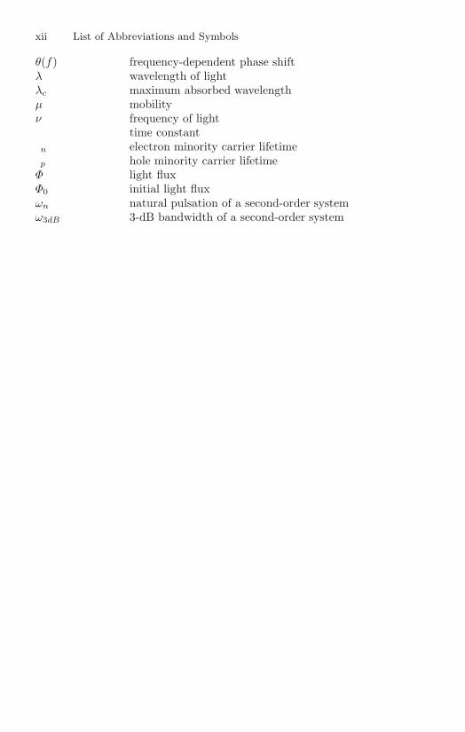
xii List of Abbreviations and Symbols
θ(f) frequency-dependent phase shiftλ wavelength of lightλc maximum absorbed wavelengthμ mobilityν frequency of lightτ time constantτn electron minority carrier lifetimeτp hole minority carrier lifetimeΦ light fluxΦ0 initial light fluxωn natural pulsation of a second-order systemω3dB 3-dB bandwidth of a second-order system

Contents
Preface . . . . . . . . . . . . . . . . . . . . . . . . . . . . . . . . . . . . . . . . . . . . . . . . . . . . . . . . v
List of Abbreviations and Symbols . . . . . . . . . . . . . . . . . . . . . . . . . . . . . vii
1 Introduction . . . . . . . . . . . . . . . . . . . . . . . . . . . . . . . . . . . . . . . . . . . . . . . 11.1 A History of Optical Communication . . . . . . . . . . . . . . . . . . . . . . 11.2 Emerging Applications . . . . . . . . . . . . . . . . . . . . . . . . . . . . . . . . . . . 41.3 Silicon Opto-Electronics . . . . . . . . . . . . . . . . . . . . . . . . . . . . . . . . . . 71.4 Outline of the Work . . . . . . . . . . . . . . . . . . . . . . . . . . . . . . . . . . . . . 9
2 Optical Receiver Fundamentals . . . . . . . . . . . . . . . . . . . . . . . . . . . . 132.1 Introduction . . . . . . . . . . . . . . . . . . . . . . . . . . . . . . . . . . . . . . . . . . . . 132.2 The Optical Receiver Front-End . . . . . . . . . . . . . . . . . . . . . . . . . . . 13
2.2.1 A Transceiver for Optical Communication Systems . . . . 132.2.2 A Pickup Unit for Optical Storage Systems . . . . . . . . . . . 15
2.3 Binary Data Formats . . . . . . . . . . . . . . . . . . . . . . . . . . . . . . . . . . . . 172.4 Bit Error Rate and Sensitivity . . . . . . . . . . . . . . . . . . . . . . . . . . . . 20
2.4.1 Bit Error Rate . . . . . . . . . . . . . . . . . . . . . . . . . . . . . . . . . . . . 202.4.2 Sensitivity . . . . . . . . . . . . . . . . . . . . . . . . . . . . . . . . . . . . . . . . 22
2.5 Intersymbol Interference . . . . . . . . . . . . . . . . . . . . . . . . . . . . . . . . . . 232.5.1 Low-Pass Filtering . . . . . . . . . . . . . . . . . . . . . . . . . . . . . . . . . 232.5.2 High-Pass Filtering . . . . . . . . . . . . . . . . . . . . . . . . . . . . . . . . 24
2.6 Jitter . . . . . . . . . . . . . . . . . . . . . . . . . . . . . . . . . . . . . . . . . . . . . . . . . . 252.7 Conclusions . . . . . . . . . . . . . . . . . . . . . . . . . . . . . . . . . . . . . . . . . . . . . 26
3 Standard CMOS Photodiodes . . . . . . . . . . . . . . . . . . . . . . . . . . . . . 273.1 Introduction . . . . . . . . . . . . . . . . . . . . . . . . . . . . . . . . . . . . . . . . . . . . 273.2 Basic Concepts . . . . . . . . . . . . . . . . . . . . . . . . . . . . . . . . . . . . . . . . . . 27
3.2.1 Principles of Light Detection . . . . . . . . . . . . . . . . . . . . . . . . 283.2.2 The Use of Standard CMOS . . . . . . . . . . . . . . . . . . . . . . . . 31
3.3 Overview of Published Integrated Photodiodes . . . . . . . . . . . . . . 32
xiii

xiv Contents
3.3.1 BiCMOS Implementations . . . . . . . . . . . . . . . . . . . . . . . . . . 323.3.2 SOI Implementations . . . . . . . . . . . . . . . . . . . . . . . . . . . . . . 343.3.3 CMOS Implementations . . . . . . . . . . . . . . . . . . . . . . . . . . . . 353.3.4 Conclusions . . . . . . . . . . . . . . . . . . . . . . . . . . . . . . . . . . . . . . . 36
3.4 One-Dimensional Model . . . . . . . . . . . . . . . . . . . . . . . . . . . . . . . . . . 373.4.1 N-Well P-Substrate Junction . . . . . . . . . . . . . . . . . . . . . . . . 373.4.2 P+ N-Well Junction with Guard . . . . . . . . . . . . . . . . . . . . 43
3.5 Two-Dimensional Model . . . . . . . . . . . . . . . . . . . . . . . . . . . . . . . . . . 463.5.1 Classical N-Well Diode . . . . . . . . . . . . . . . . . . . . . . . . . . . . . 463.5.2 P+ N-Well Diode with Guard . . . . . . . . . . . . . . . . . . . . . . . 493.5.3 Differential N-Well Diode . . . . . . . . . . . . . . . . . . . . . . . . . . . 513.5.4 Influence of Wavelength . . . . . . . . . . . . . . . . . . . . . . . . . . . . 523.5.5 Influence of Technology Scaling . . . . . . . . . . . . . . . . . . . . . 56
3.6 Conclusions . . . . . . . . . . . . . . . . . . . . . . . . . . . . . . . . . . . . . . . . . . . . . 58
4 Transimpedance Amplifier Design . . . . . . . . . . . . . . . . . . . . . . . . . 614.1 Introduction . . . . . . . . . . . . . . . . . . . . . . . . . . . . . . . . . . . . . . . . . . . . 614.2 Performance Requirements . . . . . . . . . . . . . . . . . . . . . . . . . . . . . . . 614.3 Design of the Shunt-Shunt Feedback TIA . . . . . . . . . . . . . . . . . . . 63
4.3.1 Transimpedance Gain and Bandwidth . . . . . . . . . . . . . . . . 644.3.2 Open-Loop Gain and Loop Gain . . . . . . . . . . . . . . . . . . . . 684.3.3 Noise . . . . . . . . . . . . . . . . . . . . . . . . . . . . . . . . . . . . . . . . . . . . 70
4.4 Literature Examples . . . . . . . . . . . . . . . . . . . . . . . . . . . . . . . . . . . . . 764.4.1 Common Source TIA . . . . . . . . . . . . . . . . . . . . . . . . . . . . . . 774.4.2 Regulated Cascode TIA . . . . . . . . . . . . . . . . . . . . . . . . . . . . 784.4.3 The Latest Trends at ISSCC . . . . . . . . . . . . . . . . . . . . . . . . 80
4.5 Case Studies . . . . . . . . . . . . . . . . . . . . . . . . . . . . . . . . . . . . . . . . . . . . 814.5.1 An Inverter-Based TIA for Test Photodiodes
in 0.18 µm CMOS. . . . . . . . . . . . . . . . . . . . . . . . . . . . . . . . . 824.5.2 An Inverter-Based TIA for Test Photodiodes
in 90 nm CMOS. . . . . . . . . . . . . . . . . . . . . . . . . . . . . . . . . . . 934.5.3 A Differential Bandwidth-Optimized TIA in 0.18 µm
CMOS . . . . . . . . . . . . . . . . . . . . . . . . . . . . . . . . . . . . . . . . . . . 974.6 Conclusions . . . . . . . . . . . . . . . . . . . . . . . . . . . . . . . . . . . . . . . . . . . . . 103
5 Post-Amplifier Design . . . . . . . . . . . . . . . . . . . . . . . . . . . . . . . . . . . . . 1075.1 Introduction . . . . . . . . . . . . . . . . . . . . . . . . . . . . . . . . . . . . . . . . . . . . 1075.2 Performance Requirements . . . . . . . . . . . . . . . . . . . . . . . . . . . . . . . 1085.3 Literature Examples . . . . . . . . . . . . . . . . . . . . . . . . . . . . . . . . . . . . . 1105.4 Design of a Fully Differential Broadband LA . . . . . . . . . . . . . . . . 113
5.4.1 Cascaded Gain Stages . . . . . . . . . . . . . . . . . . . . . . . . . . . . . . 1145.4.2 Broadband Cherry-Hooper Stage . . . . . . . . . . . . . . . . . . . . 1165.4.3 Broadband Stage with Capacitive Source Degeneration . 1205.4.4 Offset Compensation . . . . . . . . . . . . . . . . . . . . . . . . . . . . . . . 122
5.5 Case Studies . . . . . . . . . . . . . . . . . . . . . . . . . . . . . . . . . . . . . . . . . . . . 124

Contents xv
5.5.1 A Four-Stage LA in 0.18 µm CMOS . . . . . . . . . . . . . . . . . 1245.5.2 A Five-Stage LA with Offset Compensation
in 0.18 µm CMOS. . . . . . . . . . . . . . . . . . . . . . . . . . . . . . . . . 1265.6 Conclusions . . . . . . . . . . . . . . . . . . . . . . . . . . . . . . . . . . . . . . . . . . . . . 129
6 CMOS Realizations . . . . . . . . . . . . . . . . . . . . . . . . . . . . . . . . . . . . . . . . 1336.1 Introduction . . . . . . . . . . . . . . . . . . . . . . . . . . . . . . . . . . . . . . . . . . . . 1336.2 Test Photodiodes with TIA in 0.18 µm CMOS . . . . . . . . . . . . . 135
6.2.1 Circuit Description . . . . . . . . . . . . . . . . . . . . . . . . . . . . . . . . 1356.2.2 Measurements . . . . . . . . . . . . . . . . . . . . . . . . . . . . . . . . . . . . 138
6.3 Test Photodiodes with TIA in 90 nm CMOS . . . . . . . . . . . . . . . . 1426.3.1 Circuit Description . . . . . . . . . . . . . . . . . . . . . . . . . . . . . . . . 1436.3.2 Measurements . . . . . . . . . . . . . . . . . . . . . . . . . . . . . . . . . . . . 144
6.4 A 3.5 Gbit/s LA in 0.18 µm CMOS . . . . . . . . . . . . . . . . . . . . . . . 1466.4.1 Circuit Description . . . . . . . . . . . . . . . . . . . . . . . . . . . . . . . . 1476.4.2 Measurements . . . . . . . . . . . . . . . . . . . . . . . . . . . . . . . . . . . . 149
6.5 A Gbit/s Monolithic Optical Receiver Front-Endin 0.18 µm CMOS . . . . . . . . . . . . . . . . . . . . . . . . . . . . . . . . . . . . . . 1526.5.1 Circuit Description . . . . . . . . . . . . . . . . . . . . . . . . . . . . . . . . 1526.5.2 Measurements . . . . . . . . . . . . . . . . . . . . . . . . . . . . . . . . . . . . 157
6.6 Conclusions . . . . . . . . . . . . . . . . . . . . . . . . . . . . . . . . . . . . . . . . . . . . . 164
7 Conclusions . . . . . . . . . . . . . . . . . . . . . . . . . . . . . . . . . . . . . . . . . . . . . . . . 167
References . . . . . . . . . . . . . . . . . . . . . . . . . . . . . . . . . . . . . . . . . . . . . . . . . . . . . 171
Index . . . . . . . . . . . . . . . . . . . . . . . . . . . . . . . . . . . . . . . . . . . . . . . . . . . . . . . . . . 177

1
Introduction
1.1 A History of Optical Communication
Light as means of communication is not only used in our sophisticated,technology-driven modern era. Since earlier times, man has depended on lightto send messages, mostly in the form of fire. The Greek tragedian Aeschylusportrays in the ‘Oresteia’ trilogy (458 BC) how the news about the fall ofTroy was sent by fire signals via an unbroken line of beacon-fires from AsiaMinor to Mycenae. A few centuries later, the Greek historian Polybius writes‘The Histories’ or ‘The Rise of the Roman Empire’, covering the period of220 BC to 146 BC. In this work, he describes an arrangement by which thewhole Greek alphabet could be transmitted by fire signals using a two-digit,five level code. This communication link allowed the transmission of messagesnot previously agreed upon.
The first development of a useful optical telegraph dates from the timeof the French Revolution. As France was threatened by inner and outer op-ponents, a new communication system was necessary. The civilian ClaudeChappe, a former priest, invented a mechanical-optical telegraph. It consistedof a column with a movable crosswise beam. This beam also had two movablearms. Each arm had seven positions, and the crosswise beam had four more,permitting a 196-combination code. The arms were from 1 m to 10 m long,black, and counterweighted, moved by only two handles. Lamps mounted onthe arms proved unsatisfactory for night use. The equipment stood on rooftopsor towers, placed from 12 km to 25 km apart. Each tower had a telescopepointing both up and down the relay line. The first telegraph line of this sortwas put into operation in 1794. The telegraph line consisted of 22 stationsand linked Lille with the capital Paris, a distance of over 240 kilometers. Itonly took 2 to 6 minutes to transfer a message, riding couriers would haveneeded 30 hours. Other lines were built, including a line from Paris to Toulon.The system was widely copied by other European states, and was used byNapoleon to coordinate his empire and army. In the middle of the 19th cen-tury, the optical telegraph was replaced by the electrical telegraph, patented
1

2 1 Introduction
by Samual Morse in 1837. Major advantage of the latter system was a fastersignal transmission.
In 1880, Alexander Graham Bell invented the photophone. Bell consideredthis a greater discovery than his previous invention, the telephone. Bell’s pho-tophone worked by projecting voice through an instrument towards a mirror.Vibrations in the voice caused similar vibrations in the mirror. Bell directedsunlight into the mirror, which captured and projected the mirror’s vibra-tions. The receiver’s mirror received the light and caused a selenium crystalto vibrate, and the sound would come out on the other end. Although thephotophone was successful in allowing conversation over open space at a dis-tance up to 200 m, it had a few drawbacks: it did not work well at night, inthe rain, or if someone walked between the signal and the receiver. Eventually,Bell gave up on this idea.
These anecdotes illustrate that people always have tried to use light, evenin its most primitive form, to deliver some type of information between remotelocations. The most important drawback is the dependence on atmosphericconditions, that makes direct optical communication through the air unreli-able. The advent of the laser in the early 60’s was an important revolutionand boosted the development of optical communication systems. The solutionto the atmospheric disturbances was found to be the use of optical waveg-uides that forces the laser beam to follow a certain path. One of the pioneersin the field of fiber optics is the Dutch scientist Abraham van Heel. In thebeginning of the 50’s, he tried to solve the problem of light loss in fibers byusing a cladding material. All earlier fibers developed were bare and lackedany form of cladding, with total internal reflection occurring at a glass-air in-terface. The transparent cladding, with a lower refractive index than the glassor plastic fiber, protected the total reflection surface from contamination andgreatly reduced the crosstalk between fibers. By 1960, glass-clad fibers hadan attenuation of about 1000 dB/km, fine for medical imaging, but much toohigh for communication applications.
An important milestone in the history of fiber-optic communications is thepaper [Kao66], published in 1966 by Charles Kao and George Hockam. Theyshowed that optical fiber communication would be feasible if the transmis-sion loss could be reduced to less than 20 dB/km. Moreover, they proved thatthere was no fundamental mechanism that would prevent this loss from be-ing achieved. Only 4 years later, in 1970, Robert Maurer, Donald Keck andPeter Schultz of Corning Glass Corporation achieved this goal and manu-factured the first optical fiber with an attenuation less than 20 dB/km. By1980, the attenuation loss was reduced even further, and firms were experi-menting with putting cables under the sea. The first international underseafiber-optic link, which linked England with Belgium, was installed in 1986.By the end of 1988, the first transatlantic fiber-optic cable, connecting theUnited States with Europe, was a fact. The evolution of long-haul communi-cation systems in summarized in Table 1.1. Every generation is characterizedby a considerable increase in bitrate-distance product, the figure of merit com-
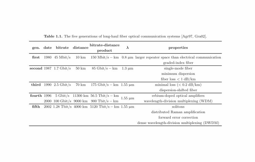
Table 1.1. The five generations of long-haul fiber optical communication systems [Agr97, Gra02].
gen. date bitrate distancebitrate-distance
λ propertiesproduct
first 1980 45 Mbit/s 10 km 150 Mbit/s − km 0.8 µm larger repeater space than electrical communication
graded-index fiber
second 1987 1.7 Gbit/s 50 km 85 Gbit/s − km 1.3 µm single-mode fiber
minimum dispersion
fiber loss < 1 dB/km
third 1990 2.5 Gbit/s 70 km 175 Gbit/s − km 1.55 µm minimal loss (< 0.2 dB/km)
dispersion-shifted fiber
fourth 1996 5 Gbit/s 11300 km 56.5 Tbit/s − km1.55 µm
erbium-doped optical amplifiers
2000 100 Gbit/s 9000 km 900 Tbit/s − km wavelength-division multiplexing (WDM)
fifth 2002 1.28 Tbit/s 4000 km 5120 Tbit/s − km 1.55 µm solitons
distributed Raman amplification
forward error correction
dense wavelength-division multiplexing (DWDM)

4 1 Introduction
monly used for optical communication systems. In the early generations, thiscapacity increase was mainly due to an improvement of the fiber properties(lower dispersion, minimal loss), combined with the development of lasersand detectors operating at longer wavelengths. During the fourth generation,the electrical repeater distance was drastically raised by using erbium-dopedamplifiers, spaced 60 km to 100 km apart, that regenerate the signal opti-cally. The bitrate on the other hand was increased by using the technique ofwavelength-division multiplexing (WDM). The era of terabit communicationsystems has truly arrived with the fifth generation. Todays’ commercial equip-ments are capable of sending 2.56 Tbit/s (64x40 Gbit/s channels) data overa distance of up to 1000 km, or 1.28 Tbit/s (128x10 Gbit/s channels) dataover a distance of up to 4000 km, without any electrical regeneration. Thekey technologies to realize this high capacity are solitons, distributed Ramanamplification, forward error correction and dense WDM [Gra02].
1.2 Emerging Applications
As revealed in the previous section, the historical popularity of optical fibercommunication is mainly due to the need of larger bitrate-distance productsin the field of long-haul communication systems. This section takes a look atsome other opto-electrical domains where interesting movements are going on.
Short-Distance Communication Networks
Optical fiber networks have many advantages over copper networks. Besidesthe high bitrate-distance product, exploited by long-haul communication net-works, optical fibers are insensitive to spurious noise signals and avoid elec-trical ground loops. However, the ultimate reason to replace copper wireswith optical fibers remains a purely economical one: a lower cost. Nowadays,bandwidth demands for short-distance communications are increasing expo-nentially. As a consequence, the critical point will be reached soon whereimproving the technology supporting these high-bandwidth applications overcopper wires will cost more than accomplishing the same speed over fiber.To make short-distance fiber communication affordable, the industry has de-veloped low-cost solutions like high-bandwidth multimode fibers and 850 nmtransceivers. Eventually, fiber optics will find its way in local area networks(LANs) and new systems like fiber-to-the-home (FTTH) will become viable.Note however that there is a large discrepancy between the US and Asia onthe one hand, and Europe on the other hand. While the US and Asia in-vest heavily in deep-fiber deployments and FTTH is already available, almostwhole Europe lags behind (a few areas, like the former DDR, are an excep-tion). The crowded and fully-wired European countries prefer to extend thepossibilities of copper wires by supporting standards like DSL.

1.2 Emerging Applications 5
In-Car Fiber-Optic Networks
Opto-electronic systems also become more and more attractive for commu-nication inside cars [Fre04]. To connect the ever-increasing number of in-carelectrical devices, plastic optical fiber (POF) is used. The benefits of POF-networks are: a high operation bandwidth, increased transmission security, lowweight, immunity to electromagnetic interference, and ease of handling andinstallation. Different protocols are employed or even still in development.In 1998, an international consortium of car manufacturers and suppliers setup an open standard for infotainment networks, the Media Oriented SystemTransport (MOST). This bus protocol allows 24.8 Mbit/s communication be-tween for instance the radio, the CD/DVD player, the navigation system, aBluetooth interface, telephones, games consoles and a voice-recognition sys-tem inside a car. But not only navigation and entertainment functions canexploit POF. In 1996, BMW gathered some partners and started the develop-ment of ByteFlight. This is a protocol that supports 10 Mbit/s communicationbetween the rapidly growing number of sensors, actuators and electronic con-trol units within cars. Unlike MOST, which employs real-time data transfer,ByteFlight is a deterministic system with fault-tolerant behavior and an infor-mation latency of 250 µs. BMW’s Series 7 models implement ByteFlight forcontrol of the car’s air-bag systems, while MOST is employed for the vehicle’sinformation and entertainment systems.
Besides MOST and ByteFlight, new protocols are under development.FlexRay is the standard that will be used in the next-generation drive-by-wire systems, where mechanical and hydraulic controls are replaced by fiberor electrical controls. It is obvious that total reliability is imperative. IDB-1394is the automotive version of IEEE-1394 (also known as FireWire). It will en-able high-speed transfer of digital information at data rates up to 400 Mbit/s.It is a multimedia system like MOST, whereas ByteFlight and FlexRay aremore security-focused.
All currently in-car optical data bus systems use basically the same compo-nents: poly-methyl methacrylate (PMMA) optical fibers, red (650 nm) emit-ting LEDs and large area silicon photoreceivers. However, this PMMA POFhas one key limitation: it can only be used at temperatures below 85◦C, whilemany car manufacturers want fiber that is specified at temperatures of 125◦C.A fiber that is capable of working at these high temperatures is polymer-clad silica fiber (PCS). Another attractive feature of PCS is that it supportswavelengths at 850 nm, so that low-cost vertical-cavity surface-emitting lasers(VCSELs) can be used as transmitters. The major advantage of a laser over aLED is an increase of the power budget in the whole system. PCS fibers notonly have a low attenuation at 850 nm, but also at 650 nm and thus remaincompatible with the standard POF transceivers.

6 1 Introduction
High-Speed Optical Interconnects
If Moore’s Law [Moo65] holds true and the processing speed continues todouble every 18 months, it is almost certain that a PC built in 2015 will re-quire some form of internal optical data-bus to wire up its different chip-sets.Over the next decade, the bandwidth of interconnects inside a computer isexpected to increase by an order of magnitude, from 1 GHz to 10 GHz. Ulti-mately, the chip will be able to work at much higher data rates than todays’interconnections can handle. An obvious solution would be to use optical in-terconnections to alleviate the electrical limitations. The major advantage ofthis approach is that an optical link supports much higher data rates than itselectrical counterpart, and continues to do so for far greater distances. Historywill repeat itself, as the switch has been made in long-haul communicationsystems (Section 1.1) more than 20 years ago for the same reason.
Experts believe that optics could be playing a role in board-to-board linksin as little as 2 years. It will take at least 7 years before optical interconnectswill be employed for chip-to-chip communication [Sav02, Gra04]. Whetheroptical interconnects will ever connect the subsystems within a single chip, isunder heavy discussion.
Blue Laser-Diode and Next-Generation DVD
The demand for blue laser diodes, made from gallium nitride (GaN) andinvented by Shuji Nakamura in 1995, is being driven by next-generation opticalstorage systems. The use of blue rather than infrared or red lasers provides adramatic increase in storage capacity. Together with increases in the numericalaperture of the focusing optics, blue-wavelength storage systems operating at405 nm can provide 3 to 5 times more storage capacity per layer than thecurrent DVD systems that operate at 650 nm.
Two different standards have been developed independently: the high-definition DVD (HD-DVD) standard proposed by Toshiba, and Sony’s Blu-Ray Disc. Blu-Ray Discs have a capacity of 25 GB per layer. Despite a lowercapacity of 15 GB per disc layer, one of the advantages of the HD-DVD formatis its compatibility with existing DVD production methods. In 2006, the firstDVD movies were released, both in HD-DVD and in Blu-Ray Disc. Big Hol-lywood studios like Warner Brothers and Paramount Pictures are supportingboth formats, which is a clear sign that both standards will co-exist for awhile. Another important consumer-market is the computer gaming market.Sony Computer Entertainment Inc. launched the Playstation R© 3 in Novem-ber 2006, incorporating the Blu-Ray technology. During the same period theXbox 360 external HD-DVD drive was introduced by Microsoft, that otherentertainment giant.

1.3 Silicon Opto-Electronics 7
1.3 Silicon Opto-Electronics
According to the Communications Technology Roadmap, silicon micropho-tonics seeks to build optical devices on the platform that has enabled Moore’sLaw: single-crystal silicon [MIT05]. Beyond this, definitions diverge. At one ex-treme, hybrid integration on silicon involves the incorporation of non-silicon-based devices manufactured off-chip with CMOS devices. At the other ex-treme, CMOS monolithically integrated silicon photonics achieves a com-plete set of microphotonic devices using processes available in existing CMOSfoundries. Between these extremes, intermediate solutions span the spectrum.As also mentioned in [MIT05], silicon microphotonics will likely need toachieve a high degree of monolithic integration with only a small degree ofhybrid integration (like laser sources) in order to offer low cost and increasedfunctionality.
But why would the existing electrical interconnects be replaced by opticalinterconnects, and moreover, why would this be done in silicon? The Com-munications Technology Roadmap [MIT05] identifies the high-level driversfor silicon photonics integration. A first important driver is the intrinsicbandwidth-distance product limitation of electrical interconnects. Electroniccommunication links are impeded by fundamental physical loss mechanisms,like dielectric losses and skin effect losses. As industries are moving to everhigher bandwidths, they are also approaching the theoretical limit predictedby Shannon’s Law. When Shannon’s limit is reached in any given market-place, there are two options. The first option is to hold on to the electricalinterconnects, and increase bandwidth by utilizing parallel channels, chang-ing to lower loss interconnect materials or using repeaters. However, everysolution raises the cost considerably. Therefore, the second option might beconsidered: a complete change to an alternative technology platform that doesnot suffer from the same physical limitations. In Section 1.1, the success-story of long-haul optical communication systems has been presented, wherethe changeover has been made more than 25 years ago. Fig 1.1 shows thatalso other industries have switched to photonics when the critical bandwidth-distance product (marked in grey) has been reached. Metro area networks(MAN) changed to optical communication over 10 years ago, storage areanetworks (SAN) switched over 5 years ago. Future candidates are serial com-puter busses, backplane interconnects and digital visual interface (DVI) forcomputer displays.
The roadmap [MIT05] recognizes that another important driver is neededto justify the nontrivial reapplication of the silicon manufacturing infrastruc-ture for optical interconnects: a volume driver. After all, modern silicon fabsare expensive. Table 1.2 shows that attractive silicon wafer volumes may comefrom bandwidth increases at the edge of the network. Volumes are far less at-tractive away from the edge, where the network is already primarily opticaltoday. Higher bandwidth demands at the edge of the network (serial com-puter busses, backplane interconnects, etc.) will increase pressure for optical

8 1 Introduction
1 m 100 m 1 km 10 km 100 km0.1 m 10 m
1 THz
100 GHz
10 GHz
1 GHz
100 MHz
10 MHz
1 MHz
MetroAreaNet−works
Back−plane
SerialComp.Bus
LongHaulNet−works
Electrical Domain
Photonic Domain
AreaNet−works
Storage
FreeSpaceCom.
DVI
Fig. 1.1. Bandwidth-distance market map [MIT05].
Table 1.2. Network bandwidth requirements and market volume [MIT05].
WAN MAN LAN Processor
Current BW 1 THz 100 GHz 10 GHz 1 GHz
Future BW 1 THz 100 GHz 100 GHz 1 THz
Interconnects 105 106 107 109
Wafers/week 2 20 200 20000
solutions. That pressure is supported with volume potentials capable of sus-taining an industry of silicon fab facilities. Furthermore, Fig. 1.1 shows thatthese interconnects need bandwidths in the order of 10 GHz. So if siliconopto-electronic solutions want to support these data rates, only todays’ latestsilicon technologies will be suitable to enable fully integrated products.
The presented research work fits in this quest for integrated opto-electronics, and follows the extreme side of deep-submicron CMOS siliconphotonics. After all, the key market driver for silicon microphotonics adop-tion is a significant reduction of cost. Only a lower cost will drive the transitionfrom electronic to photonic interconnects. As was the case for VLSI, mono-lithic integration will be essential to reduce the cost. Furthermore, for thisintegration, the technology with the lowest cost must be chosen, which is astandard CMOS technology, widespread used in digital applications.
And yes, it will be difficult to reach the same optical performance inCMOS as in dedicated compound -and expensive!- semiconductor technologies.

1.4 Outline of the Work 9
However, silicon solutions are on their way, for detectors and receivers (as pre-sented in this work), modulators and switches. Furthermore, despite the factthat silicon has an indirect bandgap and an over-long spontaneous recom-bination lifetime, researchers are finding innovative techniques to ‘light up’silicon lasers [CP06, Pan05, Cof05]. Moreover, applications will emerge wheremedium performance can be tolerated, but where low cost and high volumesare of prime importance. These are exactly the strong points of standardCMOS.
1.4 Outline of the Work
The presented work aims for the integration of photodiodes together withbroadband amplifiers in a mainstream CMOS process. It is a contribution inthe research for a truly integrated single-chip opto-electrical receiver.
Chapter 2 starts with the optical receiver fundamentals. Two receiverswill be discussed at the system level: a transceiver for optical communica-tion systems and a pickup unit for optical storage systems. The properties ofcontinuous mode non-return-to-zero pseudorandom binary data will be sum-marized and the eye diagram will be introduced. Three phenomena will bedistinguished that degrade the data quality and introduce errors: noise, band-width limitations and jitter.
The next three chapters will be dedicated to the three first building blocksof an opto-electrical receiver: the photodiode, the transimpedance amplifier,and the post-amplifier. Chapter 3 will treat the implementation of a photodi-ode in standard CMOS. First, some basic concepts like absorption coefficient,responsivity and intrinsic speed performance of the diode will be defined. Alsoan explicit motivation for the use of CMOS will be given. To illustrate the fea-sibility of integrated silicon photodetectors, some publications found in openliterature will be discussed. To gain in-depth understanding of the photode-tection mechanisms, a one-dimensional model based on semiconductor physicswill be worked out. However, this model has its shortcomings that will be re-dressed by the two-dimensional model. This model will be used to comparethe responsivity and speed performance of different photodiode topologies,like the classical n-well diode, the p+ n-well diode with guard and the dif-ferential diode. Furthermore, the consequences of applying light with shorterwavelengths will be investigated. Finally, the effect of shrinking linewidths inemerging CMOS technologies on the photodiode performance will be studied.
The theoretical analysis of the transimpedance amplifier (TIA) will bepresented in Chapter 4. After the definition of the performance requirements,the TIA with shunt-shunt feedback will be studied. High level design equa-tions will be derived for gain, bandwidth, stability and noise performance.The transimpedance-bandwidth product will be proposed as a figure of merit.In a literature overview, two types of implementations will be recognized: the

10 1 Introduction
TIA with common-source input stage and the TIA with regulated cascode in-put stage. Finally, the design of three CMOS TIAs will be discussed in detailat the transistor level. The two first designs will be based on a single-stageinverter amplifier. The main purpose of these TIAs will be the comparisonof different photodiode topologies in a 0.18 µm technology as well as in a90 nm technology. The third TIA will be optimized for the differential pho-todiode at its input. It will include a two-stage differential voltage amplifierand cross-coupled feedback. A bandwidth of 4.3 GHz and a transimpedancegain of 73 dBΩ will result in a simulated transimpedance-bandwidth productof 19 THzΩ.
Chapter 5 will cover the design of the post-amplifier, or more precisely thelimiting amplifier (LA). Just like for the TIA, the LA performance require-ments will be defined and a literature summary will be given. In a first designphase, the optimal number of gain stages to achieve maximal gain-bandwidthproduct will be calculated. Next, two broadband gain stages will be presentedand analyzed: the Cherry-Hooper gain stage and the capacitive source degen-erated gain stage. Furthermore, a basic offset compensation scheme will bedescribed. The chapter will conclude with transistor-level simulations of two0.18 µm CMOS LAs. The first LA will comprise four identical Cherry-Hooperstages. The second LA will be an improved design, including offset compen-sation. A gain of 38 dB and a bandwidth of 5 GHz will result in a simulatedgain-bandwidth product of almost 400 GHz.
Finally, theory will be put into practice in Chapter 6, where the measure-ment results of four opto-electrical circuits will be discussed. Much attentionwill be paid to the practical measurement set-up. The first chip will containdifferent 0.18 µm photodiode topologies, from which the differential photodi-ode will turn out to be the most promising one and will reach bitrates up to500 Mbit/s with low BER. The second chip will compare the performance ofthree 90 nm photodiodes. The most successful topology on this chip will bethe p+ n-well diode with guard that also will achieve a bitrate of 500 Mbit/s.Compared to the 0.18 µm differential diode, the same input power will leadto a higher BER. Next, the measurements of the 0.18 µm broadband LAwill be discussed. Eye diagrams up to 3.5 Gbit/s will demonstrate the imple-mented broadband techniques. The final chip will synthesize all previous worktogether with high-speed improvements, to constitute a monolithic 0.18 µmCMOS optical receiver. Photodiode, transimpedance amplifier and limitingamplifier will be integrated on the same die, together with additional circuitslike an analog equalizer and a high-speed output buffer. Electrical measure-ments of the LA up to 6 Gbit/s will be shown, while the complete receiverwill be proven to be fully functional at bitrates higher than 1 Gbit/s. Theseresults are quite comparable with present state-of-the-art in 0.18 µm CMOS.However, the main bottleneck remains the integration of the photodiode withTIA, while achieving a high sensitivity and a high overall bandwidth. The inte-gration of photodetector and circuit undoubtedly has several advantages, butalso poses severe challenges to the analog designer. The main speed obstacle

1.4 Outline of the Work 11
is the photodiode, which will be shown to have an intrinsic bandwidth of10 MHz. This intrinsic bandwidth will be enhanced by using the differentialphotodiode topology combined with an analog equalizer, but then anotherlimit will be reached: jitter. This jitter is due to the nature of the photodiodesignals, and can only be eliminated by the design of an improved TIA withan enhanced common-mode suppression.
Chapter 7 will conclude with the main contributions and achievements ofthe presented work, and some suggestions for future research.

2
Optical Receiver Fundamentals
2.1 Introduction
This chapter describes the background necessary for the analysis and designof opto-electronic interface circuits. In Section 2.2, the optical receiver is dis-cussed at the system level, presenting two case-studies: a transceiver for opticalcommunication systems and a pickup unit for optical storage systems. Sec-tion 2.3 reviews the properties of random binary data and considers methodsof generating pseudo-random data. Also the eye diagram, a way to visualizethe quality of random data efficiently, is introduced. In Section 2.4, it is ana-lyzed how noise in the receiver causes bit errors. This leads to an expressionfor the bit error rate and the definition of receiver sensitivity. The effect ofbandwidth limitation on random data is discussed in Section 2.5, and theterm intersymbol interference is introduced. Finally, different types of jitterare explained in Section 2.6.
2.2 The Optical Receiver Front-End
This section describes two systems where optical signals must be convertedinto electrical signals: a transceiver used in optical communication systemsand a pickup unit needed in optical storage systems. Both systems havethree building blocks in common: a photodiode, a transimpedance amplifierand a post-amplifier. These three blocks are commonly referred to as thereceiver front-end. Design of the photodiode, transimpedance amplifier andpost-amplifier in a CMOS technology are the main topics of this work andwill be discussed in greater detail in Chapter 3, Chapter 4 and Chapter 5respectively.
2.2.1 A Transceiver for Optical Communication Systems
Fig. 2.1 shows the block diagram of a typical optical receiver and transmit-ter [Sac05]. The optical signal from the fiber is received by a photodiode,
13

14 2 Optical Receiver Fundamentals
data
clock
nDMUXCDR
TIA
PA
n
clock/n
MUX
CMU
select
clock
Driver
PD
LD Dig
ital L
ogic
Transceiver
clock/n
Fig. 2.1. Block diagram of an optical receiver (top) and transmitter (bottom).
which produces a small output current proportional to the optical signal.This current is converted to a voltage by a transimpedance amplifier (TIA).The voltage signal is further amplified by a post-amplifier (PA), which caneither be a limiting amplifier (LA) or an automatic gain control amplifier(AGC amplifier). The resulting signal, which is now several 100 mV strong, isfed into a clock and data recovery circuit (CDR). This unit extracts the clocksignal and generates high quality data from the original signal. In high-speedreceivers, a demultiplexer (DMUX) converts the fast serial data stream inton parallel, lower-speed data streams that can be processed conveniently bythe digital logic block. Sometimes the DMUX task is part of the CDR design,and an explicit DMUX is not needed. The digital logic block descrambles ordecodes the bits, performs error checks, extracts the payload data from theframing information, etc.
On the transmitter side, the same process happens in reverse order. Theparallel data from the digital logic block are merged into a single high-speeddata stream using a multiplexer (MUX). To control the select lines of theMUX, a bitrate clock must be synthesized from the parallel data clock. Thistask is performed by a clock multiplication unit (CMU). Finally, a laser driveror modulator driver drives the corresponding opto-electronic device. The laserdriver modulates the current of a laser diode (LD). The modulator drivermodulates the voltage across a modulator, which in turn modulates the lightintensity from a continuous wave laser. Some laser/modulator drivers alsoperform data retiming and thus require a clock signal from the CMU.

2.2 The Optical Receiver Front-End 15
Fig. 2.2. A Gbit/s small form-factor pluggable transceiver mounted on an evalua-tion board.
A module containing a photodiode, TIA, PA, laser driver and laser diode(all the blocks shown inside the dashed box of Fig. 2.1) is called a transceiver.Sometimes also quantization circuits are included in the receiver part. InFig. 2.2, a so-called small form-factor transceiver is shown, plugged into itsevaluation board. The transmitter part is used as high-speed optical sourcefor the measurements discussed in Chapter 6.
2.2.2 A Pickup Unit for Optical Storage Systems
Data on an optical disc is physically contained in pits which are preciselyarranged on a spiral track. A pickup unit is used to recover this data. Itmoves across the surface of the rotating disc and must focus, track and readthat data track. A three-beam optical pickup is shown in Fig. 2.3 [Poh00].
The light beam, generated by the laser diode (LD), passes through adiffraction grating (DG). This is a screen with slits spaced only a few laserwavelengths apart. As the beam passes through the grating, it diffracts atdifferent angles. When the resulting collection is again focused, it appears asa bright center beam with successively less intense beams on either side. In athree-beam pickup design, the center beam is used for reading data and fo-cusing, and two secondary beams, the first order beams, are used for tracking.
The polarization beam splitter (PBS) directs the laser light to the discsurface, and bends the reflecting light to the photodiode. For the light ap-proaching the PBS, it acts as a transparent window, but for the reflectedlight with rotated plane of polarization, it acts as a prism redirecting thebeam. The PBS is followed by a collimator lens, which takes the divergent

16 2 Optical Receiver Fundamentals
LD
PD
C D
A BE F
DG PBS
Mirror
Cylindrical lens
QWP
Collimator lens
Objective lens
disc
Fig. 2.3. General three-beam optical pickup organization.
light rays and makes them parallel. The light then passes through a quarter-wave plate (QWP), which rotates the plane of polarization of the incidentand reflected laser light. As a result, the reflected light is polarized in a planeat a right angle relative to that of the incoming light, allowing the PBS toproperly deflect the reflected light.
Finally, the light passes through the objective lens, with a numerical aper-ture (NA) dependent on the minimal pit size. The smaller this size, the higherthe NA, and the smaller the wavelength of the laser beam. This trend com-plicates the realization of the optical system, but there is one big advantage:a smaller pit size also results in a higher disc storage capacity. Table 2.1 com-pares these figures for three generations of optical disc storage: CD (infra-redlight), DVD (red light) and HD-DVD and Blu-Ray Disc (both blue light).The objective lens is attached to a two-axis actuator and servo system forup/down focusing of motion and lateral tracking motion.
When a light spot strikes a land interval between two pits, the light isalmost totally reflected. When it strikes a pit, destructive interference occursand a lower light intensity is returned. A change in intensity is interpreted

2.3 Binary Data Formats 17
Table 2.1. Optical Disc Storage Systems.
CD DVD HD-DVD Blu-Ray Disc
λ 780 nm 650 nm 405 nm 405 nm
NA 0.45 0.65 0.65 0.85
track pitch 1.6 µm 0.74 µm 0.4 µm 0.32 µm
min. pit size 0.83 µm 0.4 µm 0.204 µm 0.14 µm
Storage capacity per layer 650 MB 4.7 GB 15 GB 25 GB
as a one, while an unchanged intensity is interpreted as a zero. The varyingintensity light returns through the objective lens, the QWP, the collimatorlens, and strikes the surface of the PBS. The light is deflected and passesthrough a cylindrical lens that focuses the light on the photodiode.
As can be seen in Fig. 2.3, the photodiode consists of several segments:four central segments A to D and two satellite segments E and F. The centralsegments detect the main light beam, so are used for focus control and fordata readout. The satellite segments detect the side beams and supply signalsfor tracking control. The current signal from each diode segment is amplifiedseparately by a transimpedance amplifier and post-amplifier channel. Thechannels from the signal diodes usually have a higher bandwidth than themore sensitive satellite channels. Finally, the information from the six channelsis combined to retrieve the necessary information (e.g. (A+B+C+D) is thewanted data signal, (A+C)-(B+D) is the focus signal and (F-E) is the trackingsignal).
2.3 Binary Data Formats
This section describes the binary data used in optical communication systems.It is important to understand the terms described further down, because theydefine the physical data which is applied at the input of the implementedcircuits in Chapter 6.
The most commonly used modulation format in optical communication isthe non-return-to-zero (NRZ) format, shown in Fig. 2.4. This format is a formof on-off keying: the signal is on to transmit a one bit and is off to transmita zero bit. When the signal is on, it stays on for the entire bit period Tb. Theinverse of the bit period is the bitrate Rb. For example, when transmittingthe periodic bit pattern ‘010101...’ at a bitrate of 2 Gbit/s in NRZ format, a1 GHz square wave with 50 % duty cycle is produced. The bit period of eachone or zero equal 0.5 ns.
In high-speed, long-haul transmission systems, the return-to-zero (RZ) for-mat, also shown in Fig. 2.4, is generally preferred. In this format, the pulses,which represent the one bits, occupy only a fraction (e.g. 50 %) of the bit

18 2 Optical Receiver Fundamentals
0 0 1
RZ
NRZ
time
Tb
0 0 0 01 1 1 1 1
Fig. 2.4. NRZ versus RZ data.
period. Compared with the NRZ signal, the RZ signal requires less signal tonoise ratio for reliable detection. On the other hand, the bandwidth needed islarger because of its shorter pulses. The remainder of this text will only dealwith NRZ data.
To provide data at the input of the receiver with some desirable properties,line coding is applied in the digital domain. First, a DC balanced bit stream,which contains the same number of zeros and ones on average, is wanted. ADC balanced data stream is the same as an average mark density (number ofone bits divided by all bits) of 50 %. Such a data stream has the property thatits average value (the DC component) is always centered halfway between thezero and one levels. This property often permits the use of ac coupling betweencircuit blocks. Second, it is desirable to keep the number of successive zerosand ones, or the run length, to a small value. This reduces the low-frequentcontent of the transmitted signal, and limits the associated baseline wander(explained in Section 2.5.2) when ac coupling is used.
In practice, line coding is implemented as either scrambling (SONET,SDH), block coding (Gigabit Ethernet) or a combination of the two (10-Gigabit Ethernet):
• Scrambling. A pseudorandom bit sequence (prbs) is generated with a feed-back shift register, and xor’ed with the data bit stream (see Fig. 2.5). Theshift register length is determined by the pattern title, so a 2n − 1 prbspattern would be generated using a shift register n bits long. This pat-tern contains every possible combination of n bits, except one. Scramblingprovides DC balance without adding overhead bits to the bit stream, thuspreserving the bitrate. The average mark density is closer to 50 % as thepattern length increases. On the other hand, the maximum run length isalso determined by the length of the shift register: a 231 − 1 prbs patterncontains 31 consecutive ones or zeros.
• Block coding. A group of bits is replaced by another, slightly larger groupof bits, such that the average mark density becomes 50 % and DC balanceis established. For example, in the 8B10B code, 8-bit groups are replacedwith 10-bit patterns using a look-up table. The 8B10B code increases the

2.3 Binary Data Formats 19
n−11
Clock Data in
Data out2 3 n
Fig. 2.5. An n-bit shift register for the generation of a 2n − 1 prbs pattern.
time
time
0 1 0 1 1 0 1 0 0 0 0 0 01 1 1 1 11 0 1
1 0 1 1 0 110
mode
burst mode
continuous
Fig. 2.6. Continuous mode versus burst mode data.
bitrate by 25 %. However, the maximum run length is strictly limited tofive zeros or ones in a row.
With the development of passive optical networks (PON) like fiber-to-the-home (FTTH), a new type of transmission mode is introduced: burst mode.In traditional, continuous mode transmission, an uninterrupted stream of bitsis transmitted, as shown in Fig. 2.6. The transmitted signal usually is DCbalanced, using one of the line codes described above. As a result, ac cou-pled circuits normally can be used. In burst mode transmission, data bits aretransmitted in short bursts, while the transmitter remains silent (laser off)in between bursts (see Fig. 2.6). Also, the amplitude of the received signalbursts may vary as they originate from different sources. The DC componentof a burst mode data varies with time, depending on the burst activity. If theactivity is high, it may be close to the average of the zero and one levels. If theactivity is low, the DC value drifts arbitrarily close to the zero level. So burstmode signals are not DC balanced, which means that ac coupling cannot beused as it would lead to excessive baseline wander (see Section 2.5.2). Thereceiver front-ends described in this work are designed for continuous modetransmission.
To study the effects of circuit and/or system non-idealities on randomdata, the eye diagram is often used. Such a diagram folds all of the bits intoa short interval, for example two bits wide. The total waveform is first cutinto two-bit segments. Next, all these segments are superimposed, displaying

20 2 Optical Receiver Fundamentals
0 0 0/1 1 1 1/0
1 0 1/00 1 0/1
Fig. 2.7. Schematic representation of the construction of an eye diagram.
an accumulation of distorted edges and levels, as can be seen in Fig. 2.7. Animportant advantage of the eye diagram over the total linear waveform isthat all possible bit transitions can be displayed in a compact representation.In Chapter 6, eye diagrams will be used frequently to intuitively judge thequality of the measured signal.
2.4 Bit Error Rate and Sensitivity
A first phenomenon which degrades the opening of the eye diagram is noise.The noise of the receiver is caused by the detector noise and the amplifiernoise. Mostly, the noise of the TIA, is dominant. The conditions for minimumTIA input noise will be discussed in Section 4.3.3. This section describes howthe influence of noise can be measured by introducing the bit error rate andsensitivity of the receiver.
2.4.1 Bit Error Rate
The voltage at the output of the TIA or PA can be considered as a superpo-sition of the wanted signal voltage x(t) and the unwanted noise voltage n(t).Occasionally, the instantaneous noise voltage n(t) may become so large that itcorrupts the received signal x(t), leading to a decision error or bit error. Thebit error rate (BER) is defined as the probability that a zero is misinterpretedas a one or that a one is misinterpreted as a zero.
An expression for the BER can be derived [Cou97, Raz03, Sac05], basedon following assumptions:
• The receiver consisting of photodiode, TIA and PA is linear. Even if thePA is implemented as a limiting amplifier, which becomes non-linear forlarge signals, this model is appropriate, because the noise levels and thesignal levels at the sensitivity limit are so small.
• The wanted signal is a NRZ data pattern where the logical one is repre-sented by V1 and the logical zero by V0. The peak-to-peak value vpp thus

2.4 Bit Error Rate and Sensitivity 21
equals V1 − V0. The probability Px(x = V1) of receiving a one equals theprobability of receiving a zero Px(x = V0), so:
Px(x = V1) = Px(x = V0) = 1/2. (2.1)
• The probability density function for the noise Pn is stationary and has aGaussian distribution with zero mean:
Pn =1√
2πσn
e−n2
2σ2n . (2.2)
The standard deviation σn is equal to the rms value of the noise voltagevn,rms.
• The threshold voltage VTH of the decision circuit is located at the midpointbetween the zero and one levels, so:
VTH =V1 + V0
2. (2.3)
The decision circuit determines whether a bit is a zero or a one by com-paring the signal at the output of the PA (or TIA) with this thresholdvoltage. As demonstrated in [Cou97], a decision level in the middle of thezero and one levels minimizes the BER. For the measurements described inChapter 6, the decision circuit is included in the measurement equipment.
The relationship between signal, noise and BER is graphically represented inFig. 2.8. The noisy signal is sampled by the decision circuit at the center ofeach bit period (vertical dashed lines), producing the statistical distributionsshown on the right-hand side. Both distributions are Gaussian, and have astandard deviation equal to σn. The BER corresponds to the shaded areasunder the Gaussian tails and is given by:
BER = Q( vpp
2σn
). (2.4)
Q(x) is called the ‘Q function’ and defined as:
Q(x) =∫ ∞
x
1√2π
e−u2
2 du. (2.5)
The Q function is not available in closed form, but for x > 3, it can beapproximated with high accuracy by:
Q(x) ≈ 1x√
2πe
−x22 . (2.6)
Note that the argument of the Q function in (2.4) is given by one half of thepeak value of the signal divided by the rms value of the noise. This ratio canbe considered as a signal to noise ratio (SNR). Some commonly used valuesare: Q(6) ≈ 10−9, Q(7) ≈ 10−12.
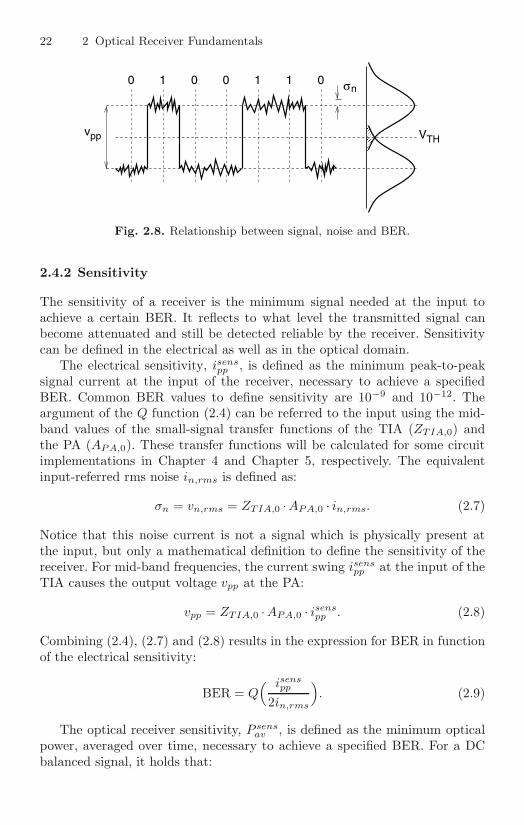
22 2 Optical Receiver Fundamentals
��������������������
��������������������
THV
0 1 0 0 1 1 0
vpp
σn
Fig. 2.8. Relationship between signal, noise and BER.
2.4.2 Sensitivity
The sensitivity of a receiver is the minimum signal needed at the input toachieve a certain BER. It reflects to what level the transmitted signal canbecome attenuated and still be detected reliable by the receiver. Sensitivitycan be defined in the electrical as well as in the optical domain.
The electrical sensitivity, isenspp , is defined as the minimum peak-to-peak
signal current at the input of the receiver, necessary to achieve a specifiedBER. Common BER values to define sensitivity are 10−9 and 10−12. Theargument of the Q function (2.4) can be referred to the input using the mid-band values of the small-signal transfer functions of the TIA (ZTIA,0) andthe PA (APA,0). These transfer functions will be calculated for some circuitimplementations in Chapter 4 and Chapter 5, respectively. The equivalentinput-referred rms noise in,rms is defined as:
σn = vn,rms = ZTIA,0 ·APA,0 · in,rms. (2.7)
Notice that this noise current is not a signal which is physically present atthe input, but only a mathematical definition to define the sensitivity of thereceiver. For mid-band frequencies, the current swing isens
pp at the input of theTIA causes the output voltage vpp at the PA:
vpp = ZTIA,0 ·APA,0 · isenspp . (2.8)
Combining (2.4), (2.7) and (2.8) results in the expression for BER in functionof the electrical sensitivity:
BER = Q( isens
pp
2in,rms
). (2.9)
The optical receiver sensitivity, P sensav , is defined as the minimum optical
power, averaged over time, necessary to achieve a specified BER. For a DCbalanced signal, it holds that:

2.5 Intersymbol Interference 23
time
0
RV
inV
out
VTH
t1 t2
vpp
C
(a)
(b)time
1 0 0 01 1 1
1 1 1 10 0
Fig. 2.9. Effect of low-pass filtering on binary data: (a) periodic data, (b) randomdata.
P sensav =
isenspp
2R, (2.10)
where R is the responsivity of the photodiode (3.4) and expressed in A/W.This leads to a third expression for the BER:
BER = Q(P sens
av ·Rin,rms
). (2.11)
In the measurements of Chapter 6, the optical sensitivity for a certain BERwill be used, rather than the electrical sensitivity. After all, optical signals areapplied at the input and can be measured directly.
2.5 Intersymbol Interference
Not only noise reduces the quality of the eye diagram, also bandwidth limi-tations have impact on the eye opening. This type of degradation is knownas intersymbol interference (ISI). The effect of both low-pass filtering andhigh-pass filtering are discussed.
2.5.1 Low-Pass Filtering
In order to study the effect of the finite bandwidth of circuits, the signalquality at the output of a first order low-pass filter is examined. As shownin Fig. 2.9, the filter simply consists of resistor R and capacitor C. The 3-dBbandwidth f3dB of this filter is given by:
f3dB =1
2πRC. (2.12)
When a periodic square wave is applied at the input, the output signal con-sists of rising and falling exponential waves, with time constant τ = RC (see

24 2 Optical Receiver Fundamentals
Vin
Vout
C
01
R
timetime
1 1 110 1
Fig. 2.10. Effect of high-pass filtering on random binary data.
Fig. 2.9(a)). This means that for time t = τ , the output has risen or fallen to63 % of its final value. If the bit period Tb is large enough compared to τ , theexponential tail has vanished and the peak-to-peak value of the binary datais large enough to be detected without any errors.
Considering random data in Fig. 2.9(b), the output does not attain theupper or lower levels which define vpp at the end of every bit period. For twoconsecutive ones or zeros, it does, but for a single one followed by a singlezero (or vice versa), it doesn’t. This is undesirable because the output voltagelevels corresponding to ones and zeros vary with time, making it difficult todefine a decision threshold VTH . For example, the levels at t = t1 and t = t2are more susceptible to noise and can be misinterpreted by the detector. Thisphenomenon is called intersymbol interference (ISI), because the exponentialresponse during one bit period corrupts the signal levels produced for subse-quent bits. The narrower the bandwidth, the longer the exponential tails andthe greater the ISI.
2.5.2 High-Pass Filtering
To understand the effect of high-pass filtering, suppose a random binary se-quence is applied to the first-order high-pass filter with capacitor C and resis-tor R (see Fig. 2.10). The low-frequency cut-off, or the frequency where thegain is 3 dB lower than its high-frequent value, is given by:
fLF =1
2πRC. (2.13)
Such a low-frequency cut-off appears in the receiver response for instancewhen ac coupling is used between TIA and PA, or when offset compensationis used in the PA (Chapter 5).
Fig. 2.10 shows that each transition at the input immediately appears atthe output, but when receiving a long string of ones or zeros, the outputvoltage drifts. As a result, the bits after each long run suffer from a large(temporary) DC shift, making it difficult to set a decision threshold VTH .This phenomenon can also be viewed as ISI, because each bit level dependson the preceding pattern.

2.6 Jitter 25
VTH
jitter
Fig. 2.11. Jitter definition.
The above effect is called baseline wander or DC wander, because the ‘in-stantaneous’ DC value of the output waveform changes randomly. To minimizebaseline wander, τ = RC must be sufficiently larger than the longest possibledata run of ones or zeros.
2.6 Jitter
So far we have discussed how noise and ISI affect the signal levels at thedecision circuit. However, the decision process not only involves the signalvoltage, but also the signal timing. The deviations of the threshold voltageVTH crossings from their ideal position in time is called jitter (Fig. 2.11).Jitter may influence the optimal sampling instant of the decision circuit. Justlike noise and ISI, too much jitter closes the eye opening and introduces biterrors.
The total jitter may be composed of deterministic jitter and random jitter.Examples of deterministic jitter are data-dependent jitter and duty-cycle dis-tortion jitter. Data-dependent jitter is produced when the signal edge movesslightly in time, depending on the values of the surrounding bits. It can becaused for example by an insufficient bandwidth or by baseline wander dueto an insufficient low-frequency cut-off. Duty-cycle distortion jitter occurs ifthe rising and falling edges do not cross each other at the decision thresholdvoltage. Random jitter is, in contrast to deterministic jitter, not related toany data pattern or any deterministic cause. It is produced, for example, bynoise on edges with a finite slew rate. It can also be caused by carrier mobilityvariations due to instantaneous temperature fluctuations.
Besides the data jitter described above, also clock jitter exists. This jitteris important in the clock and data recovery circuit where the decision processtakes place. For instance, if the sampling instant of the decision circuit varieswith time, an increase in BER might occur. In the frequency domain, the jittercounterpart is called phase noise. It is extremely important for the design ofoscillators and clock and data recovery circuits, but falls beyond the scope ofthis text.
26 2 Optical Receiver Fundamentals
2.7 Conclusions
Some basic concepts and definitions, needed in the remainder of this text,have been introduced in this chapter. First, two systems have been studiedwhich both contain an optical receiver front-end: a transceiver for opticalcommunication systems and a pickup unit for optical storage systems. Next,the data which will be applied at the input of the receiver circuits has beenpresented: continuous mode non-return-to-zero pseudorandom binary data.An efficient representation of this data is the eye diagram, and it will be usedfrequently to study the data quality at the output of the receiver. Finally, threephenomena have been studied which reduce the eye opening and introduce biterrors: the receiver noise, the limited receiver bandwidth and jitter.

3
Standard CMOS Photodiodes
3.1 Introduction
This chapter discusses the first component of the optical receiver, the pho-todetector. It deviates from subsequent chapters, as no integrated circuits arediscussed and no transistors are shown in the figures. However, the optical andelectrical properties of the photodiode impose important requirements on thedesign of the next blocks of the receiver chain. Therefore, this chapter is com-pletely dedicated to the light detection mechanisms involved using reverselybiased silicon pn-junctions.
Section 3.2 starts with the basic definition of a photon, to end with themost relevant characteristics of the photodiode: responsivity and speed. Mo-tivation is provided for the integration of photodetectors in a non-optimized,mainstream CMOS technology. By means of illustration, an overview of someinteresting monolithic opto-electrical receivers is given in Section 3.3. Not onlyCMOS implementations are considered, but also BiCMOS and SOI implemen-tations.
To gain in-depth understanding of the photodetection mechanisms, a one-dimensional model, based on semiconductor physics equations, is worked outin Section 3.4. Because this model has its limitations, a two-dimensional modelis developed with MEDICI. This model is discussed in Section 3.5. The speedand responsivity performance of several diode topologies are compared, andthe influence of technology scaling and illumination with different light wave-lengths are studied. The results and trends predicted by these simulationscorrespond well with other photodiode modeling papers which can be foundin open literature: [Pal01, Gen01, Rad03, Rad05].
3.2 Basic Concepts
In an optical communication system, the light generated by a laser diode isconverted to an electrical signal at the receive end by means of a photodiode.
27

28 3 Standard CMOS Photodiodes
Various properties of photodiodes affect the sensitivity and speed of the re-ceiver front end. This section discusses some basic definitions to characterizethe performance of a photodiode. Also the pro’s and con’s of using a main-stream CMOS technology are discussed.
3.2.1 Principles of Light Detection
As shown by Albert Einstein in 1905, light behaves not always as a continuouswave. Under certain circumstances, light acts as a stream of discontinuous,individual particles. These particles, or “light quanta,” (later named photons)each carry a “quantum,” or fixed amount of energy, given by:
Ep = hν =hc
λ. (3.1)
h = 6.63 ·10−34 J · s is Planck’s constant, ν is the frequency of the electro-magnetic wave, c = 3 · 108 m/s is the speed of light in vacuum and λ is thecorresponding wavelength. The higher the frequency or the smaller the wave-length, the more energy per photon or the less photons for a given total energy.
Light detection can be performed by a reversely biased junction, as shownin Fig. 3.1. When the junction is illuminated with light, incident photons withan energy larger than or equal to the bandgap energy Eg of the semiconductormaterial generate electron-hole pairs. Fundamental absorption of photons withan energy smaller than Eg is not possible. Consequently, the semiconductoris transparent for light with wavelengths longer than:
λc =hc
Eg. (3.2)
For silicon, Eg = 1.12 eV, which means that only light with wavelengthsshorter than 1.1 µm can be detected with silicon photodiodes.
The electrons and holes generated in the depletion region (or space chargeregion SCR) are separated by a large electric field and drift in opposite direc-tions. The transport mechanism of the carriers generated outside the depletionregion is diffusion, which is a slow transport mechanism compared to drift.These carriers may recombine before they are detected, or they diffuse inwardand are collected across the junction, adding a slow tail to the photodiode’stime response. To prevent the recombination loss of generated carriers andto have a fast diode response, efficient photodiode operation demands a largedepletion region.
The absorption coefficient α determines how deep light of a particularwavelength penetrates into a specific material. The intensity of light penetrat-ing into a medium decreases exponentially with depth, as given by Lambert-Beer’s Law:
Φ(x) = Φ0 · e−αx. (3.3)

3.2 Basic Concepts 29
hν
hν
hν
P NDepletion region
V
P
Valence band
Conduction band
Energy EBandgap
opt
Idio
R
Electric field
g
hole diffusiondriftdiffusionelectron
Fig. 3.1. Principle of operation of a semiconductor photodiode.
μλWavelength ( m)
Abs
orpt
ion
coef
ficie
nt
( m
)μ
−1
α
Ge
In Ga As
InP
1000
100
10
1
0.1
0.01
0.001
GaAs
0.53 0.47
Si
0.4 0.6 0.8 1 1.2 1.4 1.6 1.8
Fig. 3.2. Absorption coefficient versus wavelength for various semiconductor mate-rials [Zim04].

30 3 Standard CMOS Photodiodes
Φ(x) is the light flux ( photons/(cm2 · s)) at depth x in the material whileΦ0 is the initial flux. The absorption coefficient versus wavelength is de-picted in Fig. 3.2 for the most important semiconductor materials [Zim04].In0.53Ga0.47As and Ge cover the widest range of wavelengths, including 1.3 µmand 1.54 µm, which are used for long distance optical fiber communication.The absorption coefficients of GaAs and InP are high in the visible spectrum(≈ 400 nm–700 nm). Silicon detectors are appropriate for the visible and in-frared spectral range. The absorption coefficient of silicon is however one ortwo orders of magnitude smaller than that of the direct semiconductors InPand GaAs. The inverse of the absorption coefficient, 1/α, is called the pene-tration depth, and will be used frequently in this text.
The diode current Idio, consisting of photo-generated carriers, is linearlyproportional to the optical power Popt:
Idio = R ·Popt. (3.4)
R is called the responsivity of the diode. Typical values for commercially avail-able infrared photodiodes are 0.5 A/W to 0.8 A/W. In an ideal photodiode,every photon entering the device generates an electron-hole pair. In reality,however, some photons are reflected from the surface or absorbed by the ma-terial to produce heat. The quantum efficiency of the photodiode is the ratioof the number of electrons generated, and the number of photons applied:
η =Idio/q
Popt/(hc/λ)(3.5)
= Rhc
qλ(3.6)
=1.24λ
R. (3.7)
Besides responsivity, speed is an important parameter of the photodiode.As already mentioned before, the slowly diffusing carriers add a tail to thediode’s time response. For example, the diffusion time of a hole through 10 µmof silicon is 40 ns [Mil79]. So for high-speed operation, the depletion regionhas to be sufficient wide, preferably wider than the penetration depth 1/α.Due to the high electrical field over the junction, the carriers attain theirsaturation velocity, which is approximately 107 cm/s in silicon [Mil79]. Con-sequently, the transit time can be very short, for instance 0.1 ns for a 10 µmwide junction. Having a depletion region that encloses the absorption regionis also the requirement for high quantum efficiency, as diffusing carriers mightrecombine before detection. In Sections 3.4 and 3.5, the intrinsic speed per-formance of CMOS photodiodes will be characterized by the 90 % rise time ofthe step response, the (intrinsic) frequency characteristic and the (intrinsic)bandwidth.
Finally, another important characteristic of the photodiode is its parasiticjunction capacitance. As will be explained in Section 4.3.1, its value combined

3.2 Basic Concepts 31
with the input impedance of the receiver, determines an RC constant whichlimits the bandwidth in most circuits. This bandwidth is often called theextrinsic bandwidth, to distinguish from the intrinsic bandwidth. The junctioncapacitance is thus of uttermost importance for the transmission speed that isachievable with a photodiode-receiver combination. Its value is dependent ondoping concentrations, reverse voltage, and diode area. Note that the latter ismostly one of the only degrees of freedom available in the design of a standardCMOS photodiode, as doping levels and the maximum supply voltage are fixedby the technology.
3.2.2 The Use of Standard CMOS
As mentioned in Chapter 1, there exists a wide range of emerging applica-tions where optical receivers are needed. Especially, for these applications,cost aspects are crucial. This is the main motivation for choosing a CMOStechnology: in the end, CMOS is cheap. Of course, today’s 65 nm CMOS tech-nologies are expensive. But in a few years, when all digital standard cells areimplemented in nm-scale technologies, the high manufacturing cost will bejustified by the large production volumes.
Using standard CMOS for light detection has the main disadvantage thatthe technology is not optimized for optical devices. First, the width of thejunctions doesn’t match the penetration depth of light. Second, the reversevoltage available to bias the junctions cannot be higher than the supply volt-age. Finally, no postprocessing is allowed, so no anti-reflective coatings areused. These limitations result in photodiodes with minor responsivity andspeed performance compared to commercially available diodes. To circum-vent these difficulties and to implement cheap but high-performing opticalreceivers are the main objectives of this work.
Besides the low cost aspect, the integration of photodiodes in standardCMOS has even more benefits. The integration of the photodiode on the samedie as the receiver causes a reduction of the external components count, re-sulting in a low-cost system with enhanced yield. Furthermore, an integratedphotodiode reduces the total input capacitance by eliminating the parasiticsdue to the diode’s package, the PCB wiring, the IC-package and some bond-pads. As will become clear in Section 4.3.1, this gives the opportunity toincrease the transimpedance-bandwidth product for free. A side effect is thatthe diode capacitance increases as technology scales down, but this will betreated in more detail in Section 3.5.5. Finally, a major advantage of an in-tegrated photodiode is the reduction of noise coupling into the input nodethanks to the removal of bondwires, the package pins and the PCB pathsconnected to this node, which otherwise pick up spurious signals from theenvironment.
Fig. 3.3 shows the junctions which are available in a standard CMOStechnology. The first one is an n+ p-substrate junction, the second one is ann-well p-substrate junction and the last one is a p+ n-well junction. They all
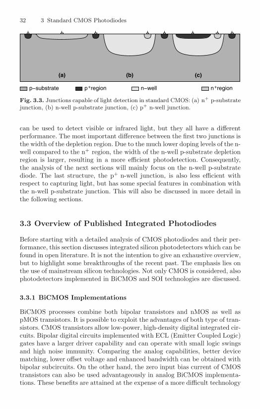
32 3 Standard CMOS Photodiodes
n−wellp region+ n region+
(a) (b) (c)
p−substrate
Fig. 3.3. Junctions capable of light detection in standard CMOS: (a) n+ p-substratejunction, (b) n-well p-substrate junction, (c) p+ n-well junction.
can be used to detect visible or infrared light, but they all have a differentperformance. The most important difference between the first two junctions isthe width of the depletion region. Due to the much lower doping levels of the n-well compared to the n+ region, the width of the n-well p-substrate depletionregion is larger, resulting in a more efficient photodetection. Consequently,the analysis of the next sections will mainly focus on the n-well p-substratediode. The last structure, the p+ n-well junction, is also less efficient withrespect to capturing light, but has some special features in combination withthe n-well p-substrate junction. This will also be discussed in more detail inthe following sections.
3.3 Overview of Published Integrated Photodiodes
Before starting with a detailed analysis of CMOS photodiodes and their per-formance, this section discusses integrated silicon photodetectors which can befound in open literature. It is not the intention to give an exhaustive overview,but to highlight some breakthroughs of the recent past. The emphasis lies onthe use of mainstream silicon technologies. Not only CMOS is considered, alsophotodetectors implemented in BiCMOS and SOI technologies are discussed.
3.3.1 BiCMOS Implementations
BiCMOS processes combine both bipolar transistors and nMOS as well aspMOS transistors. It is possible to exploit the advantages of both type of tran-sistors. CMOS transistors allow low-power, high-density digital integrated cir-cuits. Bipolar digital circuits implemented with ECL (Emitter Coupled Logic)gates have a larger driver capability and can operate with small logic swingsand high noise immunity. Comparing the analog capabilities, better devicematching, lower offset voltage and enhanced bandwidth can be obtained withbipolar subcircuits. On the other hand, the zero input bias current of CMOStransistors can also be used advantageously in analog BiCMOS implementa-tions. These benefits are attained at the expense of a more difficult technology

3.3 Overview of Published Integrated Photodiodes 33
development and at the expense of more complex chip-manufacturing tasks,leading to longer chip-fabrication time and higher costs [Zim04].
The bipolar npn transistor is formed by an n+-emitter, a p-type base, andan n-type collector. To minimize collector series resistance, the collector notonly consists of an epitaxial n−-layer, but also has a buried n+-subcollectorand n+-collector plugs. Without any process modifications, the buried n+-subcollector can serve as the cathode, the n-collector epitaxial layer can serveas the intrinsic region of a PIN diode, and the p-base implant can serve asthe anode. The main advantage of a PIN diode is its lowly doped intrinsicregion where a high electric field is present if it is depleted. In this region,carrier transport is drift, which results in fast and efficient photodetectors.This is especially true if the intrinsic region corresponds to the light penetra-tion depth. For 800 nm wavelengths, a thickness of at least 10 µm is necessarydue to the low optical absorption coefficient (Fig. 3.2). Such a large intrinsiclayer thickness requires a severe reduction of the epitaxial layer concentrationto obtain a spreading of the electric field over the entire intrinsic zone. How-ever, this would destroy the bipolar transistor performance. Therefore, processmodifications are needed to optimize the performance of both the integratedphotodiode (which needs a thick, lowly doped intrinsic layer) and the bipolartransistor (which needs a thin, higher doped n-collector).
In [Stu05], a dedicated 0.5 µm BiCMOS technology that combines high-speed transistors with an integrated PIN photodiode is described. The avail-able devices are a single-poly npn bipolar transistor with ft=20 GHz, a ver-tical pnp bipolar transistor with ft=1 GHz, standard 0.5 µm CMOS, andpassive devices like capacitors, resistors and laser fuses. The integrated PINphotodiode is optimized concerning speed and sensitivity for all three lightwavelengths used for optical data storage, like CD (780 nm), DVD (660 nm)and Blu-ray (405 nm). The measured photodiode sensitivity is 0.35 A/W,0.4 A/W, and 0.25 A/W for 780 nm, 660 nm and 405 nm wavelengths respec-tively. The 3-dB small signal intrinsic bandwidth of the photodiode is above1 GHz.
This technology has been used to implement an optical receiver IC forCD, DVD, and Blue-Laser optical data storage applications [Stu04], [Stu05].It includes a new architecture of high-speed and low-noise variable gain tran-simpedance amplifiers with current preamplifier input. The amplifier tran-simpedance gain is programmable over a range of 130 Ω to 270 kΩ by a serialinterface. The amplifier small-signal bandwidth is 260 MHz for the highestgain, which gives a transimpedance-bandwidth product of 70 THzΩ. A re-design of this chip with some new developments is presented in [Sei05]. Theobtained improvements are a reduction of the power consumption, the diearea, the offset voltage, an increase of the sensitivity, 1.5 V output swing anda drive capability of a 10 pF/10 kΩ output load. An overall transimpedanceof 465 kΩ leads, with the responsivity of the photodiode, to a sensitivity of186 mV/µW for 660 nm light with a 3-dB bandwidth of 145 MHz. Compared

34 3 Standard CMOS Photodiodes
with the previous IC, sensitivity is improved by a factor of 1.8, while band-width is decreased by the same factor.
The same technology has been used to implement OEIC’s for high-speedoptical interconnects between or within electronic systems. The wavelengthregion of interest now is 600 nm to 850 nm. In [Swo03] an optical receiver witha maximum possible data rate of 1.8 Gbit/s is presented. This is achievedby using a bias voltage of 17 V (instead of the supply voltage of 5 V) atthe cathode of the photodiode, to increase the electric field strength in theintrinsic region and enhance the diode speed performance. Using 670 nm light,a sensitivity of −21.9 dBm for a BER of 10−9 is measured. The next step is tointegrate a voltage-up-converter (VUC) with the OEIC, which generates on-chip the higher cathode voltage from the 5 V supply voltage. This is presentedin [Swo04], where the VUC produces a voltage of 11 V and improves thebandwidth of the OEIC from 1.5 GHz to 2.4 GHz. For a data rate of 3 Gbit/sand a BER of 10−9, a sensitivity of −24.3 dBm at a wavelength of 660 nmis obtained. In [Swo05], measurement results at 4 Gbit/s and 5 Gbit/s areadded. Finally, [Swo06] presents a 11 Gbit/s integrated receiver for 850 nmwavelength. A reverse photodiode voltage of 17 V extends the diode 3dB-frequency to 2.2 GHz. To enable high-speed data reception above 4 Gbit/s,the frequency response of the diode must be corrected with the help of ananalog equalizer, first introduced by [Rad04]. At 11 Gbit/s a minimum opticalpower of −8.9 dBm is needed for a BER of 10−9.
3.3.2 SOI Implementations
Silicon on Insulator (SOI), developed by IBM, is a chip-making technologythat builds transistors on a very thin layer of silicon, improving chip per-formance and reducing power consumption. A thin, insulating layer, such assilicon oxide or glass, is placed between the thin layer of silicon and the siliconsubstrate. This process helps to reduce the amount of electrical charge thata transistor has to move during a switching operation, thus making it fasterand allowing it to switch using less energy. SOI chips can be as much as 15percent faster and use 20 percent less power than today’s bulk CMOS-basedchips. SOI chips tend to cost more than their standard silicon counterparts,so SOI has been primarily used for high-end applications [Fre].
Photodetectors implemented in a thin SOI layer might be attractive, be-cause light with a long wavelength (and long penetration depth) generatescarriers in the silicon substrate wafer, which is isolated from the device SOIlayer by the buried oxide. Therefore, SOI avoids the slow diffusion currentknown from photodiodes in bulk silicon. In [Csu02], the optical receiver ismanufactured on 2 µm thick SOI substrates with a high resistivity. The thick-ness of the SOI is chosen to achieve a compromise between quantum efficiencyand bandwidth for the photodiodes. The receiver is implemented in a 130 nmCMOS process flow. The n- and p-type regions of the lateral interdigitated

3.3 Overview of Published Integrated Photodiodes 35
PIN diode is formed by standard nMOS and pMOS drain and source implan-tations. A sensitivity of −10.9 dBm is obtained for a bitrate of 5 Gbit/s at aBER of 10−9.
In [Yan03], the same photodiode is wire-bonded to a 10 Gbit/s SiGe TIAthat was fabricated in a 0.18 µm BiCMOS technology. By applying a higherreverse voltage, the photodiode operates in avalanche gain mode. Owing toimpact ionization, photocurrent gain is observed. For a bias voltage > 20 V,the 3-dB optical bandwidth is greater than 8 GHz. The complete receiverachieves a sensitivity of −6.9 dBm (BER < 10−9) at 10 Gbit/s.
3.3.3 CMOS Implementations
As will become clear in the next sections, the main limitations of standardsubmicron CMOS photodiodes are caused by the diffusing substrate carriers.Many attempts exist in literature to overcome this problem. In [Ing04], therelative part of the drift current to the total current is optimized by usingthe side-wall capacitance of the n-well p-substrate junction. Although thecorresponding depletion region is thin too, its depth perpendicular to thesurface is larger compared to the depth of the bottom-plate capacitance. Themajor disadvantage of this approach is the limited photodiode’s responsivitydue to the overhead required to connect the diode. Measurements on theside-wall photodiode have been done with a 650 nm LED as light source.With the network analyzer, a flat response is obtained up to approximately40 MHz. This pole would be caused by the LED rather than by the integratedphotodiode.
A first breakthrough in the integration of high-speed submicron CMOSphotoreceivers was presented by [Woo98]. The 0.35 µm receiver integratesa photodiode, preamplifier, digital logic, and off-chip driver. The n-well re-gion in which the detector was made measures 16.54 µm x 16.54 µm, andis surrounded by a grounded p+ guard ring. Inside the n-well an interdigi-tated network of p-diffusion fingers forms the active terminal of the detector.The photodetector responsivity, using 850 nm light, ranges from 0.01 A/W to0.04 A/W near junction breakdown (10 V). Under these bias conditions andat a bitrate of 1 Gbit/s, a BER of 10−9 is obtained with an average opticalinput power of −6.3 dBm.
Another way to circumvent the problem of diffusing substrate carriers isproposed by [Roo00]. The spatially modulated light (SML) detector consistsof a row of rectangular p−-n junctions (fingers) alternatingly covered and non-covered with a light blocking metal. The masked fingers connected togetherform the deferred detector. The other fingers connected together form the im-mediate detector. When a light pulse is incident on the detector, carriers aregenerated below the immediate zone and not below the masked deferred zone.The photo-generated carriers are spatially modulated. The immediate detec-tor “immediately” detects the shallow-generated carriers. The bulk-generatedcarriers diffuse in all directions and most of them will finally reach a detector

36 3 Standard CMOS Photodiodes
junction (as well in the deferred as in the immediate zone). If the responseof the deferred detector is subtracted from the response of the immediatedetector, a fast response is achieved as the influence of the slow diffusing car-riers is cancelled. This SML-detector is integrated with a low-offset receiverin a 0.6 µm standard CMOS technology [Roo00]. The sensitivity at a BERof 10−9 is −18 dBm (λ = 860 nm) for 250 Mbit/s. A later realization in a0.25 µm CMOS technology [Roo01] achieves, at 700 Mbit/s, a BER of 10−12
for the same input power. The receiver with SML-detector proposed by [Jut05]is integrated in an unmodified 0.18 µm CMOS technology. At 2 Gbit/s andusing 850 nm light, the sensitivity equals −8 dBm at a BER of 10−9.
A totally different approach to enhance the speed of integrated CMOS de-tectors is introduced by [Rad04, Rad05]. Not the n-well photodiode topologyis changed, but a clever circuit solution is proposed. Following device simula-tions, the overall intrinsic photodiode frequency response shows a slow decaystarting in the low MHz range. The roll-off in the overall photocurrent responseis only about 5 dB/decade for frequencies between roughly 10 MHz and thelower GHz range. So the signals from the photodiode are low bandwidth (MHzrange) but still relatively strong at very high frequencies (GHz range). There-fore an analog equalizer is introduced that compensates (in gain and phase)for the diode photocurrent roll-off in the range from 1 MHz to 1 GHz. Becauseno photogenerated carriers are drained away or subtracted from each other,the author claims there is no sensitivity or responsivity penalty. This results ina measured 3 Gbit/s data rate with a low BER (< 10−9) at −19 dBm 850 nmoptical input power.
3.3.4 Conclusions
The main focus in this literature overview lies on the performance of thephotodiodes and the overall speed/sensitivity performance of the optical re-ceivers that they are part of. One important conclusion is that, to the presentday, there exists no uniform way to measure and report the characteristicsof the opto-electrical receiver. For instance, [Stu05] and [Sei05] express thesensitivity in mV/µW (which is simply the product of responsivity and tran-simpedance gain). On the other hand, the sensitivity in for example [Swo04] isthe minimum average optical input power needed to achieve a BER of 10−9.Also the use of different wavelengths makes a fair comparison more difficult(the BiCMOS implementations mostly use 660 nm light, while the CMOS im-plementations almost all apply 850 nm light). Finally the speed of the receiveris expressed in different ways: some authors (like [Stu05], [Sei05]) emphasizethe bandwidth of the amplifying circuit, while others focus on the bitrate ofthe received data (like [Roo00], [Rad05]).
However, the general trends which can be concluded from this overvieware:
• The photodiodes implemented in BiCMOS achieve the best performance.The main reason is that the technology used in for example [Stu05, Swo06]

3.4 One-Dimensional Model 37
is enhanced to ameliorate both responsivity and intrinsic speed of thephotodiode. A higher performance is achieved at the expense of a moreexpensive technology.
• SOI does not offer large advantages over CMOS: comparing [Csu02]with [Rad05], the first achieves higher bitrates (5 Gbit/s versus 3 Gbit/s),but the latter has a better sensitivity (−19 dBm versus −10.9 dBm, bothfor a BER of 10−9).
• The main challenge in standard CMOS remains the realization of a pho-todiode with a high intrinsic speed, combined with a large responsivity.This trade-off will be worked out in more detail in the following sections.Several approaches, like [Roo00] and [Rad05] have increased the intrinsicspeed so that the speed performance becomes comparable to the perfor-mance of the BiCMOS detectors. However, the sensitivity of the latterones remains unbeatable.
3.4 One-Dimensional Model
In this section, a one-dimensional model is developed to analyze the lightdetection performance of standard CMOS junctions. It is based on the basicequations of semiconductor physics [Ove98]. The model helps to gain insight inthe basic working principles, but should also be treated with care, as it is onlya one-dimensional model. To interpret the analytical results, the parametersof a 90 nm CMOS technology are used. The principles and major conclusionsof this model have been published in [Her03].
3.4.1 N-Well P-Substrate Junction
The current of this photodetector is composed of a drift current originat-ing from the carriers generated inside the depletion region (or space chargeregion SCR), an electron diffusion current from electrons generated in the p-substrate, and a hole diffusion current from holes generated in the n-well. Tocharacterize the magnitude and speed of the total current step response, theconcentration of the minority carriers in n-well and p-substrate has to be cal-culated first. Fig. 3.4 shows a schematic representation of the one-dimensionalmodel.
Diffusion of Holes in the N-Well
The continuity equation of the holes in the n-well, which is a non-homogeneouspartial differential equation, is given by:
∂p(x, t)∂t
= Dp∂2p(x, t)
∂x2− p(x, t) − p0
τp+ αΦe−αx. (3.8)

38 3 Standard CMOS Photodiodes
������������������������������������������������������������������������������������������������������������������������������������������������������������������������������������������������������������������������������������������������������������������������������������������������������������������������������������������������������������������������������������������������
������������������������������������������������������������������������������������������������������������������������������������������������������������������������������������������������������������������������������������������������������������������������������������������������������������������������������������������������������������������������������������������������
Lscr
Lb
Lnw
������������ SCRn−well
0
xp−substrate
Fig. 3.4. One-dimensional model of the n-well p-substrate junction.
Following list gives an explanation of all variables:
x deptht timep hole concentrationp0 initial hole concentrationDp hole diffusion constantτp hole minority carrier lifetimeα absorption coefficient of light in SiΦ photon flux
According to (3.8), the carrier concentration within an elementary volume canonly change as a function of time if there is a difference between the incomingand outgoing carrier fluxes (due to diffusion currents, first term), or a netrecombination (second term) or generation (third term). The boundary andinitial conditions are:
p(x = 0, t) = p0, (3.9)p(x = Lnw, t) = 0, (3.10)
p(x, t = 0) = p0. (3.11)
The boundary equation (3.9) states that at the surface (x = 0), the concen-tration equals the initial concentration p0. This assumption has been madefor simplicity, as in reality impurities at the oxide-silicon interface create in-terface states and a netto recombination. At the edge of the space chargeregion (x = Lnw) carriers are swept away, so the minority carrier concen-tration equals zero (3.10). When no light penetrates the junction, condition(3.11) defines that the hole concentration equals the initial concentration p0.

3.4 One-Dimensional Model 39
To solve the mathematical problem of (3.8), the non-homogeneous partialdifferential equation is split up in a homogeneous partial differential equationand a non-homogeneous ordinary differential equation, which are mathemati-cally easier to handle. The solution p(x, t) is separated in a time-independentpart v(x) and a time-dependent part w(x, t):
p(x, t) = v(x) + w(x, t). (3.12)
The solution of (3.8), which describes the variation of the holes in the n-wellwith respect to depth and time, is thus given by:
p(x, t) = p0 − αΦ
Dpα2 − 1/τpe−αx
+ Ap exp
(x√Dpτp
)+ Bp exp
(−x√Dpτp
)
+∞∑
k=1
Cp(k) sin(
kπx
Lnw
)exp
(−
(k2π2Dp
L2nw
+1τp
)t
). (3.13)
Ap, Bp and Cp(k) are constants which can be determined by solving theboundary and initial conditions (3.9)–(3.11).
The hole diffusion current as a function of time is proportional to thegradient of the minority carrier concentration at the edge of the space chargeregion:
Jdiffp = −qDp∂p
∂x
∣∣∣∣∣x=Lnw
, (3.14)
where q is the elementary charge and Dp the hole diffusion constant.
Diffusion of Electrons in the P-Substrate
The continuity equation of the electrons in the p-substrate is similar to (3.8)and given by:
∂n(x, t)∂t
= Dn∂2n(x, t)
∂x2− n(x, t) − n0
τn+ αΦe−αx. (3.15)
Following list gives an explanation of all variables:
x deptht timen electron concentrationn0 initial electron concentrationDn electron diffusion constantτn electron minority carrier lifetime

40 3 Standard CMOS Photodiodes
α absorption coefficient of light in SiΦ photon flux
The boundary and initial conditions now are:
n(x = Lscr, t) = 0, (3.16)n(x = Lb, t) = n0, (3.17)n(x, t = 0) = n0. (3.18)
The first boundary condition (3.16) declares that the concentration equalszero at the edge of the space charge region (x = Lscr). At distance x = Lb, thephoto-generated minority carriers which are diffusing have negligible effect onthe equilibrium minority carrier concentration n0, which results in condition(3.17). Lb depends both on lifetime of the diffusion carriers and the penetra-tion depth of light in the material. At the initial state, there is no light input,so the concentration equals the initial concentration n0 (3.18).
The solution of this non-homogeneous partial differential equation (3.15)is found in an analogue way as for the holes, and the solution is given by:
n(x, t) = n0 − αΦ
Dnα2 − 1/τne−αx
+ An exp(
x√Dnτn
)+ Bn exp
( −x√Dnτn
)
+∞∑
k=1
Cn(k) sin(
kπ(x − Lscr)(Lb − Lscr)
)exp
(−
(k2π2Dn
(Lb − Lscr)2+
1τn
)t
).
(3.19)
An, Bn and Cn(k) are constants which again can be determined by solvingthe boundary and initial conditions (3.16)–(3.18).
Like (3.14), the electron diffusion current as a function of time is propor-tional to the gradient of the minority carrier concentration at the edge of thespace charge region:
Jdiffn = qDn∂n
∂x
∣∣∣∣∣x=Lscr
, (3.20)
where q is the elementary charge and Dn the electron diffusion constant.
Drift in the Space Charge Region
The drift current in the space charge region is given by:
Jdrift = q
∫ x=Lscr
x=Lnw
G(x)dx,
= q
∫ x=Lscr
x=Lnw
αΦe−αxdx. (3.21)

3.4 One-Dimensional Model 41
G(x) is the generation term due to penetrating light with flux Φ and absorp-tion coefficient α, which also appears in continuity equations (3.8) and (3.15).Lscr − Lnw is the width of the space charge region and determined by:
Lscr − Lnw =
√2εSi
q
NA + ND
NAND(Vbi − VR). (3.22)
NA is the concentration of acceptors in the p-substrate, ND is the concentra-tion of donors in the n-well, εSi is the permittivity of Si, q is the elementarycharge, Vbi is the technology-dependent built-in voltage and VR is the reversevoltage of the junction. The space charge region becomes wider when dopingconcentrations are lowered or when the reverse voltage VR is increased.
Graphical Representation of the Results
After derivation of the mathematical equations, it is time to visualize andinterpret the results. The diode, with the cross section of Fig. 3.4, has anarea of 100 µm x 100 µm and is illuminated with a step input of 1 µW. Theminority carrier lifetimes in the n-well and in the p-substrate are assumed to be1 µs. To investigate the influence of wavelength, two different wavelengths areapplied: 600 nm and 800 nm. This directly influences the absorption coefficientα as well as the initial light flux Φ0. For red 600 nm light, α equals 5000 cm−1
and Φ0 corresponds to 3 · 1016 photons/(cm2 · s). When infrared 800 nm lightis applied, α drops to 1000 cm−1 while Φ0 becomes 4 · 1016 photons/(cm2 · s).The reverse voltage over the junction is only 0.5 V, which is half the availablepower supply in a 90 nm CMOS technology.
Fig. 3.5 shows the concentration of minority carriers in the n-well andp-substrate versus time and depth into the substrate. The influence of wave-length is clear: a longer wavelength results in a larger penetration depth 1/α,and more carriers which are generated in the substrate. In Fig. 3.5(a), themaximum of the electron concentration is 2.1 · 1011 cm−3 at 7 µm, while inFig. 3.5(b) the maximum equals 1.7 ·1012 cm−3 at 17 µm. The maximum ofthe hole concentration lies in both cases at one half of the n-well depth (Lnw/2)and equals 1.6 ·1011 cm−3 respectively 5.7 · 1010 cm−3. The large discrepancybetween electron and hole maxima explains why the hole concentration ishardly visible in Fig. 3.5(b).
The slowly varying gradient of the electron concentration in the sub-strate determines the gradually rising diffusing current Jdiffn. As depictedin Fig. 3.6, this current is the major part of the total current, but as expectedthe effect is more pronounced when longer wavelengths are used. Accordingto this model, the responsivity of the diode is 0.32 A/W and the rise timeis 19 ns when red light is applied. For infrared light, the responsivity equals0.44 A/W while the rise time is as high as 260 ns. The relative contributionof drift current Jdrift and hole diffusion current Jdiffp is much smaller in thelatter case. So the larger the wavelength, the larger the absorption depth in

42 3 Standard CMOS Photodiodes
0
2
4
x 10−3
0
100
2000
0.5
1
1.5
2
2.5
x 1011
x [cm]time [ns]
conc
entr
atio
n [c
m−
3 ]
(a)
02
46
x 10−3
0
500
10000
0.5
1
1.5
2
x 1012
x [cm]time [ns]
conc
entr
atio
n [c
m−
3 ]
(b)
Fig. 3.5. Minority carrier concentration in n-well p-substrate junction: (a)λ=600 nm, (b) λ=800 nm.
silicon, the more carriers are generated in the substrate and the slower thetime response. But the smaller the wavelength, the higher the energy per pho-ton (3.1). For the same input power, less photons penetrate the substrate andthe responsivity is lower. Gigabit operation is not yet possible with this kindof rise times, but the more accurate two-dimensional model will show thatthings are not as bad as they seem at this stage.

3.4 One-Dimensional Model 43
0 50 100 150 2000
0.5
1
1.5
2
2.5
3
3.5
time [ns]
curr
ent d
ensi
ty [m
A/c
m2 ]
maximal current density =3.2mA/cm2
t0.9
=19 ns
Jdiffn
Jdiffp
Jdrift
Jtot
(a)
0 200 400 600 800 10000
0.5
1
1.5
2
2.5
3
3.5
4
4.5
time [ns]
curr
ent d
ensi
ty [m
A/c
m2 ]
maximal current density =4.4mA/cm2
t0.9
=260 ns
Jdiffn
Jdiffp
Jdrift
Jtot
(b)
Fig. 3.6. Current densities in n-well p-substrate junction: (a) λ=600 nm, (b)λ=800 nm.
3.4.2 P+ N-Well Junction with Guard
The previous simulations have shown that the diffusing substrate carriers are aproblem for high-speed operation, certainly when infrared light is used. Oneway to overcome this problem is to consider the p+ n-well junction togetherwith the n-well p-substrate junction. If the former is used to detect the signal,the substrate contacts can act as guard to draw away the slowly diffusing

44 3 Standard CMOS Photodiodes
������������������������������������������������������������������������������������������������������������������������������������������������������������������������������������������������������������������������������������������������������������������������������������������������������������������������������������������������������������������������������������
������������������������������������������������������������������������������������������������������������������������������������������������������������������������������������������������������������������������������������������������������������������������������������������������������������������������������������������������������������������������������������
���������������������������������������������������������������������������������������������
���������������������������������������������������������������������������������������������
scr2
p region+ n−well
Lsd
Lnw
x
0
������������p−substrate SCR
Lscr1
L
Fig. 3.7. One-dimensional model of the p+ n-well junction with guard.
signals carriers in the substrate. The resulting diode response will be smaller,but also a lot faster. This idea has also been implemented successfullyin [Woo98].
The performance of this diode has been analyzed using the same physicalequations ((3.8) to (3.22)), but now there are three diffusion currents and twodrift currents. All parameters are the same as in the previous model, and theminority carrier lifetime in the p+ region is assumed to be 0.1 ns due to thevery high doping concentration in this region. A cross section of this structureis depicted in Fig. 3.7. Electrons are diffusing in the p+ region and in the p-substrate, and they give rise to the currents Jdiffn1 and Jdiffn2. The diffusingholes in the n-well generate the current Jdiffp. Carriers generated in the veryshallow space charge region between the p+ region and the n-well will formthe small drift current Jdrift1. Jdrift2, which is somewhat larger, stems fromthe light generated carriers in the wider space charge region between n-welland p-substrate. The light wavelength is 600 nm, and the reverse voltage overboth junctions is 0.5 V.
An important question for this model is: which currents will be picked upby which contacts? In a practical implementation, three electrode contacts arepresent: one for the p+ region, one for the n-well, and one for the p-substrate.The current at the n-well electrode equals the sum of the currents at theelectrodes of the p-type regions. The current at the substrate contact consistsof the substrate diffusion current Jdiffn2, drift current Jdrift2 and one part ofthe n-well diffusion current Jdiffp. Equivalently, the current at the p+ regioncontact is made up of the p+ region diffusion current Jdiffn1, drift currentJdrift1 and the other part of the n-well diffusion current Jdiffp. In this onedimensional model, we assume an equal probability for the light-generatedholes in the n-well to be trapped by either of the space charge regions. So onehalf of Jdiffp is collected by the substrate contacts, and the other half by thep+ region contacts. This simplification is true if the carriers inside the n-well

3.4 One-Dimensional Model 45
0
2
4
x 10−3
0
100
2000
0.5
1
1.5
2
2.5
x 1011
x [cm]time [ns]
conc
entr
atio
n [c
m−
3 ]
(a)
0 10 20 30 40 50 600
0.5
1
1.5
2
2.5
3
3.5
4
time [ns]
curr
ent d
ensi
ty [m
A/c
m2 ]
max current density =3.5mA/cm2
with guard =0.9mA/cm2max current density
t0.9
=13 ns
t0.9
=1.5 ns
Jdiffn1
Jdiffp
Jdiffn2
Jdrift1
Jdrift2
Jtot1
Jtot2
(b)
Fig. 3.8. (a) Minority carrier concentration and (b) current densities in p+ n-welljunction with guard, λ=600 nm.
are uniformly distributed. However, in reality, the light flux is determined byLambert-Beer’s Law (3.3) and the light-generated carriers inside the n-wellhave a decreasing exponential distribution.
The results are depicted in Fig. 3.8. Fig. 3.8(a) shows that the concentra-tion of minority carriers in the substrate is very similar to the simple n-welldiode: the maximum lies at 7 µm and equals 2.1 · 1011 cm−3. The maximumminority concentration in the n-well is 1.1 · 1011 cm−3, while the maximum
46 3 Standard CMOS Photodiodes
concentration in the p+ region is only 5.6 · 108 cm−3. This last region is notvisible in the plot, as the minority concentration is low and the region is veryshallow compared to the other regions.
All current densities in this structure are depicted in Fig. 3.8(b). Theduration of the step input is 200 ns, but to focus on the most interesting data,only the first 60 ns are shown. If the two junctions were placed parallel, theresulting performance is comparable to the performance of the simple n-wellp-substrate junction. The responsivity is 0.35 A/W and the rise time equals13 ns. But if the substrate carriers are effectively removed by the substratecontacts, the rise time is only 1.5 ns. The price to pay is a drop in responsivity,which is now only 0.09 A/W.
By applying a one dimensional analysis, this example shows that usingthe appropriate diode structure can alleviate the problem of the diffusingminority carriers in the substrate. Also the trade-off between sensitivity andspeed, which will reappear several times in this work, is demonstrated forthe first time. However, as junctions are located closer to the surface and theside-wall capacitances become more and more important, a more accuratetwo-dimensional model is needed. This will be discussed in the next section.
3.5 Two-Dimensional Model
A two-dimensional analysis of different photodiode topologies is performedwith the device simulation program Medici [Syn]. It is a powerful tool thatcan be used to simulate the behavior of MOS and bipolar transistors, andother semiconductor devices (such as diodes). It models the two-dimensionaldistributions of potentials and carrier concentrations in a device. A number ofphysical models are incorporated into the program for accurate simulations,including models for recombination, photogeneration, mobility and lifetime.The optical Device Advanced Application Module is used to model propaga-tion of light inside and outside a device.
This section discusses three photodiode structures implemented in a0.18 µm standard CMOS technology: the classical n-well diode, the p+ n-welldiode with guard and the differential diode. Also the influence of changing thelight wavelength is studied. Finally, the effect of technology downscaling onthe photodiode performance is investigated. Most of these results have beenpresented in [Her03, Her04b, Her06a].
3.5.1 Classical N-Well Diode
Fig. 3.9 shows a schematic representation of the simulated n-well diode. As amultimode fiber has a core diameter of 50 µm or 65 µm, the dimensions of thediode are 80x80 µm2. This could be implemented as one large n-well region,or several smaller parallel n-well regions separated by substrate contacts tominimize substrate resistance. The amount of squares per diode side is given
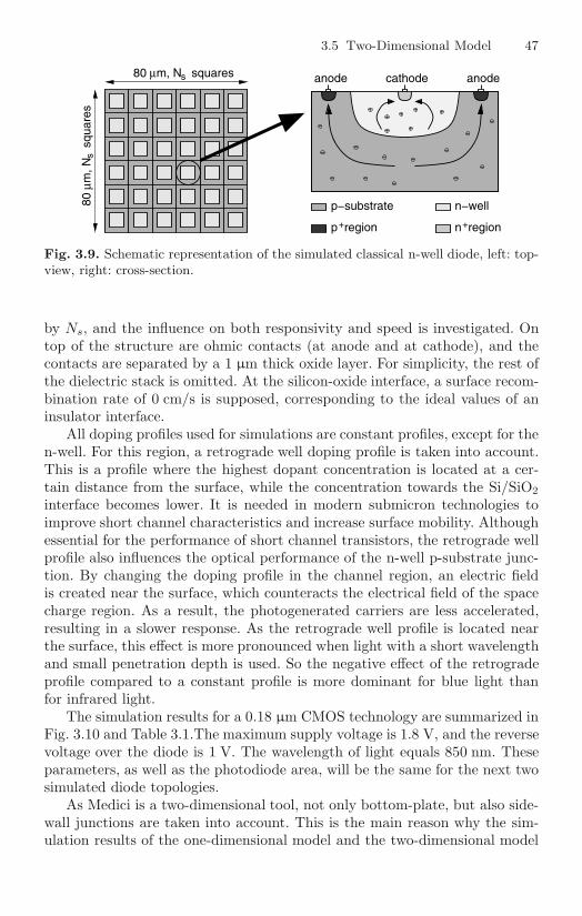
3.5 Two-Dimensional Model 47
n region+
80
m, N
sq
uare
sμ
anode cathode anode
n−well
p region+
p−substrate
μ80 m, N squaresss
Fig. 3.9. Schematic representation of the simulated classical n-well diode, left: top-view, right: cross-section.
by Ns, and the influence on both responsivity and speed is investigated. Ontop of the structure are ohmic contacts (at anode and at cathode), and thecontacts are separated by a 1 µm thick oxide layer. For simplicity, the rest ofthe dielectric stack is omitted. At the silicon-oxide interface, a surface recom-bination rate of 0 cm/s is supposed, corresponding to the ideal values of aninsulator interface.
All doping profiles used for simulations are constant profiles, except for then-well. For this region, a retrograde well doping profile is taken into account.This is a profile where the highest dopant concentration is located at a cer-tain distance from the surface, while the concentration towards the Si/SiO2
interface becomes lower. It is needed in modern submicron technologies toimprove short channel characteristics and increase surface mobility. Althoughessential for the performance of short channel transistors, the retrograde wellprofile also influences the optical performance of the n-well p-substrate junc-tion. By changing the doping profile in the channel region, an electric fieldis created near the surface, which counteracts the electrical field of the spacecharge region. As a result, the photogenerated carriers are less accelerated,resulting in a slower response. As the retrograde well profile is located nearthe surface, this effect is more pronounced when light with a short wavelengthand small penetration depth is used. So the negative effect of the retrogradeprofile compared to a constant profile is more dominant for blue light thanfor infrared light.
The simulation results for a 0.18 µm CMOS technology are summarized inFig. 3.10 and Table 3.1.The maximum supply voltage is 1.8 V, and the reversevoltage over the diode is 1 V. The wavelength of light equals 850 nm. Theseparameters, as well as the photodiode area, will be the same for the next twosimulated diode topologies.
As Medici is a two-dimensional tool, not only bottom-plate, but also side-wall junctions are taken into account. This is the main reason why the sim-ulation results of the one-dimensional model and the two-dimensional model

48 3 Standard CMOS Photodiodes
0 0.5 1 1.5 20
0.05
0.1
0.15
0.2
0.25
0.3
0.35
time (μs)
resp
onsi
vity
(A
/W)
Ns=4
Ns=6
Ns=8
Ns=10
Ns=12
Ns=14
(a)
106
107
108
109
1010
−40
−20
0
norm
. gai
n (d
B)
frequency (Hz)
106
107
108
109
1010
90
135
180
phas
e (d
egre
es)
frequency (Hz)
N =4sN =6sN =8s
N =10sN =12sN =14s
(b)
Fig. 3.10. Classical n-well diode simulation results: (a) responsivity, (b) normalizedintrinsic frequency characteristic. Ns corresponds to the number of squares per diodeside.
differ slightly in responsivity, but greatly in speed performance. Owing to theextra electric field regions of the side-wall junctions, the intrinsic photodi-ode speed becomes better in the two-dimensional model. The responsivity Rvaries between 0.33 A/W-0.29 A/W and turns out to be slightly dependenton the amount of squares. The higher Ns, the more useful area is taken bythe substrate contacts, the smaller R. The speed performance of the photo-diode is characterized by its intrinsic 3-dB bandwidth f3dB. It is mainly de-termined by the diffusing carriers in the substrate and independent of layouttopology. The simulated value equals 10 MHz. Leaving technology differencesaside, this value should be compared with the value found in the analyti-cal model: a 90 percent rise time of 260 ns for infrared light corresponds in

3.5 Two-Dimensional Model 49
n region+
80 m, N squaresμ80
m
, N
squa
res
μguard anode
cathode cathodeguard
n−well
+
p−substrate
p region
ss
Fig. 3.11. Schematic representation of the simulated p+ n-well diode with guard,left: top-view, right: cross-section.
a classical one-pole system to an intrinsic 3-dB bandwidth of 1.3 MHz. Thevalue of 10 MHz is considered to be more accurate, as the contribution of theside-wall junctions is included. These orders of magnitude correspond to thevalues reported by other authors (a 3-dB bandwidth of 4 MHz for a 0.25 µmtechnology [Gen01] and a ‘cut-off frequency’1 of 1 MHz for a 0.18 µm tech-nology [Rad05]). The low-frequency roll-off (< 50 Mz) is independent of Ns
and equals roughly 5 dB/decade. Note that this value is quite different fromthe slopes found in classical electronic systems, where one or multiple RC-constants determine a slope of 20 dB/decade, 40 dB/decade, etc. The systemunder study is not determined by some discrete R’s or C’s, but by the dis-tributed effect of carriers in n-well, depletion region and p-substrate.
3.5.2 P+ N-Well Diode with Guard
As already discussed in Section 3.4.2, eliminating the substrate carriers fromthe total signal would make the diode response a lot faster. This idea isimplemented in the p+ n-well diode with guard, shown schematically inFig. 3.11 [Woo98]. The basic diode structure is the same as the one of theclassical n-well diode, only now a p+ region is embedded in the n-well region.The amount of n-well regions is again given by Ns. The active junction de-tecting the signal is now the p+ n-well junction. The substrate contacts actas a guard to remove the substrate carriers. This photodiode is capable ofhigh-speed operation, at the expense of a smaller responsivity.
The simulation results regarding responsivity are shown in Fig 3.12(a).On top, for Ns = 4 to Ns = 14, the responsivity is shown if the p+ regionand p-substrate were placed parallel. These results are slightly smaller (dueto the extra interconnect overhead) compared to the classical n-well diode.The responsivity if the substrate contacts act as a guard, is approximately1 The cut-off frequency is defined in [Rad05] as the frequency at which the DC and
ac asymptotes of the total photodiode response cross.

50 3 Standard CMOS Photodiodes
0 0.5 1 1.5 20
0.05
0.1
0.15
0.2
0.25
0.3
time (μs)
resp
onsi
vity
(A
/W)
Ns=4
Ns=6
Ns=8
Ns=10
Ns=12
Ns=14
(a)
106
107
108
109
1010
−40
−20
0
norm
. gai
n (d
B)
frequency (Hz)
106
107
108
109
1010
−90
−45
0
phas
e (d
egre
es)
frequency (Hz)
N =4sN =6sN =8s
N =10sN =12sN =14s
(b)
Fig. 3.12. p+ n-well diode simulation results: (a) responsivity (upper curves:p+ n-well junction and p-substrate n-well junction in parallel, lower curves:p+ n-well junction with p-substrate guard), (b) normalized intrinsic frequency char-acteristic of the p+ n-well diode with guard. Ns corresponds to the number of squaresper diode side.
ten times smaller (0.023 A/W for Ns = 4 ), as shown in the same figure andsummarized in Table 3.1. On the other hand, as depicted in Fig. 3.12(b), theintrinsic 3-dB bandwidth is 100 times larger (1 GHz) and again independentof Ns. The frequency roll-off is also independent of Ns up to a few GHz. Theslope is slightly larger compared to the frequency slope of the classical n-welldiode: approximately 8 dB/decade instead of 5 dB/decade.
These results differ slightly from the one-dimensional analytical model,where red light instead of infrared light was applied. Probably the assumptionthat one half of the diffusing holes in the n-well is collected by the substrate

3.5 Two-Dimensional Model 51
contacts, and the other half by the p+ region contacts, is not correct whenthe two-dimensional problem is considered. The side-wall space charge re-gion of the n-well plays a non-negligible roll, because the n-well extents muchdeeper into the substrate than the p+ region. As a result, the major partof the n-well diffusion current is picked up by the side-wall space charge re-gion between n-well and p-substrate. Compared to the one-dimensional model,the responsivity in this model drops (from 0.09 A/W to ≤0.023 A/W). Thespeed improvement found in the one-dimensional model is only a factor of 10(Fig. 3.6(a) and Fig. 3.8(b): the rise time drops from 19 ns to 1.5 ns). Thetwo-dimensional model is more realistic, as the fast response of the side-walljunctions is included, although the speed improvement by a factor of 100might be rather optimistic.
3.5.3 Differential N-Well Diode
Another way to increase the diode bandwidth is to use a differential n-well diode. It is based on the same physical principles as the SML-detectorin [Roo00]. As depicted in Fig. 3.13, the differential n-well diode consists ofan alternating pattern of illuminated and dark junctions. The latter ones arecovered with metal to block the light. This diode also features substrate con-tacts alternating the junctions, again to minimize substrate resistance. Whenlight falls on this diode, carriers are generated below the illuminated junctionsand not below the dark junctions. The substrate carriers generated close toan illuminated junction will have a higher probability to reach this junctionthan to reach one of the neighboring dark junctions. Those generated deepin the substrate will require a long time to reach a junction and have moreor less equal probability to reach an illuminated or dark junction. If the re-sponse of the dark junctions is subtracted from the response of the illuminatedjunctions, a fast response is achieved as the influence of the slowly diffusingcarriers is cancelled.
Medici simulations have been performed using the amount of fingers, Nf ,as parameter. Rlight, theresponsivity of the illuminated junctions, is less thanone half of the responsivity of the classical n-well diode (see upper curves inFig. 3.14(a) and Table 3.1). This is because the same total area (80x80 µm2)is now taken by two diodes, the illuminated one and the dark one. The DC re-sponsivity of the differential signal (Rlight −Rdark) varies between 0.10 A/Wand 0.076 A/W. This is approximately one half of the responsivity of theilluminated junctions (see lower curves in Fig. 3.14(a) and Table 3.1), butstill more than 2 times larger than the responsivity of the p+ n-well diodewith guard. More fingers correspond to more interconnection overhead, anda slightly lower responsivity. The frequency characteristic of the differentialdiode is depicted in Fig 3.14(b). Its intrinsic 3-dB bandwidth ranges from1 GHz to more than 4 GHz, and does depend on the amount of fingers. Morefingers per diode means less distance for the diffusing carriers to bridge beforethey get detected, resulting in a faster response. These results are consistent

52 3 Standard CMOS Photodiodes
80 m, N fingers
80
mp region n region
������������������������������������������������������������������������������������
������������������������������������������������
������������
μp−substrate n−well
Illuminated junctionDark junction
++
μ
blocking metal
f
������������������������������������������������������������������������������������������������������������������������������������������������������������������������������������������������������������
������������������������������������������������������������������������������������������������������������������������������������������������������������������������������������������������������������
���������������������������������������������������������������������������������������������������������������������������������������������������������������������������������������������������������������������������������������������������������������
���������������������������������������������������������������������������������������������������������������������������������������������������������������������������������������������������������������������������������������������������������������
���������������������������������������������������������������������������������������������������������������������������������������������������������������������������������������������������������������������������������������������������������������
���������������������������������������������������������������������������������������������������������������������������������������������������������������������������������������������������������������������������������������������������������������
������������������������������������������������������������������������������������������������������������������������������������������������������������������������������������������������������������
������������������������������������������������������������������������������������������������������������������������������������������������������������������������������������������������������������
Fig. 3.13. Schematic representation of the simulated differential n-well diode, bot-tom: top-view, top: cross-section.
with the results found in [Gen01]. For the simulated frequencies of inter-est, there is no region of constant roll-off . The slope at each f3dB equals3 dB/decade, and rapidly rises to 10 dB/decade for frequencies above 10 GHz.These results show a trade-off between bandwidth and responsivity, and de-pending on the design goals, a proper choice of Nf has to be made.
3.5.4 Influence of Wavelength
Up till now, all photodiode simulations have been carried out for a wave-length of 850 nm. This wavelength corresponds to the wavelength used forshort-distance low-cost communication networks with multimode fiber. Forthe measurements described in Chapter 6 this wavelength will also be used.However, as described in Chapter 1, there are other low-cost applicationswhere monolithic CMOS implementations should be considered. First thereis the optical data storage, where three wavelengths are standardized: 780 nm(CD), 660 nm (DVD) and 405 nm (Blu-Ray Disc and HD-DVD). Second, notonly multimode fibers are used for short-distance communication, but alsoother kinds of fibers, working at a different optimal wavelength, might be ofinterest. For example, more and more cars are exploiting 650 nm plastic opti-cal fiber (POF) for their in-vehicle networks. As there is such a wide varietyof applications and standards, the influence of changing the wavelength isinvestigated.

3.5 Two-Dimensional Model 53
0 0.5 1 1.5 20
0.02
0.04
0.06
0.08
0.1
0.12
time (μs)
resp
onsi
vity
(A
/W)
Nf=18
Nf=22
Nf=26
Nf=30
Nf=34
(a)
106
107
108
109
1010−20
−10
0
norm
. gai
n (d
B)
frequency (Hz)
106
107
108
109
1010
90
135
180
phas
e (d
egre
es)
frequency (Hz)
N =18fN =22fN =26f
N =30fN =34f
(b)
Fig. 3.14. Differential n-well diode simulation results: (a) responsivity (uppercurves: Rlight, lower curves Rlight −Rdark), (b) normalized intrinsic frequency char-acteristic of the differential diode. Nf corresponds to the number of fingers.
Fig. 3.15 shows the simulation results for the classical n-well diode. Threedifferent cases are considered: A. infrared light (850 nm), B. red light (650 nm)and C. blue light (400 nm). The responsivity, depicted in Fig. 3.15(a), showsthe wavelength dependence of the energy per photon (3.1). The smaller thewavelength, the higher the energy per photon, the smaller the amount of pho-tons which can generate carriers and consequently the smaller the responsivity.Notice that also the penetration depth in combination with the carrier minor-ity lifetime determine responsivity. If the penetration depth is large (whichis true for large wavelengths), a lot of carriers will be generated deep intothe substrate, and will recombine before being detected. So although morephotons are present for the same amount of energy, less useful electrons will

54 3 Standard CMOS Photodiodes
Table 3.1. Simulated photodiode performance.
classical n-well diode p+ n-well diode with guard
Ns R (A/W) f3dB Ns R (A/W) f3dB
4 0.33
10 MHz
4 0.023
1 GHz
6 0.325 6 0.021
8 0.32 8 0.019
10 0.31 10 0.017
12 0.30 12 0.015
14 0.29 14 0.013
differential n-well diode
Nf Rlight (A/W) Rlight − Rdark (A/W) f3dB
18 0.10 0.052 1 GHz
22 0.094 0.046 1.5 GHz
26 0.088 0.042 2.2 GHz
30 0.083 0.038 3.1 GHz
34 0.076 0.034 4.4 GHz
be collected due to recombination. This explains why the responsivities of in-frared (850 nm) and red (650 nm) light are located close to each other, and caneven interchange when small simulation parameters are modified. The normal-ized frequency response for the three wavelengths is shown in Fig 3.15(b). Thesmaller the wavelength, the smaller the penetration depth, the higher the rela-tive contribution of the drift current, and thus the higher the 3-dB bandwidth.This results in a f3dB of 10 MHz for 850 nm light, 50 MHz for 650 nm light,and 75 MHz for 400 nm light. At lower frequencies, the slope is also wavelengthdependent. For 850 nm light, the roll-off equals 5 dB/decade, while the roll-off using smaller wavelengths is lower: 1.5 (dB/decade) for 650 nm light and1 dB/decade for 400 nm light. At higher frequencies (> 100 MHz) the curveshave equal slopes, but are shifted due to the higher bandwidth when shorterwavelengths are used. Around 100 MHz, the slope is steep, showing a roll-offof 15 dB/decade. Above 1 GHz, the steepness slows down and all curves havea slope of 5 dB/decade. At this frequency, the attenuation is larger than 15 dBfor all wavelengths.
The simulation results for the wavelength influence on the differential diodeare depicted in Fig. 3.16. For this diode topology, the responsivity (Rlight −Rdark) is the largest for 650 nm light, smaller for 400 nm light and the smallestfor 850 nm light. Rlight has the same dependence on wavelength as the classicaln-well diode described above. On the other hand, the smaller the wavelength,the smaller the penetration depth, the less diffusing carriers are generated,
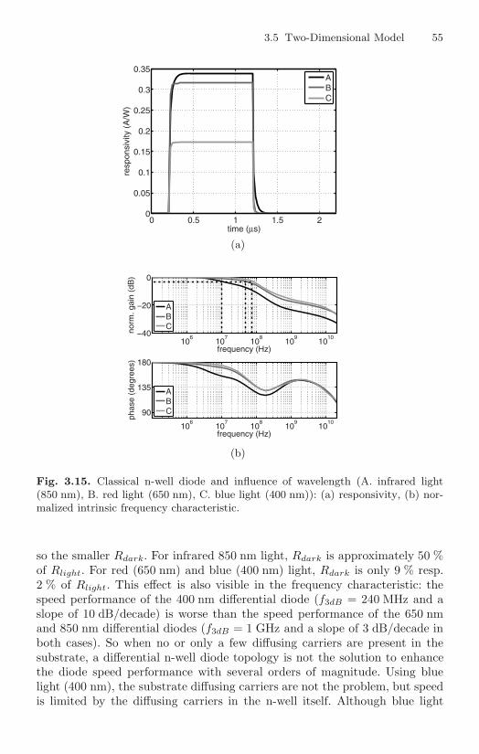
3.5 Two-Dimensional Model 55
0 0.5 1 1.5 20
0.05
0.1
0.15
0.2
0.25
0.3
0.35
time (μs)
resp
onsi
vity
(A
/W)
ABC
(a)
106
107
108
109
1010−40
−20
0
frequency (Hz)
norm
. gai
n (d
B)
ABC
106
107
108
109
1010
90
135
180
frequency (Hz)
phas
e (d
egre
es)
ABC
(b)
Fig. 3.15. Classical n-well diode and influence of wavelength (A. infrared light(850 nm), B. red light (650 nm), C. blue light (400 nm)): (a) responsivity, (b) nor-malized intrinsic frequency characteristic.
so the smaller Rdark. For infrared 850 nm light, Rdark is approximately 50 %of Rlight. For red (650 nm) and blue (400 nm) light, Rdark is only 9 % resp.2 % of Rlight. This effect is also visible in the frequency characteristic: thespeed performance of the 400 nm differential diode (f3dB = 240 MHz and aslope of 10 dB/decade) is worse than the speed performance of the 650 nmand 850 nm differential diodes (f3dB = 1 GHz and a slope of 3 dB/decade inboth cases). So when no or only a few diffusing carriers are present in thesubstrate, a differential n-well diode topology is not the solution to enhancethe diode speed performance with several orders of magnitude. Using bluelight (400 nm), the substrate diffusing carriers are not the problem, but speedis limited by the diffusing carriers in the n-well itself. Although blue light
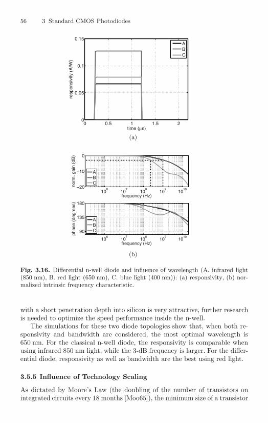
56 3 Standard CMOS Photodiodes
0 0.5 1 1.5 20
0.05
0.1
0.15
time (μs)
resp
onsi
vity
(A
/W)
ABC
(a)
106
107
108
109
1010−20
−10
0
frequency (Hz)
norm
. gai
n (d
B)
ABC
106
107
108
109
1010
90
135
180
frequency (Hz)
phas
e (d
egre
es)
ABC
(b)
Fig. 3.16. Differential n-well diode and influence of wavelength (A. infrared light(850 nm), B. red light (650 nm), C. blue light (400 nm)): (a) responsivity, (b) nor-malized intrinsic frequency characteristic.
with a short penetration depth into silicon is very attractive, further researchis needed to optimize the speed performance inside the n-well.
The simulations for these two diode topologies show that, when both re-sponsivity and bandwidth are considered, the most optimal wavelength is650 nm. For the classical n-well diode, the responsivity is comparable whenusing infrared 850 nm light, while the 3-dB frequency is larger. For the differ-ential diode, responsivity as well as bandwidth are the best using red light.
3.5.5 Influence of Technology Scaling
As dictated by Moore’s Law (the doubling of the number of transistors onintegrated circuits every 18 months [Moo65]), the minimum size of a transistor

3.5 Two-Dimensional Model 57
continually reduces. During the research period of this work, the most widelyused CMOS technology for analog design was the 0.18 µm CMOS technology.However, also 0.13 µm and 90 nm technologies were available. As 65 nm digitalCMOS technologies are emerging, the influence of technology scaling on thediode performance should be considered.
When technology size decreases, doping concentration levels increase tocounteract the effect of scaling on transistor characteristics (VT , leakage cur-rents, etc.). Also, the available power supply drops to keep the electrical fieldwithin limits. As a result, the width of space charge regions (eg. for the n-wellp-substrate junction given by (3.22)) decreases. This will result in a smallercontribution of the drift current (3.21) to the total current. Fig. 3.17 showsthe influence of downscaling on the optical performance of the classical n-welldiode and the differential n-well diode. A 0.18 µm CMOS technology is com-pared with a 0.13 µm CMOS technology. Both responsivity and 3-dB band-width of the diodes become slightly worse when technology scales down. Thelow-frequency roll-off of the classical diode is 5 dB/decade for both technolo-gies. The differential n-well diode does show some technology dependence: theslope is slightly steeper around f3dB for the smaller technology: 5 dB/decadecompared to 3 dB/decade.
Notice that the simulations for the differential diode were carried out fora fixed amount of fingers Nf . When minimal sizes are reducing, smaller n-well fingers can be taken, resulting in a faster detector response. The effectof having smaller fingers is actually presented in Fig. 3.14(b), but only forthe 0.18 µm technology. Moreover, as technology dimensions shrink, the areaoverhead needed for n-well and substrate contacts will become less. This willresult in less area covered with light-blocking metal, and more efficient areataken by photo-sensitive junctions. So despite all the drawbacks, technologyscaling might have some advantages for integrated differential photodiodes.
Finally, Table 3.2 draws attention to another important parameter whichmodifies as a result of technology changes, namely the junction capacitance.As will become clear in Section 4.3.1, its value is inversely proportional tothe bandwidth of the transimpedance amplifier, and thus greatly influencesthe speed of the overall receiver. Due to doping concentration modifications(resulting in smaller depletion widths), the zero bias junction capacitancebecomes higher. Especially the increase of the side-wall capacitance is re-markable: more than a factor of ten per unit meter. Table 3.2 also comparesthe total capacitance of the classical n-well diode and the differential n-welldiode implemented in two different technologies and reversely biased at onehalf of the respectively available power supply (1.8 V versus 1.2 V). For thedifferential diode, the capacitance of the illuminated junctions (equal to thecapacitance of the dark junctions) should be considered, as the currents ofthese junctions are amplified separately. This value is approximately one halfof the capacitance of the classical n-well diode, which is consistent with theoccupied diode area. A technology change from 0.18 µm CMOS to 0.13 µmCMOS means roughly a 4 times increase of the n-well p-substrate junction

58 3 Standard CMOS Photodiodes
0 0.5 1 1.5 20
0.05
0.1
0.15
0.2
0.25
0.3
0.35
time (μs)
resp
onsi
vity
(A
/W)
ABCD
(a)
106
107
108
109
1010−20
−10
0
frequency (Hz)
norm
. gai
n (d
B)
ABCD
106
107
108
109
1010
90
135
180
frequency (Hz)
phas
e (d
egre
es)
ABCD
(b)
Fig. 3.17. Influence of technology scaling (A. classical n-well diode 0.18 µm, B. clas-sical n-well diode 0.13 µm, C. differential n-well diode 0.18 µm, D. differential n-welldiode 0.13 µm): (a) responsivity, (b) normalized intrinsic frequency characteristic.
capacitance. These values have to be taken into account during the tran-simpedance amplifier design.
3.6 Conclusions
This chapter was completely devoted to one single device: the photodiode.It has an important function in the optical receiver, as it is the interfacebetween the optical and the electrical domain. Its speed and responsivity areof uttermost importance for the performance of the complete receiver chain.
To understand the opto-electrical mechanisms, some definitions have beenintroduced first. Next, to illustrate the feasibility of integrated silicon photo-

3.6 Conclusions 59
Table 3.2. Junction capacitance and technology scaling.
0.18 µm CMOS 0.13 µm CMOS
Zero bias area junction capacitance 1.07 · 10−4 F/m2 2.17 · 10−4 F/m2
Zero bias side-wall junction capacitance 2.4 · 10−11 F/m 2.7 · 10−10 F/m
total capacitance428 f F 1.5 pF
classical n-well diode (Ns = 10)
total capacitance illuminated junctions210 f F 875 f F
differential n-well diode (Nf = 26)
detectors, some published BiCMOS, SOI and CMOS implementations havebeen discussed. The advantage of CMOS over the other technologies is alower cost, making it the chosen technology for low-cost, high-volume massapplications.
The light detection principles and carrier transport mechanisms involvedin a pn-junction have been described both qualitatively and quantitativelyusing semiconductor physics. This one-dimensional model shows that the n-well p-substrate junction can be used to detect light, but the rise time for redlight is only 19 ns. The speed can be enhanced using the p+ n-well junction,which is shielded from the diffusing substrate carriers by the n-well p-substratejunction. The improved rise time of 1.5 ns comes at the expense of a lowerresponsivity: 0.09 A/W compared to 0.32 A/W.
A two-dimensional model has been developed to include the non-negligibleeffect of side-wall junction capacitances. Also the retrograde well doping pro-file has been taken into account. Depending on the amount of substrate con-tacts, the classical n-well diode has a responsivity ranging from 0.29 A/W to0.33 A/W. The speed is mainly limited by the diffusing carriers in the sub-strate, and independent of the n-well layout topology. The photodiode 3dB-bandwidth equals 10 MHz, while the low-frequency roll-off is 5 dB/decade.
Two diode topologies to enhance the speed performance have been inves-tigated using this two-dimensional model: the p+ n-well diode with guard andthe differential n-well diode. For the first topology, speed is again not muchinfluenced by the amount of n-well squares, and the diode 3-dB bandwidthequals 1 GHz. For the latter diode, the amount of n-well fingers does affectbandwidth, which varies from 1 GHz (18 fingers) to 4.4 GHz (34 fingers). Thedifferential diode is not only capable of higher bitrates, also the responsivityis better: for a simulated bandwidth of 1 GHz, the responsivity is 0.052 A/Wfor the differential diode versus maximum 0.023 A/W for the p+ n-well diodewith guard.
The two-dimensional results discussed above all reflect the photodiodeperformance for 850 nm light, used in short-distance communication networks.Because there exists a lot of low-cost applications using shorter wavelengths,the performance of the classical and differential diode has been studied usingred (650 nm) and blue light (400 nm) . The light wavelength does influence

60 3 Standard CMOS Photodiodes
the optical performance, and red light turns out to be the most “optimal”wavelength concerning speed and responsivity. When blue light is used, thedifferential diode topology becomes pointless, as there are no diffusing carriersin the substrate which have to be compensated for.
As Moore’s Law is still valid in the silicon nano-scaled technology, the con-sequences of the transition from a 0.18 µm to a 0.13 µm technology have beendiscussed. Due to higher doping levels and smaller supply voltages, the widthof the space charge region becomes smaller, resulting in photodiodes witha slightly smaller responsivity, a lower 3-dB bandwidth and a higher capaci-tance value. The latter result will directly have impact on the transimpedanceamplifier design.
Finally, an important conclusion concerning all the device simulations inthis chapter is that there exists a trade-off between responsivity and speed.Depending on the system requirements and consequently the diode specifica-tions, a proper design choice has to be made.

4
Transimpedance Amplifier Design
4.1 Introduction
The transimpedance amplifier (TIA) is without a doubt the most criticalbuilding block of the optical receiver. It converts the current generated by thephotodiode into an output voltage. The design of this block involves manytrade-offs between noise, bandwidth, gain and stability. This chapter tries toreveal all subtleties and challenges encountered during the design of low-noisehigh-bandwidth TIAs.
A summary of the TIA specifications regarding transimpedance gain,bandwidth, noise and overload currents is given in Section 4.2. Section 4.3tackles the design of a TIA with shunt-shunt feedback. Design equations arederived for the transimpedance gain, bandwidth, open-loop gain, loop gainand the noise performance. Implementations published in open literature arediscussed in Section 4.4. Two main topologies are distinguished: the TIA withcommon-source input stage and the TIA with regulated cascode input stage.Also some interesting work presented at ISSCC is described. Finally, the de-signs of three different TIAs, of which two are implemented in a 0.18 µmCMOS and one in a 90 nm CMOS technology, are explained more thoroughlyin Section 4.5. These case studies clearly demonstrate the compromises to bemade during the design of low-noise high-speed TIAs.
4.2 Performance Requirements
This section presents the main performance requirements for a TIA: hightransimpedance gain, high bandwidth, low noise and high overload current.
Transimpedance Gain
The transimpedance gain of the TIA, ZTIA, is defined as the ratio of thesmall-signal output voltage to the small-signal input current:
61

62 4 Transimpedance Amplifier Design
ZTIA =vout
iin= |ZTIA(f)|ejθ(f). (4.1)
The higher this value, the more output signal is produced for a given inputsignal. The transimpedance gain is specified either in units of Ω or dBΩ.The value dBΩ is calculated as 20 · log10(ZTIA/Ω). The transimpedance gainis a complex quantity, with frequency-dependent magnitude |ZTIA(f)| andfrequency-dependent phase shift θ(f). The transimpedance gain at low fre-quencies is usually flat, and represented by ZTIA,0.
The first reason for having a TIA with high gain is to create a signal withan amplitude large enough to drive the post-amplifier (PA). But there is anadditional reason which might be even more important: noise. As the TIA isthe first stage in the optical receiver (Fig. 2.1), the noise of the next stageslike the PA will be suppressed by the TIA gain. So a lower transimpedancegain (for example to obtain a higher bandwidth (4.11)) cannot simply beexchanged for a larger post-amplification. The total gain remains constant,but the total input-referred noise of the receiver will increase.
Bandwidth
The upper frequency at which |ZTIA(f)| (4.1) has dropped 3 dB below its DCvalue, is defined as the TIA bandwidth, BWTIA.
As discussed in Section 2.5, a limited bandwidth causes ISI and degradesthe opening of the eye diagram. To receive data with a certain bitrate Rb,the bandwidth must be as high as possible to minimize the ISI. But on theother hand, Section 4.3.3 will demonstrate that a large bandwidth increasesthe noise picked up by the TIA. As a compromise between noise and ISI, aTIA bandwidth equal to 0.7Rb is commonly used [Raz03, Sac05].
Noise
The input-referred current noise is one of the most critical TIA parameters.Often the noise of the TIA dominates all other noise sources and thereforedetermines the sensitivity of the receiver. The equivalent input-referred noisecurrent is the current source that, together with the ideal noiseless TIA, re-produces the output noise of the actual noisy TIA. As stated before in Sec-tion 2.4.2, it is a fictitious quantity that cannot be observed in the actualcircuit.
To determine the input-referred noise current, the noise power spectraldensity at the output for each noise source is calculated first. Typical noisesources are transistors, resistors and diodes. Assuming these sources are notcorrelated, they add up to form the total output noise power spectral density.The power spectral density of the input-referred noise current, di2n,TIA, canthen be found by taking the frequency-dependent transimpedance gain intoaccount:

4.3 Design of the Shunt-Shunt Feedback TIA 63
di2n,TIA =dv2
n,TIA
|ZTIA(f)|2 . (4.2)
The input-referred rms noise current, in,rms (2.7), also called the total inte-grated input-referred noise current of the TIA, in,TIA, is determined by divid-ing the rms output noise voltage by the DC value of the transimpedance gain.The rms output noise voltage is obtained by integrating the output-referrednoise spectrum and taking the square root.
in,TIA =1
ZTIA,0
√∫ ∞
0
dv2n,TIAdf. (4.3)
Note that this definition is different from integrating the input-referred noisecurrent to a certain bandwidth. For analytical calculations, the integration hasto be carried out to infinity. For simulations and measurements, a few timesthe bandwidth BWTIA, or simply the bandwidth (for higher order TIAs witha steep roll-off) is taken as upper limit.
For completeness, the definition of noise bandwidth BWn is repeated here.It is the bandwidth, multiplied by the DC value of the power spectral noisedensity, which gives the same result as the integration of the power spectralnoise density to infinity. For a first order circuit, BWn equals π
2 times the3-dB bandwidth [San06]. For a third order circuit with a steeper slope, thenoise bandwidth and the 3-dB bandwidth nearly coincide.
Overload Current
A TIA may receive large signal currents, for example when the distance be-tween transmitter and receiver is very short and the photodetector has a highresponsivity. As the input level increases, the TIA will introduce nonlinearitiesin the signal. Due to the binary nature of transmitted data, some nonlinearitycan be tolerated. However, too much nonlinearities may corrupt the signallevels and/or distort the zero crossings, increasing the BER. Naturally, thishas to be avoided.
Following the simulations of Chapter 3, the responsivity of integratedCMOS diodes is rather low, because the standard silicon technology is notoptimal for optical applications. So even for large optical signals, the currentsat the input will remain below the overload current.
4.3 Design of the Shunt-Shunt Feedback TIA
The TIA topology used in this work is the so-called shunt-shunt feedback TIA.A negative feedback network senses the voltage at the output and returns aproportional current to the input. This type of feedback has the advantagethat it lowers both the input and output impedance. As a result, the closed-loop bandwidth is increased by the loop gain. In this section, the main designequations for the shunt-shunt feedback TIA are derived.

64 4 Transimpedance Amplifier Design
Cdio Cin
Rout
CinCdio
C inT
Rout
R f
voutvin
vin
R f
CCIout next
PD
dio
TIA
nin nout
(a)
(b)
0A
noutnin
CoutT
Cout nextC−A0idio
Fig. 4.1. The shunt-shunt feedback TIA: (a) general schematic, (b) small-signalequivalent circuit.
4.3.1 Transimpedance Gain and Bandwidth
Fig. 4.1(a) shows a general schematic of the shunt-shunt feedback TIA. Thephotodiode is represented by the current source Idio in parallel with the junc-tion capacitance Cdio. The TIA consists of a voltage amplifier with DC gainA0 and feedback resistance Rf . The input capacitance Cin and output capac-itance Cout are determined by the sizes of the transistors that constitute thevoltage amplifier. Cnext is the input capacitance of the next stage. Rout is theTIA output resistance and is usually much smaller than Rf .
The analysis of the small-signal equivalent circuit, depicted in Fig. 4.1(b),results in following transimpedance gain:
ZTIA =vout
idio=
ZTIA,0
s2 Rf RoutCinT CoutT
A0+1 + s(
(Rf+Rout)CinT
A0+1 + RoutCoutT
A0+1
)+ 1
,
(4.4)with:
ZTIA,0 =RfA0
A0 + 1− Rout
A0 + 1≈ Rf , (4.5)
4.3 Design of the Shunt-Shunt Feedback TIA 65
CinT = Cdio + Cin, (4.6)CoutT = Cout + Cnext. (4.7)
According to (4.5), the transimpedance gain at low frequencies equals Rf forlarge values of A0 and small values of Rout.
To find the bandwidth of (4.4), two separate cases are considered. First,suppose the second pole of the TIA has a much higher magnitude than thefirst pole. Taking into account following approximations:
A0 + 1 ≈ A0, (4.8)Rout � Rf , (4.9)
RoutCoutT � RfCinT , (4.10)
the well-known expression for the TIA bandwidth BWTIA can be found:
BWTIA =A0
2πRfCinT. (4.11)
The dominant pole, which determines the bandwidth in this case, is locatedat the input node nin. Due to the feedback loop, the resistance at this node isdivided by the loop gain, which results in a factor A0 increase of bandwidth.Therefore, A0 has to be maximized during the design process. Other factorsthat influence bandwidth are the feedback resistor Rf and the total input ca-pacitance CinT . Rf usually cannot be made too small for gain (4.5) and noiseconsiderations (4.36). CinT consists of two parts: Cdio, determined by the pho-todiode topology, and Cin, which increases for larger transistor dimensions.This expression for the bandwidth reveals two important conclusions:
• As the photodiode junction capacitance directly appears in the denomina-tor of (4.11), a photodiode-TIA co-design is mandatory.
• A design aiming for high bandwidth implies an optimization of the voltagegain A0.
The non-dominant pole is located at the output node nout. It coincides withthe bandwidth BWV A of the voltage amplifier, which has only one pole in thesimplified model of Fig. 4.1.
fnd,TIA = BWV A =1
2πRoutCout. (4.12)
However, the two poles of a second-order system can seldom be treatedas two real poles. Mostly, they will be part of a complex conjugated pair.In basic control theory, the denominator of a second-order system is writtenas [Dor98]: ( s
ωn
)2
+ 2ζ( s
ωn
)+ 1, (4.13)
where ζ is the dimensionless damping ratio and ωn is the natural pulsation ofthe system. When ζ = 1, the system is critically damped. Complex conjugated

66 4 Transimpedance Amplifier Design
poles occur when ζ < 1. The relation between 3-dB bandwidth ω3dB, naturalpulsation ωn and damping ratio ζ can be calculated by setting the magnitudeof (4.13) equal to 2/
√2:
ω3dB
ωn= (1 − 2ζ2) +
√2√
2ζ4 − 2ζ2 + 1. (4.14)
A smaller ζ will result in a larger 3-dB bandwidth, but also a higher overshootin the time domain and a larger resonance peaking in the frequency domain.This causes degradation of the high and low levels and jitter in the eye dia-gram, despite the large bandwidth. In [Dor98] the percent overshoot P.O. isdefined by:
P.O. = 100e−ζπ/√
1−ζ2. (4.15)
Setting ζ equal to√
2/2 is an attractive solution. The percent overshoot is only4 %, while the 3-dB bandwidth equals ωn. It also generates a system with amaximally flat frequency response, which corresponds to a Butterworth filter.This way, a compromise is found between bandwidth and overshoot, leadingto a high-quality eye diagram.
Equating (4.13) with the denominator of (4.4) gives following results forthe natural pulsation and damping ratio of the second-order TIA depicted inFig. 4.1:
ωn =
√A0 + 1
RfRoutCinT CoutT, (4.16)
ζ =12
Rf CinT
RoutCoutT+ 1√
(A0 + 1) Rf CinT
RoutCoutT
. (4.17)
For sufficiently large gain A0, the last equation can be rewritten as:
1RoutCoutT
= 4ζ2 A0
RfCinT. (4.18)
This is the condition at the input node nin and output node nout of Fig. 4.1which has to be fulfilled to design a TIA with a certain damping ratio ζ. Com-bining (4.18) and (4.16), the corresponding natural pulsation can be found.More interesting is the 3dB-bandwidth, which can be calculated using (4.14).The results for some typical values of ζ are summarized in Table 4.1.
Comparing the fourth column of Table 4.1 with the earlier derived expres-sion for the TIA bandwidth, (4.11), an increase in bandwidth is noticed. Thesystem under study is unchanged, only the basic assumptions for the handcalculations are different. In the case of (4.11), the TIA has two well-separatedreal poles while in the other case, the poles are complex conjugates. Due tothese complex poles, the resulting 3dB-bandwidth is larger, but some over-shoot will occur in the eye diagram. However, this is tolerable as long as the

4.3 Design of the Shunt-Shunt Feedback TIA 67
Table 4.1. Design equations for the second-order TIA of Fig. 4.1.
ζ Condition (4.18) ωn (4.16) ω3dB (4.14) P.O. (4.15) P.M. (4.27)
12
1RoutCoutT
= A0Rf CinT
A0Rf CinT
1.6A0Rf CinT
16 % 45◦
√2
21
RoutCoutT= 2A0
Rf CinT
√2A0
Rf CinT
√2A0
Rf CinT4 % 63◦
√3
21
RoutCoutT= 3A0
Rf CinT
√3A0
Rf CinT
1.07A0Rf CinT
0.4 % 72◦
damping ratio is high enough and no ringing occurs. The smaller ζ, the higherthe bandwidth, but the more overshoot and ringing. Also the phase margindecreases with ζ. An expression for the phase margin (P.M.) will be derived inthe next subsection. Most important is that the main conclusions of (4.11) arestill valid: the TIA bandwidth BWTIA is inversely proportional to the inputcapacitance CinT (which contains the photodiode capacitance Cdio), inverselyproportional to the feedback resistor Rf , and directly proportional to the DCgain A0 of the voltage amplifier. Note also that for ζ =
√3/2, the expression
for the bandwidth almost equals (4.11). The first two designs discussed inSection 4.5 will use a rather safe phase margin of at least 72◦. The last designwill allow more overshoot in exchange for a higher bandwidth, so ζ will bemore around
√2/2. This overshoot can be tolerated, as the TIA is followed
by a limiting amplifier, which will be discussed in Chapter 5.To compare the performance of different TIAs, a parameter which takes
into account several of its characteristics is needed. In analogy with the gain-bandwidth product GBW of voltage amplifiers [San06], the transimpedance-bandwidth product ZBW is used to evaluate the TIA performance. It isdefined by the product of its transimpedance gain ZTIA,0 and its 3-dB band-width BWTIA:
ZBW = ZTIA,0 ·BWTIA ≈ A0
2πCinT. (4.19)
The transimpedance-bandwidth is independent of the feedback resistor Rf .To some extent, transimpedance gain can simply be exchanged for bandwidthand vice versa, by changing the value of Rf . The only limitation is that thedamping ratio has to be high enough, or equivalently, that there needs to besufficient phase margin. (Table 4.1). The transimpedance-bandwidth ZBW(4.19) again emphasizes the importance of the voltage gain A0. As the totalinput capacitance is largely determined by the photodiode capacitance, whoseparameters are dictated by technology rules and fiber size, the only way tooptimize ZBW is by maximizing A0.

68 4 Transimpedance Amplifier Design
vinR fR f
R f
vout
inTC −A0
vin
dioi
RoutRout outTC
RfRf inTC
−Rf
1+s−A0
outT
out
+s
1
v
vindioi vout
TIAG
Rf
1
CRf
vin
Rout
(a)
noutnin
(b)
1+
Fig. 4.2. TIA representations to determine open-loop gain and loop gain: (a) Coatestransformation of Fig. 4.1(b), (b) block diagram.
4.3.2 Open-Loop Gain and Loop Gain
Another way of looking at the TIA with shunt-shunt feedback, is depictedin Fig. 4.2(a). The feedback resistor Rf between nodes nin and nout is re-placed by its Coates transformation: resistor Rf and voltage-controlled currentsource vout/Rf between node nin and ground; and resistor Rf and voltage-controlled current source vin/Rf between node nout and ground. Startingfrom this equivalent circuit, the block diagram of Fig. 4.2(b) can be derived.It represents the feedback system by its open-loop gain GTIA and loop gainGHTIA.
In the block diagram of Fig. 4.2(b), the feedforward voltage controlledcurrent source vin/Rf has been neglected. This is allowed if ARf � Rout,which is almost always true. The expression for the open-loop gain GTIA isthen given by:
GTIA =A0Rf
(1 + sRfCinT )(1 + Rout
Rf+ sRoutCoutT )
. (4.20)
If it also can be assumed that Rf � Rout, the open-loop gain further reducesto:
GTIA =A0Rf
(1 + sRfCinT )(1 + sRoutCoutT ). (4.21)
The loop gain GHTIA equals the open-loop gain GTIA times the feedbackfactor 1/Rf , or:

4.3 Design of the Shunt-Shunt Feedback TIA 69
GHTIA =A0
(1 + sRfCinT )(1 + sRoutCoutT ). (4.22)
The phase margin is often used in basic control theory to study the stabilityof feedback systems [Dor98]. It is the amount of extra phase shift of the loopgain (GHTIA) at unity magnitude (or 0 dB) that will result in a phase angleof 180◦. To derive an expression for the phase margin, it is assumed that thepoles of (4.22) are real and differ a lot in magnitude. So the dominant polefd,GH and non-dominant pole fnd,GH of the loop gain GHTIA can readily befound:
fd,GH =1
2πRfCinT, (4.23)
fnd,GH =1
2πRoutCoutT. (4.24)
Note that the latter is also the pole which determines the bandwidth of thevoltage amplifier, BWV A (4.12). The unity-gain frequency of the loop gainf0dB,GH is given by:
f0dB,GH =A0
2πRfCinT, (4.25)
assuming fd,GH � f0dB,GH � fnd,GH . Under the same condition, the phaseangle at this frequency equals:
θ(f0dB,GH) = −(π
2+ arctan
(f0dB,GH
fnd,GH
). (4.26)
This results in the expression for the phase margin P.M.:
P.M. =π
2− arctan
(f0dB,GH
fnd,GH
)= arctan
( fnd,GH
f0dB,GH
). (4.27)
For instance, if fnd,GH = 3 · f0dB,GH, the phase margin equals 72◦. Otherexamples for smaller ratios are given in Table 4.1. Note however that theseare hand calculations and that the expression for the P.M. approaches realityonly if fd,GH � f0dB,GH � fnd,GH . For the other equations in Table 4.1, therequirements regarding pole location are less stringent.
The expressions derived so far are valid for the voltage amplifier modeldepicted in Fig. 4.1, which has only one dominant pole at the output. If thevoltage amplifier consists for example of three identical amplifying stages,three more or less identical poles fnd,GH are present. The loop gain can nowbe approximated by:
GHTIA =A0
(1 + sRfCinT )(1 + sfnd,GH
)3, (4.28)
and the phase margin:

70 4 Transimpedance Amplifier Design
P.M. =π
2− 3 ·arctan
(f0dB,GH
fnd,GH
), (4.29)
with f0dB,GH given by (4.25). To achieve the same phase-margin, the ratioof f0dB,GH to fnd,GH has to be approximately three times smaller than theratio in (4.27). So assuming the same f0dB,GH , the non-dominant pole of theloop-gain, which coincides with the bandwidth of the voltage amplifier, hasto be three times higher in frequency for a three-stage amplifier compared toa single-stage amplifier.
A good reason for choosing a multiple-stage approach would be to increasethe voltage amplifier’s gain A0. This way, the bandwidth BWTIA is enlarged,or for the same bandwidth, the feedback resistance Rf can be larger (4.11).As will become clear in Section 4.3.3, a larger Rf leads to a better TIA noiseperformance and thus a better receiver sensitivity. However, due to stabil-ity requirement (4.29), the voltage gain of a three-stage amplifier is limitedby the ratio of the bandwidth of the TIA (BWTIA) and the fT of a cer-tain technology. In [Ing04] it is demonstrated that, when BWTIA ≈ 0.1fT orlarger, the maximal achievable gain of a single stage voltage amplifier is largerthan the maximal achievable gain of a three-stage voltage amplifier. Appli-cations demanding a high bandwidth compared to the technology’s fT haveto implement a single-stage amplifier rather than a three-stage amplifier, asthere is simply no room for placing the extra poles which are introduced in amultiple-stage approach. However, for frequencies 20 to 30 times below fT , amultiple-stage amplifier is the best design choice.
4.3.3 Noise
The noise sources of the shunt-shunt feedback TIA are added to the generalschematic in Fig. 4.3. Two TIA noise sources can be distinguished: the noisefrom the feedback resistor and the noise from the voltage amplifier. The thirdnoise source stems from the noise generated by the photodiode.
Noise Densities of the Three Noise Sources
The thermal noise of the resistor is modeled by a current noise source di2Rf inparallel:
di2Rf =4kT
Rfdf. (4.30)
The noise current power is proportional to the absolute temperature in Kelvin,and inversely proportional to the value of the feedback resistor Rf . It is whitenoise, as it does not change with frequency.
The noise of the voltage amplifier is represented by the noise of an equiv-alent input transistor Mx with equivalent transconductance gmx. In most de-signs, where the input stage features large gain, the equivalent transistor Mx
simply corresponds to the input transistor of the voltage amplifier. For a MOS

4.3 Design of the Shunt-Shunt Feedback TIA 71
inCCdio
outR
Cout Cnext
fR
2diRf
dio2di
2
xM
Idio
di
x
noutnin
M
0A
Fig. 4.3. The shunt-shunt feedback TIA with the most important noise sources.
transistor, the classical thermal channel noise di2Mx is still the most importantnoise source. It is given by:
di2Mx = 4kTγgmxdf, (4.31)
where γ is the excess noise factor. This noise current power is also whiteand proportional to the absolute temperature and to the transconductancegmx. For long-channel devices, γ = 2/3. In short-channel devices the effectivetemperature of the carriers is significantly larger due to the high electric fieldin the channel and γ can be as high as 2 or 3. The pMOS transistor usuallyexhibits lower γ values than its nMOS counterpart.
Finally, the last noise source is the noise from the photodiode di2dio. Mostly,it consists only of shot noise, which is given by:
di2dio = 2qIdiodf. (4.32)
The shot noise current power is also white, and proportional to the currentflowing through the junction. This noise power is data-dependent: when aphotodiode receives a zero, no light power is received, and the current Idio is(almost) zero. When a one is received, the generated noise depends on the re-ceived light power and the photodiode responsivity. As the noise current varieswith time, it is called non-stationary. However, in most cases, the photodiodeshot noise can be neglected.
Output Noise Spectral Density and Input-ReferredNoise Spectral Density
The power spectral density of the output noise voltage is given by the noisecurrent power of each noise source, multiplied by the square of its transferfunction to the output.

72 4 Transimpedance Amplifier Design
dv2n,TIA =
di2dioZ2TIA,0∣∣∣s2 Rf RoutCinT CoutT
A0+1 + s(
(Rf+Rout)CinT
A0+1 + RoutCoutT
A0+1
)+ 1
∣∣∣2
+di2Rf
∣∣∣Rf A0A0+1
∣∣∣2∣∣∣1 + sRoutCinT
A0
∣∣∣2
∣∣∣s2 Rf RoutCinT CoutT
A0+1 + s(
(Rf+Rout)CinT
A0+1 + RoutCoutT
A0+1
)+ 1
∣∣∣2
+di2Mx
∣∣∣Rout
A0
∣∣∣2∣∣∣1 + sRfCinT
∣∣∣2
∣∣∣s2 Rf RoutCinT CoutT
A0+1 + s(
(Rf+Rout)CinT
A0+1 + RoutCoutT
A0+1
)+ 1
∣∣∣2 .
(4.33)
This expression can be simplified using following assumptions:
• The shot noise of the photodiode is negligible small compared to the othernoise sources.
• A0 + 1 ≈ A0.• The zero A0
2πRoutCinTis located at a frequency beyond the frequency range
of interest. This corresponds to neglecting the feedforward current of Rf ,injected by its noise source in node nout.
• Following the one-transistor equivalent of the voltage amplifier, gmxRout =A0.
The resulting expression for the output noise spectral density is:
dv2n,TIA =
4kTRfdf∣∣∣s2 Rf RoutCinT CoutT
A0+1 + s(
(Rf+Rout)CinT
A0+1 + RoutCoutT
A0+1
)+ 1
∣∣∣2
+4kTγdf
gmx
∣∣∣1 + sRfCinT
∣∣∣2
∣∣∣s2 Rf RoutCinT CoutT
A0+1 + s(
(Rf+Rout)CinT
A0+1 + RoutCoutT
A0+1
)+ 1
∣∣∣2 .
(4.34)
This expression is plotted versus log(f) in Fig. 4.4(a). At low frequencies,the noise is dominated by the feedback resistor’s thermal noise. At higherfrequencies and for a sufficient high gain A0, the amplifier noise may becomedominant. Note that the integration of the power spectral density in this casewill lead to an integrated output noise voltage which is dominated by thenoise of the amplifier. The representation in Fig. 4.4(a) may suggest some-thing else, but it is misleading due to the logarithmic frequency axis whichoveremphasizes the integrated low-frequency noise.
In a design aiming primarily for large bandwidth, the dominant noisesource might be the feedback resistor and not the amplifier. This is the casewhen the zero and poles of (4.34) are located close to each other, which isusually true for high BWTIA/fT ratios. As the bandwidth is comparable to

4.3 Design of the Shunt-Shunt Feedback TIA 73
BWTIA fnd,TIA
amplifierR
total
Rf4kT
gmx
4kTγ
gmx
4kTγA20
Rf2π CinT
1
n,TIA2
f (Hz)
fdv(dB/Hz)
(a)
amplifierR
total
Rf
Rfgmx
4kTγ2
n,TIA2di
Rf2π CinT
1
4kT
f(dB/Hz)
f (Hz)
(b)
Fig. 4.4. Power spectral densities of: (a) TIA output noise, (b) TIA input-referrednoise.
fT , there is not much headroom left to place the other poles. An additionaladvantage is that complex conjugated poles increase the bandwidth, as dis-cussed in Section 4.3.1. Moreover, the noise generated by the feedback resistoris quite large, as the TIA bandwidth is inversely proportional to its resistancevalue. This value is a few orders of magnitude smaller than in traditional de-signs, where a bandwidth of a few megahertz is sufficient. Finally, also thevoltage gain A0 cannot be very large as too much loop gain can cause stabil-ity problems. As a result, the maximum value for the amplifier output noisepower spectral density depicted in Fig. 4.4(a) and given by:
4kTγ
gmxA2
0, (4.35)
will not be reached and the actual maximum will stay below 4kTRf . Examplesof different output noise spectral densities will be discussed in Section 4.5.
To compare the output voltage noise with the input photodiode current,the output noise is referred to the input. According to (4.2), the power spectraldensity of the input-referred current noise is given by the division of (4.34) bythe square of (4.4).
di2n,TIA =4kT
Rfdf +
4kTγdf
gmxR2f
∣∣∣1 + sRfCinT
∣∣∣2
. (4.36)
This expression is plotted versus frequency in Fig. 4.4(b). The first term iscaused by the feedback resistor Rf . It is frequency independent and equalto the thermal noise of Rf (4.30). Neglecting the feedforward noise current,only the feedback current at the input remains which directly adds up with thephotodiode current. The larger Rf , the smaller this noise, but also the smallerthe TIA bandwidth BWTIA (4.11). The second term is the noise contribution
74 4 Transimpedance Amplifier Design
of the voltage amplifier. It features a zero at 1/2πRfCinT , which is a factorA0 below the bandwidth BWTIA (4.11). Due to this zero, the amplifier’snoise may become dominant at higher frequencies. The noise contributionof both the feedback resistor and the amplifier result in an input-referrednoise spectrum which is flat at low frequencies, and rises with f2 at higherfrequencies.
Noise Optimization
As the noise of the TIA directly determines the receiver’s sensitivity, the TIAdesign plan must include a minimization of noise. Since the TIA is a broad-band amplifier, not only the power spectral density of the noise is important,but the integrated noise is even more important. Different noise analyses canbe found in literature which are based on slightly different assumptions. How-ever they have two approximations in common: first, the noise of the lightdetector is neglected and second, the noise of the post-amplifier is neglected.In Section 4.5 some design examples will show that the first assumption is notalways valid. The latter assumption it true when the transimpedance gain isalways sufficiently high, but in reality this is not always the case. However,since an increased transimpedance gain goes hand in hand with a reducedTIA noise, neglecting the noise of the post-amplifier rarely affects the designoptimum. An overview of the most important results is given here.
A thorough noise analysis of wide-band amplifiers in bipolar and CMOStechnologies is given in [Cha91]. An expression is derived for the equivalentinput noise density of a wide-band amplifier with capacitive source, whichbelongs to the same amplifier category as the transimpedance amplifier. Thenoise reaches a minimum value when the input capacitance of the voltageamplifier equals all other capacitances at the input node. Assuming that thethermal noise of the input transistor is dominant, the optimal input transistorwidth is calculated.
A more specific noise analysis of a shunt-shunt feedback transimpedanceamplifier is presented in [Ing04]. The output noise power density is calculated,but in contrast to (4.34), two separate poles, a dominant pole (4.11) andnon-dominant pole (4.12) are assumed in the denominator. The equivalentinput-referred noise current (4.36) is minimized, taken into account followingassumptions:
• gmRf > 1• Cin of the amplifier is mainly determined by the gate-source capacitance
Cgs of the input transistor. Cgd and the Miller effect on this capacitance,are neglected.
• The excess noise factor γ equals 2/3.
The optimal gate-source capacitance Cgs, corresponding to the minimal input-referred current noise, is found to be equal to the diode capacitance: Cgs =Cdio. This is the same result as derived by [Cha91].

4.3 Design of the Shunt-Shunt Feedback TIA 75
However, this result is not unconditional, but based on the assumption thatthe feedback resistor Rf is independent of the input capacitors. In high-speedreceivers, the maximal feedback resistor is limited and its noise contributionbecomes relatively more important compared to that of the amplifier. As thereceiver’s bandwidth is limited by both Cgs and Rf , there is inevitably sometrade-off between them, also for the noise performance. The optimal ratioXN between Cgs and Cdio is derived in [Ing04] based on a maximizationof the signal to noise ratio at the output. The noise power at the output isobtained by integration of the output noise power spectrum (4.34), representedin Fig. 4.4(a). The signal power at the output depends on the spectrum of thedata signal and its data coding scheme. In [Ing04], a flat signal spectrum isassumed. The optimal ratio corresponding with the best signal to noise ratiois than given by:
XN,opt =Cgs,opt
Cdio≈ 1√
1 + 94
μ(Vgs−VT )A0L2FBW BWT IA
, (4.37)
with factor FBW defined as:
FBW =π
2BWV A
BWTIA− 1. (4.38)
For typical values of the various parameters this ratio lies between 0.5 and1. The optimal Cgs is thus always smaller than Cdio. In [Ing04], the signal tonoise ratio of a TIA with a single stage voltage amplifier in a 0.7 µm CMOStechnology is plotted versus XN . The SNR-curve is relatively flat, which meansthat a deviation from the optimal XN only results in a slightly lower signalto noise ratio.
In [Ler04] the bandwidth of the TIA is considered as a fixed design con-straint for a given application. As in [Ing04], the noise optimum is found byintegrating both signal and noise at the output of the TIA and maximizingthe SNR. The aim of the optimization is to find the optimal Cgs of the inputtransistor for a given maximum voltage gain A0 and unity gain frequency fT .The power spectral density of the NRZ signal Sout is now more accuratelydescribed by:
Sout = i2dioTb
(sin(πfTb)
πfTb
)2∣∣∣∣∣Rf
(1 + sRf CinT
A0)(1 + sRoutCout)
∣∣∣∣∣2
, (4.39)
where idio is the amplitude of the diode input current and Tb is the bit period.So again two separated poles are assumed for the transimpedance gain, and itsDC value is approximated by Rf . The dominant pole of (4.39), BWTIA (4.11),is set by the bitrate of the application. It is also (approximately) equal to theunity-gain frequency of the loop gain. It can further also be assumed that thenon-dominant pole, given by (4.12), is fixed to a minimum value enforced bythe stability requirement. Under these assumptions, the output signal power

76 4 Transimpedance Amplifier Design
is solely depending on the DC transimpedance gain Rf . To maximize the SNRit suffices to minimize the input-referred integrated noise power i2n,TIA:
i2n,TIA =
∫ ∞0
dv2n,TIAdf
R2f
. (4.40)
So the same integration of the output noise power spectral density is performedas in [Ing04]. The major difference is that now Cgd and the Miller effect aretaken into account:
Cin = Cgs(1 + Miαgd), (4.41)
with:αgd =
Cgd
Cgs. (4.42)
and Mi = A0 + 1. The transconductance gm is rewritten as:
gm = 2πfT Cgs =2πfT Cin
1 + Miαgd. (4.43)
The expressions found in [Ler04] demonstrate that the input referred noiseincreases with the second power of the bandwidth for the Rf contribution andeven to the third power for the amplifier contribution. This clearly shows thatdesigning sensitive optical receivers becomes increasingly difficult for largerbitrates. The optimal ratio XN,opt is now given by:
XN,opt ≈ 1√(1 + Miαgd)2 + (1 + Miαgd)3π
4fT
BWT IA
1γA0FBW
. (4.44)
By including the Miller effect, the optimal Cgs is even smaller than the opti-mum (4.37) found in [Ing04]. A numerical example in [Ler04] illustrates thatCgs can be as small as ≈ 0.23 ·Cdio (for αgd = 0.25, fT /BWTIA = 20, γ = 1,Mi = 11, FBW = 4). Note also that according to (4.44), the ratio XN,opt willdecrease for newer technologies with increasing fT and the same bandwidthBWTIA.
4.4 Literature Examples
The main question after studying the high-level design of a TIA is how torealize the voltage amplifier depicted in Fig. 4.1. In literature, two impor-tant approaches can be found: the TIA with common source input stage andthe TIA with regulated cascode input stage. Both are discussed next, withsome paper references as example. Also a survey is given of the latest novel-ties regarding TIA design presented at the International Solid-State CircuitsConferences (ISSCC).

4.4 Literature Examples 77
M1
Rf
M2
outV
(a)
M1
outVRf
(b)
6 M9
M4 M5 M7 M8M1 M2
M3
Rf
outV
M
(c)
Fig. 4.5. Schematic of (a) a CS TIA with source follower [Kie03, Swo05], (b)a CS TIA [Tsa04, Rad05, Tsa06], (c) a three-stage TIA with gm/gm amplifyingstage [Ing94].
4.4.1 Common Source TIA
The most widely used topology, implemented in many variants and technolo-gies, is the TIA with common source input stage, depicted in Fig. 4.5(a).Transistor M1 is the common source transistor which realizes amplification.The source follower (M2) isolates the drain of M1 from the loading effect ofboth Rf and the input capacitance of the subsequent stage. In addition, theoutput resistance of the source follower is only 1/gm,M2, which is much lessthan Rf . The voltage gain A0 equals gm,M1/gds,M1, assuming the output con-ductance of the current source can be neglected. This circuit has been usedfor instance in [Kie03] and [Swo05].
The source follower increases the total loop gain, but consumes a large volt-age headroom. One may consider to eliminate this stage, arriving at the circuitdepicted in Fig. 4.5(b). In a typical design, the output resistance determinedby the parallel combination of the output conductance gds,M1 and the current

78 4 Transimpedance Amplifier Design
source (which might be a simple resistor) is not small anymore compared to thefeedback resistance Rf . This topology has been used in [Tsa04, Rad05, Tsa06].
A natural way to implement a common-source amplifier stage in CMOSis adding a pMOS load and connecting the gates, which results in an inverterstage. This way, the transconductance of the input stage is doubled, whichleads to a higher voltage gain A0. As demonstrated in [Ing94], the stabilityrequirement for having sufficient phase margin (4.27) in the traditional com-mon source approach is related to g2
ds,M1, which is strongly process-dependent.Therefore, the inverter stage presented in [Ing94] features a diode-connectednMOS load transistor, so that the output resistance is now determined by1/gm,M2. The voltage gain A0 is given by the ratio of transconductances:
A0 =gm,M1 + gm,M3
gm,M2. (4.45)
The analysis in [Ing94] shows that this ratio is only process dependent throughthe square root of the ratio of mobilities.
The TIA presented in [Ing94] and shown in Fig. 4.5(c) has three identicalstages to create a larger voltage gain A0. Each of these stages consumes 2 mAfrom a 5 V supply. A transimpedance gain of 150 kΩ is realized, combinedwith a bitrate of 240 Mbit/s. This results in a transimpedance-bandwidth of18 THzΩ. When moving to higher BWTIA/fT ratios, the intrinsic technologyspeed limits the placement of the non-dominant poles at higher frequencies,which is needed to maintain stability (Section 4.3.2). Therefore, the TIA pre-sented in [Ing99] is based on a single-stage gm/gm voltage amplifier, featuringa high speed combined with an accurate gain. The TIA consumes approxi-mately 5 mA from a single 5 V power supply, and features a transimpedancegain of 1 kΩ. It is realized together with a postamplifier based on a biasedinverter chain and achieves bitrates up to 1 Gbit/s. The optical receiver ischaracterized electrically by replacing the photodiode by its Thevenin equiva-lent. A large resistor is inserted after the 50 Ω signal source and the photodiodecapacitance is modeled by a 500 fF capacitor.
4.4.2 Regulated Cascode TIA
The regulated cascode (RGC) TIA is actually an extension of the commongate (CG) TIA. The latter topology is depicted in Fig. 4.6(a), where thephotodiode is connected to the source of the common gate input transistorM1 [Par97]. This way, the photodiode capacitance sees only a small inputresistance determined by 1/gm,M1. The feedback resistor Rf is inserted be-tween the output (neglecting the source follower M4) and the drain of M1.The dominant pole of this feedback amplifier depends on the input capaci-tance of M2, the gate and drain capacitance of M1 and the feedback resistorRf . In contrast to the common source TIA, the bandwidth is isolated fromthe photodiode capacitance at the input, which is the major advantage of thistopology.

4.4 Literature Examples 79
Rf
R1 R2
M2
M3
M4
outVM1
Rs
bV
(a)
5
outV
R3
M3 M
M4M2
R1
Rs
M1
MB
Rf
RB
(b)
Fig. 4.6. Schematic of (a) a CG TIA [Par97], (b) a RGC TIA [Par00, Par04].
The RGC TIA is shown in Fig. 4.6(b) and presented in [Par00, Par04] .The small-signal input resistance at the source of M1 is given by:
Zin,0 =1
gm,M1(1 + gm,MBRB), (4.46)
where (1 + gm,MBRB) is the voltage gain of the local feedback stage. Onecould say that the RGC input stage behaves qualitatively as a CG inputstage with a large transconductance Gm of gm,M1(1 + gm,MBRB). It enables(1 + gm,MBRB) times better isolation of the input parasitic capacitance fromthe bandwidth determination. A source-follower buffer stage M2 is introducedbetween the RGC input stage and the voltage gain stage M3−R3. This followerreduces the total capacitance looking from the high impedance node at thedrain of M1 and thus provides a potential for wider bandwidth. However, itmay reduce the total open-loop gain and degrades the circuit linearity.
The measurement results in [Par00] demonstrate a 3-dB bandwidth of300 MHz and a transimpedance gain of almost 58 dBΩ with a 6 V powersupply. The resulting trans-impedance-bandwidth product equals 238 GHzΩ.However, these values are calculated from S-parameter measurements witha network analyzer, where a test power level of −40 dBm emulates a 50 µAcurrent. As a photodiode is a current source with a high output impedancein contrast with the used voltage source with low output impedance (50 Ω),these values should be treated with care.
To facilitate the measurements, the photodiode is modeled as an equiva-lent electrical circuit in [Par04] and mounted on a test board together withthe TIA chip. The frequency response is measured with a network analyzer,achieving a transimpedance gain of 58 dBΩ and 3-dB bandwidth of 950 MHzfor a 0.5 pF photodiode capacitance. As a consequence, the transimpedance-bandwidth product equals 755 GHzΩ. Also eye diagrams are presented at622 Mbit/s, 1.0625 Gbit/s, 1.25 Gbit/s and 1.866 Gbit/s for a 231 − 1 prbs

80 4 Transimpedance Amplifier Design
data with 125 µA equivalent input current. The chip core dissipates 85 mWfrom a 5 V supply. No optical measurements are performed, only electricalmeasurements with a low-impedance voltage source and the electrical equiv-alent model of the photodiode. For 1.25 Gbit/s operation, the electrical sen-sitivity is measured to be 5 µApp for a BER of 10−12.
Although the RGC and CG input stage both have the great advantagethat the TIA bandwidth is nearly independent of the photodiode capacitance,there is also a price to pay. The extra transistors and resistors necessary toobtain a low input impedance also present extra noise sources. For instance theresistance current noises of RS on one hand and the parallel combination of R1
and Rf on the other hand directly add up with the input signal. In the commonsource approach, the only thermal resistance noise which appears directly atthe input is the noise of Rf . A detailed noise analysis of the RGC TIA can befound in [Par04]. In [San06], a simplified comparison of the noise performancebetween the TIA with voltage amplifier (common source topology) and theTIA with current amplifier (cascode topology) is made. Both comparisonsbased on noise densities and based on the integrated noise arrive at the sameconclusion: the noise of the TIA with voltage amplifier is always smaller, aslong as Rf is large enough. As this is usually the case, the regulated cascodetopology is not adopted in this work.
4.4.3 The Latest Trends at ISSCC
To conclude this literature section, an overview of some design trends of thepast years at ISSCC is given. In [Sei04a, Sei04b], the problem is addressedwhen the TIA bandwidth is limited by the parasitic capacitance of a largepolysilicon resistor. A conventional 200 kΩ polysilicon feedback resistor hasfor instance a 3-dB cut-off frequency of 67 MHz and therefore this frequencycan be the dominant pole of the circuit. To solve this problem, a capacitive-coupled voltage divider is proposed as feedback network instead of a simplefeedback resistor. It consists of a low- and high-frequency path of voltagedividers, connected by a coupling capacitor. A pin photodiode is integratedwith the TIA in a BiCMOS technology and has a responsivity of 0.43 A/W for660 nm light. The bandwidth is measured with a network analyzer modulatinga laser and equals 378 MHz. Together with a transimpedance gain of 178 kΩ,this results in a transimpedance-bandwidth product of 67 THzΩ. The powerconsumption equals 70.5 mW from a 5 V power supply, of which the outputdriver dissipates 38 mW.
One year later, [Tsa05b] introduces a self-compensated differential SiGeTIA which is tolerant of large capacitances at the input. The effective inputcapacitance caused by the photodiode is significantly reduced by adding aunity-gain buffer. The voltage at the cathode of the photodiode ideally tracksthe RF voltage at the anode of the photodiode. Hence the transient voltagesignal across the photodiode is reduced during operation to suppress the ef-fect of its capacitance on the receiver bandwidth. This idea has already been

4.5 Case Studies 81
presented for a single-ended topology in [Tsa04, Tsa05a]. However, a uniquefeature of the proposed self-compensated differential topology is that it notonly significantly suppresses the impact of the photodiode capacitance on thereceiver performance, but it also reduces the impact of other capacitances con-nected from the inputs to ground. When the photodiode is applied externally,these capacitances are due to the bondpads as well as the ESD protectioncircuits. Optical measurements are performed with the TIA IC integratedwith a commercial 1310 nm InGaAs pin photodiode in a chip-on-board as-sembly. Its parasitic capacitance is around 0.7 pF. A measured 2.5 Gbit/s eyediagram with an optical power of −20 dBm at the input of the TIA IC withESD protection circuits is shown. The bandwidth of the TIA with ESD equals1.16 GHz, while the transimpedance gain is adjustable from 1 kΩ to 15 kΩ.No information is provided for which gain setting a 1.16 GHz bandwidth hasbeen measured, so the transimpedance-bandwidth product is situated between1 THzΩ and 17 THzΩ. The TIA core consumes 4.5 mW from a 3 V supply.Note that this technique is well suited for compensating off-chip capacitances,but difficult to implement with an integrated CMOS photodiode. For a classi-cal or differential n-well photodiode (Chapter 3) the anode corresponds to thep-substrate which inevitably has to be biased at the ground potential. Con-necting the anode (p-substrate) to the input of the amplifier and the cathode(n-well) to the output of the unity-gain follower is not possible in this case.
Finally, a compensation technique at the output of the TIA is presentedin [Tsa06]. The basic concept is to cancel the loading effects caused by boththe output impedance of the amplifier and the feedback resistor, by intro-ducing a compensation element with a negative impedance. Hence the loopgain can be significantly boosted. As a result, the input impedance is reducedand the operating bandwidth is extended. The TIA IC is implemented in astandard 0.35 µm CMOS technology. The differential transimpedance gain isadjustable from 500 Ω to 13 kΩ. The TIA core dissipates 15 mW from a 3 Vsupply. Optical measurements demonstrate a bandwidth enhancement factorof 3 achieved by the active compensation technique. Eye diagrams are shownat 1.25 Gbit/s and an optical input power of −27 dBm (high-gain mode) and0 dBm (low-gain mode). No measured values of the bandwidth are reported(except for the enhancement factor of 3), but assuming a bandwidth of at least625 MHz, the transimpedance-bandwidth product is larger than 8 THzΩ.
To conclude, the transimpedance-bandwidth product of the latest state-of-the-art TIAs equals several THzΩ’s. Furthermore, a trend can be observedthat it is easier to achieve high transimpedance-bandwidth products by ampli-fiers with a high gain, but a lower bandwidth, than by high-speed amplifiers.
4.5 Case Studies
This section discusses in depth three different implementations for the voltageamplifier depicted in Fig. 4.1. They all share the common source input stage

82 4 Transimpedance Amplifier Design
topology. As the ultimate goal is to design a high-speed front-end, a single-stage approach is applied in the first two implementations. The last design isfully differential, which enables a two-stage implementation with cross-coupledfeedback resistors. The measurement results of these circuits, embedded in areceiver front-end, will be discussed in Chapter 6.
4.5.1 An Inverter-Based TIA for Test Photodiodesin 0.18 µm CMOS
Design Goals and Implementation
As this TIA is part of a test-chip with several photodiode structures, it mustbe able to generate a stable output voltage, despite the different diode capac-itance values at the input. Also, because it is the intention to compare theperformance of the diode structures, the TIA should not be the speed limit-ing factor. Due to the non-optimized responsivity of CMOS photodiodes (seeChapter 3), the equivalent input-referred noise current should be as small aspossible.
The test photodiodes are: a classical n-well diode, a quasi-fractal n-well diode, a differential n-well diode, a p+ n-well diode with guard and ann+ p-substrate diode. The layout of these structures will be discussed in de-tail in Section 6.2. Their junction capacitances are respectively 660 fF, 585 fF,292 fF, 4.6 pF and 6.8 pF.
The schematic of the TIA, with different diode configurations is depictedin Fig. 4.7(a) and Fig. 4.7(b). The n-region of the classical n-well diode, quasi-fractal n-well diode, differential n-well diode and n+ p-substrate diode respec-tively is connected to the input, while the p-substrate is connected to ground(Fig. 4.7(a)). The p+ n-well diode with guard topology consists of 2 diodes:the p+ n-well diode (PD) to detect the signal, and the n-well p-substrate diode(guard) to remove the diffusing substrate carriers (Fig. 4.7(b)). The p+regionis connected to the input of the TIA, while the n-well region is biased at ahigher voltage Vb3. In a 0.18 µm CMOS technology, this voltage should belimited to 1.8 V. A higher biasing voltage would generate a larger depletionregion and a smaller junction capacitance, but is not applied for reliabilityreasons. The p-substrate is connected to ground.
The TIA consists of a voltage amplifier with inverter topology (nMOStransistor M1 and pMOS transistor M2) and a variable feedback resistance(resistor Rfb and pMOS transistor MRfb). The diode-connected load used forinstance in [Ing94, Ing99, Roo00] is omitted. The advantage is that the gain A0
is much higher, the disadvantage is that Rout is now completely determined bythe output conductances of transistors M1 and M2. These are susceptible toprocess variations, which can lead to stability problems. To avoid unstabilitiesduring measurements, transistor M3 is added as load. It is biased in its linearregion and can be switched on or off by changing the bias voltage Vb2. Dummystage M1d-M2d is added to create the same biasing conditions for transistor

4.5 Case Studies 83
M1 M1d
ddV
M2d
Cac
M2Rfb
MRfb
b1V
outVM3
b2VinV
PD
nout n1nin
(a)
M1 M1d
M2d
Cac
M2Rfb
MRfb
b1V
outVM3
b2V
ddV
b3V
inV
PD
guard
nout n1nin
(b)
Fig. 4.7. Schematic of the inverter-based 0.18 µm CMOS TIA: (a) configurationfor the classical n-well diode, quasi-fractal n-well diode, one half of the differentialn-well diode and n+ p-substrate diode, (b) configuration for the p+ n-well diodewith guard.
Table 4.2. Design parameters of the inverter amplifier and dummy stage.
M1 M2 M1d M2d
type nMOS pMOS nMOS pMOS
L 0.18 µm 0.18 µm 0.18 µm 0.18 µm
W 40 µm 60 µm 4 µm 6 µm
VDSAT 0.24 V −0.46 V 0.24 V −0.46 V
IDS 3.3 mA −3.3 mA 0.33 mA −0.33 mA
gm 15.7 mS 10.3 mS 1.57 mS 1.03 mS
gds 0.8 mS 0.7 mS 0.08 mS 0.07 mS
Cgs 47 fF 75 fF 4.7 fF 7.5 fF
Cgd 15 fF 21 fF 1.5 fF 2.1 fF
M3 as for transistor Mrfb: equal drain and source voltages. It is a replica ofinverter M1-M2, only the widths of the transistors are 10 times smaller tolimit the power dissipation. Capacitor Cac is added to remove ac signals fromnode n1. The design parameters of the inverter amplifier and dummy stageare summarized in Table 4.2. The hand calculations and simulation results fordifferent biasing conditions and different photodiode topologies can be foundin Table 4.3 and Table 4.4.

84 4 Transimpedance Amplifier Design
DC Operating Point
As no DC current flows through Rf , MRfb or M3, following equation shouldbe fulfilled:
IDS,M1 = |IDS,M2|. (4.47)
Using the current expressions for strong inversion [San06], this equation be-comes:
K ′n
(WL
)M1
(VGS − VT )2M1(1 + λnVDS)M1 =
K ′p
(WL
)M2
(|VGS | − |VT |)2M2(1 + λp|VDS |)M2. (4.48)
W is the transistor width, L is the transistor length, VT is the thresholdvoltage, VGS the gate-source voltage, K ′
n and K ′p are the transconductance
parameters for an nMOS and pMOS transistor respectively, λn and λp arethe channel length modulation parameters for an nMOS and pMOS transistorrespectively. As a high bandwidth is required, the length of the transistors ischosen minimal (0.18 µm). Rearranging the terms in (4.48) shows that theDC input voltage VIN , which is the same as the DC output voltage VOUT , iscompletely determined by the ratio of the width of the transistors:
WM1
WM2=
K ′p(VDD − VIN − |VTp|)2(1 + λp(VDD − VIN ))
K ′n(VIN − VTn)2(1 + λnVIN )
. (4.49)
As VIN also determines the reverse bias voltage of the photodiode, it shouldbe large to widen the depletion region and to reduce the photodiode junc-tion capacitance. However, the width only changes with the square root ofthe voltage (3.22). When no ac coupling is used, the output voltage VOUT
equals the input voltage of the next stage. Moreover, this voltage determinesthe dynamic range for the TIA. A signal current from the photodiode flowsthrough Rf and increases the output voltage. Very large signals would steertransistor M2 into its linear region, resulting in a corrupted eye diagram. Asthe currents generated by the integrated diodes are very small, large outputvoltages almost never occur. In the presented design, the ratio WM1/WM2
equals 2/3 (Table 4.2), resulting in a simulated VIN = VOUT = 0.8 V.
Transimpedance Gain and Bandwidth
To increase the flexibility of the TIA, a variable transimpedance gain is im-plemented. This is realized with a fixed resistor Rfb, in parallel with a pMOStransistor MRfb biased in its linear region. The advantage of using a fixedresistor is that high-ohmic polysilicon can be used, with a value of approxi-mately 1000 Ω/square. As a result, only 2 squares are needed to realize a 2 kΩresistor, resulting in a compact layout with small parasitic capacitance values.The 4 µm x 8 µm resistor has a 3-dB bandwidth of 28 GHz. Transistor MRfb

4.5 Case Studies 85
Vb1
RfbM
A0 noutnin
PD
(a)
Vb1
RfbM
A0nin nout
PD
(b)
Fig. 4.8. Implementation of the feedback resistor: (a) nMOS-type, (b) pMOS-type.
is turned on when the signal is strong enough to lower the gain, resulting ina higher bandwidth. The overall feedback value Rf is given by:
Rf = Rfb//RMRfb, (4.50)
with:
RMRfb =1
μCox
(WL
)MRfb
(|VGS | − |VT | − |VDS |)MRfb
. (4.51)
A first design choice regarding the feedback transistor is the type ofMOS transistor. Fig. 4.8 shows two possible implementations: nMOS-typeand pMOS-type. For the nMOS, the source is connected to the input, thedrain to the output, the gate to a bias voltage Vb1 (for instance Vdd) and thebulk to ground. When the photodiode generates an input current, the outputvoltage rises. As a result, Vgs remains nearly constant, while Vds increases.For large signals, the transistor may go into saturation, which is undesirable.The pMOS on the other hand has its drain connected to the input and itssource connected to the output. The bias voltage at the gate Vb1 is now forinstance ground. When a signal is applied, the source voltage of the transistorincreases. So any change in Vds is reflected in an equal change in Vgs and thetransistor will stay in the linear region, even for large signals. Therefore, apMOS-type implementation is chosen.
Second, the bulk connection of the pMOS has to be set. As a pMOStransistor is realized in an n-well, the bulk can be connected either to thesource or to Vdd. In [Ing04], the principles of dynamic signal compression whenthe bulk is connected to Vdd are explained using a diode-coupled ac model.However, due to the bulk-effect, VT increases, resulting in a larger RMRfb forthe same W/L ratio. In this design, the goal is to lower the resistance valueof Rfb by switching on transistor MRfb in parallel. To cover a wide rangeof possible values (by changing Vb1), a low starting value when Vb1 = 0 V is

86 4 Transimpedance Amplifier Design
preferred. When the bulk is connected to Vdd, a much larger transistor widthW is needed to create the same resistance value, leading to higher capacitiveparasitics and a lower TIA bandwidth. Moreover, the advantages of usingdynamic signal compression are not so large as the input signal is usually verysmall and thus no compression is needed. Therefore, in this design, the bulkis simply connected to the source. The length is chosen minimal to minimizeparasitic capacitances. The width equals 10 µm, which results in a simulatedRf that ranges from 589 Ω (Vb1 = 0 V) to 2000 Ω (Vb1 > 0.6 V).
The output resistance of the voltage amplifier is determined by the out-put conductances of transistors M1 and M2, and the resistance value of M3.Just like MRfb, this pMOS transistor is biased in its linear region, and theresistance value RM3 is given by a similar expression as (4.51). So the outputresistance equals:
Rout =1
gds,M1//
1gds,M2
//RM3. (4.52)
The voltage gain A0 is determined by:
A0 = (gm,M1 + gm,M2)Rout. (4.53)
When transistor M3 is switched off, the output resistance is high, leadingto a high gain, which is a nice goal in TIA design (Section 4.3.1). However,generally low output resistances are pursued to avoid output loading. In thisdesign we will have to take the value of Rout into account, as it has thesame order of magnitude as Rf . Also, because the output conductance of atransistor is susceptible to process variations, the actual value of Rout and A0
might differ. Because the resistance value of a transistor in the linear regionshows less deviations after processing, transistor M3 can be added. However,owing to the lower gain A0, the TIA performance will be worse. For thetransistor dimensions in Table 4.2 and WM3 = 20 µm, LM3 = 0.18 µm, theoutput resistance varies between 644 Ω (Vb2 > 0.6 V) and 253 Ω (Vb2 = 0 V)
Table 4.3 summarizes the results of the main equations derived in Sec-tion 4.3 under four extreme biasing conditions. The input photodiode is aclassical n-well diode. The transimpedance gain is slightly smaller than Rf dueto Rout. The maximum value equals 65 dBΩ, while the minimum value equals54 dBΩ. For the bandwidth, (4.11) gives a too optimistic result. Summing upRout with Rf to calculate the dominant pole, which is justified by (4.4), givesa result which corresponds better with the simulation results. Dependent onthe biasing conditions, the bandwidth ranges from 440 MHz up to 1.9 GHz. Asexpected, a smaller Rf results in a smaller transimpedance gain but a higherbandwidth. Lowering Rout leads to a smaller voltage gain and consequentlyalso a smaller transimpedance bandwidth. The transimpedance-bandwidthproduct is the largest when Vb1 = Vb2 = 1.8 V and equals 1.1 THzΩ.
Table 4.4 compares the results for different diode topologies under a fixedbiasing condition (MRfb and M3 both off). The different photodiode junctioncapacitances cause the bandwidth to vary from 166 MHz up to 910 MHz. The

4.5 Case Studies 87
transimpedance-bandwidth product is the largest (1.6 THzΩ) for the topologywith the smallest photodiode capacitance, which is the differential diode.
Open-Loop and Loop Gain
As the assumption Rout � Rf is not valid for the inverter topology, theequations regarding open-loop and loop gain are not very accurate. However,as can be seen in Table 4.3 and Table 4.4, the simulated unity-gain frequencyof the loop gain f0dB,GH equals more or less the TIA bandwidth BWTIA. TheDC loop gain is always smaller than A0 and is more accurately modeled by:
GHTIA,0 =A0
1 + Rout
Rf
. (4.54)
Table 4.3 shows that the phase margin is the smallest (99◦) when bothMRfb and M3 are off. Switching on MRfb lowers Rf and results in a higherf0dB,GH, but also a higher dominant pole fd,GH (4.23). Because the ratioRout/Rf becomes larger, the loop gain GHTIA,0 drops. The result is a slightincrease in phase margin. M3 is added to compensate for uncertainties in theoutput conductances of the transistors, which might create an unstable TIA.The simulation results in Table 4.3 show that switching on this transistorincreases the phase margin, so stability is ensured. Because Rout becomessmaller, f0dB,GH drops while the dominant pole of the loop gain fd,GH remainsnearly constant and the non-dominant pole fnd,GH increases in frequency. Theresult is that the ratio fnd,GH/f0dB,GH becomes larger, thus creating a betterphase margin (4.27).
The simulation results in Table 4.4 show that the input photodiodes withthe largest parasitic capacitance cause the smallest phase margin. The p+
n-well diode with guard has a P.M. of 71◦. Switching on MRfb or M3 willincrease this value.
Noise
Fig. 4.9 shows the photodiode model which is used for the noise simulations. Itconsists of the junction capacitance Cdio in parallel with a very large resistorRp (≈ 1 TΩ) which models the dark current of the photodiode. When thediode is biased forward, 1/Rp equals the ac conductance. As stated in the EldoDevice Equations Manual [Men], resistor Rs is added in series ‘to include non-idealities’. The value is determined by the parasitic resistance of the anode(for instance the p-substrate), cathode (for instance the n-well), and contacts.It is inversely proportional to the area of the diode: the larger the photodiodearea, the smaller the series resistance. While resistor Rp is noiseless, resistorRs generates thermal noise, given by:
di2Rs =4kT
Rsdf. (4.55)

88 4 Transimpedance Amplifier Design
Cdio
2diRs
dio2di Rp
Rs
anode
cathode(a)
BWTIA
shot noiseRtotal
Rp2π1
Cdio 2πRs
RfRs
Rp2
24kT
RfRs
2
f (Hz)1Cdio
s
n,TIAdv
dio2qI 2Rf
24kT
(dB/Hz)
(b)
Fig. 4.9. Noise of the photodiode: (a) Eldo diode model [Men], (b) power spectraldensity of the diode noise at the TIA output.
The noise of the junctions itself is represented by the shot noise current sourcedi2dio (4.32). The spectral density of the noise at the output of the TIA dueto the photodiode is given by:
dv2n,TIA = di2dio
Z2TIA,0∣∣∣s2 Rf RoutCinT CoutT
A0+1 + s(
(Rf +Rout)CinT
A0+1 + RoutCoutT
A0+1
)+ 1
∣∣∣2
+ di2Rs
∣∣∣RsRf
Rp
∣∣∣2∣∣∣1 + sRpCdio
∣∣∣2
∣∣∣Rs(Rout+Rf )CinCdio
A0+1 s2 + (RC)noise
A0+1 s + 1∣∣∣2 . (4.56)
with:
(RC)noise = (Rf + Rout + Rs(A0 + 1))Cdio + (Rf + Rout)Cin. (4.57)
This equation is valid under following conditions:
• The parallel resistance Rp is very large compared to all other resistancevalues.
• The voltage gain A0 is large.• The output capacitance CoutT has been omitted for the transfer function
of the Rs noise, to keep the equations as simple as possible.• Rs has been assumed sufficiently low to neglect its effect on the tran-
simpedance gain (4.4) and consequently also on the transfer function ofthe diode shot noise.
Notice that only the noise at the output of the TIA, originating from the pho-todiode is modeled here. The influence of the other noise sources is describedin Section 4.3.3 and given by (4.34).
4.5 Case Studies 89
The output power spectral density of the noise due to shot noise and Rs
noise of the photodiode is depicted in Fig 4.9(b). The DC values of thesenoise sources are normally much smaller than the DC value of (4.34) andthus not important at low frequencies. At high frequencies (around the TIAbandwidth), the noise of resistor Rs may become very large, and comparableto the noise of the feedback resistor Rf and the equivalent input transistorMx. When Rs(A0 + 1) � Rf + Rout (due to a high A0 and/or a large Rs),the peak value of this noise power is given by:
4kT
RsR2
f , (4.58)
which is depicted in Fig 4.9(b). The maximum value of the noise power isthus proportional to R2
f , and inversely proportional to Rs: the smaller Rs,the higher the noise contribution. However, for very small Rs, the assumptionRs(A0 + 1) � Rf + Rout does not hold anymore, and the peak value is givenby:
4kTRs
( RfA0
Rf + Rout
)2
, (4.59)
which is directly proportional to Rs.The simulated output power spectral densities for several cases are de-
picted in Fig. 4.10. The bias voltages are always Vb1 = 1.8 V and Vb2 = 1.8 V,except in Fig. 4.10(b), where Vb1 = 0 V and Vb2 = 0 V. When both MRfb andM3 are turned off, the noise of Rfb is dominant at DC (−165 dB/Hz). The DCvalue due to the photodiode shot noise cannot be seen in the graphs of Fig. 4.10as the zero of (4.56) is as low as 30 kHz. This DC value is −240 dB/Hz, ex-cept in Fig. 4.10(b) where it equals −252 dB/Hz due to the smaller Rf . Thenoise density of M1 is always slightly larger than the noise density of M2. Theequivalent gmx,M1 for the noise contribution of M1 in (4.34) is given by:
1gmx,M1
=gm,M1
(gm,M1 + gm,M2)2, (4.60)
and an analog expression holds for gm,M2. Because gm,M1 > gm,M2, the sameis true for their noise contributions to the output.
Comparing Fig. 4.10(a) and Fig. 4.10(b) shows the effect on the noiseperformance when transistors MRfb and M3 are turned on. The noise of M3
can still be neglected, so is not depicted in the graphs. Due to the smallerfeedback resistance value of MRfb, its noise becomes dominant over the noiseof Rfb. Fig. 4.10(a), Fig. 4.10(c) and Fig. 4.10(d) compare the noise perfor-mance for the three n-well photodiodes: the classical, the quasi-fractal and(one half of) the differential photodiode respectively. The larger the diodearea, the smaller Rs and the higher the maximum (4.58) of its noise curve. InFig. 4.10(a), the noise of Rs becomes even larger than the noise of Rfb, whilein Fig. 4.10(d), the noise curve of Rs stays well below the noise curve of Rf .Finally, Fig. 4.10(e) and Fig. 4.10(f) show the output noise spectral densities

90 4 Transimpedance Amplifier Design
106
107
108
109
1010
−240
−220
−200
−180
−160
frequency [Hz]
spec
tral
noi
se d
ensi
ty [d
B/H
z]
total output noisenoise R
fnoise M
1noise M
2
noise PD
(a)
106
107
108
109
1010
−240
−220
−200
−180
−160
frequency [Hz]
spec
tral
noi
se d
ensi
ty [d
B/H
z]
total output noisenoise R
fnoise M
1noise M
2noise M
Rfb
noise PD
(b)
106
107
108
109
1010
−240
−220
−200
−180
−160
frequency [Hz]
spec
tral
noi
se d
ensi
ty [d
B/H
z]
total output noisenoise R
fnoise M
1noise M
2
noise PD
(c)
106
107
108
109
1010
−240
−220
−200
−180
−160
frequency [Hz]
spec
tral
noi
se d
ensi
ty [d
B/H
z]
total output noisenoise R
fnoise M
1noise M
2
noise PD
(d)
106
107
108
109
1010
−240
−220
−200
−180
−160
frequency [Hz]
spec
tral
noi
se d
ensi
ty [d
B/H
z]
total output noisenoise R
fnoise M
1noise M
2
noise PD
(e)
106
107
108
109
1010
−240
−220
−200
−180
−160
frequency [Hz]
spec
tral
noi
se d
ensi
ty [d
B/H
z]
total output noisenoise R
fnoise M
1noise M
2
noise PD
(f)
Fig. 4.10. Simulated output noise power spectral densities of:(a) TIA with classical n-well diode (Rf = 2000 Ω, Rs = 1200 Ω),(b) TIA with classical n-well diode (Rf = 589 Ω, Rs = 1200 Ω),(c) TIA with fractal n-well diode (Rf = 2000 Ω, Rs = 1600 Ω),(d) TIA with differential n-well diode (Rf = 2000 Ω, Rs = 3000 Ω),(e) TIA with p+ n-well diode with guard (Rf = 2000 Ω, Rs = 6 Ω) ,(f) TIA with n+ p-substrate diode(Rf = 2000 Ω, Rs = 5 Ω) .

4.5 Case Studies 91
Table 4.3. Hand calculations (upper part) and simulation results (lower part) ofthe TIA with classical n-well diode under different biasing conditions.
Vb1 1.8 V 0 V 1.8 V 0 V
Vb2 1.8 V 1.8 V 0 V 0 V
Rout 644 Ω 644 Ω 253 Ω 253 Ω
A0 16.8 16.8 6.6 6.6
Cdio 660 fF 660 fF 660 fF 660 fF
Cin 760 fF 760 fF 395 fF 395 fF
CinT 1.42 pF 1.42 pF 1 pF 1 pF
Rf 2000 Ω 589 Ω 2000 Ω 589 ΩA0
2πRf CinT940 MHz 3.2 GHz 500 MHz 1.7 GHz
A02π(Rf +Rout)CinT
711 MHz 1.5 GHz 440 MHz 1.2 GHz
RfA0
A0+1− Rout
A0+165 dBΩ 54 dBΩ 65 dBΩ 54 dBΩ
BWTIA 640 MHz 1.9 GHz 440 MHz 1.4 GHz
ZTIA,0 65 dBΩ 54 dBΩ 65 dBΩ 54 dBΩ
ZBW 1.1 THzΩ 952 GHzΩ 782 GHzΩ 702 GHzΩ
GTIA,0 88 dBΩ 73 dBΩ 84 dBΩ 70 dBΩ
GHTIA,0 22 dB 18 dB 18 dB 15 dB
f0dB,GH 692 MHz 2 GHz 510 MHz 1.6 GHz
P.M. 99◦ 103◦ 111◦ 113◦
vn,TIA 222 µVrms 155 µVrms 169 µVrms 128 µVrms
in,tia 0.12 µArms 0.3 µArms 0.1 µArms 0.27 µArms
dominantPD MRfb Rf MRfb
noise source
for the TIAs with the smallest bandwidth and largest photodiode capacitancesat their input: the p+ n-well diode with guard, and the n+ p-substrate diode.These diodes also have a much smaller Rs value, so the maximum of its noisecurve is given by (4.59) and never becomes dominant. Because the zero of theamplifier noise (4.34) is well separated from the TIA bandwidth, the noisecurves of transistors M1 and M2 can increase and even rise above the noisecurve of resistor Rf at high frequencies.
Table 4.3 and Table 4.4 summarize the results for the integrated outputnoise and the integrated input-referred noise current. Two times the TIAbandwidth is taken as the upper integration limit. Also the noise source withthe largest contribution to the total integrated noise is mentioned. Table 4.3shows that MRfb is the dominant noise source when turned on. Otherwise,the dominant noise source is Rfb (Vb2 = 0 V) or the photodiode (Vb2 = 1.8 V)

92 4 Transimpedance Amplifier Design
Table 4.4. Hand calculations (upper part) and simulation results (lower part) ofthe TIA with different photodiodes (Vb1 = 1.8 V, Vb2 = 1.8 V).
quasi-fractal differential p+n-well dio- n+p-sub-
n-well diode diode de with guard strate diode
Rout 644 Ω 644 Ω 644 Ω 644 Ω
A0 16.8 16.8 16.8 16.8
Cdio 585 fF 292 fF 4.6 pF 6.8 pF
Cin 760 fF 760 fF 760 fF 760 fF
CinT 1.34 pF 1.05 pF 5.3 pF 7.6 pF
Rf 2000 Ω 2000 Ω 2000 Ω 2000 ΩA0
2πRf CinT993 MHz 1.3 GHz 248 MHz 175 MHz
A02π(Rf +Rout)CinT
751 MHz 960 MHz 188 MHz 132 MHz
RfA0
A0+1− Rout
A0+165 dBΩ 65 dBΩ 65 dBΩ 65 dBΩ
BWTIA 741 MHz 910 MHz 230 MHz 166 MHz
ZTIA,0 65 dBΩ 65 dBΩ 65 dBΩ 54 dBΩ
ZBW 1.3 THzΩ 1.6 THzΩ 409 GHzΩ 295 GHzΩ
GTIA,0 88 dBΩ 88 dBΩ 88 dBΩ 88 dBΩ
GHTIA,0 22 dB 22 dB 22 dB 22 dB
f0dB,GH 759 MHz 851 MHz 155 MHz 117 MHz
P.M. 97◦ 91◦ 71◦ 75◦
vn,TIA 224 µVrms 222 µVrms 140 µVrms 140 µVrms
in,TIA 0.12 µArms 0.12 µArms 0.08 µArms 0.08 µArms
dominantRf Rf Rf M1
noise source
owing to the higher integration bandwidth. The table also shows that theinput-referred noise is the smallest for the largest value of Rf . Comparing thenoise for different diodes at the input, Table 4.4 shows that the input noise ofthe TIA with p+ n-well diode with guard and TIA with n+ p-substrate diodeis slightly smaller. This is because the integration bandwidth in these cases isconsiderably lower than for the TIAs with n-well diodes. The dominant noisesource in case the n-well diodes are at the input is Rf . For the TIA with p+
n-well diode with guard, the noise contribution of M1 almost equals the noisecontribution of Rf , but the latter is still dominant. When the n+ p-substratediode is at the input, the noise of of M1 dominates all other noise sources.Finally note that no attempt has been made to minimize the integrated noisefor a certain photodiode input capacitance as described in Section 4.3.3. Thelarge variation in the photodiode capacitance values results in a ratio XN that

4.5 Case Studies 93
varies between 0.2 for the differential diode and 0.02 for the n+ p-substratediode. However, the prime goal was to compare the speed performance of thediode topologies, by amplifying the signals with identical TIA configurationsthat have a larger bandwidth than the intrinsic bandwidth of the respectivephotodiodes.
4.5.2 An Inverter-Based TIA for Test Photodiodesin 90 nm CMOS
Design Goals and Implementation
The design of this TIA has a lot in common with the one described in theprevious section (Section 4.5.1). Again the aim is to amplify the signal fromdifferent types of photodiodes, comparing their speed performance. The majordifference is that the design is done in a 90 nm CMOS process, with minimumeffective gate-length of 80 nm. This is reflected in a higher level of Eldo tran-sistor model, namely level 54 or BSIM4. This model is an extension of theBSIM3 model (or Eldo level 53) and addresses the MOSFET physical effectsinto the sub-100 nm regime. BSIM4 has as much as twenty improved and/ornew models compared to BSIM3 [UC 04], of which only a few are:
• an accurate new model of the intrinsic input resistance for both RF, high-frequency analog and high-speed digital applications;
• a new accurate channel thermal noise model and a noise partition modelfor the induced gate noise;
• an accurate gate direct tunneling model for multiple layer gate dielectrics;• a comprehensive and versatile geometry-dependent parasitics model for
various source/drain connections and multi-finger devices;• improved model for steep vertical retrograde doping profiles.
These highly accurate models need of course several new parameters to de-scribe the physical phenomena due to downscaling. It is clear that the ‘intu-itive’ square law for the saturation current given by:
Ids = K ′WL
(Vgs − VT )2(1 + λVds), (4.61)
becomes more and more out of date [San06]. However, it is still useful toperform raw hand-calculations.
The schematic of the TIA, again with different diode configurations, isdepicted in Fig. 4.11(a) and Fig. 4.11(b). The test photodiode structures noware a classical n-well diode and a quasi-fractal n-well diode (Fig. 4.11(a)), anda p+ n-well diode with guard (Fig. 4.11(b)). In the latter case, besides thedetecting diode PD, also a guard diode is present. The bias voltage of the n-well (Vb3) should stay below 1.1 V. Because no detailed junction capacitancemodels are available for this technology, approximate calculations are per-formed to determine the total junction capacitance, including bottom-plate

94 4 Transimpedance Amplifier Design
M1
M2Rfb
MRfb
b1V
inV
M3
Cac
outV
ddV
b2V
PD
noutnin
(a)
M1
M2Rfb
MRfb
b1V
inV
M3
Cac
outV
ddV
b2V
b3V
noutnin
PD
guard
(b)
Fig. 4.11. Schematic of the inverter-based 90 nm CMOS TIA: (a) configurationfor the classical n-well diode and quasi-fractal n-well diode (b) configuration for thep+ n-well diode with guard.
as well as sidewall capacitance. For the classical n-well diode, Cdio ≈ 1.4 pF,for the quasi-fractal n-well diode, Cdio ≈ 1.6 pF, and for the p+ n-well diodewith guard, Cdio ≈ 6 pF.
The TIA consists again of a single-stage inverter amplifier (nMOS transis-tor M1 and pMOS transistor M2) and a variable feedback resistance (resistorRfb and pMOS transistor MRfb). The main difference with the previous de-sign is that the dummy stage is left out. Transistor M3 operates in the linearregion, and can be turned on or off by changing the bias voltage Vb2. To havedrain and source of transistor M3 biased at the same DC voltage, capacitanceCac is added, which prevents DC current from flowing through M3. The func-tion of transistor M3 remains the same: taking care of stability problems dueto process variations on output conductances gds,M1 and gds,M2. The sameTIA structure with input inductor is presented in [Ler04]. Due to the seriesinductor between the diode and the TIA, the bandwidth BWTIA is decoupledfrom the unity-gain frequency f0dB,GH of the loop gain. This way a TIA canbe realized with the same gain and bandwidth compared to the regular TIAin Fig. 4.11(a), but with a smaller input-referred noise current. The detailedanalysis falls beyond the scope of this text, but the interested reader is referredto [Ler04].
The design parameters of the inverter amplifier are summarized in Ta-ble 4.5. The main simulation results for an ‘average’ 1.5 pF photodiode aregiven in Table 4.6. Because of the high resemblance with the previous TIA,

4.5 Case Studies 95
Table 4.5. Design parameters of the inverter amplifier.
M1 M2
type nMOS pMOS
L 80 nm 80 nm
W 100 µm 300 µm
VDSAT 0.09 V −0.12 V
IDS 3.8 mA −3.8 mA
gm 44 mS 46 mS
gds 3.5 mS 3.9 mS
Cgs 34 fF 103 fF
Cgd 10 fF 36 fF
no exhaustive overview is given anymore, but only the main design issues arediscussed briefly.
DC Operating Point
As M1 and M2 are the only transistors delivering DC current, both currentsshould be equal:
IDS,M1 = |IDS,M2|. (4.62)
Assuming the square law is still valid for the 80 nm-channel transistors instrong inversion, (4.49) gives the relationship between the widths of the tran-sistors and the DC input voltage. Note that VDD is now only 1.1 V. In thepresented design, the ratio WM1/WM2 equals 1/3 (Table 4.5), leading to asimulated VIN = VOUT = 0.49 V.
Transimpedance Gain and Bandwidth
The transimpedance gain is made variable in the same way and for thesame reason as in Section 4.5.1: to increase flexibility when different typesof photodiodes detect light at the input. For the implementation of the fixed2700 Ω resistance, salicided p+ polysilicon is used. Due to a compact layout of1 µm x 9 µm, the RC-constant of the resistor results in a bandwidth as highas 80 GHz. The variable resistance is realized as a pMOS transistor, with bulkconnected to source. Its resistance value is given by (4.51). MRfb has minimallength and a width of 70 µm, so the resulting Rf , which is the parallel com-bination of Rfb and MRfb, ranges from 120 Ω to 2700 Ω. The nominal designvalue, resulting in a bandwidth of 500 MHz, is 680 Ω (Table 4.6). This cor-responds to a transimpedance-bandwidth product of 340 GHzΩ. This valueis considerably smaller than the transimpedance-bandwidth product of theinverter-based design in 0.18 µm CMOS (Section 4.5.1). As ZBW is inversely

96 4 Transimpedance Amplifier Design
proportional to the input capacitance (4.19), this decrease is mainly due tothe larger junction photodiode capacitance associated with deep-submicronCMOS technologies.
Due to the ac-coupling capacitor Cac, the output resistor at DC is fixedand determined by the output conductances of the transistors:
Rout =1
gds,M1 + gds,M2. (4.63)
Only at higher frequencies, determined by RM3 and Cac, the resistance valueof RM3 (4.51) is seen at the output, in parallel with gds,M1 and gds,M2:
Rout,ac =1
gds,M1//
1gds,M2
//RM3. (4.64)
The advantage of this approach is that the DC voltage gain is now also inde-pendent of RM3. It is given by:
A0 = (gm,M1 + gm,M2)Rout, (4.65)
while:A0,ac = (gm,M1 + gm,M2)Rout,ac (4.66)
is the gain when Cac acts as a short circuit. The possible pitfall is that Cac
must be high enough to enable the reduction of the output resistance by RM3
for the frequencies of interest. The implementation of this large capacitancevalue in a CMOS technology requires a capacitor with a high density perunit area to limit the (expensive) area. As no MIM-capacitors are available, ametal wall capacitance structure is used [Yao04]. It uses the lateral capacitanceinstead of the vertical capacitance normally used. In deep-submicron technolo-gies, the lateral spaces between metal lines in the same layer are smaller thanthe vertical spaces between layers, leading to a higher capacitance density.Also the lateral spacing is better controlled. The calculated capacitance perunit area is around 1.7 fF/µm2, enabling a Cac ≈ 13 pF within the restrictedarea. Table 4.6 summarizes the maximum, minimum, and nominal values ofRout,ac and the corresponding A0,ac.
Open-Loop and Loop Gain
The behavior of open-loop gain and loop gain is the same as the behaviorof A0. At DC, they do not change when M3 is turned on or off. At higherfrequencies (dependent on the value of Cac), the influence of M3 will becomemore important. When instabilities occur it allows to decrease Rout and reducethe loop gain at these frequencies, in order to adjust the phase margin andmaintain stability. This might be necessary because the output conductancesof the transistors, which determine Rout, are subject to process variations.
Table 4.6 shows that the simulated unity-gain frequency f0dB,GH equalsthe TIA bandwidth BWTIA. The phase margin for a photodiode capacitanceof 1.5 pF equals 75◦.

4.5 Case Studies 97
Table 4.6. Simulation results of the TIA with n-well photodiode for whichCdio = 1.5 pF.
Rfb 2700 Ω
Rfmin-max 120 Ω-2700 Ω
nominally 680 Ω
Rout 130 Ω
Rout,acmin-max 60 Ω-130 Ω
nominally 90 Ω
A0 11.22
A0,acmin-max 15 dB-21 dB
nominally 18 dB
BWTIA 500 MHz
ZTIA,0 57 dBΩ
ZBW 340 GHzΩ
f0dB,GH 500 MHz
P.M. 75◦
in,TIA 0.21 µArms
Noise
As no detailed model is available for the junction capacitances, an estimatedvalue of 10 Ω is taken for Rs (Fig. 4.9(a)). The noise of this resistor will neverbecome larger than the noise of the feedback resistor Rf or input transistorsM1 and M2. Table 4.6 reveals that the input-referred integrated noise currentin,TIA equals 0.21 μArms. Assuming the noise models of Section 4.3.3 are valid,Rf is the dominant noise source.
4.5.3 A Differential Bandwidth-Optimized TIA in 0.18 µm CMOS
Design Goals and Implementation
This TIA differs in two major ways from the previous designs discussed inSection 4.5.1 and Section 4.5.2. First, it is optimized for one particular photo-diode: the differential photodiode for which the dark and illuminated junctionsboth have a junction capacitance of 159 fF respectively. Second, the topologyis totally different: a differential common-source structure is implemented,and the voltage amplifier consists of two stages. A differential amplifier isactually a very natural choice in combination with the differential photodi-ode topology: the illuminated junctions are connected to one input while thedark junctions are connected to the other input. Note however that the input

98 4 Transimpedance Amplifier Design
Rf
Rf
M2bM2a
M1b
Vdd
nout bVoutnout a
ICS
1aMnin nina b
PD
PD
Fig. 4.12. Schematic of the differential 0.18 µm TIA.
current is not truly differential: the current from the illuminated junctionsconsists of a drift and diffusion component, while the current from the darkjunctions only consists of the diffusion component. After this differential TIAstage, the difference signal consisting only of the drift component still hasto be constructed. The presented TIA is part of an optical receiver whichhas the ultimate goal to receive and amplify signals with bitrates as high asa few Gbit/s. The other building blocks of this receiver, together with themeasurements, will be discussed in Section 6.4.
Fig. 4.12 shows the circuit schematic of the differential TIA. A benefitof a differential topology is that the number of stages in an amplifier is notlimited to an odd number. As a compromise between high bandwidth (onesingle-ended stage for stability reasons) and high voltage gain (three single-ended stages to increase amplification), this TIA consists of two differentialamplifying stages with cross-coupled feedback. Each stage consists of the in-put nMOS transistors M1a-MM1b and the pMOS load transistors M2a-M2b.These transistors are biased in the linear region by connecting their gates toground. The feedback resistor has as fixed value. As a compromise between

4.5 Case Studies 99
Table 4.7. Design parameters of the two differential stages.
first stage second stage
M1 M2 M1 M2
type nMOS pMOS nMOS pMOS
L 0.18 µm 0.18 µm 0.18 µm 0.18 µm
W 34 µm 12 µm 13 µm 8 µm
VDSAT 0.22 V −0.94 V 0.25 V −0.95 V
IDS 1.95 mA −1.95 mA 1.1 mA −1.1 mA
gm 11.9 mS 1.25 mS 5.2 mS 0.68 mS
gds 0.64 mS 2.2 mS 0.26 mS 1.7 mS
Cgs 41 fF 14 fF 16 fF 9 fF
Cgd 12 fF 8 fF 5 fF 6 fF
gain and noise on one hand and bandwidth and phase margin on the otherhand, the resistance equals 5000 Ω. The resistor is implemented in high-ohmicpolysilicon, and with dimensions of 2 µm x 10 µm, its 3-dB bandwidth equalsalmost 20 GHz.
Table 4.7 shows the transistor design parameters. It is apparent that thetwo stages are not identical. A more optimal solution is to have a large firststage and a smaller second stage. The hand calculations and simulations re-sults are summarized in Table 4.8.
DC Operating Point
The DC current through the transistors is set by the common-mode currentsource ICS . Each branch carries one half of its DC current. Owing to thefeedback resistor Rf , which does not carry any DC current, the input DCvoltage VIN of the TIA is the same as the output DC voltage VOUT . It isdetermined by:
VOUT = VDD − ICS2
2RM2, (4.67)
where ICS2 is the DC current in the second stage of the amplifier and RM2
is the resistance value of M2 in the second stage, and given by (4.51). Thehigher WM2, the lower RM2 and the higher VOUT . The input voltage is givenby:
VIN = VGS,M1 + VDS,CS1, (4.68)
where VDS,CS1 is the drain-source voltage of the transistor constituting thecurrent source in the first stage. Any change in WM1 will be reflected in achange of VGS,M1 when the current is kept constant. However, the currentsource will adjust its drain-source voltage VDS,CS1 such that VIN still equalsVOUT given by (4.67).

100 4 Transimpedance Amplifier Design
In the presented design, the simulated VIN = VOUT = 1.3 V. This is some-what higher than the DC voltage in the designs of Section 4.5.1 and Sec-tion 4.5.2, where one half of the power supply is taken as guideline. As thesignal current from the photodiode is so small, large-signal problems withthe output swing will never occur. A higher DC voltage has the advantagethat the input photodiode capacitance is lowered. The intermediate voltagein between the two stages equals 1.2 V.
Transimpedance Gain and Bandwidth
The transimpedance gain of this TIA is fixed and determined by the value ofRf , which is 5000 Ω. Due to the loading of Rout, the gain is somewhat lowerand equals 4566 Ω or 73 dBΩ (Table 4.8).
The voltage gain is maximized by implementing two stages. The total gainA0,tot is than given by:
A0,tot = A0,1 ·A0,2, (4.69)
with A0,1 and A0,2 the voltage gain of respectively the first and the secondstage. Their values are determined by:
A0 = gm,M1Rout, (4.70)
while:Rout =
1gds,M1
//RM2. (4.71)
As explained several times in this chapter, a large voltage gain is important toachieve a maximization of the TIA bandwidth, in first order given by (4.11).The optimization process shows that the two stages shouldn’t be identical.The first stage can be made larger: as long as the input capacitance is smallenough compared to the photodiode capacitance, the voltage gain increaseswith gm,M1 and so does the bandwidth. The optimum is reached when increas-ing WM1 results in a lower bandwidth due to the larger input capacitance anddecreasing WM1 results in a lower bandwidth due to a lower voltage gain A0.The second stage still gives some additional voltage gain, but cannot be madetoo large as it determines the dominant pole of the voltage amplifier, and thusalso the stability of the TIA.
Table 4.8 shows a large discrepancy between expression (4.11) and thesimulated 3-dB bandwidth. This is because the poles of the TIA are com-plex conjugated and cause some gain peaking. So the actual bandwidthequals 4.3 GHz, which is larger than the value predicted by (4.11). Togetherwith a gain of 73 dBΩ, this results in a transimpedance-bandwidth prod-uct of 19 THzΩ. This is more than one order of magnitude larger than thetransimpedance-bandwidth product of the designs discussed in Section 4.5.1and Section 4.5.2.

4.5 Case Studies 101
Open-Loop and Loop Gain
The frequency at which the gain margin in measured, f0dB,GH, equals 2.3 GHz,significantly smaller than the simulated BWTIA. The phase margin is 69◦.Any change in values which increases the TIA bandwidth will result in asmaller phase margin. For example, a larger WM1 in the second stage willincrease A0 and consequently also BWTIA. But also the loop gain GHTIA,0
increases, which results in a lower phase margin. Decreasing Rf to extend thebandwidth not only results in a worse noise performance, but also increasesf0dB,GH and lowers the phase margin. So allowing sufficient phase margin forstable operation, this TIA is truly optimized with respect to bandwidth.
Noise
The simulated output noise power spectral density for the several noise sourcesis depicted in Fig. 4.13. At low frequencies, the feedback resistor Rf is clearlythe dominant noise source. At higher frequencies, the noise of the series re-sistance Rs of the photodiode comes into play. Both contributions to theintegrated output noise are equivalent: 0.57 mVrms comes from the photodi-ode and 0.56 mVrms comes from Rf . The transistor noise of the second stagecan be neglected, as it is suppressed by the gain of the first stage. The noise ofthe transistors of the first stage never becomes dominant for the frequenciesof interest. The DC value of the transistor noise contribution is given by:
(4kTγgm,M1 +
4kT
RM2
)∣∣∣∣∣A0,2Rout,1
1 + A0,tot
∣∣∣∣∣2
df ≈ 4kTγdf
gm,M1+
4kTdf
RM2g2m,M1
. (4.72)
The noise of the linearly biased transistor M2 is determined by the thermalnoise of its equivalent resistance value. As this term is considerably smallerthan the first term in (4.72) and provided that the gain A0,tot is large enough,the equivalent gmx as defined in (4.34) of this two-stage differential TIA issimply given by the transconductance of the input transistor, gm,M1.
Note also that the optimum (4.44) for the input transistor is reached moreor less: for αgd = 0.3, Mi = 5 (only the gain of the first stage is importantfor the Miller effect), fT /BWTIA = 10.7, γ = 1, A0 = 11.75 and FBW = 2,the optimum ratio between Cgs of the input transistor and he photodiodecapacitance Cpd equals 0.33. In the presented design, this ratio equals 0.26,which is somewhat lower. However, this deviation is justified for followingreasons:
• In [Ing04] it is shown that the optimum is a very flat optimum, so anydeviation only leads to a small increase in noise.
• A smaller input transistor lowers the current consumption for the sameVgs − VT .
• Formula (4.44) is only an approximation, as it is derived for a single stage,single-ended TIA with common-source topology.

102 4 Transimpedance Amplifier Design
106
107
108
109
1010
−230
−210
−190
−170
−150
frequency [Hz]
spec
tral
noi
se d
ensi
ty [d
B/H
z]
total output noisenoise R
fnoise M
1noise M
2
noise PD
Fig. 4.13. Simulated output noise power spectral density of the differential TIAwith photodiode.
Table 4.8. Hand calculations (upper part) and simulation results (lower part) ofthe differential TIA with photodiode.
Routfirst stage 352 Ω
second stage 531 Ω
A0
first stage 4.2
second stage 2.8
total 11.75
Cdio 159 fF
Cin 91 fF
CinT 250 fF
Rf 5000 Ω
A02πRf CinT
1.5 GHz
RfA0
A0+1− Rout
A0+173 dBΩ
BWTIA 4.3 GHz
ZTIA,0 73 dBΩ
ZBW 19 THzΩ
GTIA,0 94 dBΩ
GHTIA,0 20 dBΩ
f0dB,GH 2.3 GHz
P.M. 69◦
vn,TIA 1.36 mVrms
in,TIA 0.29 µArms

4.6 Conclusions 103
Finally, the power spectral density of the total output noise is also plottedin Fig. 4.13. Note that for instance at low frequencies, the noise is 3 dB higherthan the noise of the dominant noise source, Rf . This is due to the differentialnature of the circuit, where every noise source appears twice and consequentlyalso has to be counted twice.
4.6 Conclusions
This chapter has covered an in-depth design analysis of the first electricalcircuit of the optical receiver: the transimpedance amplifier. As a startingpoint, its main performance requirements have been defined. The photodiodecurrent must be converted into an output voltage with high transimpedancegain. The bandwidth of the TIA should be 0.7 times the required bitrate. Theequivalent input-referred noise current must be as small as possible, while theoverload current must be as large as possible to design a TIA with a largedynamic range. In this work, the focus lies on low-noise TIAs as the currentproduced by CMOS photodiodes is very small.
The TIA with shunt-shunt feedback has been proposed as basic struc-ture and its performance has been studied in detail. Small-signal analysis ofthe bandwidth reveals that allowing complex conjugated poles with a min-imum amount of overshoot leads to an increase in bandwidth. This band-width is inversely proportional to the input capacitance (including the pho-todiode junction capacitance), inversely proportional to the feedback resis-tance, and directly proportional to the DC gain of the voltage amplifier. Thetransimpedance gain is mainly determined by the feedback resistance. Conse-quently, to maximize the transimpedance-bandwidth product, the input ca-pacitance must be small, while the voltage gain should be maximized. Designequations for the loop gain reveal that the ratio between the dominant poleof the voltage amplifier and the unity-gain frequency of the loop gain must behigh enough to have sufficient phase margin (for instance a ratio of 3 to have72◦ phase margin). For a multiple-stage voltage amplifier, this ratio even hasto be larger. As a result, applications requiring a high bandwidth comparedto the technology’s fT will have a single-stage topology rather than a three-stage topology. The noise analysis shows that for designs aiming for a highbandwidth, the dominant noise contributor might be the feedback resistor Rf
rather than the input transistor of the voltage amplifier. The input-referredcurrent noise spectrum is flat at low frequencies and mainly determined bythe noise current of Rf . At high frequencies, the noise spectrum rises with20 dB/decade due to the amplifier noise. Different noise optimization tech-niques have been discussed which derive an optimal Cgs for the input stageof the voltage amplifier.
After the high-level analysis, several TIAs have been discussed at the tran-sistor level. Two main topologies have been illustrated with some examplesfound in literature: the TIA with common source input stage and the TIA

104 4 Transimpedance Amplifier Design
with regulated cascode input stage. Also three interesting TIA designs of thelatest years at ISSCC have been considered.
Finally, three TIAs implemented in standard CMOS technologies havebeen presented in this chapter. The first TIA is based on a single-stage inverteramplifier and used to compare the performance of different types of 0.18 µmCMOS photodiodes. Precautions have been taken to guarantee stability underall circumstances. Depending on the photodiode capacitance, the bandwidthranges from 166 MHz to 910 MHz with a gain of 65 dBΩ. The TIA with classi-cal n-well diode has a transimpedance-bandwidth product of 1.1 THzΩ, whilethe TIA with differential diode has a transimpedance-bandwidth product of1.6 THzΩ. Using the ISSCC designs of Section 4.4.3 as a bench-mark, thesetransimpedance-bandwidth product values are coming close to present state-of-the art. This design also reveals that at higher frequencies the noise of thephotodiode series resistance might become important.
The second design is also based on a single-stage inverter amplifier,but now photodiodes implemented in a 90 nm technology are compared.With an n-well photodiode capacitance of 1.5 pF at the input, the TIAbandwidth equals 500 MHz. Having a gain of 57 dBΩ, this correspondsto a transimpedance-bandwidth product of 340 GHzΩ. The smaller trans-impedance-bandwidth product is mainly due to the larger photodiode junc-tion capacitances in nm-scale technologies. Also the voltage gain A0 does notchange favorably with downscaling: in both designs, the TIA is based on aninverter amplifier, where A0 is determined by the ratio of gm and gds. Thiscomes down to a voltage gain that is directly proportional to the product ofEarly voltage and channel length, and inversely proportional to VGS − VT .As demonstrated by this example, deep submicron CMOS technologies onlyprovide very limited gain. Just this high voltage gain is needed in a TIA toachieve a large bandwidth and a high transimpedance-bandwidth product.Moving to newer technologies with higher fT ’s, a different approach shouldbe adopted. In a design for a certain bitrate and consequently a constantbandwidth, the fT /BWTIA ratio increases with downscaling. As explained inSection 4.3.2, a multi-stage approach can now be used to increase the voltagegain, because there is enough room now to place the extra poles. The optimalratio for minimum noise XN,opt (Cgs,opt/Cdio), derived in Section 4.3.3, willdecrease for increasing fT /BWTIA. However, this will not result in a lowercurrent consumption, as the rise of Cdio will be much higher, requesting highertransistor widths for minimal noise and maximal bandwidth performance.
The last TIA is part of a complete optical front-end receiver implementedin 0.18 µm CMOS. A differential photodiode is used to detect the light sig-nals, which are further amplified by a differential TIA. It comprises a two-stagevoltage amplifier with cross-coupled feedback. A bandwidth of 4.3 GHz and atransimpedance gain of 73 dBΩ result in a transimpedance-bandwidth prod-uct of 19 THzΩ. Implementing a two-stage voltage amplifier and allowing somegain peaking with complex conjugated poles, results in a TIA with large band-width, but with sufficient phase margin and low noise performance. The power

4.6 Conclusions 105
dissipation of the core circuit, without biasing, equals 11.3 mW. These resultsare really competitive with present state-of-the-art (Section 4.4.3), combininga transimpedance-bandwidth product of several tens of THzΩ with a band-width of a few GHz. Furthermore, the TIA is designed in a fully standardCMOS technology with a minimal gate-length of only 0.18 µm and a fullyintegrated photodiode at its input. The measurement results of all describedTIAs will be revealed in Chapter 6.

5
Post-Amplifier Design
5.1 Introduction
The purpose of the post-amplifier (PA) is to amplify the relatively small sig-nal from the transimpedance amplifier (TIA) to a level sufficient for reliableoperation of the clock and data recovery circuit (see also Fig. 2.1). The re-quired swing at the output of the PA is typically several 100 mV peak-to-peak.Two types of PAs can be distinguished: the limiting amplifier (LA) and theautomatic gain control (AGC) amplifier. An LA is an amplifier with no spe-cial measures to prevent the output signal from clipping or limiting. For verysmall input signals, the amplifier operates in the linear regime, and the out-put voltage is proportional to the input voltage. For larger signals, clippingoccurs and the output voltage remains constant. An AGC amplifier consists ofa variable gain amplifier and an automatic gain control mechanism that keepsthe output swing constant over a wide range of input swings. Whereas the LAstarts to distort for large input signals, the AGC amplifier reduces its gainand thus manages to stay in the linear regime. Which PA should be used, de-pends on whether the application allows nonlinear distortion or not. The LAis generally easier to design and its performance is often superior to an AGCamplifier realized in the same technology. On the other hand, the linear trans-fer function of the AGC amplifier preserves the signal waveform and permitsanalog signal processing of the output signal. The LA severely distorts theinput signal when operating in the limiting regime, causing much of the infor-mation in the input to be lost. This chapter deals with the design of the LA.For further information regarding AGC amplifiers for optical communicationcircuits, the reader is referred to [Rei89, Mol94, Wu04, Sac05, Lia06].
Section 5.2 discusses the main LA specifications, of which the most im-portant are a high gain and a high bandwidth. Next, some recently pub-lished LAs are summarized in Section 5.3, together with a short history of theCherry-Hooper topology. The design of a fully differential LA is addressed inSection 5.4. The optimal number of gain stages for maximal gain-bandwidthis calculated. Design equations for the CMOS Cherry-Hooper stage and the
107
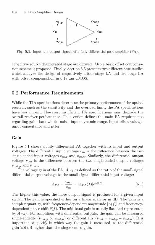
108 5 Post-Amplifier Design
vin,p
vin
vin,n vout,n
vout,p
vout
Fig. 5.1. Input and output signals of a fully differential post-amplifier (PA).
capacitive source degenerated stage are derived. Also a basic offset compensa-tion scheme is proposed. Finally, Section 5.5 presents two different case studieswhich analyze the design of respectively a four-stage LA and five-stage LAwith offset compensation in 0.18 µm CMOS.
5.2 Performance Requirements
While the TIA specifications determine the primary performance of the opticalreceiver, such as the sensitivity and the overload limit, the PA specificationshave less impact. However, insufficient PA specifications may degrade theoverall receiver performance. This section defines the main PA requirementsregarding gain, bandwidth, noise, input dynamic range, input offset voltage,input capacitance and jitter.
Gain
Figure 5.1 shows a fully differential PA together with its input and outputvoltages. The differential input voltage vin is the difference between the twosingle-ended input voltages vin,p and vin,n. Similarly, the differential outputvoltage vout is the difference between the two single-ended output voltagesvout,p and vout,n.
The voltage gain of the PA, APA, is defined as the ratio of the small-signaldifferential output voltage to the small-signal differential input voltage:
APA =vout
vin= |APA(f)|ejθ(f). (5.1)
The higher this value, the more output signal is produced for a given inputsignal. The gain is specified either on a linear scale or in dB. The gain is acomplex quantity, with frequency-dependent magnitude |A(f)| and frequency-dependent phase-shift θ(f). The mid-band gain is usually flat, and representedby APA,0. For amplifiers with differential outputs, the gain can be measuredsingle-endedly (vout,p or vout,n) or differentially (vout = vout,p − vout,n). It isimportant to specify in which way the gain is measured, as the differentialgain is 6 dB higher than the single-ended gain.

5.2 Performance Requirements 109
Bandwidth
The upper frequency at which the small-signal gain has dropped 3 dB belowits mid-band value, is defined as the PA bandwidth, BWPA.
The definition for bandwidth is based on the assumption that the amplifieroperates in its linear regime: when a sine wave is applied at the input, theamplifier produces a sine wave at the output. For a LA, this is not always thecase, certainly not in the last stages of the amplifying chain where clipping ofthe signal occurs. Then the concept of bandwidth no longer applies and mustbe replaced by a large-signal concept such as the switching speed. However,it is always possible to reduce the input signal amplitude to the point wherethe LA enter the linear regime. The small-signal bandwidth also tends to bea conservative estimate for the large-signal speed of the amplifier.
Remember from Section 4.2 that the bandwidth of a TIA is set to ap-proximately 0.7 times the bitrate Rb to limit the noise. Limiting amplifiers onthe other hand have a much larger bandwidth, usually equal to the bitrateRb [Raz03, Sac05].
Noise
The noise generated by the LA adds to the total optical receiver noise andthus degrades the receiver sensitivity. The overall integrated equivalent input-referred noise current of the optical receiver i2n,OR can be expressed as:
i2n,OR = i2n,TIA +v2
n,LA
Z2TIA,0
. (5.2)
i2n,TIA is the integrated input-referred noise current of the TIA (4.3). Thesame way, v2
n,LA is the integrated equivalent noise voltage at the input ofthe LA. Referred to the input of the optical receiver, it is divided by thetransimpedance gain. For a receiver sensitivity predominantly determined bythe noise of the TIA, the second term in (5.2) must be as small as possible.This becomes more critical for the following reasons:
• The large bandwidth required for the post-amplifier yields a greater totalintegrated noise.
• The design of TIAs with a high transimpedance gain becomes increasinglymore difficult at high speeds, making the noise of the post-amplifier moresignificant.
Input Dynamic Range
The input dynamic range of the LA describes the minimum and maximuminput signal for which the LA performs a useful function, in other words forwhich the BER is sufficiently low. The minimum input signal is determined

110 5 Post-Amplifier Design
by the sensitivity of the LA. Similar to the receiver sensitivity defined inSection 2.4.2, it is the minimum peak-to-peak signal voltage at the input ofthe LA necessary to achieve a specified BER. The maximum input signalswing is reached when the LA produces so much pulse-width distortion andjitter that the specified BER cannot be maintained.
Input Offset Voltage
The input offset voltage, Vos, is the differential input voltage for which thedifferential output voltage of the PA becomes zero. Even a small input offsetvoltage may drive the last stages of the LA in saturation. For this reason,limiting amplifier usually incorporate offset compensation.
Input Capacitance
The LA must exhibit a sufficiently low input capacitance so that it doesnot reduce the TIA bandwidth significantly. Therefore, the input transistorsshould be small, but this will lead to a smaller gain for the first stage.
Jitter
LAs may introduce jitter in the signal. It is desirable to maintain this jitterbelow a few percent of the bit period.
5.3 Literature Examples
A cascade of simple resistively-loaded differential pairs often proves inadequateas broadband amplifier, especially if the input amplitude is small and thefirst stages operate linearly. This is mainly due to the limited fT of today’smainstream CMOS technologies. Dedicated technologies such as GaAs or SiGehave a much higher fT , making it possible to design high-speed amplifiers withbasic differential amplifying stages [Max05]. This section gives a survey of thegain-bandwidth extension techniques used in the design of broadband LAs.Because interest in broadband amplifiers has always been high, some of thecircuits discussed already date from the 60’s.
A common way to increase bandwidth is to use inductive peaking. Anintegrated passive inductor is placed in series with the load resistor at thedominant node. The capacitance which limits the bandwidth at this node willresonate with the inductor. This results in a transfer function with a resonancepeak around the former 3-dB frequency and an extension of the bandwidth.The resonance must occur with minimal peaking and overshoot to provide awell-behaved response to random data with small BER. Major disadvantageof this approach is the large chip area required by the integrated inductors.

5.3 Literature Examples 111
Furthermore, accurate modeling of the electro-magnetic field is needed tocharacterize the inductors with their parasitics and to predict the overall cir-cuit performance. This approach has lead to a successful LA implementationin [Gal03]. The proposed LA consists of a broadband input-matching network,five identical gain stages comprising the LA core, an offset cancellation feed-back loop and an output buffer. Besides inductive peaking, other techniqueswhich are used to improve the gain-bandwidth of the gain stages are activefeedback and a negative Miller capacitance. This way, a 3-dB bandwidth of9.4 GHz has been realized with an overall differential gain of 50 dB. The sen-sitivity is 4.6 mVpp at 10 Gbit/s for a BER of 10−12. The power dissipation ofthe core amplifier is 100 mW, while the buffer consumes 30 mW. Total powerconsumption of the complete chip equals 150 mW from a 1.8 V power supply.One year later, the same authors propose a 40 Gbit/s LA [Gal04]. A triple-resonance structure is introduced which adds an extra inductor between twoinductively peaked gain stages. Five differential triple-resonance stages pro-vide an overall differential gain of 15 dB. Measurements of the single-endedoutput eyes are shown for input levels of 20 mVpp, 50 mVpp and 100 mVpp.Comparing these eyes with the simulations, results in an estimated small-signal bandwidth of 22 GHz. The circuit consumes 190 mW from a 2.2 Vpower supply.
To circumvent the area problem of passive integrated inductors, activeinductors can be used to create gain peaking, as in [Sac00]. The proposed LAconsists of four inversely scaled gain stages and an output buffer. The firststage is a common-gate differential pair, providing a low impedance input(50 Ω). The three following stages are common-source differential pairs, andthe last stage is implemented as a source follower. All gain stages have activeinductor loads consisting of an nMOS transistor operating in saturation anda gate resistor. The amplifier is implemented in a standard 2.5 V 0.25 µmCMOS technology and consumes 53 mW. The differential gain equals 32 dB.With a bandwidth of 3 GHz, eye diagrams at 2.5 Gbit/s showing little ISI aremeasured. One reason for not using active inductors is that they need a biasvoltage larger than Vdd to eliminate headroom difficulties. Furthermore, theyare unfavorable for noise performance.
The LAs presented in this work are based on the circuits first introducedby Cherry and Hooper in the early 60’s. In [Che63], they describe a designtechnique for the design of broadband transistor video amplifiers. As the am-plifiers in that era were realized with discrete components, emphasis lies onthe fact that gain and bandwidth should be insensitive to transistor parametervariations. The technique is based on the use of impedance mismatch whichoccurs between stages having alternate series and shunt feedback. The series-series feedback stage in Fig. 5.2(a) has a high input and output impedance,whereas the shunt-shunt feedback stage in Fig. 5.2(b) has a low input andoutput impedance. In order to stabilize the transconductance of the series-series feedback amplifier, RE should be large enough. The transconductanceis than approximated by 1/RE. In order to stabilize the transresistance of

112 5 Post-Amplifier Design
RE CE
Iout
RL
Vin
(a)
Iin
RF
CF
outV
RL
(b)
Fig. 5.2. Single-stage feedback amplifiers after Cherry and Hooper [Che63]: (a)series-series feedback stage, (b) shunt-shunt feedback stage.
a shunt-shunt feedback amplifier, it is necessary to make RF /RL sufficientlysmall, so that the transresistance is determined in first order by RF . Due tothe impedance mismatch between these stages, there is almost no interactionwhen they are cascaded. The overall gain may be calculated fairly accuratelyby simply multiplying the individual gain stages. When a series-series stage isfollowed by a shunt-shunt stage, the approximate voltage gain is thus RF /RE.By adding the high-frequency peaking components CE and CF , the authorsshow that the circuits are capable of reaching a gain-bandwidth product perstage equal to fT , which is the theoretical gain-bandwidth limit for an idealtransistor.
In the 80’s and early 90’s, the techniques introduced by Cherry andHooper have been adopted in the design of wideband amplifiers for opticalcommunication networks [Fau83, Rei87, Poh94]. The circuits are integratedin bipolar silicon technologies. The gain stage consists of a differential transad-mittance stage (TAS) with series-series feedback, followed by a differentialtransimpedance stage (TIS) with shunt-shunt feedback, and usually two emit-ter followers. Sometimes the series feedback resistance RS is omitted. This ispossible if the gain peaking introduced by RS and CS is not needed to achievethe required bandwidth. The major advantage is that the gain of the TAS-stage, which is determined by the gm of the input transistor, can be madelarger now. This results in less stages for the overall LA. The 3-stage LA pre-sented by [Fau83] is implemented in a 5 µm bipolar technology. The gain is60 dB while the bandwidth equals 470 MHz. Four years later [Rei87] presentsa 2 µm bipolar LA characterized by a gain of 54 dB and an operating speedof 4 Gbit/s. The LA consists of three equal gain stages, an output buffer, anemitter-follower input stage and offset control. Finally, the authors of [Poh94]use a 0.4 µm bipolar technology to implement a 10 Gbit/s LA with 45 dBgain. Also this amplifier consists of three gain stages, an output buffer, anemitter-follower input stage and offset control. The major high-level difference

5.4 Design of a Fully Differential Broadband LA 113
with [Rei87] is that the last gain stage is a distribution amplifier, where eachoutput of a series-series feedback stage drives two parallel feedback stages.This way, the signal is distributed to two differential outputs. However, theauthors also report that the higher loading of the stage cause an increase inthe jitter. To keep this jitter within acceptable limits, the gain of this lastgain stage is reduced. So a doubling of the output pads comes at the expenseof a lower gain, while no motivation is given in the paper for the need of twodifferential output signals.
Almost ten years after the > 10 Gbit/s bipolar PAs [Poh94, Mol94], thefirst Cherry-Hooper amplifier implemented in a CMOS technology is presentedby [Hol03]. A test circuit, implemented in a 0.35 µm CMOS technology has9.4 dB gain and 880 MHz bandwidth. In addition, a six-stage 0.18 µm CMOSpost-amplifier using modified Cherry-Hooper stages is presented. It has 43 dBdifferential gain and 2.1 GHz bandwidth. Whereas the authors of [Hol03] havedemonstrated the usefulness of Cherry-Hooper stages in CMOS, the goal ofthis work is to extend the achievable bitrates further in the Gbit/s range.Furthermore will the described LA be integrated with TIA and PD to presenta single-chip solution for optical front-end receivers.
5.4 Design of a Fully Differential Broadband LA
Most of today’s high-performance post-amplifiers employ a differential topol-ogy. The main advantage of differential operation over single-ended signalingis a higher immunity to environmental noise. Ground and power supply dis-turbances, originating for instance from the clock and data recovery circuit,will corrupt the signal lines, but the differential (output) signal will remainintact. So differential circuits are characterized by a high common-mode re-jection ratio (the differential gain divided by the common-mode rejection,where common-mode rejection is defined as the differential output voltage fora common-mode input voltage, when the differential input voltage is zero) anda high power supply rejection ratio (the gain from the input to the outputdivided by the gain from the power supply to the output). Differential linesare not only beneficial for sensitive signals, but also for noisy signals. Theseare for instance present in the last stages of the LA, where the signals havean amplitude of a few 100 mV and change rapidly. Due to the differentialnature of the amplifier, the total current drawn from the power supply re-mains more or less constant, and alternates between the two branches of thedifferential stage. This way, the stage presents a constant load to the powersupply, resulting in less noise generated in the power supply. On the otherhand, due to a doubling of the devices in a differential circuit, the input noisevoltage is always
√2 larger than in a single-ended amplifier. However, for the
post-amplifier, this drawback does not counterweigh the many advantages ofa differential topology.

114 5 Post-Amplifier Design
This section discusses the main topics related to the design of broadbandlimiting amplifiers. First, the effect of cascading several amplifying stages isexamined. Next, some broadband amplifying stages are studied, where thefocus lies on combining both high bandwidth and high gain using analogcircuit design techniques. Finally, a basic technique for offset compensation ispresented.
5.4.1 Cascaded Gain Stages
As the broadband LA requires both high gain and high bandwidth, cascadingseveral amplifying stages is required to achieve a high gain-bandwidth prod-uct. Assume N second-order stages are cascaded, the overall transfer functionis given by:
APA =
(A1st,0
( sωn
)2 + 2ζ( sωn
) + 1
)N
, (5.3)
where A1st,0 is the DC voltage gain for one single stage. So the more stagesare cascaded, the higher the overall small-signal DC gain APA,0, as it equals:
APA,0 = AN1st,0. (5.4)
As already mentioned in Section 4.3.1, a second-order system with ζ =√
2/2has a maximally flat response and corresponds to a second-order Butterworthfilter. Also, it can be proven that for this type of filter ωn = ω3dB. Underthese conditions, the overall bandwidth of a PA consisting of N cascadedsecond-order Butterworth stages is given by:
f3dB,PA = f3dB,1st4√
N√
2 − 1. (5.5)
So the higher N, the smaller the overall bandwidth f3dB,PA, or the higherthe required bandwidth per stage f3dB,1st to attain a predetermined overallbandwidth.
The gain-bandwidth extension of N cascaded stages compared to a singlestage is:
GBWPA
GBW1st= A
1−1/NPA,0
4√
N√
2 − 1. (5.6)
This function increases for increasing N due to the rising gain when stages areadded. However, owing to the smaller bandwidth with increase of N , the func-tion saturates and reaches a maximum. The number of stages correspondingto this maximal GBWPA can be found using following approximation:
f3dB,PA ≈ f3dB,1st0.94√
N, (5.7)
which is valid for large enough values of N . Using this approximation, (5.6)reduces to:

5.4 Design of a Fully Differential Broadband LA 115
0 5 10 15 200
5
10
15
20
25
30
Number of stages N
GB
WP
A/GB
W1s
t
APA,0
=20
APA,0
=40
APA,0
=60
Fig. 5.3. Gain-bandwidth extension as a function of the number of stages N in apost-amplifier.
GBWPA
GBW1st≈ APA,0
N√
APA,0
0.94√
N. (5.8)
To minimize the denominator D = 4√
N N√
APA,0, the natural logarithm istaken and differentiated with respect to N :
1D
dD
dN=
14N
− 1N2
ln APA,0. (5.9)
This equation becomes zero for N = 4 lnAPA,0.The gain-bandwidth extension given by (5.6) is plotted versus the number
of stages N for three different values of the overall gain APA,0 in Fig. 5.3. Theoptimal N corresponding to a maximal GBW is quite high: for APA,0 = 20,N = 12; for APA,0 = 40, N = 14; for APA,0 = 60, N = 16. However, the plotalso reveals only an incremental change in GBWPA/GBW1st for values aroundthe optimal N . For instance, when APA,0 = 20 and as N goes from 5 to 12,the ratio GBWPA/GBW1st only increases by 11 %. Furthermore, when N ishigh, the gain per stage is small, making the noise contributed by all of thestages significant. Finally, a lot of stages also corresponds to a high powerdissipation and a large chip area. For these reasons, typical high-gain LAsemploy no more than five stages.
For example, assume a 3 GHz 30 dB PA has to be designed. Usingsecond-order Butterworth stages, the optimal N is 14 and the correspondinggain-bandwidth extension GBWPA/GBW1st is 11.7. However, for the reasonsmentioned above, some stages may be left out. For N = 4, the gain-bandwidthextension is still 8.8. Each stage needs a GBW1st of 11 GHz, which is realizedwith a gain of 7.5 dB and a bandwidth of 4.6 GHz.

116 5 Post-Amplifier Design
5.4.2 Broadband Cherry-Hooper Stage
Classical Cherry-Hooper Amplifier
As discussed in Section 5.3, a technique used for many years to enhance thebandwidth of a differential amplifier is the Cherry-Hooper topology. A CMOSimplementation is depicted in Fig. 5.4(a). Transistors M1 and M2 form theinput pair, and resistor Rf provides feedback between the drain and gateof transistor M3 respectively M4. Rd is the load resistor. Using the originalterminology of Cherry, Hooper [Che63] and their followers, transistors M1
and M2 form a differential TAS-stage with transadmittance gain gm,M1. M3,M4 and Rf constitute a differential TIS-stage with shunt feedback and withtransimpedance gain Rf .
The small-signal half circuit is shown in Fig. 5.4(b). The output resistancesof the transistors are usually larger than Rf and Rd, so they are omitted. Thedifferential small-signal gain ACH of this stage is given by:
ACH = ACH,0
1 − sCgd,M3gm,M3
s2 Rf
gm,M3C2 + s(RC)CH + 1
, (5.10)
with:
ACH,0 = gm,M1Rf , (5.11)C2 = C1Cgd,M3 + C1CL + Cgd,M3CL, (5.12)
(RC)CH = RfCgd,M3 +Rf + Rd
Rdgm,M3C1 +
CL
gm,M3. (5.13)
C1 is the total parasitic capacitance at node n1, Cgd,M3 is the gate-drain ca-pacitance of transistor M3 and CL is the total capacitance at the output noden3. These equations are valid as long as gm,M3Rf >> 1 and gm,M3Rd >> 1.
As expected, the small-signal gain of the Cherry-Hooper amplifier at lowfrequencies (5.11) is given by the product of its transadmittance gain and itstransimpedance gain. This product is comparable to the gain of a differentialpair because the load resistor of a differential stage is of the same order ofmagnitude as the feedback resistor Rf . However, the bandwidth of this stagecan be seriously extended. Assuming that the denominator of (5.10) showstwo separated poles, the dominant pole is in first order given by 1/(RC)CH .Mostly, Cgd,M3 is much smaller than C1 and CL, so the first term in (5.13)can be neglected. If it further can be assumed that Rd >> Rf , the pole atnode n1 equals gm3/C1, and the pole at node n3 is given by gm3/CL. Whichof these nodes determines the dominant pole depends on the relative valuesof C1 and CL. In any case, the resistance seen by the dominant pole is only1/gm,M3. In a simple differential stage, the dominant pole is determined bythe load capacitance CL and the output resistance. The latter one is usuallymuch larger than 1/gm3, resulting in a smaller bandwidth.

5.4 Design of a Fully Differential Broadband LA 117
M1Vin1 M2
Vin2
Mc4
Mc2
Mc3
Vdd
RdRd
Rf
M3 M4
Rf
I2
I1n2n1
n3 n4Vout2Vout1
Mc1
(a)
C1
Rf
Cgd,M3
gm,M3 gs,M3vgm,M1inv
2
outv
CLRd
2n3n1
(b)
Fig. 5.4. CMOS Cherry-Hooper amplifier stage: (a) schematic, (b) small-signal halfcircuit.
If the design goal of this stage is to optimize bandwidth, the poles willnot be separated, but complex conjugated. However, the above reasoning isvery valuable for gaining insight in the major advantages of the Cherry-Hoopertopology. Gain-bandwidth of the stage is enlarged by moving the poles towardshigher frequencies, without the penalty of loosing significant gain.
Modified Cherry-Hooper Amplifier
One can even go a step further in improving the performance by raising thegain, without a corresponding decrease in bandwidth. This is realized by the

118 5 Post-Amplifier Design
M1Vin1 M2
Vin2
Mc4
Mc2
RfRf
M5 M6
Mc3
Mc1
Vdd
M4
Vout2
M3
R2 R2
Vout1
R1 R1
I2
I1n2
n6
n3b n4b
n1
n5n3 n4
(a)
Cgd,M3
C1
Rfgm,M1inv
2gm,M5 gs,M5v gm,M3 gs,M3v
outv
2
CL
R2
R1
n3b
n3n5n1
(b)
Fig. 5.5. Modified CMOS Cherry-Hooper amplifier stage: (a) schematic, (b) small-signal half circuit.
modified Cherry-Hooper amplifier, depicted in Fig. 5.5(a). This stage was firstintroduced in CMOS by [Hol03]. Compared to a traditional Cherry-Hooperstage, resistor Rd is split up in two resistors R1 and R2, and transistorsM5-M6 provide source follower feedback. The small-signal half circuit is shownin Fig. 5.5(b), where again the output resistances of the transistors are leftout. The differential small-signal gain AMCH is now given by:
AMCH = AMCH,0
1 − sCgd,M3gm,M3
s2(RC)2MCH + s(RC)MCH + 1, (5.14)

5.4 Design of a Fully Differential Broadband LA 119
with:
AMCH,0 = gm,M1RffMCH , (5.15)
fMCH = 1 +R2
R1, (5.16)
(RC)2MCH =AMCH,0
gm,M1gm,M3C2, (5.17)
C2 = C1Cgd,M3 + C1CL + Cgd,M3CL, (5.18)
(RC)MCH = RfCgd,M3fMCH +Rf
R1gm,M3C1 +
fMCH
gm,M3CL. (5.19)
Again, C1 is the total parasitic capacitance at node n1, Cgd,M3 is the gate-drain capacitance of transistor M3 and CL is the total capacitance at theoutput node n3. This time, the equations are valid as long as gm,M5Rf >> 1and gm,M3R1 >> 1.
By comparing (5.11) and (5.15), one can see that the gain at low frequen-cies is raised in the modified topology with the factor fMCH . This factor ismainly determined by the ratio of R2 and R1. To increase gain, this ratiomust be large. Because this factor is determined by a ratio of resistors, it isless sensitive to process modifications.
The topology of Fig. 5.5 has some limitations. The major one is the smallvoltage headroom available in recent CMOS technologies. This problem willonly get worse as linewidth scales down and consequently the available powersupply drops. First, when cascading several stages, the ratio R2/R1 can notbe made extremely large, as the DC voltage at nodes n3 and n4 must besufficiently high to drive the next stage. Second, a critical path exists betweenpower supply and ground, where attention must be paid to keep all transistorsin saturation. The path is formed by the voltage drop over R1, the gate-source voltage of transistor M5 (Vgs,M5), the voltage drop over Rf , the gate-source voltage of transistor M3 (Vgs,M3) and finally the drain-source voltage ofbiasing transistor Mc3 (Vds,Mc3). In a 0.18 µm CMOS technology, the VT of annMOS transistor is typically 0.5 V. For a traditional overdrive voltage Vgs−VT
of 0.2 V, Vgs,M3 and Vgs,M5 must be equal to 0.7 V. Vds,Mc3 should be largerthan the saturation voltage, which approximately equals the overdrive voltageVgs − VT of 0.2 V. As a result, the voltage drop consumed by the transistorsis as large as 1.6 V. With a power supply of 1.8 V, only 0.2 V is left for theresistors. Therefore, the current through these resistors is usually low and theresistance values are designed as small as possible within the constraint ofhigh gain. Design values will be given in Section 5.5. The result is that theapproximation gm,M5Rf >> 1 is not longer valid, and the small-signal DCgain is more accurately modeled by:
AMCH,0 =gm,M1(R1 + R2)(1/gm,M5 + Rf )
R1 + 1/gm,M3. (5.20)

120 5 Post-Amplifier Design
Another important issue is the influence of the ratio R2/R1 on the band-width, as fMCH also appears in (RC)2MCH and (RC)MCH . Simulationsof (5.14) show that a large ratio, which is needed for large gain, also re-sults in two real separated poles, which is less beneficial for bandwidth. Thisshould be avoided, and the design must focus on optimizing both gain andbandwidth by introducing complex conjugated poles.
Finally, as the circuit of Fig. 5.5(a) has a feedback loop consisting of M5,Rf , M3, R1 and R2, care should be taken to ensure stability. By cutting theloop for example at node n3b, following loop gain LMCH can be found:
LMCH = −LMCH,0
1 − sCgd,M3gm,M3
s2(RC)2LCH + s(RC)LCH + 1, (5.21)
with:
LMCH,0 = gm,M3R1, (5.22)(RC)2LCH = Rf (R1 + R2)C2, (5.23)(RC)LCH = Rfgm,M3(R1 + R2)Cgd,M3 + RfC1 + (R1 + R2)CL. (5.24)
C2 is given by (5.18), and it is supposed that gm,M5Rf >> 1 andgm,M3R1 >> 1. Just like the small signal gain (5.14), the loop gain has apositive zero. This is dangerous for the phase margin, as it introduces a phaserotation of −90◦. So the stability of this loop has to be monitored very closelyduring the optimization of the gain-bandwidth.
5.4.3 Broadband Stage with Capacitive Source Degeneration
When the disadvantages of the Cherry-Hooper stage cannot be tolerated, abroadband stage must be realized in a different way. Fig. 5.6 shows the circuitdiagram of a differential voltage amplifier stage with capacitive and resis-tive source degeneration. In order to create a broadband response, the inputtransistors M1a and M1b are degenerated such that their effective transcon-ductance increases at high frequencies. This requires that resistor Rs andcapacitance Cs are placed between the sources of the transistors.
The effective transconductance Gm,CSD of the half-circuit equivalent isgiven by:
Gm,CSD =gm,M1
1 + gm,M1
(Rs
2 // 12sCc
) ,
=gm,M1(sRsCs + 1)
sRsCs + 1 + gm,M1Rs
2
. (5.25)
The zero introduced by Rs and Cs causes the effective transconductance toincrease at higher frequencies. The same zero appears in the transfer functionACSD of the simplified small-signal half circuit depicted in Fig. 5.6(b):

5.4 Design of a Fully Differential Broadband LA 121
Vin1 Vin2
Vout1 Vout2
Ms1
Vdd
Ms2
M1a
Cs
I1
Ms3
R1a R1b
Rs
M1b
n1a n1b
n2a n2b
(a)
Rs Cs
svR1
outv
2
gm,M1 svinv
2( )
2
2
LCn2
n1
(b)
Fig. 5.6. Voltage amplifier with source degeneration: (a) schematic, (b) small-signalhalf circuit.
ACSD = −ACSD,01 + sRsCs(
1 + sCLR1
)(1 + s RsCs
1+gm,M1Rs2
) , (5.26)
with:ACSD,0 =
gm,M1R1
1 + gm,M1Rs
2
≈ 2R1
Rs. (5.27)
The approximation in (5.27) holds for gm,M1Rs � 1. The voltage gain of thesource degenerated amplifier features two poles. The first one is determinedby the load at the output node n1, formed by CL and R1. The other pole is aresult of the source degeneration, and a factor (1 + gm,M1Rs/2) higher thanthe corresponding zero. Bandwidth extension is obtained if the zero cancelsthe pole at node n1, so if:

122 5 Post-Amplifier Design
RsCs = R1CL. (5.28)
The 3dB-bandwidth of this stage is than given by:
BWCSD =1 + gm,M1
Rs
2
2πR1CL, (5.29)
which is a factor (1 + gm,M1Rs/2) higher than the bandwidth of a traditionaldifferential stage with input transistor M1 and load R1. However, this band-width extension comes at the price of a lower gain, which is reduced by thesame factor (5.27). Compared to a Cherry-Hooper stage where both gain andbandwidth are extended, the voltage amplifier with source degeneration hasa lower gain-bandwidth product, but is less complex to design, has a lowerpower consumption, shows less problems with a low voltage headroom and iscapable of a high output swing.
5.4.4 Offset Compensation
According to [Sac05], the input offset voltage of an LA should be limited toabout 0.1 mV, while a high-speed MOSFET amplifier has a 3σ random offsetvoltage of around 10 mV. An offset compensation circuit is needed to reducethe offset voltage to the required value. Fig. 5.7 shows a classical implemen-tation of an offset feedback compensation scheme, which will also be used inthe LA studied in Section 5.5.2. The DC value at the output of the two sig-nal paths is measured through the low-pass filter Ros-Cos. The output offsetvalue (the DC component of the differential output signal) is measured andamplified with a simple resistively loaded stage with voltage gain Aos. Theresulting signal is fed back to the input to take corrective actions until theoutput offset voltage becomes zero.
The offset compensation circuit not only suppresses the unwanted offsetvoltage, but also some important low-frequency components of the input sig-nal. In other words, the offset compensation introduces a low-frequency cut-offin the overall LA frequency response. As discussed in Section 2.5.2 and Sec-tion 2.6, a low-frequency cut-off causes baseline wander and data-dependentjitter if the cut-off frequency is too high. For the configuration of Fig. 5.7, thecut-off frequency is given by:
fLF =APAAos + 12πRosCos
. (5.30)
Note that APAAos is the loop gain of the offset compensation loop. As ahigh gain APA is one of the primary specifications of the PA, the values ofRos and Cos must be quite large to obtain a small cut-off frequency. In CMOStechnologies, these high values can be realized by using some analog extensionswhich have become widespread: MiM-capacitors with a high capacitance perunit square and high-ohmic poly-resistors.

5.4 Design of a Fully Differential Broadband LA 123
A1st A1st A1st
Aos
Vin Vout
Ros
RosCos
Cos
APA
Fig. 5.7. Block diagram of an LA with offset compensation.
While a low cut-off frequency is needed to minimize ISI and jitter, themain disadvantage is the long compensation settling time. For most point-to-point communication links, long compensation times are acceptable, but theypose a severe obstacle for upcoming many-to-one links like passive opticalnetworks. Each input channel may have different power levels and thereforedemand different offset settings of the amplifier. The speed of the offset com-pensation loop will therefore determine how quickly one can change betweenchannels. Therefore [Cra05] proposes a peak detector structure and a variable-tap feedback system to improve the trade-off between settling time and data-dependent jitter. The offset of the differential amplifier is not estimated fromthe difference in DC values of its two outputs, but from the difference in peakvalues of its outputs. So a peak detector measures the output offset voltage ofthe LA, and an integrator filters the instantaneous peak detector output andforces the steady-state output offset voltage to be zero. Since peak informationis lost when the gain stages of the LA become saturated, peak detectors areplaced at the output of each LA stage and the last unsaturated output is usedto sense the offset. To demonstrate the technique, a 7-stage LA is fabricatedin a 0.18 µm CMOS process. The prototype is tested up to 3.125 Gbit/s withinput amplitudes ranging from 2.5 mVpp to 50 mVpp. The total differentialgain is 42 dB. Offset settling times less than 1 µs are measured while stillmaintaining SONET OC48 jitter levels.
Finally note that often a 50 Ω matching network at the input of the LAis included with the offset compensation circuit, as for example in [Poh94,Gal03, Sac05]. This is especially necessary for stand-alone amplifiers which areexpected by the (measurement) equipment to have a 50 Ω input impedanceand to drive a 50 Ω load. As the ultimate goal of this work is to integrate acomplete opto-electrical analog front-end with PD, TIA and LA, the issue ofinput matching is not addressed.

124 5 Post-Amplifier Design
5.5 Case Studies
The design simulations of two LAs are considered in this section. The focuslies on the primary specifications of the PA, namely gain and bandwidth.First a LA with four cascaded Cherry-Hooper stages is discussed, second afive-stage LA with offset compensation is described. The measurement resultsof these LAs, realized together with high-speed output buffers in a 0.18 µmCMOS technology, will be treated in Section 6.4 and in Section 6.5.
5.5.1 A Four-Stage LA in 0.18 µm CMOS
This LA consists of a plain cascade of the modified Cherry-Hooper stagesdepicted in Fig. 5.5. Whereas in [Fau83, Rei87, Poh94, Hol03] emitter or sourcefollowers are placed between the cascaded stages, they are omitted in thedescribed implementation, as they only degrade the gain performance. Currentbranches I1 with diode-connected transistor Mc2 and I2 with diode-connectedtransistor Mc4 are common to all stages. As derived in Section 5.4.2, the majoradvantage of the modified Cherry Hooper stage over a simple resistively-loadeddifferential stage, is an increase in both gain and bandwidth.
The most important design parameters are summarized in Table 5.1. Alltransistors, except for the common-mode current source transistors, have min-imal gate length. Due to the limited voltage headroom of 1.8 V, the saturationvoltage VDSAT (≈ VGS − VT ) of the high-frequency transistors is slightly be-low 0.2 V. The gate length L of the current mirror transistors is not chosenminimal, but equals 0.8 µm, for the following reasons:
• In [San06] it is shown that the current difference in the mirror is propor-tional to the difference in drain-source voltage, and inversely proportionalto the product of Early voltage and channel length L. The larger L, theflatter the Ids-Vds curve and the smaller the current difference betweentwo transistors with unequal drain-source voltages.
• The CMOS current and VT mismatch parameters are inversely propor-tional to the square root of the area WL of the transistor.
Note also that Rf is as small as 40 Ω to limit the voltage drop over thisresistor. Drawback is a smaller DC gain (5.15).
In Fig. 5.8 the simulated frequency response for one stage and for the com-plete LA is depicted. The gain per stage equals 6.8 dB, which results in anoverall gain of 27.4 dB. The first stage is slightly different from the followingstages, as an LC input network is included in the simulations to take bond-wires, bond pads and ESD-protection into account. This stage is of third orderand has a bandwidth of 5.2 GHz. The next stages are all second order stagesand have a 3-dB frequency equal to 6.7 GHz. Their gain-bandwidth prod-uct equals 14.6 GHz. The LA has an overall simulated bandwidth of 4 GHz,which corresponds quite well with the bandwidth predicted by (5.5). The gain-bandwidth of the complete LA is 94 GHz, so the gain-bandwidth extension as

5.5 Case Studies 125
106
107
108
109
1010
−20
−10
0
10
20
30
frequency [Hz]
gain
[dB
]
1st stage2nd stage3th stageoutput
(a)
106
107
108
109
1010
−5
0
5
10
frequency [Hz]
gain
[dB
]
first CH stageother CH stages
(b)
Fig. 5.8. Simulated gain of the four-stage LA: (a) gain after each stage and at theoutput, (b) gain of the individual building blocks.
Table 5.1. Design parameters of the Cherry-Hooper stage in the four-stage LA.
M1/M2 M3/M4 M5/M6
type nMOS nMOS nMOS
L 0.18 µm 0.18 µm 0.18 µm
W 34 µm 44 µm 36 µm
VDSAT 0.17 V 0.17 V 0.16 V
IDS 0.78 mA 1.1 mA 0.78 mA
gm 7.5 mS 11 mS 8.1 mS
gds 0.46 mS 0.39 mS 0.32 mS
Cgs 44 fF 56 fF 47 fF
Cgd 12 fF 16 fF 13 fF
I1 1.6 mA
I2 2.5 mA
R1 200 Ω
R2 400 Ω
Rf 40 Ω
defined in (5.6) equals 6.4. The circuit with biasing consumes 19 mA from a1.8 V power supply. Compared to recently published papers in 0.18 µm CMOS([Hol03, Gal03, Gal04, Cra05], see Table 6.8), the gain-bandwidth product ofthis circuit is not that high, but the power dissipation is very low: comparedto [Gal04], the power dissipation is almost six time smaller.

126 5 Post-Amplifier Design
5.5.2 A Five-Stage LA with Offset Compensationin 0.18 µm CMOS
The block diagram of the second LA is depicted in Fig. 5.9. It consists of aninput buffer, five fully differential amplifying stages and offset compensationfeedback. The first two stages are non-inverting Cherry-Hooper stages withnegative impedance converters (CH with NIC), the last three stages are in-verting voltage amplifiers with capacitive source degeneration (VA with CSD).The circuit schematic of the input buffer and the offset compensation circuitare shown in more detail. A positive offset voltage at the output of the LA willlead to nosp > nosn at the input of the offset compensation feedback ampli-fier. As a result, the current through Mos1a and consequently also through R1a
will increase. Analogously, the current through Mos1b and R1b will decrease.Therefore, the DC input voltage of ninp decreases while the DC input voltageof ninn increases, both compensating for the positive output offset voltage.The values of Ros and Cos, which make up the low-pass filter, must be chosencarefully. Too small values create a relatively high low-frequency cut-off. Asa result, lower frequency components in the prbs data are considered as DCvoltage variations and compensated for. On the other hand, large values of Ros
and Cos generate longer settling times. In the described design, the simulatedlow-frequency cut-off (5.30) is 700 kHz. The input stage acts as a buffer be-tween the previous building block (which is an analog equalizer as discussed inSection 6.5) on one hand and the first amplifying stage and the offset compen-sation amplifier on the other hand. To minimize the load on the equalizer, theinput transistors are very small (WM1 = 6 µm, LM1 = 0.18 µm). Capacitivesource degeneration is added to increase bandwidth.
A detailed circuit schematic of the modified Cherry-Hooper stage is de-picted in Fig. 5.10. To increase the bandwidth of this broadband stage evenfurther, a negative impedance converter (NIC) [Gal03] is added between out-put nodes n3 and n4. If the gate-drain capacitance of M7 and M8 is neglected,the impedance ZNIC between the drains is expressed by:
ZNIC = −gm,M7
sCc+ Cgs,M7
Cc+ 2
gm,M7 − sCgs,M7, (5.31)
where Cc is the compensation capacitance and Cgs,M7 is the gate-source ca-pacitance of transistors M7 and M8. Or, for frequencies well below the fT ofthe transistors:
ZNIC ≈ −( 1
sCc+
1gm,M7
(Cgs,M7
Cc+ 2
)). (5.32)
The impedance ZNIC consists of a capacitive part (−Cc) in series with a re-sistive part. This negative capacitance partly compensates for the capacitanceat nodes n3 and n4. However, a good design choice has to be made, as a toolarge value of Cc can cause gain peaking and ringing.

5.5 Case Studies 127
R1a R1b
n
Vdd
Cs
LA core
Vout
nosnospMos1a Mos1b
CosCos
Vin1 Vin2M1a
Rs
M1b
I1 I1
Ios
Ros
Ros
Vin
ninn
ninp
withNIC
CH CHwithNIC
VAwithCSD
VAwithCSD
VAwithCSD
noutp
noutn
Fig. 5.9. Block diagram of the five-stage LA with detail of the input buffer andoffset compensation circuit.
The design parameters of the CH stage with NIC are summarized in Ta-ble 5.2. To relax the biasing of the transistors in the critical pathR1-M5-Rf -M3-Mc3, and optimizing gain-bandwidth, zero-VT transistors areused for the source follower feedback transistors M5-M6. These transistors arestandard available in the 0.18 µm CMOS technology used, but have a min-imal gate length of 0.3 µm. Comparing the saturation voltages VDSAT withthe ones from the design discussed in Section 5.5.1, reveals that the saturationvoltages are higher and come closer to the traditional value of 0.2 V. The cur-rent mirror transistors have even higher values in order to generate a betterdefined current. Furthermore, the ratio R2/R1 and the feedback resistor Rf
have larger values in this design. Both measures result in a higher gain (5.15).Finally, note that the compensation capacitor Cc is realized as a series con-nection of two MiM-capacitors, with the common node connected to ground.This way, the parasitic capacitance to ground is effectively taken into accountduring simulations.
Since a large output swing is not possible with this bandwidth optimizedCherry-Hooper stage, a voltage amplifier with capacitive source degeneration(VA with CSD) is used in the last stages of the amplifying chain. The designequations of this stage have been discussed in Section 5.4.3 and the circuitschematic is shown in Fig. 5.6. The design parameters are given in Table 5.2.

128 5 Post-Amplifier Design
Rf
M5
Vdd
R1 R1
M4M8
C c
M7
Rf
M6
M1Vin1 M2
Vin2
M3
I3
I1I2
I3
R2
Vout1 Vout2
n3b
n5
n4b
n1
n6
n2
n3 n4
2R
NIC
Fig. 5.10. Modified CMOS Cherry-Hooper with negative impedance converter(NIC).
The source degeneration capacitor Cs is also realized as a series connection oftwo MiM-capacitors.
Finally, the simulated gain of the LA is depicted in Fig. 5.11(a) togetherwith the gain after each stage. The transfer function of the separate gain stagesis shown in Fig. 5.11(b). The CH stage with NIC has a simulated bandwidthof 7.6 GHz and a gain of 10 dB. The gain-bandwidth of this stage is 24 GHz,which is a gain-bandwidth improvement of almost 10 GHz compared to theCH stage discussed in Section 5.5.1. The source-degenerated amplifier has asimulated bandwidth of 9 GHz, which results with a gain of 6 dB in a gain-bandwidth of 18 GHz. The complete LA has a simulated small-signal gain of38 dB, an overall 3-dB bandwidth of 5 GHz and a gain-bandwidth as highas 397 GHz. This should be sufficient to amplify 5 Gbit/s data with a lowBER. The gain-bandwidth extension (5.6) over the Cherry-Hooper stage is16.5 while the gain-bandwidth extension over the source-degenerated ampli-fier is 22. Due to the offset compensation circuit, the transfer function hasa low-frequency cut-off of 700 kHz. This is still more than ten times smallerthan the smallest frequency component in 231-1 500 Mbit/s prbs data. Am-plifying data with a smaller bitrate or more consecutive ones and zeros mightresult in baseline wander. The on-chip simulated output swing is 1.2 Vpp.The LA consumes 40 mA from a 1.8 V power supply. Comparing these valueswith present state-of-the-art (Table 6.8), this amplifier competes with other
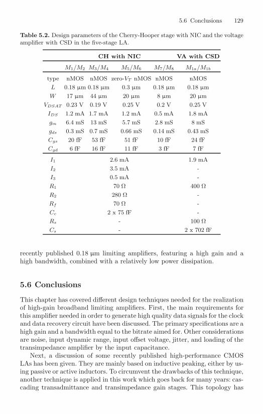
5.6 Conclusions 129
Table 5.2. Design parameters of the Cherry-Hooper stage with NIC and the voltageamplifier with CSD in the five-stage LA.
CH with NIC VA with CSD
M1/M2 M3/M4 M5/M6 M7/M8 M1a/M1b
type nMOS nMOS zero-VT nMOS nMOS nMOS
L 0.18 µm 0.18 µm 0.3 µm 0.18 µm 0.18 µm
W 17 µm 44 µm 20 µm 8 µm 20 µm
VDSAT 0.23 V 0.19 V 0.25 V 0.2 V 0.25 V
IDS 1.2 mA 1.7 mA 1.2 mA 0.5 mA 1.8 mA
gm 6.4 mS 13 mS 5.7 mS 2.8 mS 8 mS
gds 0.3 mS 0.7 mS 0.66 mS 0.14 mS 0.43 mS
Cgs 20 fF 53 fF 51 fF 10 fF 24 fF
Cgd 6 fF 16 fF 11 fF 3 fF 7 fF
I1 2.6 mA 1.9 mA
I2 3.5 mA -
I3 0.5 mA -
R1 70 Ω 400 Ω
R2 280 Ω -
Rf 70 Ω -
Cc 2 x 75 fF -
Rs - 100 Ω
Cs - 2 x 702 fF
recently published 0.18 µm limiting amplifiers, featuring a high gain and ahigh bandwidth, combined with a relatively low power dissipation.
5.6 Conclusions
This chapter has covered different design techniques needed for the realizationof high-gain broadband limiting amplifiers. First, the main requirements forthis amplifier needed in order to generate high quality data signals for the clockand data recovery circuit have been discussed. The primary specifications are ahigh gain and a bandwidth equal to the bitrate aimed for. Other considerationsare noise, input dynamic range, input offset voltage, jitter, and loading of thetransimpedance amplifier by the input capacitance.
Next, a discussion of some recently published high-performance CMOSLAs has been given. They are mainly based on inductive peaking, either by us-ing passive or active inductors. To circumvent the drawbacks of this technique,another technique is applied in this work which goes back for many years: cas-cading transadmittance and transimpedance gain stages. This topology has

130 5 Post-Amplifier Design
104
106
108
1010
−30
−20
−10
0
10
20
30
40
frequency [Hz]
gain
[dB
]
1st stage2nd stage3th stage4th stageoutput
(a)
106
107
108
109
1010
−5
0
5
10
frequency [Hz]
gain
[dB
]
CH with NICVA with CSD
(b)
Fig. 5.11. Simulated gain of the five-stage LA with offset-compensation: (a) gainafter each stage and at the output, (b) gain of the individual building blocks.
first been proposed by Cherry and Hooper in the early 60’s by using a cas-cade of series-series feedback and shunt-shunt feedback amplifiers. Later, thetechnique is taken over by BiCMOS and CMOS designers for the realizationof broadband amplifiers for optical communication networks.
The most important issues concerning the design of a broadband differ-ential LA have been treated in the following section. The optimal number ofstages as a compromise between gain-bandwidth, area, power dissipation andnoise has been found to be equal to five. An in-depth small-signal analysisof a Cherry-Hooper stage and a slightly modified Cherry-Hooper stage hasbeen given. The main improvement of this stage compared to a differentialstage with resistive loads, is an increase in both gain and bandwidth. Themain limitations are that a sufficiently high power supply is needed for DCbiasing and that the design complexity is rather high. As an alternative, abroadband voltage amplifier with capacitive and resistive source degenerationhas been implemented. This stage increases the bandwidth, but at the costof a corresponding decrease in gain. The implications of the traditional offsetcompensation feedback loop have been studied and an alternative solutionfrom literature based on peak detection and lower settling times has beendiscussed.
Finally, two different case studies have been presented to illustrate thetrade-offs encountered during the design of a LA. The first LA consists ofa simple cascade of four modified CMOS Cherry-Hooper stages. Each stagehas a bandwidth of 6.7 GHz and a gain of 6.8 dB. The total gain of the fourcascaded stages equals 27.4 dB, which results with an overall 4 GHz band-width in a gain-bandwidth product of 94 GHz. In the second LA design, thisgain-bandwidth factor is more than four times improved and equals 397 GHz.This is achieved by using two Cherry-Hooper stages with negative impedanceconverters and three source-degenerated voltage amplifiers. Moreover, this LA
5.6 Conclusions 131
features offset cancellation. The gain equals 38 dB and with a bandwidth of5 GHz a bitrate of 5 Gbit/s should be feasible with low BER. This circuit,characterized by a high gain-bandwidth product combined with a relativelylow power dissipation of 72 mW, outperforms most of the recently published0.18 µm CMOS limiting amplifiers. The measurement results of these twoLAs, including high-speed eye diagrams, will be shown in Chapter 6.

6
CMOS Realizations
6.1 Introduction
After the theoretical design of the CMOS PD, the TIA and the LA, thischapter deals with four practical CMOS realizations. The TIAs and LAs havebeen analyzed in previous chapters, only some additional building blocks likethe output buffers need to be covered here. The main focus lies on the mea-surements and the interpretation of the results. Each section is dedicated toa different implementation. In Section 6.2, test photodiodes with a TIA ina 0.18 µm CMOS technology are discussed, followed in Section 6.3 by testphotodiodes with a TIA in a 90 nm CMOS technology. The chip presentedin Section 6.4 contains a 0.18 µm LA and high-speed output buffer. Finally,the different building blocks are brought together in Section 6.5, where a com-pletely integrated 0.18 µm CMOS optical receiver, working at Gbit/s bitrates,is described.
One important challenge in opto-electronics is to focus the light from thetransmitter on the photodiode. For the labo experiments, a fiber approachis chosen. A commercial multi-mode fiber is stripped and a clean cleavageis provided by a diamond knife. Another possibility is to use a pigtail stylefocuser. This is a fiber with at one side a regular LC-type connector, but atthe other side a lens to focus the light beam. The spot diameter is 100 µm, afew tens of µm larger than the diameter of the implemented diodes. Despitethe resulting optical losses, the measurements with the focuser also have ad-vantages. First, the bare fiber must be located very close to the chip surface,leading to unwanted collisions with the top oxide. The working distance of thefocuser is always a few mm, so oxide damage is avoided. Second, the strippingand cutting of the bare fiber is a very time-consuming and precise activity,while the focuser is always immediately on hand. The cost of the focuser ishigh, but it can be reused during many measurements over many years. Thebare fiber can be worthless after one day due to a bad fiber cut, an unwantedcollision or some small dust particles.
133
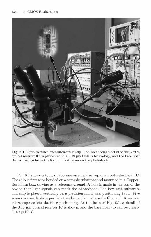
134 6 CMOS Realizations
Fig. 6.1. Opto-electrical measurement set-up. The inset shows a detail of the Gbit/soptical receiver IC implemented in a 0.18 µm CMOS technology, and the bare fiberthat is used to focus the 850 nm light beam on the photodiode.
Fig. 6.1 shows a typical labo measurement set-up of an opto-electrical IC.The chip is first wire-bonded on a ceramic substrate and mounted in a Copper-Beryllium box, serving as a reference ground. A hole is made in the top of thebox so that light signals can reach the photodiode. The box with substrateand chip is placed vertically on a precision multi-axis positioning table. Fivescrews are available to position the chip and/or rotate the fiber end. A verticalmicroscope assists the fiber positioning. At the inset of Fig. 6.1, a detail ofthe 0.18 µm optical receiver IC is shown, and the bare fiber tip can be clearlydistinguished.

6.2 Test Photodiodes with TIA in 0.18 µm CMOS 135
6.2 Test Photodiodes with TIA in 0.18 µm CMOS
As already mentioned in Section 4.5.1, the main purpose of this first chip isto compare the performance of different kind of photodiode topologies. TheTIA is the same for every photodiode. First the layout of the photodiodesand the design of the receiver circuit are discussed. This is followed by aninterpretation of the measurement results, of which the most successful onesare published in [Her04b, Her04c, Her06a].
6.2.1 Circuit Description
Photodiodes
The five test photodiodes are: a classical n-well diode, a quasi-fractal n-well diode, a differential n-well diode, a p+ n-well diode with guard andan n+ p-substrate diode. Their junction capacitances are respectively 660 fF,585 fF, 292 fF, 4.6 pF and 6.8 pF. All diodes have an area of 100x100 µm2.The layout of the classical n-well diode, the n+ p-substrate diode and thep+ n-well diode with guard is straightforward. They all have 10 square junc-tions per diode side (Ns in Sections 3.5.1 and 3.5.2), or 100 junctions in total.Between the junctions are substrate contacts to minimize the substrate resis-tance. The layout of the classical n-well diode is represented schematically inFig. 3.9. The layout of the n+ p-substrate diode is quasi the same, only then-well regions are replaced by n+ regions. The layout of the p+ n-well diodewith guard is represented schematically in Fig. 3.11. Every n-well square hastwo p+ regions surrounded by n-type contacts.
The layout of the two other diodes is slightly more complicated. The lay-out of the quasi-fractal n-well diode is based on a maximization of side-wallcapacitance, as this junction extends from the silicon surface down to thebottom of the n-well. A fractal is a well-known concept in mathematics andis defined as an object or quantity that displays self-similarity on all scales.The object repeated in the layout of the quasi-fractal topology (Fig. 6.2(a))is the n-well cross. As can be seen in the detail, the cross at the lowest levelhas eight extra branches on each side and the iterated pattern stops. Everyn-well junction is surrounded by substrate contacts to minimize its parasiticresistance.
The differential diode, depicted in Fig. 6.2(b), consists of an alternatingpattern of illuminated and dark junctions. Subtraction of these two signalscancels the slowly diffusing substrate carriers. The total number of junctionfingers (Nf in Section 3.5.3) equals 32. Measures have been taken to minimizesubstrate and contact resistance: every junction is surrounded by substratecontacts, every finger is divided into halves to provide extra substrate contactsand the junctions have additional connection stripes in horizontal direction.The covering metal used to block the light is metal 3, as metal 1 and metal 2were needed for routing.

136 6 CMOS Realizations
(a)
(b)
Fig. 6.2. Detailed layout of: (a) the quasi-fractal n-well diode, (b) the differentialn-well photodiode, both implemented in a 0.18 µm CMOS technology.
TIA and CSDA
Fig. 6.3 shows a schematic of the receiver. It consists of two identical tran-simpedance amplifiers (TIA1 and TIA2), a complementary self-biased differ-ential amplifier (CSDA) [Baz91, Pie04] and an output buffer to drive the 50Ωload. For the differential photodiode, diode PD1 corresponds to the illumi-nated junctions, while diode PD2 corresponds to the dark junctions. The slow

6.2 Test Photodiodes with TIA in 0.18 µm CMOS 137
nbias
PD1
CSDA
TIA1 TIA2
tooutputbuffer
Vdd
R f2f1 R
1M
2M 4M
3M
PD2
1aM 1bM
2aM 2bM
2cM
1cM
Fig. 6.3. Simplified schematic of the 0.18 µm CMOS receiver circuit, needed toamplify the currents generated by the test photodiodes.
diffusion carriers detected by the two diodes appear as a common-mode sig-nal at the two inputs of the CSDA and are suppressed. Only the fast currentcomponent, which is mainly the drift current, is then amplified. For the othertopologies, diode PD1 is the one that captures the signal, while diode PD2 isa dummy diode placed for biasing and matching.
The design of the TIA has been discussed thoroughly in Section 4.5.1. Asthe measurements always have been performed with Vb2=1.8 V, transistorsM3, M1d and M2d shown in Fig. 4.7(a) are left out in the simplified schematicdepicted in Fig. 6.3.
The CSDA consists of two complementary differential stages, from whichthe loads have been removed. Transistors M1a, M1b and M1c make up then-type half, while transistors M2a, M2b and M2c make up the p-type half.The gates of two complementary input transistors are connected so that theinput stage is now an inverter. The transconductance is approximately dou-bled compared to the transconductance of a conventional differential stage. Inorder to create a stable current through biasing transistors M1c and M2c, noexternal voltage is applied, but their gates are connected to the internal am-plifier node nbias. This self-biasing of the amplifier creates a negative feedbackloop that stabilizes the bias voltages and makes it less sensitive to process ortemperature variations. Because the voltage at nbias equals about one halfof the power supply, transistors M1c and M2c operate in the linear region.Consequently, the voltages at their drains may be set very close to the supplyvoltages. So the output swing of this amplifier approaches the power supply.Table 6.1 summarizes the design parameters of the CSDA.

138 6 CMOS Realizations
Table 6.1. Design parameters of the complementary self-biased differential amplifier(CSDA).
M1a/M1b M2a/M2c M1c M2c
type nMOS pMOS nMOS pMOS
L 0.18 µm 0.18 µm 0.18 µm 0.18 µm
W 40 µm 80 µm 40 µm 80 µm
VDSAT 0.17 V 0.25 V 0.26 V 0.26 V
IDS 1.2 mA 1.2 mA 2.4 mA 2.4 mA
gm 11 mS 9.1 mS 7.7 mS 7.2 mS
gds 0.5 mS 0.4 mS 12 mS 5.1 mS
Cgs 47 fF 99 fF 44 fF 99 fF
Cgd 15 fF 28 fF 26 fF 37 fF
The single-ended output of the CSDA is connected to the output buffer. Itis realized as a single-stage inverter with an nMOS diode load to control theDC threshold voltage. This last stage consumes 1.4 mA from the 1.8 V supplyvoltage. Finally, a major advantage of this receiver topology is that TIA,CSDA as well as the output buffer all have a CMOS inverter topology, whichmakes it very suitable to implement in standard digital CMOS technologies.
6.2.2 Measurements
All test photodiodes are integrated with the amplifier stages in a standard0.18 µm 1.8 V CMOS technology. No additional masks are used to enhancethe performance of the photodiodes. On top of the diodes, there is only thestandard dielectric stack, no anti-reflective coating. The chip photograph isdepicted in Fig. 6.4. The total chip area taken by the five receivers, includingbond pads and decoupling capacitors, equals 1x3.6 mm2. Every photodiode isfollowed by an identical amplifying circuit that consumes only 17 mW.
The optical source used during measurements is a commercially available850 nm Infineon transmitter. The average optical power is −6 dBm, and forsensitivity measurements this signal is attenuated by an EXFO attenuator.The electrical 27-1 prbs data stream is generated by the HP data generator.The eye diagrams are constructed by triggering the Tektronix oscilloscope andby applying a display setting of infinite persistence. BER and jitter measure-ments are obtained from the SyntheSys BitAlyzer.
Fig. 6.5 compares the eye diagrams of the test diodes at 300 Mbit/s. A 27-1prbs data stream with an average input optical power (Popt) of −7 dBm isapplied. The slowly rising tail originating from the diffusing substrate carrierscan be clearly distinguished in the eye diagram of the classical n-well diode(Fig. 6.5(a)). The eye quality of the quasi-fractal n-well diode (Fig. 6.5(b)) isslightly better, as relatively more carriers are generated now in the side-wall

6.2 Test Photodiodes with TIA in 0.18 µm CMOS 139
Fig. 6.4. Chip photograph of the five testdiodes with amplifying circuit in 0.18 µmstandard CMOS.
(a) (b)
(c) (d)
Fig. 6.5. Eye diagrams of the 0.18 µm test diodes with amplifying circuit. The inputsignal has a bitrate of 300 Mbit/s and Popt=−7 dBm. The different diodes are: (a)classical n-well diode, (b) quasi-fractal n-well diode, (c) p+ n-well diode with guard,(d) differential n-well diode.
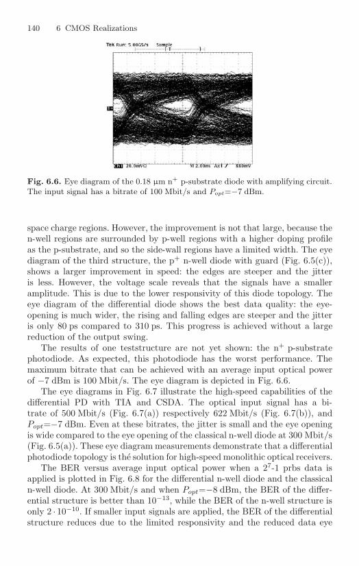
140 6 CMOS Realizations
Fig. 6.6. Eye diagram of the 0.18 µm n+ p-substrate diode with amplifying circuit.The input signal has a bitrate of 100 Mbit/s and Popt=−7 dBm.
space charge regions. However, the improvement is not that large, because then-well regions are surrounded by p-well regions with a higher doping profileas the p-substrate, and so the side-wall regions have a limited width. The eyediagram of the third structure, the p+ n-well diode with guard (Fig. 6.5(c)),shows a larger improvement in speed: the edges are steeper and the jitteris less. However, the voltage scale reveals that the signals have a smalleramplitude. This is due to the lower responsivity of this diode topology. Theeye diagram of the differential diode shows the best data quality: the eye-opening is much wider, the rising and falling edges are steeper and the jitteris only 80 ps compared to 310 ps. This progress is achieved without a largereduction of the output swing.
The results of one teststructure are not yet shown: the n+ p-substratephotodiode. As expected, this photodiode has the worst performance. Themaximum bitrate that can be achieved with an average input optical powerof −7 dBm is 100 Mbit/s. The eye diagram is depicted in Fig. 6.6.
The eye diagrams in Fig. 6.7 illustrate the high-speed capabilities of thedifferential PD with TIA and CSDA. The optical input signal has a bi-trate of 500 Mbit/s (Fig. 6.7(a)) respectively 622 Mbit/s (Fig. 6.7(b)), andPopt=−7 dBm. Even at these bitrates, the jitter is small and the eye openingis wide compared to the eye opening of the classical n-well diode at 300 Mbit/s(Fig. 6.5(a)). These eye diagram measurements demonstrate that a differentialphotodiode topology is the solution for high-speed monolithic optical receivers.
The BER versus average input optical power when a 27-1 prbs data isapplied is plotted in Fig. 6.8 for the differential n-well diode and the classicaln-well diode. At 300 Mbit/s and when Popt=−8 dBm, the BER of the differ-ential structure is better than 10−13, while the BER of the n-well structure isonly 2 · 10−10. If smaller input signals are applied, the BER of the differentialstructure reduces due to the limited responsivity and the reduced data eye

6.2 Test Photodiodes with TIA in 0.18 µm CMOS 141
(a) (b)
Fig. 6.7. High-speed eye diagrams of the 0.18 µm differential n-well diode withamplifying circuit. Popt=−7 dBm and the bitrate equals: (a) 500 Mbit/s, (b)622 Mbit/s.
−12 −11 −10 −9 −8 −710
−18
10−15
10−12
10−9
10−6
10−3
Average input power [dBm]
bit e
rror
rat
e
classical n−well diode, 300Mbit/sdifferential n−well diode, 300Mbit/sdifferential n−well diode, 500Mbit/s
Fig. 6.8. Bit error rate versus average input power of the 0.18 µm classical anddifferential n-well photodiode with amplifying circuit.
width. At 500 Mbit/s, the differential n-well diode achieves a BER of 3 · 10−10
when an input optical signal of −8 dBm is applied.The frequency response of the differential n-well diode followed by TIA,
CSDA and output buffer, is depicted in Fig. 6.9. A Rohde&Schwarz networkanalyzer is used to modulate the laser driver and to evaluate the electricaloutput signal of the receiver. Measurements are done for the maximum andminimum value of the feedback resistance. When the transimpedance gain ishigh, the 3-dB bandwidth is 177 MHz. When the transimpedance gain is low,the 3-dB bandwidth is 245 MHz. So bandwidth is inversely proportional to

142 6 CMOS Realizations
108
109
−70
−60
−50
−40
−30
−20
−10
frequency [Hz]
Out
put p
ower
[dB
m]
ZTIA
=65 dBΩ
ZTIA
=54 dBΩ
Fig. 6.9. Frequency response of the 0.18 µm differential n-well photodiode followedby TIA, CSDA and output buffer.
Table 6.2. Performance summary of the classical and differential n-well photodiodewith amplifying circuit in 0.18 µm CMOS.
Classical Differential
n-well diode n-well diode
Technology 0.18 µm CMOS
Vdd 1.8 V
Optical wavelength 850 nm
Die area 1000x685 µm2 1000x565 µm2
Bitrate 300 Mbit/s 500 Mbit/s
BER@Popt=−8 dBm 2 · 10−10 3 · 10−10
rms jitter@Popt=−7 dBm 310 ps 80 ps
Power dissipation 17 mW
transimpedance gain, as described by (4.11). The 3-dB bandwidth is howeversmaller than the values predicted by the TIA-simulations in Section 4.5.1.This is due to the lower intrinsic bandwidth of the differential diode, andproves that the diode is the speed limiting component. The measurementresults of both the classical and the differential n-well diode are summarizedin Table 6.2.
6.3 Test Photodiodes with TIA in 90 nm CMOS
The objective of this chip is very similar to the objective of the chip discussedin the previous section (Section 6.2): the comparison of the performance of
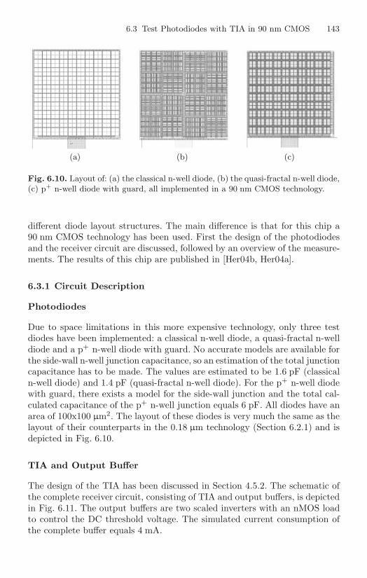
6.3 Test Photodiodes with TIA in 90 nm CMOS 143
(a) (b) (c)
Fig. 6.10. Layout of: (a) the classical n-well diode, (b) the quasi-fractal n-well diode,(c) p+ n-well diode with guard, all implemented in a 90 nm CMOS technology.
different diode layout structures. The main difference is that for this chip a90 nm CMOS technology has been used. First the design of the photodiodesand the receiver circuit are discussed, followed by an overview of the measure-ments. The results of this chip are published in [Her04b, Her04a].
6.3.1 Circuit Description
Photodiodes
Due to space limitations in this more expensive technology, only three testdiodes have been implemented: a classical n-well diode, a quasi-fractal n-welldiode and a p+ n-well diode with guard. No accurate models are available forthe side-wall n-well junction capacitance, so an estimation of the total junctioncapacitance has to be made. The values are estimated to be 1.6 pF (classicaln-well diode) and 1.4 pF (quasi-fractal n-well diode). For the p+ n-well diodewith guard, there exists a model for the side-wall junction and the total cal-culated capacitance of the p+ n-well junction equals 6 pF. All diodes have anarea of 100x100 µm2. The layout of these diodes is very much the same as thelayout of their counterparts in the 0.18 µm technology (Section 6.2.1) and isdepicted in Fig. 6.10.
TIA and Output Buffer
The design of the TIA has been discussed in Section 4.5.2. The schematic ofthe complete receiver circuit, consisting of TIA and output buffers, is depictedin Fig. 6.11. The output buffers are two scaled inverters with an nMOS loadto control the DC threshold voltage. The simulated current consumption ofthe complete buffer equals 4 mA.

144 6 CMOS Realizations
M1
M2
M3b2V
Cac
Rfb
MRfb
b1V
Mb2
ddV
Mb1 Mb3 Mb4 Mb6
Mb5
Photodiode and TIA Output Buffer
to 50 Ohm
Fig. 6.11. Schematic of the 90 nm receiver circuit, needed to amplify the currentsgenerated by the test photodiodes.
6.3.2 Measurements
Fig. 6.12 shows a photograph of the 90 nm CMOS test chip. The upper partcontains two stand-alone test diodes: the classical n-well diode and the quasi-fractal n-well diode. Both diodes are also implemented with the amplifyingcircuit (TIA and output buffer). In the lower part, the same structures are re-peated for the p+ n-well diode with guard. The area of the upper part equals1000x800 µm2, the area of the lower part equals 450x1000 µm2. No additionalmasks or anti-reflective coatings are used to enhance the performance of thephotodiodes. As already mentioned in Section 4.5.2, no MiM-capacitors wereavailable. To achieve a high capacitance density both for the on-chip decou-pling and for Cac (Fig. 6.11), the metal wall structure is used [Yao04]. Itcreates a large capacitance value on a small area by using the side-wall ca-pacitance of 8 metals from the 9 metal layer stack. With a supply voltage of1.1 V, the amplifying circuit consumes 9 mW. The measurement set-up is thesame as for the 0.18 µm test diodes. The only difference is that to determinethe BER, the Agilent’s Infinium oscilloscope has been used, that calculatesthe BER out of Q-factor measurements.
The stand-alone testdiodes have been used to measure the DC responsivity.The n-well diode has a responsivity of 0.3 A/W, while the p+ n-well diode withguard has a responsivity of only 0.006 A/W.
Fig. 6.13 shows the eye diagrams when a 232-1 prbs at a bitrate of100 Mbit/s and with an average input optical power (Popt) of −7 dBm isapplied. The eye diagram of the front-end with the n-well diode (Fig. 6.13(a))clearly shows the slowly rising tail originating from the diffusing carriers inthe substrate. There is not much difference between the eye diagram of thequasi-fractal n-well diode (Fig. 6.13(b)) and the classical n-well diode. Theimprovement is much less when compared with the 0.18 µm test structures.This is probably due to the higher doping concentration of the p-well. As a

6.3 Test Photodiodes with TIA in 90 nm CMOS 145
Fig. 6.12. Chip photograph of the three testdiodes with amplifying circuit in 90 nmstandard CMOS.
result, the width of the depletion region is smaller, and the contribution ofthe drift current to the total current decreases. This explains why there is notmuch improvement in speed by optimizing the sidewall capacitance using aquasi-fractal structure. At the other hand, the eye diagram of the front-endwith the p+ n-well diode with guard (Fig. 6.13(c)) is much better: the eye-opening is wider and the rising/falling edges are steeper. This demonstratesthat the diffusing carriers are effectively removed by the substrate contacts.In Fig. 6.14(a) and Fig. 6.14(b), two high-speed eye diagrams at 400 Mbit/sand 500 Mbit/s respectively of the p+ n-well diode with guard and amplifyingcircuit are shown.
To perform sensitivity measurements, the output signals are amplified witha Mini-Circuits broadband low-noise amplifier (LNA). Its low-frequency cut-off equals 1 kHz and its upper 3-dB bandwidth equals 1 GHz. The LNA isfurther characterized by a gain of 20 dB and a noise figure of 3 dB. Sensitivityof the two front-ends is determined by applying a 232-1 prbs and by measuringthe Q-factor of the output data after the LNA. The optical attenuation be-tween the optical source and the device under test has been adjusted to obtaina Q-factor of 6. This value corresponds to a BER of 10−9. At 100 Mbit/s, thefront-end with n-well diode has a sensitivity of −9 dBm, while the front-end

146 6 CMOS Realizations
(a) (b)
(c)
Fig. 6.13. Eye diagrams of the 90 nm test diodes with amplifying circuit. The inputsignal has a bitrate of 100 Mbit/s and Popt=−7 dBm. The different diodes are: (a)classical n-well diode, (b) quasi-fractal n-well diode, (c) p+ n-well diode with guard.
with the quasi-fractal n-well diode has a sensitivity of −8.3 dBm. The front-end with p+ n-well diode with guard even achieves a sensitivity of −10.4 dBmat 400 Mbit/s, and a sensitivity of −8 dBm at 500 Mbit/s. All measurementsare summarized in Table 6.3.
6.4 A 3.5 Gbit/s LA in 0.18 µm CMOS
After two chips with photodiodes and TIAs, a CMOS implementation of thenext receiver building block is presented: the limiting amplifier. Again, anoverview of the circuit topology is given before the measurements are dis-cussed. The results are also published in [Her05, Her06a].

6.4 A 3.5 Gbit/s LA in 0.18 µm CMOS 147
(a) (b)
Fig. 6.14. High-speed eye diagrams of the p+ n-well diode with guard and ampli-fying circuit. Popt=−7 dBm and the bitrate equals: (a) 400 Mbit/s, (b) 500 Mbit/s.
Table 6.3. Performance summary of the test photodiodes with amplifying circuitin 90 nm CMOS.
TIA with TIA with quasi- TIA with p+ n-well
n-well diode fractal n-well diode diode with guard
Technology 90 nm standard CMOS
Vdd 1.1 V
Optical wavelength 850 nm
Die area 450x800 µm2 450x800 µm2 450x1000 µm2
Diode responsivity 0.3 A/W - 0.006 A/W
Bitrate 100 Mbit/s 100 Mbit/s 400 Mbit/s
500 Mbit/s
Sensitivity −9 dBm −8.3 dBm −10.4 dBm
@BER=10−9 −8 dBm
Power dissipation 9 mW
6.4.1 Circuit Description
Four-Stage Limiting Amplifier
The design of this LA has been discussed previously in Section 5.5.1. The LAconsists of four cascaded Cherry-Hooper stages, as depicted in Fig. 5.5.
Output Buffer
The output buffer, necessary to drive the 50 Ω of the measurement equipment,consists of two stages. To achieve a broad bandwidth, each stage comprises

148 6 CMOS Realizations
Vdd
I1
Vin2
Vb
M1 M2 M4M3
Vout1 Vout2
Mc1 Mc3Mc2
Rl Rl
m*g v/4 m*g v/4
m*g v/4* R*2 lm*g v/4* R*2 l
v/20
nA nB
v/2
in1V
Fig. 6.15. Schematic of the fT -doubler.
an fT -doubler [Raz02], shown in Fig. 6.15. Transistors M1 to M4 all havethe same sizing (W = 40 µm in the first stage and W = 80 µm in the secondstage) and operating point (Ids = 2 mA in the first stage and Ids = 7 mA inthe second stage, all lengths are chosen minimal). Resistor Rl is the load oftransistors M1 and M3 at one side, and transistors M2 and M4 at the otherside. Compared to a traditional differential pair with resistive load, this circuitreduces the input capacitance while maintaining the same gain.
Consider a differential voltage v applied at the input transistors M1 andM4. The small signal behavior of the circuit is also shown in Fig. 6.15. Theinput Vin1 goes up with an amplitude of v/2, while the input Vin2 goes downwith the same amplitude. Vb is zero, as it is a bias voltage equal to the common-mode level of Vin1 and Vin2. As a consequence, a current equal to gmv/4 flowsfrom drain to source in transistors M1 and M3, and from source to drain intransistors M2 and M4. These currents add up at the output nodes whichresults in a negative small-signal voltage 2 · gmv/4Rl at Vout1 and a posi-tive small-signal voltage 2 · gmv/4Rl at Vout2. So the differential gain equalsgmRl, which is the same as that of a differential pair with input transistortransconductance gm and load resistor Rl.
By using the configuration of Fig. 6.15, the input ports of the transistorsare placed in series while the output ports are connected in parallel. Thisresults in a lower input capacitance. If the parasitic capacitance at the twocommon-mode nodes nA and nB is negligible, the input capacitance is roughlyequal to Cgs/2, where Cgs is the gate-source capacitance of transistors M1 toM4 Hence the name fT -doubler: the circuit halves the input capacitance whilemaintaining the same overall transconductance.
The circuit also suffers from several drawbacks compared to a simple dif-ferential pair. First, the power dissipation is doubled. Next, the total currentflowing through the load resistors is doubled, making it more difficult to keepthe transistors in saturation. Further, the total output capacitance is doubled.

6.4 A 3.5 Gbit/s LA in 0.18 µm CMOS 149
Fig. 6.16. Chip photograph of the 3.5 Gbit/s LA in 0.18 µm standard CMOS.
Finally, if the parasitic capacitance at nodes nA and nB is not negligible, theinput capacitance is higher than Cgs/2.
6.4.2 Measurements
A die photograph of the limiting amplifier with output buffer is depicted inFig. 6.16. A standard 0.18 µm 1.8 V CMOS technology is used for the imple-mentation. Total chip area including bond pads and decoupling capacitors is1.3x1.5 mm2. Special attention has been paid to make the layout symmetri-cal, both for the differential stages in the LA and for the differential stagesin the buffer. The power dissipation equals 70 mA, from which only 19 mA isconsumed by the LA.
Bit error rate (BER), eye diagram and jitter measurements are obtainedfrom the Agilent ParBERT (Parallel Bit Error Ratio Tester). A differential231-1 prbs is applied at the input. Fig. 6.17 and Fig. 6.18 show eye diagramsat 1 Gbit/s and at 3.5 Gbit/s respectively, and for different input amplitudes.The eye opening measurement obtained from the ParBERT generates a three-dimensional bit error rate diagram as a function of the sample delay (x-axis)and the sample threshold (y-axis). The contour of the eye is derived from thebit error rates that have been measured. Different grey-levels are used for theregions between the lines of equal bit error rate: black corresponds to a BERlower than 10−12. The eye opening is the best for large input signals and lowbit-rates. But even for an input signal with a bitrate of 3.5 Gbit/s and aninput voltage of 10 mVpp, the eye is still considerably open.

150 6 CMOS Realizations
(a)
(b)
Fig. 6.17. Eye diagrams at 1 Gbit/s of the four-stage LA with output buffer:(a) Vin = 100 mVpp, (b) Vin = 10 mVpp.
(a)
(b)
Fig. 6.18. Eye diagrams at 3.5 Gbit/s of the four-stage LA with output buffer:(a) Vin = 100 mVpp, (b) Vin = 10 mVpp.

6.4 A 3.5 Gbit/s LA in 0.18 µm CMOS 151
1 2 3 410
−14
10−13
10−12
10−11
bitrate [Gbit/s]
bit e
rror
rat
e
Fig. 6.19. Bit error rate versus bitrate of the four-stage LA with output buffer.The input prbs signal has an amplitude of 10 mVpp.
Table 6.4. Performance summary of the 3.5 Gbit/s 0.18 µm LA.
Technology 0.18 µm CMOS
Vdd 1.8 V
Differential gain 27 dB
Bitrate 3.5 Gbit/s
BER@10 mVpp 5 · 10−12
rms jitter 12 ps
Power dissipation 70 mA (LA: 19 mA)
The results of the bit error rate tests are shown in Fig. 6.19. A differen-tial 231-1 prbs input signal with an amplitude of 10 mVpp is applied, whilefor each test the bitrate of the input is changed. As expected, the higherthe bitrate, the higher the bit error rate. At 1 Gbit/s the BER is as low as7 · 10−14, while at 3.5 Gbit/s the BER is still only 5 · 10−12. The rms jitter isslightly dependent on level and speed of the input signal. For an input level of10 mVpp and a bitrate of 3.5 Gbit/s, the measured rms jitter is 16 ps. Takingthe rms jitter added by the ParBERT into account, the post-amplifier andbuffer establish an rms jitter of only 12 ps. Finally, the small-signal voltagegain is measured with a network analyzer. This results in a measured single-ended voltage gain of 21 dB, which corresponds to a differential voltage gainof 27 dB. The measurement results are summarized in Table 6.4.
In Table 6.8 at the end of this chapter, the performance of this LA [Her05]is compared with the papers discussed in Section 5.3. First it is noticed thatthe BiCMOS implementations achieve gain-bandwidth products larger thanone 1 THz with 20-year-old technologies. Comparing [Her05] with the 0.18 µm
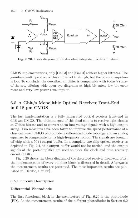
152 6 CMOS Realizations
PA outV
Vbias
Vbias
blockR
fblockR
C
blockC
block
f
withNIC
50 Ohm
CH
R
A Equalizer
R
buffer
50 Ohm
Fig. 6.20. Block diagram of the described integrated receiver front-end.
CMOS implementations, only [Gal03] and [Gal04] achieve higher bitrates. Thegain-bandwidth product of this chip is not that high, but the power dissipationis low. To conclude, the described amplifier is comparable with today’s state-of-the-art, offering wide-open eye diagrams at high bit-rates, low bit errorrates and very low power consumption.
6.5 A Gbit/s Monolithic Optical Receiver Front-Endin 0.18 µm CMOS
The last implementation is a fully integrated optical receiver front-end in0.18 µm CMOS. The ultimate goal of this final chip is to receive light signalsat Gbit/s bitrate and to convert them into voltage signals with a high outputswing. Two measures have been taken to improve the speed performance of aclassical n-well CMOS photodiode: a differential diode topology and an analogequalizer to compensate for its high-frequency roll-off. The signals are broughtoff-chip with a 50 Ω output buffer. In a complete one-chip optical receiver asdepicted in Fig. 2.1, this output buffer would not be needed, and the outputsignals of the post-amplifier are used to steer the clock and data recoverycircuit (CDR).
Fig. 6.20 shows the block diagram of the described receiver front-end. Firstthe implementation of every building block is discussed in detail. Afterwardsthe measurement results are presented. The most important results are pub-lished in [Her06c, Her06b].
6.5.1 Circuit Description
Differential Photodiode
The first functional block in the architecture of Fig. 6.20 is the photodiode(PD). As the measurement results of the different photodiodes in Section 6.2

6.5 A Gbit/s Monolithic Optical Receiver Front-End in 0.18 µm CMOS 153
Fig. 6.21. Photo of the 0.18 µm CMOS differential photodiode.
demonstrate the superiority of the differential photodiode concerning elimi-nation of substrate carriers, also a differential PD is chosen for the presentedreceiver.
Fig 6.21 depicts a photo of the implemented CMOS PD. As the core andcladding of the fiber are circular, an octagonal form is taken with a diagonalof 80 µm. The PD consists of 18 fingers, of which 9 are covered with metal.To minimize optical non-idealities, this covering metal should be located asclose to the silicon surface as possible. As metal 1 is used for routing, metal 2is used for this purpose. Between the junction fingers, substrate contacts areforeseen to minimize substrate resistance. For the same reason, every fingeris cut in two in the middle to place extra substrate contacts. The diode isalso surrounded by a broad guard ring of substrate contracts. The junctioncapacitance of the illuminated PD as well as the dark PD, with a reversevoltage of 1.3 V, equals 159 fF.
Differential Transimpedance Amplifier
Before subtraction of the PD signals, the currents from the illuminated PDand dark PD are first converted into a voltage by a differential TIA. The designof this circuit has been elaborated in detail in Section 4.5.3. The schematic ofthis differential TIA is depicted in Fig. 4.12.
A high-pass filter, consisting of Cblock and Rblock, is needed to set theDC-level at the input of the subsequent differential stages. The major reasonis that the signals from the illuminated and dark junctions have a differentpeak-to-peak value, and thus generate different DC-levels at the output of theTIA. This is not optimal for correct differential operation. Therefore, the biasvoltage Vbias is applied externally and data-independent. The values of Cblock
and Rblock must be chosen carefully, as too small values create a relativelyhigh 3-dB frequency. As a result, lower frequency components in the prbsdata stream are considered as DC-voltage variations and filtered out. This

154 6 CMOS Realizations
baseline wander must be avoided. In the current design, Cblock=2 pF andRblock=20 kΩ, which gives a 3-dB frequency of 4 MHz.
Subtraction Block
Now the currents of the PDs have been converted into voltages, their differ-ence can be made by a differential voltage amplifier. The signal originatingfrom the diffusing substrate carriers will appear as a common-mode signalat the input of this amplifier and will be suppressed. This function is im-plemented by a modified Cherry-Hooper topology with negative impedanceconverter to enhance bandwidth. The design of this stage has been explainedin Section 5.5.2, where is was used as one of the amplifying stages in the lim-iting amplifier. The specifications of this block are however slightly different.In the subtraction block, it can be important to make a differential signal in-troducing as little non-idealities as possible, so bandwidth is maximized. Alsothe common-mode suppression should be high for a wide frequency band.
Simulations show a bandwidth of 5 GHz when this stage is loaded with thealmost 200 fF input capacitance of the equalizer. The small-signal differentialgain equals 6 dB.
Equalizer
The function of the equalizer is to compensate for the frequency roll-of ofthe differential diode. Therefore, equalization is performed after subtractionof the signals. The advantage of equalizing a differential PD compared to aclassical n-well diode [Rad04, Rad05] is the intrinsic potential of a better speedperformance. The price to pay is a lower sensitivity.
The design of this block has been the subject of a master’s thesis [Tav05,Tav06]. The circuit diagram of the equalizer is presented in Fig. 6.22(a) andthe design parameters are summarized in Table 6.5. It is a pseudo-differentialstage, with second-order capacitive source degeneration to create zeros at thedesired frequencies. Its transfer function is given by:
Geq = − gm,M1Rx
1 + gm,M1R1Z2Z3
R1Z2+R1Z3+Z2Z3
. (6.1)
Using the expressions for Z2 and Z3:
Z2 = R2 +1
sC2, (6.2)
Z3 = R3 +1
sC3, (6.3)
and assuming that gm,M1R1 is sufficiently large, the transfer function reducesto:

6.5 A Gbit/s Monolithic Optical Receiver Front-End in 0.18 µm CMOS 155
2
C2
R1R3
C3
R1R2
C2 C3
R3
M1aVin1 Vin2M1b
Rx Rx
R
Vout1
Vdd
nxbnxa
n1a n1b
Vout2
(a)
106
107
108
109
−10
−5
0
5
10
frequency [Hz]
gain
[dB
]
EqualizerPDCompensated PD
(b)
Fig. 6.22. The analog equalizer: (a) schematic, (b) uncompensated and compen-sated characteristics of the differential photodiode (PD).
Geq = −Rx
R1
s2R2C2C3 + s((R1 + R2)C2 + (R1 + R3)C3) + 1s2R2R3C2C3 + s(R2C2 + R3C3) + 1
, (6.4)
with:R2 = R1R2 + R2R3 + R1R3. (6.5)
To gain intuitive insight, it is assumed that the different poles are well sepa-rated (which is not necessarily true in a practical implementation), and (6.4)than further becomes:
Geq = −Rx
R1
(1 + s(R1 + R2)C2)(1 + s(R1 + R3)C3)(1 + sR2C2)(1 + sR3C3)
. (6.6)
The gain is determined by the ratio Rx/R1. Adding a branch with resistorR and capacitor C creates a zero at frequency 1/2π(R1 + R)C and a pole atfrequency 1/2πRC.

156 6 CMOS Realizations
Table 6.5. Design parameters of the analog equalizer.
M1
type nMOS
L 0.18 µm
W 107 µm
VDSAT 0.21 V
IDS 6.1 mA
gm 38 mS
gds 1.7 mS
Cgs 128 fF
Cgd 39 fF
Rx 87 Ω
R1 48 Ω
R2 89 Ω
R3 0 Ω
C1 3.7 pF
C1 2 pF
Fig. 6.22(b) illustrates the working principle of the equalizer. As derivedin Section 3.5.3, the transfer characteristic of a differential PD with 18 fingershas a 3-dB frequency of 1 GHz and a roll-off increasing from 3 dB/decade upto 10 dB/decade above 1 GHz. The Eldo-simulations of the equalizer show acorresponding roll-up. The result is a compensated diode characteristic thatis almost flat up to 5 GHz.
Five-Stage Limiting Amplifier
The block diagram of the LA is depicted in Fig. 5.9. Its design has beenstudied thoroughly in Section 5.5.2.
Output Buffer
The output buffer is needed to drive the off-chip 50 Ω load. It consists offour scaled stages: three fT -doublers (discussed in Section 6.4.1 and depictedin Fig. 6.15) and one differential pair with resistive load. For the last stage,a simple differential pair is preferred over the fT -doubler, as the latter oneincreases the output capacitance, and the output load is already assumed tobe 1 pF. Each stage has a larger input transistor (from 24 µm up to 232 µm),consequently a higher input capacitance, also a higher current consumptionand a lower load resistance (from 250 Ω down to 40 Ω parallel with 50 Ω).Note also that for this output buffer the small-signal 3-dB bandwidth is not

6.5 A Gbit/s Monolithic Optical Receiver Front-End in 0.18 µm CMOS 157
Fig. 6.23. Chip photograph of the Gbit/s monolithic optical receiver in 0.18 µmstandard CMOS.
a good measure for its speed performance, as signals with a high amplitudeare generated by the LA. Usually, the small-signal bandwidth is a lower limit,but transient signals simulations have to be performed too.
Large and high-speed output signals result in a high power consumption:this block consumes 170 mA from the 1.8 V power supply. The on-chip voltageswing of 1.2 Vpp at the output of the LA is converted into a simulated 50 Ωoff-chip swing of 500 mVpp, at bitrates up to 6 Gbit/s.
6.5.2 Measurements
A chip photograph of the receiver with photodiode, integrated in a 0.18 µm1.8 V CMOS technology, is depicted in Fig. 6.23. Die area, including bond padsand on-chip decoupling, is 1.5x3 mm2. No additional masks or anti-reflectivecoatings have been used to enhance the optical performance of the diode. Themeasured photodiode DC responsivity for the differential signal is 0.03 A/W.The current consumption of the complete front-end is 250 mA. Both the TIAand LA consume 40 mA each, 170 mA is dissipated in the output buffer togenerate high-speed 500 mVpp signals off-chip. The measurement results aresummarized in Table 6.6. In the following, first the measurements for the LAwith output buffer are shown. Next the performance of the complete front-endis discussed.
Limiting Amplifier with Output Buffer
Bit error rate (BER), eye diagram and jitter measurements are obtainedfrom the Agilent ParBERT (Parallel Bit Error Ratio Tester). Applying a 27-1

158 6 CMOS Realizations
prbs, error free operation from 800 Mbit/s up to 6 Gbit/s has been measured.The rms jitter equals 8 ps. The BER measurements versus input voltage at4 Gbit/s, 5 Gbit/s and 6 Gbit/s are summarized in Fig. 6.24(a). At 6 Gbit/s,an input voltage of 8 mVpp is needed to achieve a BER of 10−12. The cor-responding eye diagram is depicted in Fig. 6.25(a). The smaller the inputamplitude, the higher the bit error rate: a 6 mVpp input voltage at 6 Gbit/sresults in a BER of 10−9. At 5 Gbit/s and 4 Gbit/s , the sensitivity for aBER of 10−12 is 5 mVpp respectively 3 mVpp. Due to clipping of the firstCherry-Hooper stage, the limiting amplifier is also capable of handling verylarge signals. The input swing is only limited by the maximum tolerable volt-age at the input, that has to be smaller than the supply voltage for reliabilityreasons. When the input voltage is 600 mVpp, the BER is better than 10−13,independent of the bitrate. For a bitrate of 6 Gbit/s, the eye diagram is shownin Fig. 6.25(b). This results in a dynamic range with BER< 10−12 of 37.5 dBat 6 Gbit/s , 41.5 dB at 5 Gbit/s and 46 dB at 4 Gbit/s.
Table 6.8 compares the performance of this LA [Her06c] with present state-of-the art. The amplifier achieves a higher gain-bandwidth product than mostother 0.18 µm CMOS LAs. Only [Gal03], which uses integrated passive induc-tors to increase the bandwidth, has an extremely high gain-bandwidth prod-uct. Furthermore, the power dissipation of the latter is higher than in [Her06c].The high gain-bandwidth product of this LA results in maximal achievablebitrates with a low BER as high as 6 Gbit/s, combined with a high gain, ahigh input dynamic range and a high output swing.
Optical Receiver
The optical measurements of the complete receiver are performed with a com-mercially available 850 nm Agilent transmitter, electrically driven with a 27-1prbs generated by the ParBERT. The average output power of the trans-mitter is −6 dBm, and for sensitivity measurements this signal is attenuatedby an EXFO attenuator. The BER measurements for bitrates ranging from1 Gbit/s to 1.9 Gbit/s are summarized in Fig. 6.24(b). The BER becomesworse for higher bitrates and lower input powers. At 1.7 Gbit/s, −6 dBm isneeded to achieve a BER smaller than 10−12. The eye diagram of this outputsignal is shown in Fig. 6.26(b). For comparison, a 1 Gbit/s eye diagram isshown in Fig. 6.26(a) that achieves a BER< 10−14. The jitter, characterizedby an rms value of 35 ps, is clearly visible in these eyes and is the bottleneckfor achieving higher bitrates.
Much effort has been put in finding out where the jitter originates from.After all, purely electrical measurements demonstrate that the circuit, fromTIA to output buffer, performs according to expectations. Fig. 6.27 shows eyediagrams when the TIA is driven by an electrical 27-1 prbs signal from theParBERT with an amplitude of 4 mVpp, corresponding to an equivalent inputcurrent of 8 µApp. Taking a responsivity of 0.03 A/W into account, this wouldcorrespond to an average input optical power of 133 µW, or −8.75 dBm. The

6.5 A Gbit/s Monolithic Optical Receiver Front-End in 0.18 µm CMOS 159
2 4 6 810
−13
10−12
10−11
10−10
10−9
peak−to−peak input voltage (mVpp
)
bit e
rror
rat
e
6 Gbit/s5 Gbit/s4 Gbit/s
(a)
−12 −11 −10 −9 −8 −7 −6 −510
−14
10−12
10−10
10−8
10−6
average input power (dBm)
bit e
rror
rat
e
1.9 Gbit/s1.8 Gbit/s1.7 Gbit/s1.5 Gbit/s1 Gbit/s
(b)
Fig. 6.24. Bit error rate measurements: (a) BER of the five-stage LA with outputbuffer versus input voltage for different bitrates, (b) BER of the Gbit/s opticalreceiver versus average input optical power for different bitrates.
comparison of Fig. 6.26(a) and Fig. 6.27(a) shows that the jitter is much lesswhen a pure electrical input signal is applied. The 5 Gbit/s eye depicted inFig. 6.27(b) shows that the data quality now degrades due to bandwidth lim-itations (as expected at this speed) and not due to jitter limitations. BERtests of the 5 Gbit/s eye result in a BER smaller than 10−14. The importantdifference with the optical measurements is that the eyes in Fig. 6.27 are mea-sured with a purely differential signal at the input. The nature of the signalsgenerated by the differential photodiode is totally different: the signals fromthe illuminated and dark photodiode have the same polarity, but different am-plitudes, and thus a common-mode component. Following experiments havebeen performed with electrical signals of the same polarity at the input:

160 6 CMOS Realizations
(a)
(b)
Fig. 6.25. Eye diagrams at 6 Gbit/s of the five-stage LA with output buffer:(a) Vin = 8 mVpp, (b) Vin = 600 mVpp.
• Two 4 Gbit/s prbs signals with the same polarity, but an amplitude dif-ference of 16 dB, are applied at the input. A serious degradation of thejitter, compared to the eyes in Fig. 6.27 can be observed. Lowering theamplitude difference to 6 dB deteriorates the amount of jitter even more.
• Decreasing the bitrate of the prbs data from 4 Gbit/s to 1 Gbit/s decreasesthe amount of observed jitter.
• Instead of prbs signals, a simple pattern of one-zero-one-zero-etc. is ap-plied at the input. The bitrate is changed from 1 Gbit/s to 4 Gbit/s. Theobserved jitter is low, much lower as when prbs signals are applied. Also,the amount of jitter does not increase with the bitrate. What does changeis the location of the cross-over points on the time axis.
The explanation for these observations is that the common-mode suppressionof the receiver, and more precisely of the differential TIA, is not high enough.Ideally, the common-mode rejection ratio for a differential circuit is infinity.However, due to non-idealities, such as mismatch between the VT of the inputtransistors (which are nMOS transistors and thus also suffer from bulk-effectand mismatch on the bulk-effect parameter), the common-mode rejection be-comes worse, especially at higher frequencies. A non-infinite common-mode
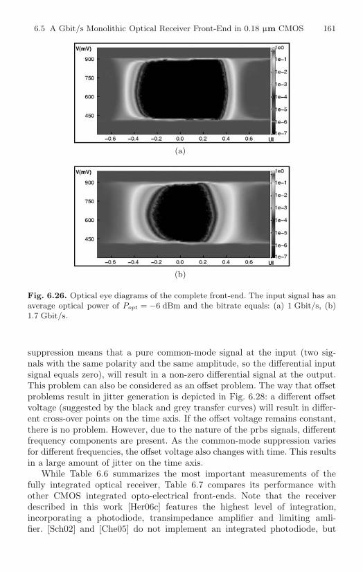
6.5 A Gbit/s Monolithic Optical Receiver Front-End in 0.18 µm CMOS 161
(a)
(b)
Fig. 6.26. Optical eye diagrams of the complete front-end. The input signal has anaverage optical power of Popt = −6 dBm and the bitrate equals: (a) 1 Gbit/s, (b)1.7 Gbit/s.
suppression means that a pure common-mode signal at the input (two sig-nals with the same polarity and the same amplitude, so the differential inputsignal equals zero), will result in a non-zero differential signal at the output.This problem can also be considered as an offset problem. The way that offsetproblems result in jitter generation is depicted in Fig. 6.28: a different offsetvoltage (suggested by the black and grey transfer curves) will result in differ-ent cross-over points on the time axis. If the offset voltage remains constant,there is no problem. However, due to the nature of the prbs signals, differentfrequency components are present. As the common-mode suppression variesfor different frequencies, the offset voltage also changes with time. This resultsin a large amount of jitter on the time axis.
While Table 6.6 summarizes the most important measurements of thefully integrated optical receiver, Table 6.7 compares its performance withother CMOS integrated opto-electrical front-ends. Note that the receiverdescribed in this work [Her06c] features the highest level of integration,incorporating a photodiode, transimpedance amplifier and limiting amli-fier. [Sch02] and [Che05] do not implement an integrated photodiode, but

162 6 CMOS Realizations
(a)
(b)
Fig. 6.27. Electrical eye diagrams of the complete front-end. The input signal hasan equivalent current amplitude of Ieq = 8 µApp and the bitrate equals: (a) 1 Gbit/s,(b) 5 Gbit/s.
perform measurements with commercial photodiodes with a responsivity of0.75 A/W-0.85 A/W. The differential PD of [Her06c] has a responsivity ofonly 0.03 A/W, hence the lower receiver sensitivity. The work presentedin [Roo00] and [Roo01] uses SML-detectors, essentially the same topologyas the differential diode. Their responsivity is larger because older technolo-gies with wider space charge regions are used. [Rad05] includes an integratedphotodiode and outperforms [Her06c] both in speed and in responsivity. Thelatter results from the use of a classical n-well diode with a higher intrinsicresponsivity than the differential photodiode. To increase the n-well diodespeed performance, equalizing techniques have been used. Furthermore, jit-ter problems are much less an issue in this approach due to the nature ofthe signals stemming from the single n-well diode. Combining a differentialphotodiode with equalizing techniques as presented in [Her06c] should resultin a better speed performance. It is strongly believed that, by improving thecommon-mode suppression of the TIA and thus the jitter performance, achiev-ing bitrates of 5 Gbit/s is feasible using an equalized differential photodiodein a 0.18 µm CMOS technology.

6.5 A Gbit/s Monolithic Optical Receiver Front-End in 0.18 µm CMOS 163
t
diff. output
jitter!
diff. input
diff. output
diff. input
t
Fig. 6.28. Generation of jitter due to offset problems.
Table 6.6. Performance summary of the Gbit/s 0.18 µm optical receiver.
Technology 0.18 µm CMOS
Vdd 1.8 V
Optical wavelength 850 nm
photodiode DC responsivity 0.03 A/W
Optical receiver
Bitrate 1.7 Gbit/s
BER@Popt=−6 dBm 10−12
rms jitter 35 ps
Power dissipation 250 mA
Limiting amplifier with output buffer
Bitrate 6 Gbit/s
BER@8 mVpp 10−12
rms jitter 8 ps
Dynamic range 37.5 dB
Power dissipation 210 mA (LA: 40 mA)

164 6 CMOS Realizations
Table 6.7. Comparison of the described optical receiver front-end with other CMOSopto-electrical receivers.
Ref. Technology Bitrate SensitivityIntegration level
PD TIA PA
[Roo00] 0.6 µm 250 Mbit/s −18 dBm x x -
[Roo01] 0.25 µm 700 Mbit/s −18 dBm x x -
[Sch02] 0.35 µm 1.25 Gbit/s −22.5 dBm - x x
[Che05] 0.18 µm 10 Gbit/s −12 dBm - x x
[Rad05] 0.18 µm 3 Gbit/s −19 dBm x x -
[Her06b] 0.18 µm 1.7 Gbit/s −6 dBm x x x
6.6 Conclusions
This chapter has covered the implementation of four standard CMOS chipsthat each contain one or more building blocks of the optical receiver. This way,the theory developed in the previous chapters has been put into practice. Muchattention has been paid to the measurement set-up and the interpretation ofthe measurement results. A systematic approach has been chosen, where thefirst two chip implement test diodes with TIAs, the third chip contains a LA,and the final chip presents a fully integrated optical receiver.
The objective of the first two chips is a demonstration of light detection bystandard CMOS photodiodes. No additional layers or coatings have been usedto enhance the diode speed or responsivity. Furthermore, the performance ofdifferent diode types can be compared, as the circuit has been designed notto be the speed limiting factor. Five test diodes with amplifying circuits havebeen designed in 0.18 µm CMOS, from which the differential n-well diodehas proven to have the best performance. Bitrates up to 500 Mbit/s havebeen demonstrated with a BER in the order of 10−10, where the receiverwith classical n-well diode can achieve a bitrate of 300 Mbit/s for the sameBER. A speed factor improvement of almost two has thus been establishedby applying a clever layout topology for the photodiode. Due to space limi-tations, only three test diodes with amplifiers have been implemented in themore expensive 90 nm technology. The differential diode was left out, and thep+ n-well diode with guard turned out to have the best performance. Bitratesof 500 Mbit/s are achieved with a BER of 10−9. Finally, when the two designsin different CMOS generations are compared, one can conclude that achiev-ing higher bitrates at the receiver front-end becomes more difficult in newerCMOS generations with smaller linewidths. There are two main reasons. First,the intrinsic speed as discussed in Chapter 3 becomes lower due to the smallerspace charge regions. Second, achieving a high extrinsic speed in combinationwith the TIA as discussed in Chapter 4 will become more difficult due to the

Table 6.8. Comparison of the described LAs with other LAs implemented in Bipolar or CMOS technologies.
Ref. Technology Vdd Adiff GBW Bitrate Pdiss SensitivityMax. Offset
signal comp.
[Fau83] 5 µm Bipolar 6 V 60 dB 470 GHz 650 Mbit/s 250 mW 300 µVpp 300 mVpp no
[Rei87] 2 µm Bipolar 5 V 54 dB 1103 GHz 4 Gbit/s 350 mW 2 mVpp 400 mVpp yes
[Poh94] 0.4 µm Bipolar −4 V 45 dB 1600 GHz 10 Gbit/s 400 mW 2.25 mVpp - yes
[Sac00] 0.25 µm CMOS2.5 V
32 dB 119 GHz 2.5 Gbit/s 190 mW 2 mVpp 2 Vpp yes& 3.4 V
[Hol03] 0.18 µm CMOS 1.8 V 43 dB 297 GHz 2 Gbit/s 79 mW - - no
[Gal03] 0.18 µm CMOS 1.8 V 50 dB 2973 GHz 10 Gbit/s 100 mW 4.6 mVpp - yes
[Gal04] 0.18 µm CMOS 2.2 V 15 dB 124 GHz 40 Gbit/s 190 mW - - no
[Cra05] 0.18 µm CMOS 1.8 V 42 dB 393 GHz 3.125 Gbit/s 113 mW 2.5 mVpp 50 mVpp yes
[Her05] 0.18 µm CMOS 1.8 V 27 dB 94 GHz 3.5 Gbit/s 34 mW 10 mVpp - no
[Her06c] 0.18 µm CMOS 1.8 V 38 dB 397 GHz 6 Gbit/s 72 mW 8 mVpp 600 mVpp yes

166 6 CMOS Realizations
higher photodiode junction capacitance at the dominant input node and dueto the limited voltage gain in submicron CMOS technologies.
The next building block implemented in a 0.18 µm CMOS technology hasbeen a limiting amplifier. A Cherry-Hooper topology has been used to broadenthe bandwidth instead of space-consuming passive inductors or noisy active in-ductors. The output buffer necessary to drive the 50 Ω off-chip load comprisestwo fT -doublers. To demonstrate the implemented broadband techniques, eyediagrams with low BER up to 3.5 Gbit/s have been measured. The perfor-mance of this chip competes with present state-of-the-art (Table 6.8).
Finally, all knowledge has been gathered in the design of the fully inte-grated 0.18 µm CMOS optical receiver. It contains a differential photodiode, adifferential TIA, an equalizer to enhance the intrinsic speed of the differentialPD, a high-speed LA with offset-compensation and an output buffer including3 fT -doublers. Applying purely electrical differential signals at the input, thereceiver behaves according to the simulations: bitrates up to 5 Gbit/s havebeen measured with low BER. The stand-alone LA with output buffer canhandle bitrates even up to 6 Gbit/s, and outperforms several recently pub-lished 0.18 µm CMOS LAs (Table 6.8). Further work needs to be done to im-prove the opto-electrical measurements, and the attention should be focusedon the reduction of the jitter due to an insufficient common-mode suppres-sion. However, this work already demonstrates that receiving 850 nm prbslight signals with bitrates higher than 1 Gbit/s is feasible in a mainstreamCMOS technology.

7
Conclusions
After the free fall of the telecommunication industry in the beginning of thiscentury, a gradual recovery started in 2004. At the end of 2006, this positiveevolution continues and people start to dream again. Numerous new opto-electronic applications are emerging, while low cost remains a prime concern.The simple law of economics dictates that the existing III-V compound semi-conductor opto-electronics industry will be affected by optical devices made ofsilicon. Nowadays, silicon devices can achieve almost all of the necessary func-tions for integrated optical devices, like detectors, modulators and switches.Only an electrically powered silicon light source, preferably a laser, is lacking,although successful research is going on also in this field, for instance by In-tel [CP06, Pan05] and by STMicroelectronics [Cof05]. If a commercial siliconlaser finally would be available, the sky is the limit and silicon photonics willbecome reality. It will allow manufacturers to build optical components usingthe same semiconductor equipment and methods they use now for ordinaryintegrated circuits, thereby dramatically lowering the cost of photonics.
The presented work fits in this research on silicon opto-electronics. Tofurther lower the cost, the cheapest technology has been selected: standardCMOS, without any optical tricks or flavors. Of course this mainstream CMOStechnology has an inherent lower performance than dedicated (Bi)CMOS orcompound semiconductor technologies. The goal of this work is to demonstratethe feasibility of light detection in the same CMOS technology that is usedto manufacture standard digital circuits. Furthermore, it is shown in theoryand practice that the inherent low speed performance of CMOS diodes canbe enhanced both on the detector level and on the circuit level. Besides thedesign of the photodiode, the focus lies on the design of the transimpedanceamplifier and the post-amplifier. The main contributions and achievementsare:
• The fundamental laws of semiconductor physics have been reviewed to gainin-depth understanding of the opto-electrical mechanisms in silicon detec-tors. These insights have lead to the development of a one-dimensional
167

168 7 Conclusions
analytical model of the photodiode junction. A complementary numericaltwo-dimensional model has been developed taking into account more sideeffects like retrograde doping profiles and side-wall junctions. These effectsare important for more complicated diode topologies and will also becomemore and more pronounced for the emerging nm-scale technologies. Basedon this two-dimensional model, the theoretical performances of differentkinds of diode topologies have been compared. As the market today ischaracterized by two important phenomena: Moore’s law on the electricalside and the development of new light sources on the optical side, thesetrends have been evaluated using the two-dimensional model.
• An in-depth high-level analysis of the shunt-shunt feedback transimpedanceamplifier has been presented. Analytical equations have been derived forthe transimpedance gain, bandwidth, transimpedance-bandwidth product,loop gain, gain margin and noise. The core amplifier has been modeled as ablack box characterized by DC voltage gain A0, input capacitance Cin andoutput impedances Cout and Rout. The applied assumptions and approx-imations have been pointed out explicitly, as a good designer should beaware that design equations are only valid in a limited design space. How-ever, the trends predicted by these equations form a solid base for a sounddesign. In a next phase, the amplifier’s black box has been opened, anda literature overview of possible implementations has been given. Finally,a detailed study at the transistor level of three different common-sourceTIAs has been presented. Confronting simulation results with design equa-tions has revealed that the basic design assumptions are not always validwhen pushing the performance to its limits. Also a more accurate noisemodel for the photodiode has been elaborated, that takes into account theparasitic series resistance.
• The design of a broadband limiting amplifier, consisting of several cascadedgain stages, has been presented. After a (historical) literature study, aCherry-Hooper topology has been preferred over inductive peaking stages.Analytical design equations have been derived for this broadband stagewhich again form a solid base for a good design. Also for this building blockthe assumptions and approximations made to arrive at the equations havebeen highlighted, so the designer can use them consciously. In addition tothe Cherry-Hooper stage, a capacitive source degenerated stage has beenanalyzed. Finally the technique of offset compensation, indispensable inhigh-performance LAs, has been disclosed. The theory has been completedwith two case studies that clearly illustrate all design choices encounteredduring the design of an analog high-performance circuit.
• An important achievement reached in this work is the systematic anal-ysis, design and implementation of different CMOS photodiode topolo-gies. The photodiodes have been realized together with TIAs and outputbuffers in mainstream CMOS technologies and these opto-electronic cir-cuits have been tested in a real-life measurement set-up. Optical signalsfrom a commercial 850 nm transmitter were applied at the input. The

7 Conclusions 169
conclusion is that a differential photodiode is the best topology choicewhen high bitrates are pursued, at the expense of a lower responsivity. Acomparison of the 0.18 µm PDs with the 90 nm PDs, reveals that technol-ogy downscaling is not beneficial for the overall photodiode performance.Also for the TIA, newer technologies with higher fT ’s are not necessar-ily better, as it becomes more difficult to achieve a high voltage gain insub-micron technologies. This high voltage gain is needed to maximize thetransimpedance-bandwidth product. This should however not impede theCMOS integration of opto-electrical front-ends in future technologies: ana-log design engineers will always be inventive enough to find new solutionsfor new problems.
• To demonstrate the broadband amplifying prospects of CMOS Cherry-Hooper amplifiers, a first LA is designed, manufactured in 0.18 µm CMOSand measured. The experience gained in this design cycle has lead to thedesign and measurements of a second LA incorporating offset compensa-tion. The performance achieved by this circuit outperforms present state-of-the-art. Table 6.8 compares the described LAs with the LAs studied inSection 5.3. Looking at the CMOS implementations, only [Gal03] (whichintegrates passive inductors) has a higher gain-bandwidth than [Her06c].The broadband techniques applied in [Gal03] are undoubtedly very effec-tive to achieve circuits with high gain-bandwidth. However, power dis-sipation of the core amplifier (excluding output buffers) is higher thanin [Her06c].
• The final achievement has also been the largest challenge for the presentedresearch: the realization of a monolithic optical receiver front-end, consist-ing of a PD, TIA and LA. To realize this goal, a very systematic approachhas been chosen, where first the three building blocks have been studiedseparately, but at the same time their mutual impact never has been ne-glected. To enhance the speed performance of the differential photodiodeeven further, an analog equalizer compensates for its frequency roll-off. Ta-ble 6.7 compares the presented work with other state-of-the-art integratedopto-electrical receivers and shows that it features the highest level of in-tegration, while its performance is comparable to other designs. The inputsignals for the photodiode are provided by a commercial available 850 nmoptical transmitter. Finally note that, to the author’s knowledge, the chippresented in [Her06c] is the first monolithic CMOS opto-electrical receiverintegrating photodiode, transimpedance amplifier and limiting amplifier,that achieves bitrates higher than 1 Gbit/s.

References
Agr97. G. P. Agrawal, Fiber-Optic Communication Systems, John Wiley & Sons,second edition, 1997.
Baz91. M. Bazes, “Two Novel Fully Complementary Self-Biased CMOS Differ-ential Amplifiers”, IEEE Journal of Solid-State Circuits, vol. 26, no. 2,pp. 165–168, Feb. 1991.
Cha91. Z. Y. Chang and W. M. C. Sansen, Low-Noise Wide-band Amplifiers inBipolar and CMOS Technologies, Kluwer Academic Publishers, 1991.
Che63. E. M. Cherry and D. E. Hooper, “The Design of Wide-Band Transis-tor Feedback Amplifiers”, Proceedings IEE, vol. 110, no. 2, pp. 375–389,Feb. 1963.
Che05. W.-Z. Chen, Y.-L. Cheng, and D.-S. Lin, “A 1.8-V 10-Gb/s Fully IntegratedCMOS Optical Receiver Analog Front-end”, IEEE Journal of Solid-StateCircuits, vol. 40, no. 6, pp. 1388–1396, June 2005.
Cof05. S. Coffa, “Light From Silicon”, IEEE Spectrum, pp. 36–41, Oct. 2005.Cou97. L. W. Couch, Digital and Analog Communication Systems, Prentice-Hall,
1997.CP06. Y. Carts-Powell, “Innovative Techniques Light Up Silicon Lasers”, Fi-
breSystems Europe/LIGHTWAVE Europe, pp. 33–34, Sept. 2006.Cra05. E. Crain and M. Perrott, “A 3.125 Gb/s Limit Amplifier with 42 dB Gain
and 1 µs Offset Compensation in 0.18-µm CMOS”, in IEEE InternationalSolid-State Circuits Conference, Digest of Technical Papers, pp. 232–233,San Francisco, USA, Feb. 2005.
Csu02. S. M. Csutak, J. B. Schaub, W. E. Wu, and J. C. Campbell, “High-SpeedMonolithically Integrated Silicon Optical Receiver Fabricated in 130-nmCMOS Technology”, IEEE Photonics Technology Letters, vol. 14, no. 4,pp. 516–518, Apr. 2002.
Dor98. R. C. Dorf and R. H. Bishop, Modern Control Systems, Addison-Wesley,1998.
Fau83. D. W. Faulkner, “A Wide-Band Limiting Amplifier for Optical Fiber Re-peaters”, IEEE Journal of Solid-State Circuits, vol. 18, no. 3, pp. 333–340,1983.
Fre. http://www.freescale.com, Freescale Semiconductor–Technologies–Research and Development–Semiconductor R&D Laboratories–Silicon onInsulator.
171

172 References
Fre04. T. Freeman, “Plastic Optical Fibre Tackles Automotive Requirements”,FibreSystems Europe/LIGHTWAVE Europe, pp. 14–16, May 2004.
Gal03. S. Galal and B. Razavi, “10-Gb/s Limiting Amplifier and Laser/ModulatorDriver in 0.18-µm CMOS Technology”, IEEE Journal of Solid-State Cir-cuits, vol. 38, no. 12, pp. 2138–2146, Dec. 2003.
Gal04. S. Galal and B. Razavi, “40-Gb/s Amplifier and ESD Protection Circuitin 0.18-µm CMOS Technology ”, IEEE Journal of Solid-State Circuits,vol. 39, no. 12, pp. 2389–2396, Dec. 2004.
Gen01. J. Genoe, D. Coppee, J. H. Stiens, R. A. Vounckx, and M. Kuijk,“Calculation of the Current Response of the Spatially Modulated LightCMOS Detector”, IEEE Transactions on Electron Devices, vol. 48, no. 9,pp. 1892–1902, Sept. 2001.
Gra02. O. Graydon, “The Terabit Challenge”, Optics & Laser Europe, pp. 31–32,June 2002.
Gra04. O. Graydon, “Photonics Unlocks Chip Bandwidth Bottleneck”, Optics &Laser Europe, pp. 25–27, Oct. 2004.
Her03. C. Hermans, P. Leroux, and M. Steyaert, “Gigabit Photodiodes in Stan-dard Digital nanometer CMOS Technologies”, in Proceedings of the IEEEEuropean Solid-State Device Research Conference, pp. 51–54, Estoril, Por-tugal, Sept. 2003.
Her04a. C. Hermans, P. Leroux, and M. Steyaert, “A High-Speed Optical Front-Endwith Integrated Photodiode in 90 nm CMOS”, in International Symposiumon Signals, Systems and Electronics, Linz, Austria, Aug. 2004.
Her04b. C. Hermans, P. Leroux, and M. Steyaert, “Design of Integrated CMOSPhotodiodes with Low-Noise Amplifiers”, in Tutorial: Integrated OpticalInterface Circuits, ESSCIRC, Leuven, Belgium, Sept. 2004.
Her04c. C. Hermans, P. Leroux, and M. Steyaert, “Two High-Speed OpticalFront-ends with Integrated Photodiodes in Standard 0.18 µm CMOS”,in Proceedings of the IEEE European Solid-State Circuits Conference,pp. 275–278, Leuven, Belgium, Sept. 2004.
Her05. C. Hermans and M. Steyaert, “A 3.5 Gbit/s Post-Amplifier in 0.18 µmCMOS”, in Proceedings of the IEEE European Solid-State Circuits Con-ference, pp. 431–434, Grenoble, France, Sept. 2005.
Her06a. C. Hermans and M. S. J. Steyaert, “A High-Speed 850 nm Optical Re-ceiver Front-end in 0.18 µm CMOS”, IEEE Journal of Solid-State Circuits,vol. 41, no. 7, pp. 1606–1614, July 2006.
Her06b. C. Hermans, F. Tavernier, and M. Steyaert, “A Gigabit Optical Receiverwith Monolithically Integrated Photodiode in 0.18 µm CMOS”, in Proceed-ings of the IEEE European Solid-State Circuits Conference, pp. 476–479,Montreux, Switzerland, Sept. 2006.
Her06c. C. Hermans, F. Tavernier, and M. S. J. Steyaert, “6 Gbit/s LimitingAmplifier with High Dynamic Range in 0.18 µm CMOS”, IEE ElectronicsLetters, vol. 42, no. 18, pp. 1030–1031, Aug. 2006.
Hol03. C. D. Holdenried, M. W. Lynch, and James W. Haslett, “Modified CMOSCherry-Hooper Amplifiers with Source Follower Feedback in 0.35 µm Tech-nology”, in Proceedings of the IEEE European Solid-State Circuits Confer-ence, pp. 553–556, Estoril, Portugal, Sept. 2003.
Ing94. M. Ingels, G. Van de Plas, J. Crols, and M. Steyaert, “A CMOS 18 THzΩ240 Mb/s Transimpedance Amplifier and 155 Mb/s LED-Driver for Low

References 173
Cost Optical Fiber Links”, IEEE Journal of Solid-State Circuits, vol. 29,no. 12, pp. 1552–1559, Dec. 1994.
Ing99. M. Ingels and M. Steyaert, “A 1 Gb/s 0.7 µm CMOS Optical Receiver withFull Rail-to-Rail Output Swing”, IEEE Journal of Solid-State Circuits,vol. 34, no. 7, pp. 971–977, July 1999.
Ing04. M. Ingels and M. Steyaert, Integrated CMOS Circuits for Optical Commu-nications, Springer, 2004.
Jut05. M. Jutzi, M. Grozing, E. Gaugler, W. Mazioschek, and M. Berroth, “2-Gb/s CMOS Optical Integrated Receiver with a Spatially ModulatedPhotodetector”, IEEE Photonics Technology Letters, vol. 17, no. 6,pp. 1268–1270, June 2005.
Kao66. K. C. Kao and G. A. Hockham, “Dielectric fibre surface waveguides foroptical frequencies”, Proceedings IEE, 1966.
Kie03. K. Kieschnick and H. Zimmerman, “High-Sensitivity BiCMOS OEIC forOptical Storage Systems”, IEEE Journal of Solid-State Circuits, vol. 38,no. 4, pp. 579–584, Apr. 2003.
Ler04. P. Leroux, Low-noise Amplification in CMOS High-Frequency Receivers,PhD thesis, K.U.Leuven, Belgium, June 2004.
Lia06. C.-F. Liao and S.-I. Liu, “A 10 Gb/s CMOS AGC Amplifier with 35 dBDynamic Range for 10 Gb Ethernet”, in IEEE International Solid-StateCircuits Conference, Digest of Technical Papers, pp. 516–517, San Fran-cisco, USA, Feb. 2006.
Max05. A. Maxim, “A 12.5 GHz SiGe BICMOS Limiting Amplifier Using a DualOffset Cancellation Loop”, in Proceedings of the IEEE European Solid-State Circuits Conference, pp. 97–100, Grenoble, France, Sept. 2005.
Men. Mentor Graphics Corporation, Eldo Device Equations Manual, v6.5 2,2005.2.
Mil79. S. E. Miller and A. G. Chynoweth, Optical Fiber Telecommunications,Academic Press, 1979.
MIT05. MIT Microphotonics Center Industry Consortium, Microphotonics: Hard-ware for the Information Age, 2005, Communications technology roadmap.
Mol94. M. Moller, H.-M. Rein, and H. Wernz, “13 Gb/s Si-Bipolar AGC AmplifierIC with High Gain and Wide Dynamic Range for Optical-Fiber Receivers”,IEEE Journal of Solid-State Circuits, vol. 29, no. 7, pp. 815–822, July 1994.
Moo65. G. E. Moore, “Cramming More Components onto Integrated Circuits”,Electronics, vol. 38, no. 8, April 1965.
Ove98. R. Van Overstraeten and P. Heremans, Semiconductor Devices, Acco,1998.
Pal01. P. Palojarvi, T. Ruotsalainen, and J. Kostamovaara, “Pn Photodi-odes for Pulsed Laser Rangefinding Applications Realized in StandardCMOS/BiCMOS Processes”, Analog Integrated Circuits and Signal Pro-cessing, vol. 27, pp. 239–248, 2001.
Pan05. M. Paniccia and S. Koehl, “The Silicon Solution”, IEEE Spectrum,pp. 30–35, Oct. 2005.
Par97. S. M. Park and C. Toumazou, “Giga-Hertz Low Noise CMOS Tran-simpedance Amplifier”, in Proceedings IEEE International Symposium onCircuits and Systems, volume 1, pp. 209–212, 1997.
Par00. S. M. Park and C. Toumazou, “A Packaged Low-Noise High-Speed Reg-ulated Cascode Transimpedance Amplifier using 0.6 µm N-well CMOS

174 References
Technology”, in Proceedings of the IEEE European Solid-State CircuitsConference, pp. 432–435, Sept. 2000.
Par04. S. M. Park and H.-J. Yoo, “1.25-Gb/s Regulated Cascode CMOS Tran-simpedance Amplifier for Gigabit Ethernet Applications”, IEEE Journalof Solid-State Circuits, vol. 39, no. 1, pp. 112–121, Jan. 2004.
Pie04. T. Piessens and M. Steyaert, Design and Analysis of High Efficiency LineDrivers for xDSL, Springer, 2004.
Poh94. W. Pohlmann, “A Silicon-Bipolar Amplifier for 10 Gbit/s with 45 dBGain”, IEEE Journal of Solid-State Circuits, vol. 29, no. 5, pp. 551–556,May 1994.
Poh00. K. C. Pohlmann, Principles of Digital Audio, McGraw-Hill, fourth edition,2000.
Rad03. S. Radovanovic, A. J. Annema, and B. Nauta, “Physical and ElectricalBandwidths of Integrated Photodiodes in Standard CMOS Technology”,in IEEE International Conference on Electron Devices and Solid-State Cir-cuits, pp. 95–98, Dec. 2003.
Rad04. S. Radovanovic, A. J. Annema, and B. Nauta, “3 Gb/s MonolithicallyIntegrated Photodiode and Pre-Amplifier in Standard 0.18 µm CMOS”,in IEEE International Solid-State Circuits Conference, Digest of TechnicalPapers, pp. 472–473, San Francisco, USA, Feb. 2004.
Rad05. S. Radovanovic, A. J. Annema, and B. Nauta, “A 3-Gb/s Optical Detectorin Standard CMOS for 850-nm Optical Communication”, IEEE Journalof Solid-State Circuits, vol. 8, no. 40, pp. 1706–1717, Aug. 2005.
Raz02. Behzad Razavi, “Prospects of CMOS Technology for High-Speed OpticalCommunications”, IEEE Journal of Solid-State Circuits, vol. 37, no. 9,pp. 1135–1145, Sept. 2002.
Raz03. B. Razavi, Design of Integrated Circuits for Optical Communications,McGraw-Hill, 2003.
Rei87. R. Reimann and H.-M. Rein, “Bipolar High-Gain Limiting Amplifier ICfor Optical-Fiber Receivers Operating up to 4 Gbit/s”, IEEE Journal ofSolid-State Circuits, vol. 22, no. 4, pp. 504–511, Aug. 1987.
Rei89. R. Reimann and H.-M. Rein, “A Single-Chip Bipolar AGC Ampli-fier with Large Dynamic Range for Optical-Fiber Receivers Operatingup to 3 Gbit/s”, IEEE Journal of Solid-State Circuits, vol. 24, no. 6,pp. 1744–1748, Dec. 1989.
Roo00. C. Rooman, D. Coppee, and M. Kuijk, “Asynchronous 250-Mb/s OpticalReceivers with Integrated Detector in Standard CMOS Technology for Op-tocoupler Applications”, IEEE Journal of Solid-State Circuits, vol. 35, no.7, pp. 953–958, July 2000.
Roo01. C. Rooman, M. Kuijk, R. Windisch, R. Vounckx, G. Borghs, A. Plichta,M. Brinkmann, K. Gerstner, R. Strack, P. Van Daele, W. Woittiez,R. Baets, and P. Heremans, “Inter-chip Optical Interconnects usingImaging Fiber Bundles and Integrated CMOS”, in Proc. 27th Euro-pean Conference on Optical Communication, pp. 296–297, Amsterdam, theNetherlands, Sept. 2001.
Sac00. E. Sackinger and W. C. Fischer, “A 3-GHz 32-dB CMOS Limiting Ampli-fier for SONET OC-48 Receivers”, IEEE Journal of Solid-State Circuits,vol. 35, no. 12, pp. 1884–1888, Dec. 2000.
Sac05. E. Sackinger, Broadband Circuits for Optical Fiber Communication, JohnWiley & Sons, 2005.

References 175
San06. W. M. C. Sansen, Analog Design Essentials, Springer, 2006.Sav02. N. Savage, “Linking with Light”, IEEE Spectrum, pp. 32–36, Aug. 2002.Sch02. K. Schrodinger, J. Stimma, and M. Mauthe, “A Fully Integrated CMOS
Receiver Front-End for Optic Gigabit Ethernet”, IEEE Journal of Solid-State Circuits, vol. 37, no. 7, pp. 874–880, July 2002.
Sei04a. C. Seidl, J. Knorr, and H. Zimmermann, “Compensated Feedback Networkfor Highly Sensitive Optical Receivers”, in International Symposium onSignals, Systems and Electronics, Linz, Austria, Aug. 2004.
Sei04b. C. Seidl, J. Knorr, and H. Zimmermann, “Single-Stage 378 MHz 178 kΩTransimpedance Amplifier with Capacitive-Coupled Voltage Dividers”, inIEEE International Solid-State Circuits Conference, Digest of TechnicalPapers, pp. 470–471, San Francisco, USA, Feb. 2004.
Sei05. C. Seidl, H. Schatzmayr, J. Sturm, S. Groiss, M. Leifhelm, D. Spitzer,H. Schaunig, and H. Zimmermann, “A Programmable OEIC for LaserApplications in the Range from 405 nm to 780 nm”, in Proceedings of theIEEE European Solid-State Circuits Conference, pp. 439–442, Grenoble,France, Sept. 2005.
Stu04. J. Sturm, M. Leifhelm, H. Schatzmayr, S. Groiss, and H. Zimmermann,“Optical Receiver IC for CD/DVD/Blue-Laser Application”, in Proceed-ings of the IEEE European Solid-State Circuits Conference, pp. 267–270,Leuven, Belgium, Sept. 2004.
Stu05. J. Sturm, M. Leifhelm, H. Schatzmayr, S. Groiss, and H. Zimmermann,“Optical Receiver IC for CD/DVD/Blue-Laser Application”, IEEE Journalof Solid-State Circuits, vol. 40, no. 7, pp. 1406–1413, July 2005.
Swo03. R. Swoboda and H. Zimmermann, “A Low-Noise 1.8 Gbps Bipolar OEIC”,in Proceedings of the IEEE European Solid-State Circuits Conference,pp. 314–344, Estoril, Portugal, Sept. 2003.
Swo04. R. Swoboda, J. Knorr, and H. Zimmermann, “A 2.4 GHz-Bandwidth OEICwith Voltage-Up-Converter”, in Proceedings of the IEEE European Solid-State Circuits Conference, pp. 223–226, Leuven, Belgium, Sept. 2004.
Swo05. R. Swoboda, J. Knorr, and H. Zimmermann, “A 5-Gb/s OEIC withVoltage-Up-Converter”, IEEE Journal of Solid-State Circuits, vol. 40,no. 7, pp. 1521–1526, July 2005.
Swo06. R. Swoboda and H. Zimmermann, “11 Gb/s Monolithically IntegratedSilicon Optical Receiver for 850 nm Wavelength”, in IEEE InternationalSolid-State Circuits Conference, Digest of Technical Papers, pp. 240–241,San Francisco, USA, Feb. 2006.
Syn. Synopsis, Medici User Manual, Version 2002.4, Feb. 2003.Tav05. F. Tavernier and M. Steyaert, “Ontwerp van een 2.8 GHz x 3.6 kΩ TIA
en equaliser voor geıntegreerde optische ontvangers”, Master’s thesis,K.U.Leuven, Belgium, 2004-2005.
Tav06. F. Tavernier, C. Hermans, and M. Steyaert, “Optimised Equaliser forDifferential CMOS Photodiodes”, IEE Electronics Letters, vol. 42, no. 17,pp. 1002–1003, Aug. 2006.
Tsa04. C.-M. Tsai, “A 20 mW 85 dBΩ 1.25 Gb/s CMOS Transimpedance Am-plifier with Photodiode Capacitance Cancellation”, in Proceedings of theIEEE Symposium on VLSI Circuits, pp. 408–409, June 2004.
Tsa05a. C.-M. Tsai, “20 mW 1.25 Gb/s CMOS Transimpedance Amplifier with30 dB Dynamic Range”, IEE Electronics Letters, vol. 41, no. 3,pp. 109–110, Feb. 2005.

176 References
Tsa05b. C.-M. Tsai and L.-R. Huang, “A 21 mW 2.5 Gb/s 15 kΩ Self-CompensatedDifferential Transimpedance Amplifier”, in IEEE International Solid-State Circuits Conference, Digest of Technical Papers, pp. 234–235,San Francisco, USA, Feb. 2005.
Tsa06. C.-M. Tsai and L.-R. Huang, “A 24 mW 1.25 Gb/s 13 kΩ TransimpedanceAmplifier Using Active Compensation”, in IEEE International Solid-State Circuits Conference, Digest of Technical Papers, pp. 894–895,San Francisco, USA, Feb. 2006.
UC 04. UC Berkely, BSIM 4.5.0 Model - User’s Manual, 2004.Woo98. T. K. Woodward and A. V. Krishnamoorthy, “1 Gbit/s CMOS Photore-
ceiver with Integrated Photodetector Operating at 850 nm”, IEE Electron-ics Letters, vol. 34, no. 12, pp. 1252–1253, Dec. 1998.
Wu04. C.-H. Wu, C.-S. Liu, and A.-I Liu, “A 2 GHz CMOS Variable-Gain Ampli-fier with 50 dB Linear-in-Magnitude Controlled Gain Range for 10GBase-LX4 Ethernet”, in IEEE International Solid-State Circuits Conference,Digest of Technical Papers, pp. 484–485, San Francisco, USA, Feb. 2004.
Yan03. B. Yang, J. D. Schaub, S. M. Csutak, D. L. Rogers, and J. C. Campbell,“10-Gb/s All-Silicon Optical Receiver”, IEEE Photonics Technology Let-ters, vol. 15, no. 5, pp. 745–747, May 2003.
Yao04. L. Yao, M. Steyaert, and W. Sansen, “A 1-V 88-dB 20-kHz Sigma-Deltamodulator in 90 nm CMOS”, in IEEE International Solid-State CircuitsConference, Digest of Technical Papers, pp. 80–81, San Francisco, USA,Feb. 2004.
Zim04. H. Zimmermann, Silicon Optoelectronics Integrated Circuits, Springer,2004.

Index
absorption coefficient, 28automatic gain control amplifier,
14, 107average mark density, 18
bandwidth-distance product, 7baseline wander, 25BiCMOS, 32bit error rate, 20, 141, 149, 157bit period, 17bitrate, 17bitrate-distance product, 2block coding, 18Blu-Ray Disc, 6, 16, 52burst mode, 19
CD, 16, 52Cherry-Hooper amplifier, 113, 116classical n-well diode, 47, 53, 57, 82, 93,
135, 139, 143, 146clock and data recovery circuit, 14CMOS, 31, 32, 35common gate TIA, 78common source TIA, 77, 81Communications Technology
Roadmap, 7complementary self-biased differential
amplifier, 136continuity equation, 37, 39continuous mode, 19
damping ratio, 65DC wander, 25demultiplexer, 14
depletion region, 28, 30differential n-well diode, 52, 54, 57, 82,
97, 135, 139, 141, 152diffusion, 28, 37, 39drift, 28, 40DVD, 16, 52
electric field, 28electrical sensitivity, 22equalizer, 36, 154extrinsic bandwidth, 31eye diagram, 20, 138, 144, 149, 157
fT -doubler, 148, 156fiber, 2fiber-to-the-home, 4frequency roll-off, 49, 50, 52, 54, 57
gain-bandwidth product, 114
HD-DVD, 6, 16, 52
inductive peaking, 110input dynamic range, 109input offset voltage, 110input-referred noise, 62, 73intersymbol interference, 23intrinsic 3-dB bandwidth, 48, 50, 51,
54, 57intrinsic bandwidth, 31intrinsic frequency characteristic, 48,
50, 53, 55, 56, 58ISSCC, 80
177

178 Index
jitter, 25, 110, 149, 157, 163junction capacitance, 57
Lambert-Beer’s Law, 28laser, 2, 14laser diode, 14laser driver, 14light flux, 30limiting amplifier, 14, 107, 124, 126, 146line coding, 18local area networks, 4long-haul communication systems, 2
measurement set-up, 134Medici, 46modified Cherry-Hooper amplifier, 117modulator driver, 14Moore’s Law, 6, 56multiplexer, 14
n+ p-substrate diode, 82, 135, 140n-well p-substrate junction, 38natural pulsation, 65noise bandwidth, 63non-return-to-zero, 17
offset, 163offset compensation, 122one-dimensional model, 37optical sensitivity, 23optical telegraph, 1output buffer, 143, 147, 156output noise, 62, 71, 73, 89overload current, 63
p+ n-well diode with guard, 49, 82, 93,135, 139, 143, 146, 147
p+ n-well junction with guard, 44PA bandwidth, 109penetration depth, 30phase margin, 69
photodiode, 13, 17, 29, 87, 88photons, 28photophone, 2PIN diode, 33plastic optical fiber, 5POF, 52post-amplifier, 14, 17, 107pseudorandom bit sequence, 18
Q function, 21Q-factor, 145quantum efficiency, 30quasi-fractal n-well diode, 82, 93, 135,
139, 143, 146
regulated cascode TIA, 78responsivity, 30, 48–51, 53–58retrograde well doping profile, 47run length, 18
scrambling, 18sensitivity, 22series-series feedback, 111, 112shot noise, 71shunt-shunt feedback, 63, 111, 112SML-detector, 36, 51SOI, 34space charge region, 28
technology scaling, 57thermal noise, 70, 71TIA bandwidth, 62, 65, 66transceiver, 15transimpedance amplifier, 14, 17, 61,
82, 93, 97transimpedance gain, 61, 64transimpedance-bandwidth product, 67two-dimensional model, 46
wavelength, 52


