12
MF6900A Fading Simulator Product Brochure

MF6900AFading Simulator
Product Brochure

Key Features• High reproducibility and maintainability due to full digital baseband processing• All-in-one unit supports LTE 4×2 MIMO or LTE 2×2 MIMO↔W-CDMA/HSPA dual environment• Easy fading settings using dedicated interface with MD8430A/MD8480C Signalling Tester• Highly extendible hardware platform
Main Uses• Coding and Decoding Tests (RF/Baseband)• Throughput Tests (Performance Tests)• Intra-RAT/Inter-RAT Handover Tests• LTE Pre-conformance/Conformance Tests• LTE Carrier UE Acceptance Tests• Fault Troubleshooting
Functions
All-in-One Full Digital Fading Simulator Supporting LTE 2×2 MIMO 2-cell and 4×2 MIMOThe introduction of the LTE next-generation communication standard makes MIMO evaluation in a fading environment much more complex. Connecting the MF6900A Fading Simulator to the MD8430A Signalling Tester via dedicated digital interface to simulate a BTS greatly simplifies 3GPP LTE 2×2 MIMO and 4×2 MIMO fading tests.
■ With MD8430A (LTE)• 8 channels max. (MIMO)• 1×1 SISO, 1×2 SIMO, 2×1 MISO, 2×2 MIMO (2 cells max.)• 4×1 MISO, 4×2 MIMO (1 cell max.)• Birth-Death/Moving/CQI/HST (2 cells max.)• Correlation Matrix Setting (MIMO)
■ With MD8480C (W-CDMA/HSPA)• 4 channels max.• 1×1 SISO (4 cells max.)• Birth-Death/Moving/HST (4 cells max.)• Tx/TRx Diversity (2 cells max.)• MBMS
■ Common Functions• Path Parameter Edit (12 paths/channel)• Parameter Saving and Reading• Slow Clock Tests• External Control• Clipping
MF6900AFading Simulator
2 Product Brochure l MF6900A

High Reproducibility and Maintainability due to Full Digital Baseband ProcessingThe MF6900A simulates fading using full digital baseband processing. As a result, high-reproducibility results are obtained using the same settings and complex MIMO power control settings are extremely easy and accurate. Moreover, complete elimination of all analog circuits supports easy maintenance and calibration-free stability.
All-in-One Unit Supports LTE 4×2 MIMO or LTE 2×2 MIMO↔W-CDMA/HSPA Dual EnvironmentOne unit supports LTE 2×2 MIMO 2-cell or 4×2 MIMO tests and combination with the MD8430A Signalling Tester offers a simple test setup for intra-system LTE 2×2 MIMO handover or 4×2 MIMO tests
The MD8480C Signalling Tester for W-CDMA supports all-in-one LTE/W-CDMA inter-system handover tests (with MF6900A-001 option installed).
Easy Fading Setting using Dedicated Interface with MD8430A/MD8480CThe MF6900A Fading Simulator uses a dedicated digital connection with the MD8430A/MD8480C. Elimination of internal RF circuits eliminates power control settings, and the simple display supports intuitive use.
In addition, fading setting is made easy just by calling preset fading profiles from MD8430A and MD8480C test scenarios, allowing chipset and UE protocol developers to run tests transparently without a deep understanding of fading settings.
Moreover, auto-synchronization at MD8430A and MD8480C slow clock operation eliminates repeated fading setting.
Expandable Hardware PlatformThe maximum number of input and output ports can be extended to four each to support 4×2 MIMO, 2×2 MIMO with 2 cells and dual RAT between W-CDMA/HSPA. Moreover, the MF6900A has GCF/PTCRB certification with the ME7873F/ME7873L used commonly as an RF conformance test system, and can be used as a future RF conformance test system.
Example of MF6900A Main Display
Product Brochure l MF6900A 3

Panel Layout
Power SwitchAC power On switches Standby to Power On; LED orange at Standby and green at Power On
Hard Disc Access LampOn at hard disk access
Copy KeySaves screen dump of display to files
Recall KeyRecalls parameter files
Save KeySaves parameter files
Local KeySwitches from remote to local mode using GPIB, USB, and Ethernet and enables panel setting
Remote RampOn at remote control
Preset KeyResets parameters to defaults
Function KeySelects and executes function displayed on right (Menu contents change between screens and levels)
Shift KeyToggles function of blue keys; press until LED is green and press required key.
Main Function KeyFor connecting USB memory or USB keyboard and mouse
Rotary Knob/Cursor Key/Enter Key/Cancel KeySelect and change settings of displayed items
Numerical KeypadSets parameters
USB Connector (Type A)For connecting USB flash memory, USB keyboard or mouse
• Front Panel
4 Product Brochure l MF6900A

Port 1, 2, 3, 4 (LVDS)Input and output IQ signals. Connect with MD8480C BTS board LVDS connector or MD8430A Fading Simulator Interface LVDS connector using attached LVDS cable. Standard configuration connects to two ports. Adding MF6900A-001 option supports maximum of four port connections.
AC InletFor connecting power cord
Monitor OutFor connecting external display
USBFor connecting USB flash memory, USB keyboard or mouse
LANFor connecting external controller (PC) or Ethernet network
USB (Remote)For connecting external controller over USB
GPIBFor connecting external controller over GPIB
AuxFor future function expanded functions
Sampling ClockFor connecting MD8480C Clock Output to input timing Clock; Sampling Clock1 and 2 can be selected for each port.
Sync StartFor connecting Sync Output MD8480C or MD8430A to input Data output trigger. Sync Start1 and 2 can be selected for each port.
Trigger InputFor future function expanded functions
• Rear Panel
Product Brochure l MF6900A 5

Options/SoftwareOptions
MF6900A-001 Additional LVDS InterfaceHardware option to add two rear LVDS interface portsRequired when using 2 cells with MD8430A and 3 or more cells with MD8480C
MF6900A-101 Additional LVDS Interface RetrofitFor MF6900A-001 retrofit at Anritsu plant
Software Options
MX690010A 2×2 MIMOSoftware installed in main frame to use LTE MIMO functions
MX690010A-001 4×2 MIMOSoftware installed option adding 4×2 MIMO capability
MX690011A Propagation for CQI testSoftware installed option adding test conditions specified by 3GPP TS 36.521-1 Chapter 9.3 CQI Reporting under fading conditions and Chapter 9.4 Reporting of Precoding Matrix Indicator (PMI)
MX690020A WCDMA Extended ModelSoftware installed in main frame to use Moving, Birth-Death, Tx/TRx Diversity functions∗: Connection with MD8480C requires MU848072C-40 MF6900 interface or MU848072E BTS Evolution option
MX690030A High Speed TrainSoftware installed option adding High Speed Train (HST) Scenario that is one of the mobility condition specified by 3GPP
Standard configuration MX690010A MX690020A
Max. No. of LTE BS (MD8430A) Max. No. of W-CDMA BS (MD8480C)– MF6900A-001 – MF6900A-001
SISO (Standard) √ – – 1 2 2 4LTE MIMO, MISO, SIMO – √ – 1 2 – –LTE Diversity – √ – 1 2 – –LTE 2×2 MIMO Handover – √∗ – – 2 – –LTE, W-CDMA/HSPA Inter-RAT – √∗ √ – 1 – 2
Birth-Death – – √ 1 2 2 4Moving – – √ 1 2 2 4W-CDMA/HSPA Diversity – – √ – – 1 2W-CDMA MBMS √∗ – – – – – 4
∗: Requires MF6900A-001 Additional LVDS Interface option
Fading Profile
SISOCase1, Case2, Case3, Case4, Case5, Case6, Case8, VA3, VA30, VA120, PA3, PB3[3GPP TS 25.101 V8.9.0 (2009-12), TS 34.121-1 V8.9.0 (2009-12)]EPA, EVA, ETU [3GPP TS 36.101 V8.8.0 (2009-12)]
2×2 MIMO/1×2 SIMO∗1 EPA, EVA, ETU [3GPP TS 36.101 V8.8.0 (2009-12)]4×2 MIMO/4×1 MISO∗2 EPA, EVA, ETU [3GPP TS 36.101 V8.8.0 (2009-12)]1×2 CQI/1×1 CQI∗3 Fading conditions for CQI tests [3GPP TS 36.101 V8.8.0 (2009-12)]2×2 HST/1×2 HST/1×1 HST∗4 HST [3GPP TS 25.101 V8.9.0 (2009-12), TS 34.121-1 V8.9.0 (2009-12)] [3GPP TS 36.101 V8.8.0 (2009-12)]Moving∗5 Moving propagation conditions [3GPP TS 25.101 V8.9.0 (2009-12)]Birth-Death∗5 Birth-Death propagation conditions [3GPP TS 25.101 V8.9.0 (2009-12)]
Tx/TRx Diversity∗5 Case1, Case2, Case3, Case4, Case5, Case6, Case8, VA3, VA30, VA120, PA3, PB3[3GPP TS 25.101 V8.8.0 (2009-12) , TS 34.121-1 V8.9.0 (2009-12)]
∗1: Requires MX690010A 2×2 MIMO option∗2: Requires MX690010A 2×2 MIMO and MX690010A-001 4×2 MIMO option∗3: Requires MX690011A Propagation for CQI test option∗4: Requires MX690030A High Speed Train option∗5: Requires MX690020A WCDMA Extended model option
6 Product Brochure l MF6900A

SpecificationsMF6900A Fading Simulator
Connector
Digital I/F I/F (Rear panel) for exchanging signals between MF6900A and MD8480C or MF6900A and MD8430A with one connector supporting both input and output
No. of I/O Ports 2 ports (Standard), 4 ports (with MF6900A-001 Additional LVDS Interface (Opt-001))
Sampling Clock I/F for adjusting timing between MF6900A and MD8480C with two system settings (Sampling Clock1, Sampling Clock2)
Electrical Characteristics Connector: BNC-J (Rear panel)Input level: LVTTL
Sync Start I/F for synchronizing between MF6900A and MD8480C, or between MF6900A and MD8430A with two settings (Sync Start1, Sync Start2)
Electrical Characteristics Connector: BNC-J (Rear panel)Input level: LVTTL
External Controller Supports control from external controller (except Power Supply)Ethernet(10/100/1000 BASE-T) Connector: RJ-45 (Rear panel)
GPIBSupports IEEE488.2Connector: IEEE bus connector (Rear panel)Interface functions: SH1, AH1, T6, L4, SR1, RL1, PP0, DC1, DT0, C0, E2
USB (B) Supports USB2.0Connector: USB-B (Rear panel)
USBFor connecting external USB devices to save mainframe parametersSupports USB2.0Connector: USB-A (Front panel: 2 ports, Rear panel: 2 ports)
Monitor Out Connector: Mini D-Sub 15 pins, VGA compatible (Rear panel)
Display XGA color LCD (Resolution: 1024 × 768)8.4 inches (213 mm diagonal)
Common Parameter
Defined by Digital I/F
RF Frequency 100 MHz to 6000 MHz, Resolution: 1 Hz (except 1×1 HST/1×2 HST/2×2 HST)89.937737 MHz to 36154.970475 MHz, Resolution: 1 Hz (1×1 HST/1×2 HST/2×2 HST, Display only)
Sampling Frequency10 MHz to 80 MHz, Resolution: 1 Hz (except 1×1 HST/1×2 HST/2×2 HST)19.2 MHz, 30.72 MHz (1×1 HST/1×2 HST/2×2 HST)∗
∗ To assume normal simulator operation, it is necessary to set the input signal sampling frequencyPort Gain –50 to 0 dB, Resolution: 0.1 dB, Setting accuracy: 0.05 dB, each port can be setRelative Channel Gain –50 to 0 dB, Resolution: 0.1 dB, Setting accuracy: 0.05 dB, each channel can be set
Doppler Frequency 0 or 0.1 Hz to 20 kHz, Resolution: 0.01 Hz (except 1×1 HST/1×2 HST/2×2 HST)50 Hz to 3350 Hz, Resolution: 1 Hz (1×1 HST/1×2 HST/2×2 HST)
Moving Speed
0 km/h to νmax km/h, Resolution: 0,01 km/h (except 1×1 HST/1×2 HST/2×2 HST)where νmax found as;
νmax = c fd fc
fc (Hz): Frequency, c: Velocity of light in vacuum (1.07925825 × 10⁹ km/h),fd: Maximum doppler frequency at 20 kHz
100 km/h to 600 km/h, Resolution: 100 km/h (1×1 HST/1×2 HST/2×2 HST)
Channel Configuration (SISO)
Defined by Digital I/FNumber of Port 2 (Standard), 4 (with Opt-001)Number of Channel 2 (Standard), 4 (with Opt-001)Number of Path 12 paths/channel
Relative Path Delay 0 to 600 μs, Resolution: 0.1 ns, Setting accuracy: ±0.1 ns∗ Based on delay 0, when connecting MD8430A or MD8480C
Relative Path Gain –50 to 0 dB, Resolution: 0.1 dB, Setting accuracy: 0.05 dB
Fading Type Constant Phase, Pure Doppler, Rayleigh model, Rice model∗ Pure Doppler and Rice model can only be set for 1 path at 1 channel
Phase Shift Constant Phase0 to 359.9°, Resolution: 0.1°, Setting accuracy: 0.1°
Rice K Factor Rice model+30 to –30 dB, Resolution: 0.1 dB
Angle of Arrival Pure Doppler or Rice model0 to 359.9°, Resolution: 0.1°
Standard Fading ProfileCase1, Case2, Case3, Case4, Case5, Case6, Case8, VA3, VA30, VA120, PA3, PB3
[3GPP TS 25.101 V8.9.0 (2009-12), TS 34.121-1 V8.9.0 (2009-12)], EPA, EVA, ETU [3GPP TS 36.101 V8.8.0 (2009-12)]
Product Brochure l MF6900A 7

Channel Configuration ( 2×2 MIMO/ 2×1 MISO/ 1×2 SIMO)
Enabled with MX690010A and when MD8430A connected, Defined by Digital I/FNumber of Port 2 (Standard), 2+2 (with Opt-001)
Number of Channel 2×2 MIMO: 4 (Standard), 4+4 (with Opt-001)2×1 MISO/1×2 SIMO: 2 (Standard), 2+2 (with Opt-001)
Number of Path 12 paths/channel
Relative Path Delay 0 to 600 μs, Resolution: 0.1 ns, Setting accuracy: ±0.1 ns∗ Based on delay 0, when connecting MD8430A
Relative Path Gain –50 to 0 dB, Resolution: 0.1 dB, Setting accuracy: 0.05 dB
Fading Type Constant Phase, Pure Doppler, Rayleigh model, Rice model∗ Pure Doppler and Rice model can only be set for 1 path at 1 channel
Phase Shift Constant Phase0 to 359.9°, Resolution: 0.1°, Setting accuracy: 0.1°
Rice K Factor Rice model+30 to –30 dB, Resolution: 0.1 dB
Angle of Arrival Pure Doppler or Rice model0 to 359.9°, Resolution: 0.1°
Correlation Matrix
4×4 (2×2 MIMO), 2×2 (1×2 MISO, 2×1 SIMO)A 3GPP TS 36.101 V8.8.0 (2009-12) compliant correlation matrix can be set2×2 High Correlation, 2×2 Medium Correlation, 2×2 Low Correlation
Arbitrary correlation matrix can be set by following correlation coefficient range–1.00000 to 1.00000, Resolution: 0.00001 (Display only)
Standard Fading Profile EPA, EVA, ETU [3GPP TS 36.101 V8.8.0 (2009-12)]Correlation Coefficient –0.99 to 0.99, Resolution: 0.01
Channel Configuration (Moving)
Enabled with MX690020A, Defined by Digital I/FNumber of Port 2 (Standard), 4 (with Opt-001)Number of Channel 2 (Standard), 4 (with Opt-001)Standard Fading Profile Moving Propagation conditions [3GPP TS 25.101 V8.9.0 (2009-12)]Delay Variation 0.5 μs to 10 μs, Resolution: 0.1 μs, Setting accuracy: 2 nsDelay Offset 0 to 50 μs, Resolution: 0.1 μs, Setting accuracy: 0.1 nsAngular Frequency (ω) 0.01 rad/s to 0.4 rad/s, Resolution: 0.01 rad/s, Setting accuracy: 0.0001 rad/s
Variation Period
15.708 s to 628.318 s, Resolution: 0.001 s (Display only)where ω (rad/s) and Ts found as;
ω = 2π T
Relative Path Gain –50 to 0 dB, Resolution: 0.1 dB, Setting accuracy: 0.05 dB
Channel Configuration (Birth-Death)
Enabled with MX690020A, Defined by Digital I/FNumber of Port 2 (Standard), 4 (with Opt-001)Number of Channel 2 (Standard), 4 (with Opt-001)Standard Fading Profile Birth-Death propagation conditions [3GPP TS 25.101 V8.9.0 (2009-12)]Maximum Delay 1 μs to 600 μs, Resolution: 0.1 ns
Delay Resolution0.1 μs to 60 μs, Resolution: 0.1 μs, Setting accuracy: 0.1 ns
where Delay resolution: ∆T (μs) and Maximum delay: Tmax (μs) found as; 10•∆T = Tmax
Dwell Time 0.1 ms to 2000 ms, Resolution: 0.1 ms, Setting accuracy: 0.05 μsRelative Path Gain –50 to 0 dB, Resolution: 0.1 dB, Setting accuracy: 0.05 dB
Channel Configuration ( Tx/Trx diversity)
Enabled with MX690020A and when MD8480C connected, Defined by Digital I/FNumber of Port 2 (Standard), 4 (with Opt-001)
Number of Channel Tx Diversity: 2 (Standard), 2+2 (with Opt-001)Trx Diversity: 4 (Standard), 4+4 (with Opt-001)
Number of Path 12 paths/channel
Relative Path Delay 0 to 600 μs, Resolution: 0.1 ns, Setting accuracy: ±0.1 ns∗ Based on delay 0, when connecting MD8480C
Relative Path Gain –50 to 0 dB, Resolution: 0.1 dB, Setting accuracy: 0.05 dB
Fading Type Constant Phase, Pure Doppler, Rayleigh model, Rice model∗ Pure Doppler and Rice model can only be set for 1 path at 1 channel
Phase Shift Constant Phase0 to 359.9°, Resolution: 0.1°, Setting accuracy: 0.1°
Rice K Factor Rice model+30 to –30 dB, Resolution: 0.1 dB
Angle of Arrival Pure Doppler or Rice model0 to 359.9°, Resolution: 0.1°
Standard Fading Profile Case1, Case2, Case3, Case4, Case5, Case6, Case8, VA3, VA30, VA120, PA3, PB3[3GPP TS 25.101 V8.9.0 (2009-12), TS 34.121-1 V8.9.0 (2009-12)]
8 Product Brochure l MF6900A
Channel Configuration ( 4×2 MIMO/ 4×1 MISO)
Enabled with MF6900A-001, MX690010A, MX690010A-001 and when MD8430A connected, Defined by Digital I/FNumber of Port 4Number of Channel 4×2 MIMO: 8, 4×1 MISO: 4Number of Path 12 paths/channel
Relative Path Delay 0 to 600 μs, Resolution: 0.1 ns, Setting accuracy: ±0.1 ns∗ Based on delay 0, when connecting MD8430A
Relative Path Gain –50 to 0 dB, Resolution: 0.1 dB, Setting accuracy: 0.05 dB
Fading Type Constant Phase, Pure Doppler, Rayleigh model, Rice model∗ Pure Doppler and Rice model can only be set for 1 path at 1 channel
Phase Shift Constant Phase0 to 359.9°, Resolution: 0.1°, Setting accuracy: 0.1°
Rice K Factor Rice model+30 to –30 dB, Resolution: 0.1 dB
Angle of Arrival Pure Doppler or Rice model0 to 359.9°, Resolution: 0.1°
Correlation Coefficient –0.99 to 0.99, Resolution: 0.01
Correlation Matrix
8×8 (4×2 MIMO), 4×4 (4×1 MISO) A 3GPP TS 36.101 V8.8.0 (2009-12) compliant correlation matrix can be set4×2 High Correlation, 4×2 Medium Correlation, 4×2 Low Correlation∗ when using Scaling factor
Arbitrary correlation matrix can be set by following correlation coefficient range–1.00000 to 1.00000, Resolution: 0.00001 (Display only)
Standard Fading Profile EPA, EVA, ETU [3GPP TS 36.101 V8.8.0 (2009-12)]
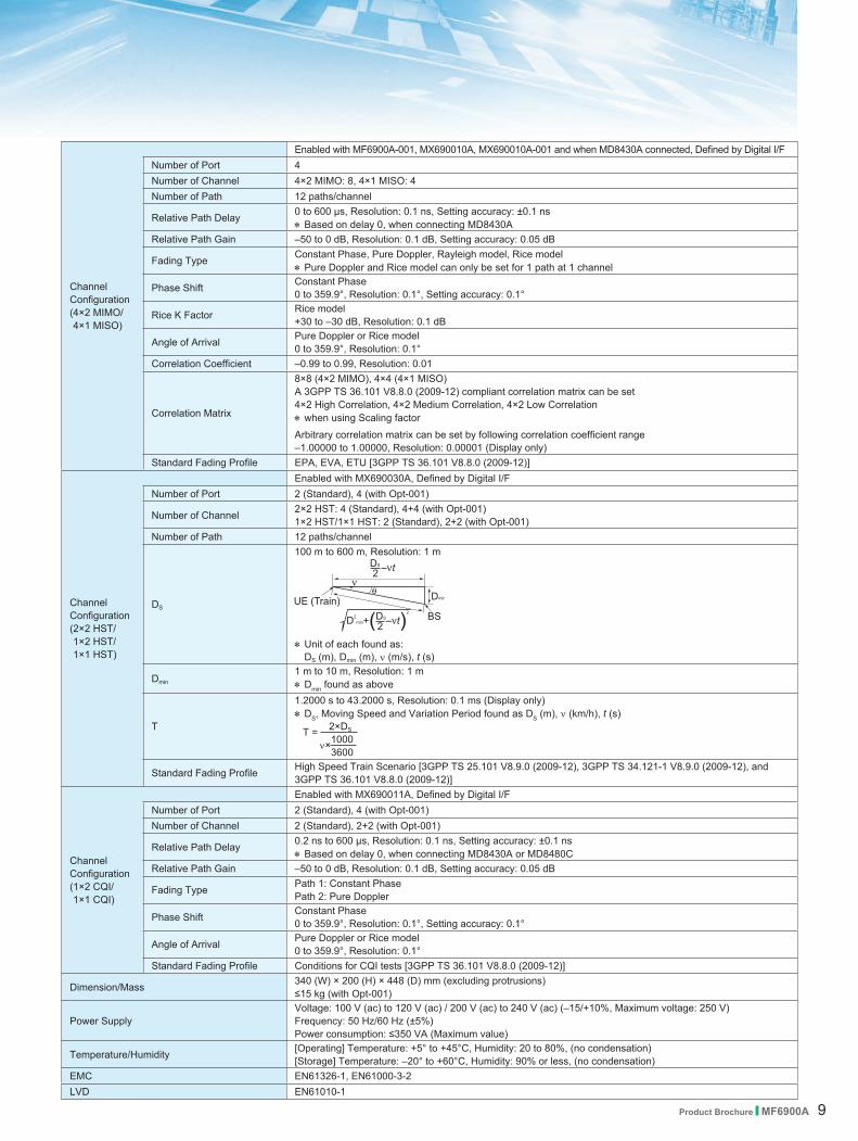
Channel Configuration ( 2×2 HST/ 1×2 HST/ 1×1 HST)
Enabled with MX690030A, Defined by Digital I/FNumber of Port 2 (Standard), 4 (with Opt-001)
Number of Channel 2×2 HST: 4 (Standard), 4+4 (with Opt-001)1×2 HST/1×1 HST: 2 (Standard), 2+2 (with Opt-001)
Number of Path 12 paths/channel
DS
100 m to 600 m, Resolution: 1 m
∗ Unit of each found as: DS (m), Dmin (m), ν (m/s), t (s)
Dmin1 m to 10 m, Resolution: 1 m∗ Dmin found as above
T
1.2000 s to 43.2000 s, Resolution: 0.1 ms (Display only)∗ DS, Moving Speed and Variation Period found as DS (m), ν (km/h), t (s)
T = 2×DS ν×1000 3600
Standard Fading Profile High Speed Train Scenario [3GPP TS 25.101 V8.9.0 (2009-12), 3GPP TS 34.121-1 V8.9.0 (2009-12), and 3GPP TS 36.101 V8.8.0 (2009-12)]
Channel Configuration ( 1×2 CQI/ 1×1 CQI)
Enabled with MX690011A, Defined by Digital I/FNumber of Port 2 (Standard), 4 (with Opt-001) Number of Channel 2 (Standard), 2+2 (with Opt-001)
Relative Path Delay 0.2 ns to 600 μs, Resolution: 0.1 ns, Setting accuracy: ±0.1 ns∗ Based on delay 0, when connecting MD8430A or MD8480C
Relative Path Gain –50 to 0 dB, Resolution: 0.1 dB, Setting accuracy: 0.05 dB
Fading Type Path 1: Constant PhasePath 2: Pure Doppler
Phase Shift Constant Phase0 to 359.9°, Resolution: 0.1°, Setting accuracy: 0.1°
Angle of Arrival Pure Doppler or Rice model0 to 359.9°, Resolution: 0.1°
Standard Fading Profile Conditions for CQI tests [3GPP TS 36.101 V8.8.0 (2009-12)]
Dimension/Mass 340 (W) × 200 (H) × 448 (D) mm (excluding protrusions)≤15 kg (with Opt-001)
Power SupplyVoltage: 100 V (ac) to 120 V (ac) / 200 V (ac) to 240 V (ac) (–15/+10%, Maximum voltage: 250 V)Frequency: 50 Hz/60 Hz (±5%)Power consumption: ≤350 VA (Maximum value)
Temperature/Humidity [Operating] Temperature: +5° to +45°C, Humidity: 20 to 80%, (no condensation)[Storage] Temperature: –20° to +60°C, Humidity: 90% or less, (no condensation)
EMC EN61326-1, EN61000-3-2LVD EN61010-1
Product Brochure l MF6900A 9
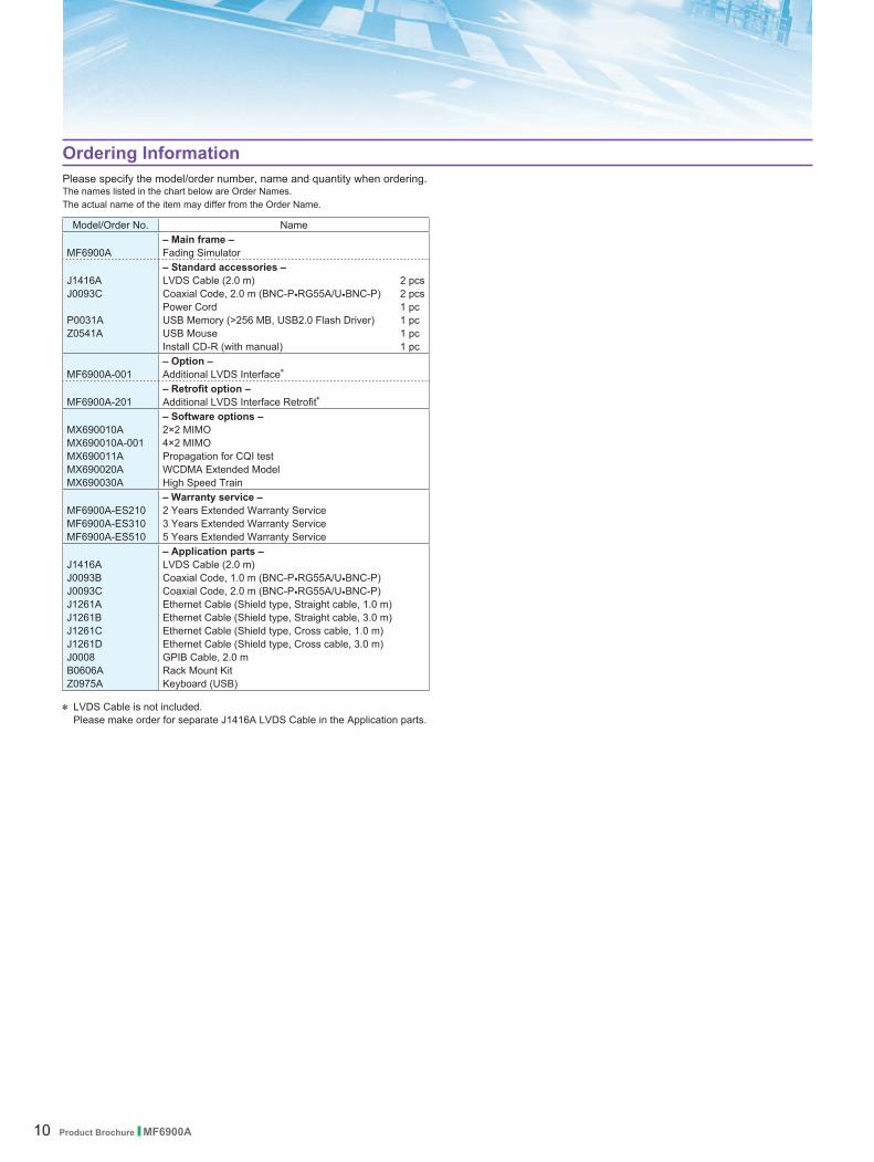
Ordering InformationPlease specify the model/order number, name and quantity when ordering.The names listed in the chart below are Order Names. The actual name of the item may differ from the Order Name.
Model/Order No. Name
MF6900A– Main frame –Fading Simulator
J1416AJ0093C
P0031AZ0541A
– Standard accessories –LVDS Cable (2.0 m) 2 pcsCoaxial Code, 2.0 m (BNC-P•RG55A/U•BNC-P) 2 pcsPower Cord 1 pcUSB Memory (>256 MB, USB2.0 Flash Driver) 1 pcUSB Mouse 1 pcInstall CD-R (with manual) 1 pc
MF6900A-001– Option –Additional LVDS Interface∗
MF6900A-201– Retrofit option –Additional LVDS Interface Retrofit∗
MX690010AMX690010A-001MX690011AMX690020AMX690030A
– Software options –2×2 MIMO4×2 MIMOPropagation for CQI testWCDMA Extended ModelHigh Speed Train
MF6900A-ES210MF6900A-ES310MF6900A-ES510
– Warranty service –2 Years Extended Warranty Service3 Years Extended Warranty Service5 Years Extended Warranty Service
J1416AJ0093BJ0093CJ1261AJ1261BJ1261CJ1261DJ0008B0606AZ0975A
– Application parts –LVDS Cable (2.0 m)Coaxial Code, 1.0 m (BNC-P•RG55A/U•BNC-P)Coaxial Code, 2.0 m (BNC-P•RG55A/U•BNC-P)Ethernet Cable (Shield type, Straight cable, 1.0 m)Ethernet Cable (Shield type, Straight cable, 3.0 m)Ethernet Cable (Shield type, Cross cable, 1.0 m)Ethernet Cable (Shield type, Cross cable, 3.0 m)GPIB Cable, 2.0 mRack Mount KitKeyboard (USB)
∗ LVDS Cable is not included. Please make order for separate J1416A LVDS Cable in the Application parts.
10 Product Brochure l MF6900A

Note:
Product Brochure l MF6900A 11

Anritsu Corporation 5-1-1 Onna, Atsugi-shi, Kanagawa, 243-8555 JapanPhone: +81-46-223-1111Fax: +81-46-296-1238
• U.S.A.Anritsu Company1155 East Collins Blvd., Suite 100, Richardson, TX 75081, U.S.A.Toll Free: 1-800-267-4878Phone: +1-972-644-1777Fax: +1-972-671-1877
• CanadaAnritsu Electronics Ltd.700 Silver Seven Road, Suite 120, Kanata, Ontario K2V 1C3, CanadaPhone: +1-613-591-2003 Fax: +1-613-591-1006
• Brazil Anritsu Eletrônica Ltda.Praça Amadeu Amaral, 27 - 1 Andar01327-010 - Bela Vista - São Paulo - SP - BrasilPhone: +55-11-3283-2511Fax: +55-11-3288-6940
• MexicoAnritsu Company, S.A. de C.V.Av. Ejército Nacional No. 579 Piso 9, Col. Granada11520 México, D.F., MéxicoPhone: +52-55-1101-2370Fax: +52-55-5254-3147
• U.K.Anritsu EMEA Ltd.200 Capability Green, Luton, Bedfordshire, LU1 3LU, U.K.Phone: +44-1582-433200 Fax: +44-1582-731303
• FranceAnritsu S.A.12 avenue du Québec, Bâtiment Iris 1- Silic 612,91140 VILLEBON SUR YVETTE, FrancePhone: +33-1-60-92-15-50Fax: +33-1-64-46-10-65
• GermanyAnritsu GmbHNemetschek Haus, Konrad-Zuse-Platz 1 81829 München, Germany Phone: +49-89-442308-0 Fax: +49-89-442308-55
• ItalyAnritsu S.r.l.Via Elio Vittorini 129, 00144 Roma, ItalyPhone: +39-6-509-9711 Fax: +39-6-502-2425
• SwedenAnritsu ABBorgafjordsgatan 13, 164 40 KISTA, SwedenPhone: +46-8-534-707-00 Fax: +46-8-534-707-30
• FinlandAnritsu ABTeknobulevardi 3-5, FI-01530 VANTAA, FinlandPhone: +358-20-741-8100Fax: +358-20-741-8111
• DenmarkAnritsu A/S (Service Assurance)Anritsu AB (Test & Measurement)Kirkebjerg Allé 90, DK-2605 Brøndby, DenmarkPhone: +45-7211-2200Fax: +45-7211-2210
• RussiaAnritsu EMEA Ltd. Representation Office in RussiaTverskaya str. 16/2, bld. 1, 7th floor.Russia, 125009, MoscowPhone: +7-495-363-1694Fax: +7-495-935-8962
• United Arab EmiratesAnritsu EMEA Ltd.Dubai Liaison OfficeP O Box 500413 - Dubai Internet CityAl Thuraya Building, Tower 1, Suit 701, 7th FloorDubai, United Arab EmiratesPhone: +971-4-3670352Fax: +971-4-3688460
• SingaporeAnritsu Pte. Ltd.60 Alexandra Terrace, #02-08, The Comtech (Lobby A)Singapore 118502Phone: +65-6282-2400Fax: +65-6282-2533
• IndiaAnritsu Pte. Ltd. India Branch Office3rd Floor, Shri Lakshminarayan Niwas, #2726, 80 ft Road, HAL 3rd Stage, Bangalore - 560 075, IndiaPhone: +91-80-4058-1300Fax: +91-80-4058-1301
• P.R. China (Hong Kong)Anritsu Company Ltd.Units 4 & 5, 28th Floor, Greenfield Tower, Concordia Plaza, No. 1 Science Museum Road, Tsim Sha Tsui East, Kowloon, Hong KongPhone: +852-2301-4980Fax: +852-2301-3545
• P.R. China (Beijing)Anritsu Company Ltd.Beijing Representative OfficeRoom 2008, Beijing Fortune Building, No. 5, Dong-San-Huan Bei Road, Chao-Yang District, Beijing 100004, P.R. ChinaPhone: +86-10-6590-9230Fax: +86-10-6590-9235
• KoreaAnritsu Corporation, Ltd.8F Hyunjuk Building, 832-41, Yeoksam Dong, Kangnam-ku, Seoul, 135-080, KoreaPhone: +82-2-553-6603Fax: +82-2-553-6604
• AustraliaAnritsu Pty. Ltd.Unit 21/270 Ferntree Gully Road, Notting Hill, Victoria 3168, AustraliaPhone: +61-3-9558-8177Fax: +61-3-9558-8255
• TaiwanAnritsu Company Inc.7F, No. 316, Sec. 1, Neihu Rd., Taipei 114, TaiwanPhone: +886-2-8751-1816Fax: +886-2-8751-1817
Specifications are subject to change without notice.
Catalog No. MF6900A-E-A-1-(2.00) Printed in Japan 17/NOV/2010 ddcw/CDT
1010
Printed on Recycled Paper
Please Contact:


