October 2010 Doc ID 17784 Rev 1 1/24 AN3255 Application note Building an RFID short-range reader using the STM8S-DISCOVERY Application overview High frequency 13,56 MHz RFID solutions offer ideal close-proximity identification for product authentication, parcel tracking, document management, library and ticketing applications. This application note describes how to build an RFID (radio frequency identification) short- range reader using STMicroelectronics STM8S-DISCOVERY and ISO14443 type-B CR14 contactless coupler. The STM8S-DISCOVERY and the CR14 communicate through an I 2 C bus. The resulting RFID reader can exchange data with ISO 14443-2 type-B proximity PICCs (proximity integrated coupling cards) also called tags. Communications are possible only when the tags are present in the electromagnetic field generated by the reader built-in antenna. Once the STM8S-DISCOVERY is powered up through a USB cable connected to the host PC, an electromagnetic field is generated by the RFID reader. A beep is emitted and the LED LD1 briefly lights up when an ISO 14443-2 type-B proximity tag is detected by the reader and its unique identifier (UID) successfully read. The STM8S-DISCOVERY can be used to evaluate the main features of all STM8S MCUs, even if it is built on an STM8S105C6T6. Reference documents ■ STM8S-DISCOVERY evaluation board user manual (UM0817). ■ Developing and debugging your STM8S-DISCOVERY application code (UM0834). ■ User manual “CR14 and CRX14 reference design PCB Gerber files” (UM0672) and RFID Gerber files. ■ CR14 datasheet: “Low cost ISO14443 type-B contactless coupler chip with anti-collision and CRC management” ■ SRI2K datasheet: “13,56 MHz short-range contactless memory chip with 2048 bit EEPROM and anti-collision functions” ■ Application note “Antenna (and associated components) matching-circuit calculation of the CRX14 coupler” (AN1806) ■ Application note “How to design a 13.56 MHz customized antenna” (AN2866) These documents can be downloaded from http://www.st.com. www.st.com
Transcript
October 2010 Doc ID 17784 Rev 1 1/24
AN3255Application note
Building an RFID short-range readerusing the STM8S-DISCOVERY
Application overviewHigh frequency 13,56 MHz RFID solutions offer ideal close-proximity identification for product authentication, parcel tracking, document management, library and ticketing applications.
This application note describes how to build an RFID (radio frequency identification) short-range reader using STMicroelectronics STM8S-DISCOVERY and ISO14443 type-B CR14 contactless coupler. The STM8S-DISCOVERY and the CR14 communicate through an I2C bus.
The resulting RFID reader can exchange data with ISO 14443-2 type-B proximity PICCs (proximity integrated coupling cards) also called tags. Communications are possible only when the tags are present in the electromagnetic field generated by the reader built-in antenna.
Once the STM8S-DISCOVERY is powered up through a USB cable connected to the host PC, an electromagnetic field is generated by the RFID reader. A beep is emitted and the LED LD1 briefly lights up when an ISO 14443-2 type-B proximity tag is detected by the reader and its unique identifier (UID) successfully read.
The STM8S-DISCOVERY can be used to evaluate the main features of all STM8S MCUs, even if it is built on an STM8S105C6T6.
Reference documents
■ STM8S-DISCOVERY evaluation board user manual (UM0817).
■ Developing and debugging your STM8S-DISCOVERY application code (UM0834).
■ User manual “CR14 and CRX14 reference design PCB Gerber files” (UM0672) and RFID Gerber files.
■ CR14 datasheet: “Low cost ISO14443 type-B contactless coupler chip with anti-collision and CRC management”
■ SRI2K datasheet: “13,56 MHz short-range contactless memory chip with 2048 bit EEPROM and anti-collision functions”
■ Application note “Antenna (and associated components) matching-circuit calculation of the CRX14 coupler” (AN1806)
■ Application note “How to design a 13.56 MHz customized antenna” (AN2866)
These documents can be downloaded from http://www.st.com.
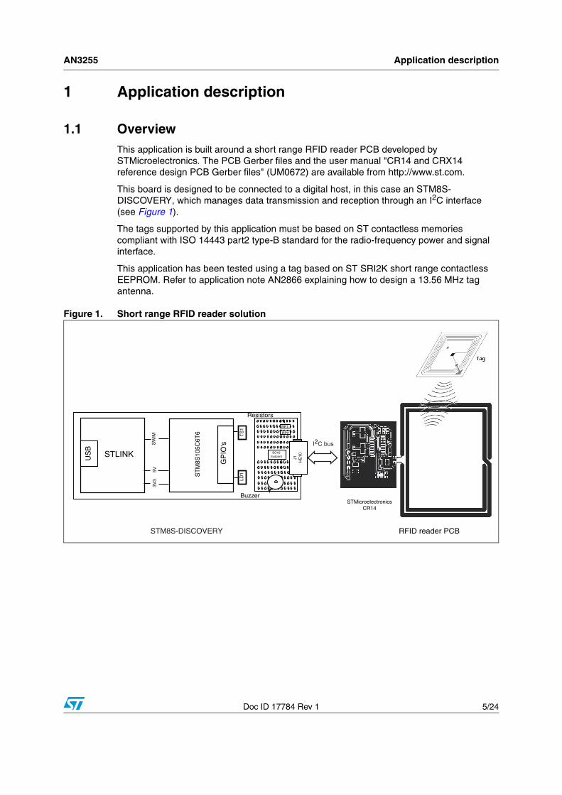
1.1 OverviewThis application is built around a short range RFID reader PCB developed by STMicroelectronics. The PCB Gerber files and the user manual "CR14 and CRX14 reference design PCB Gerber files" (UM0672) are available from http://www.st.com.
This board is designed to be connected to a digital host, in this case an STM8S-DISCOVERY, which manages data transmission and reception through an I2C interface (see Figure 1).
The tags supported by this application must be based on ST contactless memories compliant with ISO 14443 part2 type-B standard for the radio-frequency power and signal interface.
This application has been tested using a tag based on ST SRI2K short range contactless EEPROM. Refer to application note AN2866 explaining how to design a 13.56 MHz tag antenna.
Figure 1. Short range RFID reader solution
US
B
STLINK
SW
IM3V
35V
GP
IO's
LD1
TS
1
ST
M8S
105C
6T6
SO16footprint J1
HE
10
RP1
RP2
Buzzer
Resistors
RFID reader PCB
STMicroelectronicsCR14
I2C bus
STM8S-DISCOVERY
Application description AN3255
6/24 Doc ID 17784 Rev 1
1.2 Short-range contactless communication principles
1.2.1 CR14 contactless coupler
The CR14 is the main component of the RFID reader PCB. It interfaces with the following components:
● The contactless tags
The data frames exchanged with the tags are compliant with ISO14443 type-B radio frequency protocol. Data are stored in the CR14 input/output Frame registers (see Table 1: CR14 control registers).
● The STM8S105C6T6 through the I2C bus.
The CR14 is organized as 4 functional blocks:
● The I²C bus controller
It handles the serial connection with the STM8S105C6 application host, and controls the read/write accesses to all CR14 registers. It is compliant with the 400 KHz I2C bus specification.
● The RAM buffer
The RAM buffer is bidirectional. It stores all the request frame bytes to be transmitted to the tag, plus all the received bytes sent back by the tag on the answer frame.
● The transmitter
It powers the tag by generating a 13,56 MHz signal on an external antenna. The resulting field is 10% modulated using ASK (amplitude shift keying) modulation to transmit data.
● The receiver
It demodulates the signal generated on the antenna by the load variation of the tag. The resulting signal is decoded by an 847 KHz BPSK (binary phase shift keying) sub-carrier decoder.
The CR14 generates an electromagnetic field which is rectified to power the tag. The reader transmits information to the tag by modulating the carrier wave. To transmit information back to the reader, the tag backscatters the carrier wave by modifying its own impedance thereby perturbing the field.
The CR14 chip contains six volatile registers of which three allow to configure the CR14 and to transmit/receive frames to/from the tag (see Table 1):
● Parameter register
● Input/Output Frame register
● Slot Marker register
For details regarding registers description and CR14 I2C protocol, refer to the CR14 datasheet.
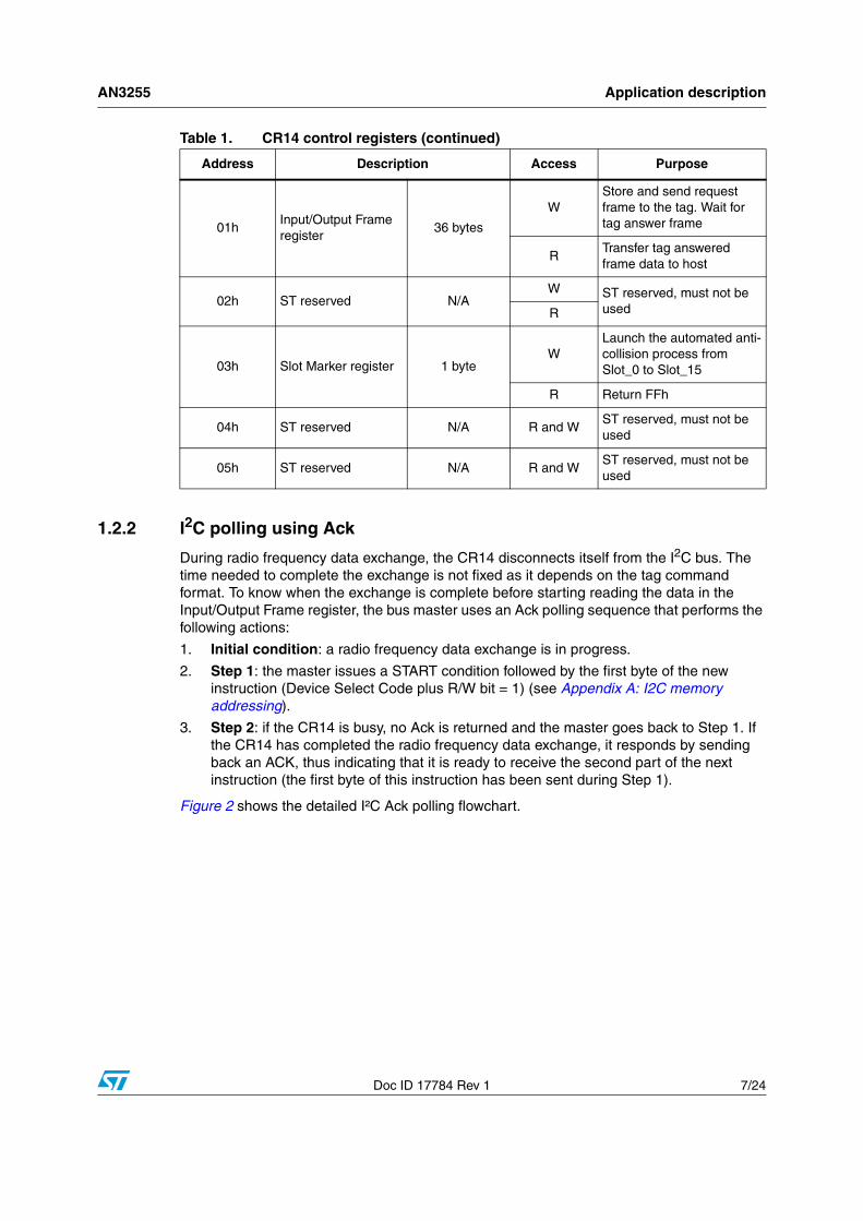
Table 1. CR14 control registers
Address Description Access Purpose
00h Parameter register 1 byteW Set parameter register
R Read parameter register
AN3255 Application description
Doc ID 17784 Rev 1 7/24
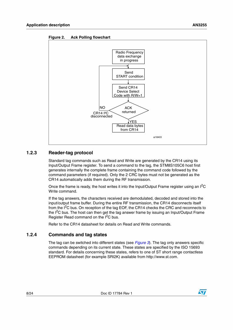
1.2.2 I2C polling using Ack
During radio frequency data exchange, the CR14 disconnects itself from the I2C bus. The time needed to complete the exchange is not fixed as it depends on the tag command format. To know when the exchange is complete before starting reading the data in the Input/Output Frame register, the bus master uses an Ack polling sequence that performs the following actions:
1. Initial condition: a radio frequency data exchange is in progress.
2. Step 1: the master issues a START condition followed by the first byte of the new instruction (Device Select Code plus R/W bit = 1) (see Appendix A: I2C memory addressing).
3. Step 2: if the CR14 is busy, no Ack is returned and the master goes back to Step 1. If the CR14 has completed the radio frequency data exchange, it responds by sending back an ACK, thus indicating that it is ready to receive the second part of the next instruction (the first byte of this instruction has been sent during Step 1).
Figure 2 shows the detailed I²C Ack polling flowchart.
01hInput/Output Frame register
36 bytes
WStore and send request frame to the tag. Wait for tag answer frame
RTransfer tag answered frame data to host
02h ST reserved N/AW ST reserved, must not be
usedR
03h Slot Marker register 1 byteW
Launch the automated anti-collision process from Slot_0 to Slot_15
R Return FFh
04h ST reserved N/A R and WST reserved, must not be used
05h ST reserved N/A R and WST reserved, must not be used
Table 1. CR14 control registers (continued)
Address Description Access Purpose
Application description AN3255
8/24 Doc ID 17784 Rev 1
Figure 2. Ack Polling flowchart
1.2.3 Reader-tag protocol
Standard tag commands such as Read and Write are generated by the CR14 using its Input/Output Frame register. To send a command to the tag, the STM8S105C6 host first generates internally the complete frame containing the command code followed by the command parameters (if required). Only the 2 CRC bytes must not be generated as the CR14 automatically adds them during the RF transmission.
Once the frame is ready, the host writes it into the Input/Output Frame register using an I2C Write command.
If the tag answers, the characters received are demodulated, decoded and stored into the input/output frame buffer. During the entire RF transmission, the CR14 disconnects itself from the I2C bus. On reception of the tag EOF, the CR14 checks the CRC and reconnects to the I2C bus. The host can then get the tag answer frame by issuing an Input/Output Frame Register Read command on the I2C bus.
Refer to the CR14 datasheet for details on Read and Write commands.
1.2.4 Commands and tag states
The tag can be switched into different states (see Figure 3). The tag only answers specific commands depending on its current state. These states are specified by the ISO 15693 standard. For details concerning these states, refers to one of ST short range contactless EEPROM datasheet (for example SRI2K) available from http://www.st.com.
AN3255 Application description
Doc ID 17784 Rev 1 9/24
Figure 3. TAG state transition diagram
1.3 Hardware requirementsThe following STM8S-DISCOVERY on-board resources are used:
● LED LD1
Refer Table 2, Table 3, Table 4, and Table 5 for the list of additional hardware required to make this application software run on the STM8S-DISCOVERY.
Power-off
Ready
Inventory
Selected
Deselected Desactivated
Chip_ID8bits = RND
Select(Chip_ID)Read_block()Write_block()Get_UID()
Completion()
Select(Chip_ID)
Selct( != Chip_ID)
Select(Chip_ID)
Reset_to_inventory()
Initiate() or Pcall16()or Slot_marker(SN) orSelect(wrong Chip_ID)
Initiate()
On fieldOut offield
Out offield
Out offield Out of
field
Out offield
ai18400
Table 2. List of PCB passive components
Component description Value Comment
Resistors
R1 N/A
Hardwired addressing of the CR14 (bits b3, b2, and b1 of the
7-bit I2C Device Select Code.Allow up to 7 CR14 readers to be addressed on the same I2C
bus
R2 0 Ω
R3 N/A
R4 0 Ω
R5 N/A
R6 0 Ω
R7 0 Ω -
Application description AN3255
10/24 Doc ID 17784 Rev 1
R8 0 ΩSerial resistor allowing to fine tune the quality factor of the
reader antenna
Capacitor
C1, C2 7 pF crystal oscillator capacitors
C3 22 nF -
C4 22 μF -
C5 5 pF (50 V) -
C6 100 nF -
C7, C7’ 220 pF (50 V), 56 pF (50 V)Capacitors allowing to fine tune
the RLC resonant frequency
C8, C8’ 82 pF (50 V), 22 pF (50 V)impedance adaptation of the
RLC resonant circuit.
Diode
D1 (N4148) Optional
Ferrite
L3,L4,L5,L6, L7 multilayer SMD ferrites
Removal of parasites for tag data reception and I2C
Table 3. List of PCB packaged components
Part name Component name Description Package
CR14/CRX14Short-range RFID
couplers
Contactless coupler compliant with short-
range ISO14443 type-B standard
SO16
13.56 MHz crystal CrystalGenerates a 13.56 MHz
carrier frequencyXTALCMS
Table 4. List of tag packaged components
Part name Component name Description Package
SRI2K13,56 MHZ short-range
contactless memory chip
Short-range contactless memory used to build a
tagSBN18
Table 5. List of other passive components
Component description Value Comment
Resistor
RP1, RP2 resistors 4,7 KΩ Pull-up for I2C open-drain
Table 2. List of PCB passive components (continued)
Component description Value Comment
AN3255 Application description
Doc ID 17784 Rev 1 11/24
1.4 Application schematicsFigure 4 shows the contactless reader implementation schematics. The reader is made of two parts:
● STMicroelectronics RFID reader PCB based on the CR14 short range contactless coupler (see Section 1.2.1).
● The STM8S-DISCOVERY which STM8S105C6T6 microcontroller controls the bidirectional communications with the CR14 through the I2C serial bus (refer to the CR14 datasheet).
Other
Piezo buzzer 5 V operating voltage Supports 4 KHz input frequency
Table 5. List of other passive components (continued)
Component description Value Comment
Application description AN3255
12/24 Doc ID 17784 Rev 1
Figure 4. Contactless RFID reader schematics
Vre
f1
RF IN
2E0
3E1
4E2
5G
ND
6G
ND
7G
ND
8SD
A9
SCL
10G
ND
11O
SC2
12O
SC1
13G
ND
_RF
14RF
OU
T15
VCC
16U
1
CRX
14
X1
C1C3 22
nF50
V
C8
C8'
C7C7
'
VCC
VCC
C6
+C4
L4 WU
RTH
742
-792
-042
L5 WU
RTH
742
-792
-042
L6 WU
RTH
742
-792
-042
L7WU
RTH
742
-792
-042
R7
R8
R1OPT
AN
T1
AN
T2
E0E1
E2
SCL
SDA
1234 J1
R2
R3OPT
R4
R5OPT
R6
VCC
D1
1N41
48 (O
PTIO
NA
L)
C5
L3 WU
RTH
742
-792
-042
Vre
f1
RF IN
2E0
3E1
4E2
5G
ND
6G
ND
7G
ND
8SD
A9
SCL
10G
ND
11O
SC2
12O
SC1
13G
ND
_RF
14RF
OU
T15
VCC
16U
1
X1
13.5
6 M
Hz
C17
pF 5
0 V
C27
pF 5
0 V
C3 22nF
50V
C882
pF
50 V
C8' 22
pF
50 V C7
220
pF 5
0 V
C7' 56 p
F 50
V
VCC
ant
VCC
ant
C6
100
nF 5
0 V
+C4 22
μF
10V
L4 WU
RTH
742
-792
-042
L5 WU
RTH
742
-792
-042
L6 WU
RTH
742
-792
-042
L7WU
RTH
742
-792
-042
R7
R8
R1OPT
AN
T1
AN
T2
E0E1
E2
SCL
SDA
1234
R20 Ω
R
R3OPT
R4
R5OPT
R6
VCC
ant
D1
1N41
48 (O
PTIO
NA
L)
C5 10 p
F 50
V
L3 WU
RTH
742
-792
-042
STM
8S
I²C
PD0
VCC
VCC
Buzz
erPi
ezo
PD4
PE1/
SCL
PE2/
SDA
VCC
VCC
BEEP
Rp1
Rp2
GN
Dan
t
GN
Dan
t
GN
Dan
t
GN
Dan
t
GN
Dan
t
GN
Dan
t
GN
Dan
t
GN
Dan
t
LD1
(gre
en)
0 Ω
R0
ΩR
0 Ω
R0 Ω
R
4,7�
Ω
4,7�
Ω
RFI
D re
ader
PC
B
AN3255 Application description
Doc ID 17784 Rev 1 13/24
The efficiency of data transfers between the RFID reader and tag depends on the tuning of their respective antenna. This is done by adjusting the following components:
● CS is the serial capacitance used to adapt the impedance of the reader antenna RLC equivalent circuit:
CS = C8 + C8’
● CP is the parallel capacitance used to tune the resonant frequency of the reader RLC equivalent circuit:
CP = C7 + C7’
● RS is the serial resistor used to fine tune the quality factor of the reader RLC resonant equivalent circuit:
RS = R8
Refer to application note AN1806 for details on how to design a reader antenna and infer the values of CP, CS and RS. This document is associated with a software tool using the Grover method to calculate the inductance of rectangular planar antennas.
Warning: The values of CS, CP, and RS are dependant. Tuning one of them impacts the 2 others. The best compromise must be found to achieve a good tuning for the reader antenna (refer to AN1806).
STM8S-DISCOVERY configuration AN3255
14/24 Doc ID 17784 Rev 1
2 STM8S-DISCOVERY configuration
2.1 Power supply configurationThe CR14 of the RFID reader PCB must be supplied from 5 V± 500 mV. This board being powered from STM8S-DISCOVERY VDD, the jumper JP1 of the STM8S-DISCOVERY must be set to VDD = 5 V (see UM0817).
2.2 Option byte configurationThe STM8S105C6T6 Beeper output is enabled through the alternate function remapping option (AFR7) of the OPT2 option byte:
AFR7 = 0: port D4 alternate function is TIM2_CH1 (default)
AFR7 = 1: port D4 alternate function is BEEP (required)
For details on the option byte and alternate function remapping, refer to UM0834 and to the STM8S105xx datasheet, respectively.
AN3255 Software description
Doc ID 17784 Rev 1 15/24
3 Software description
3.1 STM8S peripherals used by the applicationThe application software uses STM8S standard firmware library to control general purpose functions. These peripheral functions are the following:
● Clock (CLK)
The clock control enables and delivers the correct clock frequency to the CPU and peripherals. It configures the HSI prescaler division factor to 4. The I2C input clock frequency is 4 MHz to be able to generate correct timings compliant with Fast mode.
● GPIOs
They drive the MCU I/Os to interface with external hardware. They configure PD0 port as output push-pull high to drive LD1 and switch it off at initialization. PD4 port is configured through alternate function remapping to enable the Beeper output pin.
● I2C
This peripheral handles the serial connection with the CR14 contactless coupler of the RFID reader board. It controls the read/write access to the CR14 registers.
● Auto wake-up (AWU)
This peripheral is used to provide an internal wake-up timebase that is used when the MCU goes into Active-halt power saving mode. It is configured to wake up the MCU after 512 ms, which is a good trade-off between the time during which the microcontroller remains in Active-halt power saving mode and the time required by the RFID reader to identify the tag.
● Beeper
This peripheral drives the Beeper output pin with a signal of 4 KHz for sound generation.
● TIM3
The TIM3 timer is used to measure the LSI frequency with Input Capture 1 to reach with a better accuracy the standard Beeper frequency outputs.
3.2 Configuring the STM8S standard firmware library The stm8s_conf.h file of the STM8S standard firmware library is used to configure the library by enabling the peripherals used by the application.
The following define statements must be present:
#define _CLK 1 enables the clock control (CLK),#define _GPIO 1 enables the GPIOs,#define _I2C 1 enables the I2C interface,#define _AWU 1 enables the Auto wake-up,#define _BEEP 1 enables the beeper,#define _TIM3 1 enables timer 3.
Software description AN3255
16/24 Doc ID 17784 Rev 1
3.3 Application principleThis application initiates communications with the tags present in the range of the electromagnetic field generated by the reader antenna, and read the tag UIDs. If the operation succeeds, the STM8S105C6T6 emits a beep and blinks LD1.
When running the code in debug mode from STVD development tool, the UID value can be displayed in the Watch windows.
The application uses the I2C protocol to configure the CR14 embedded on the RFID reader board, and to transmit/receive frames to/from the tags (see Table 6). Communications with the tags are managed by the state transition diagram shown in Figure 3.
A possible way to improve this application would be to use an LCD screen to display the tag unique identifier (UID). Another improvement could be to implement the CR14 anti-collision capability which allows the reader to select up to 16 tags (one at a time) during predefined time slots.
Refer to Figure 5 for the flowchart of the application software main loop.
Table 6. TAG commands used within this application
Tag commands Description
Initiate() To detect if a tag in Ready state is present in the reader field range
Select(Chip_ID) Allow the tag to enter the Selected state
Get_UID() On receiving this command, the tag returns its 8 UID bytes
AN3255 Software description
Doc ID 17784 Rev 1 17/24
Figure 5. Main application loop flowchart
During peripheral initialization, the application first configures the CR14 parameter register to generate the 13,56 MHz RF field on the reader antenna.
Prior to issuing a Read/Write command (such as Get_UID()) to the memory tag, the tag state machine must be put in the Selected state by sending a Select(Chip_ID) command. All commands sent to the tag before this command is issued are ignored.
Once the peripheral initialization has completed, the application code enters a loop in which it checks if a tag is present in the RF field by writing periodically the Initiate() command in the CR14 Input/Output Frame register (see Appendix A: I2C memory addressing). If no tag is present in the electromagnetic field, the STM8S105C6T6 enters the Active-halt power saving mode for 512 ms and automatically wakes up to issue a new Initiate() command.
As soon as a tag is present in the electromagnetic field, it automatically enters the Ready state in which its 8-bit random Chip_ID is initialized. When receiving the Initiate() command, the tag then switches to the Inventory state in which its new 8-bit Chip_ID random value is set and returned to the CR14. Since this application software does not implement the anti-
Software description AN3255
18/24 Doc ID 17784 Rev 1
collision mechanism, the Chip_ID is stored by the host and sent as parameter to the Select(Chip_ID) command issued by the host to the tag. The tag then switches directly to the Selected state.
The Get_UID() command is then sent to the tag that answers by returning its 8 UID bytes. The host emits a beep and lights LD1 for about 1 s.
AN3255 I2C memory addressing
Doc ID 17784 Rev 1 19/24
Appendix A I2C memory addressing
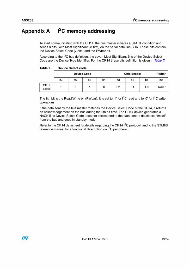
To start communicating with the CR14, the bus master initiates a START condition and sends 8 bits (with Most Significant Bit first) on the serial data line SDA. These bits contain the Device Select Code (7 bits) and the RWbar bit.
According to the I2C bus definition, the seven Most Significant Bits of the Device Select Code are the Device Type Identifier. For the CR14 these bits definition is given in Table 7.
The 8th bit is the Read/Write bit (RWbar). It is set to ‘1’ for I2C read and to ‘0’ for I2C write operations.
If the data sent by the bus master matches the Device Select Code of the CR14, it returns an acknowledgement on the bus during the 9th bit time. The CR14 device generates a NACK if its Device Select Code does not correspond to the data sent. It deselects himself from the bus and goes in standby mode.
Refer to the CR14 datasheet for details regarding the CR14 I2C protocol, and to the STM8S reference manual for a functional description on I2C peripheral.
Table 7. Device Select code
Device Code Chip Enable RWbar
b7 b6 b5 b4 b3 b2 b1 b0
CR14 select
1 0 1 0 E2 E1 E0 RWbar
I2C Read and Write functions AN3255
20/24 Doc ID 17784 Rev 1
Appendix B I2C Read and Write functions
This section gives an overview of the main functions controlling the read and write accesses to the CR14.
AN3255 I2C Read and Write functions
Doc ID 17784 Rev 1 21/24
B.1 I2C Page Write flowchartThe Page Write function performs write accesses to the CR14 registers. Its parameters are the buffer containing the bytes to be written to the CR14, the CR14 write address and the number of bytes to be written.
Figure 6 shows the detailed flowchart of the I2C_Page_Write function.
Figure 6. I2C Page Write flowchart
Start
I²C bus busy ?YES
NO
Send START condition
START conditiongenerated ?
YES
NO
Send CR14 Device Select Code
with R/W=0
END of Addresstransmission ?
Send registerwrite address
Data byte transfersucceeded ?
Number of datato be written > 0 ?
Send Data byte
Data byte transfersucceeded ?
GenerateSTOP condition
END
NO
YES
NO
YES
YES NO
Number of datato be written --
ai18402
I2C Read and Write functions AN3255
22/24 Doc ID 17784 Rev 1
B.2 I2C post polling buffer read flowchartThis function has been implemented to be used together with the I2C polling function. Once an ACK has been returned by I2C_CR14_EE_AckPolling, the I2C_CR14_EE_PostPolling function reads one by one all the bytes that are available in the Input/ Output Frame register of the CR14.
Figure 7 shows the detailed flowchart of the I2C_CR14_EE_PostPolling function.
Figure 7. I2C post polling buffer read flowchart
AN3255 Revision history
Doc ID 17784 Rev 1 23/24
Revision history
Table 8. Document revision history
Date Revision Changes
12-Oct-2010 1 Document migrated from UM0927 rev 1.
AN3255
24/24 Doc ID 17784 Rev 1
Please Read Carefully:
Information in this document is provided solely in connection with ST products. STMicroelectronics NV and its subsidiaries (“ST”) reserve theright to make changes, corrections, modifications or improvements, to this document, and the products and services described herein at anytime, without notice.
All ST products are sold pursuant to ST’s terms and conditions of sale.
Purchasers are solely responsible for the choice, selection and use of the ST products and services described herein, and ST assumes noliability whatsoever relating to the choice, selection or use of the ST products and services described herein.
No license, express or implied, by estoppel or otherwise, to any intellectual property rights is granted under this document. If any part of thisdocument refers to any third party products or services it shall not be deemed a license grant by ST for the use of such third party productsor services, or any intellectual property contained therein or considered as a warranty covering the use in any manner whatsoever of suchthird party products or services or any intellectual property contained therein.
UNLESS OTHERWISE SET FORTH IN ST’S TERMS AND CONDITIONS OF SALE ST DISCLAIMS ANY EXPRESS OR IMPLIEDWARRANTY WITH RESPECT TO THE USE AND/OR SALE OF ST PRODUCTS INCLUDING WITHOUT LIMITATION IMPLIEDWARRANTIES OF MERCHANTABILITY, FITNESS FOR A PARTICULAR PURPOSE (AND THEIR EQUIVALENTS UNDER THE LAWSOF ANY JURISDICTION), OR INFRINGEMENT OF ANY PATENT, COPYRIGHT OR OTHER INTELLECTUAL PROPERTY RIGHT.
UNLESS EXPRESSLY APPROVED IN WRITING BY AN AUTHORIZED ST REPRESENTATIVE, ST PRODUCTS ARE NOTRECOMMENDED, AUTHORIZED OR WARRANTED FOR USE IN MILITARY, AIR CRAFT, SPACE, LIFE SAVING, OR LIFE SUSTAININGAPPLICATIONS, NOR IN PRODUCTS OR SYSTEMS WHERE FAILURE OR MALFUNCTION MAY RESULT IN PERSONAL INJURY,DEATH, OR SEVERE PROPERTY OR ENVIRONMENTAL DAMAGE. ST PRODUCTS WHICH ARE NOT SPECIFIED AS "AUTOMOTIVEGRADE" MAY ONLY BE USED IN AUTOMOTIVE APPLICATIONS AT USER’S OWN RISK.
Resale of ST products with provisions different from the statements and/or technical features set forth in this document shall immediately voidany warranty granted by ST for the ST product or service described herein and shall not create or extend in any manner whatsoever, anyliability of ST.
ST and the ST logo are trademarks or registered trademarks of ST in various countries.
Information in this document supersedes and replaces all information previously supplied.
The ST logo is a registered trademark of STMicroelectronics. All other names are the property of their respective owners.
Australia - Belgium - Brazil - Canada - China - Czech Republic - Finland - France - Germany - Hong Kong - India - Israel - Italy - Japan - Malaysia - Malta - Morocco - Philippines - Singapore - Spain - Sweden - Switzerland - United Kingdom - United States of America