Page 1
1
BULENT ECEVIT UNIVERSITY
DEPARTMENT OF ELECTRICAL AND ELECTRONICS ENGINEERING
EXPERIMENT BOOK
PREPARED BY:
Asst. Prof. Rukiye UZUN
Res. Asst. Ali NARİN Res. Asst. İrem ŞENYER
ZONGULDAK, 2017
Page 2
2
PREFACE
This prepared notes include the application to be done in parallel with course topics of
Electronic-II in the third grade students in Electrical and Electronics Engineering.
Preparations of studies are realized on Multisim, Simulink, Proteus or PSpice simulation
program. Then, the values obtained are compared with laboratory studies. For each experiment
the students are required to prepare the report in accordance with the rules of reporting. Reports
prepared for this purpose:
A cover page will be and on it there will be the course name, application number, group
number and group member‘s signatures.
There will be an aim of the report and the work will be clearly stated.
The results obtained in the experiment will be given.
In the conclusion, the results interpreted.
All reports (tables, graphs) to be prepared by hand.
Page 3
3
TABLE OF CONTENTS
EXPERIMENT 1: Series And Parallel Voltage Regulators
EXPERIMENT 2: Double stage amplifier circuit
EXPERIMENT 3: The inverting amplifier and the non-inverting amplifier
EXPERIMENT 4: The summing amplifier and the difference amplifier
EXPERIMENT 5: The differentiatoras circuit
EXPERIMENT 6: The instrumentation amplifier circuit.
EXPERIMENT 7: Band-pass filter circuit.
EXPERIMENT 8: The square wave oscillator circuit with 555 IC.
Page 4
4
EXPERIMENT 1: Application Of Series And Parallel Voltage Regulators
AIM: The purpose of this experiment is to realize series and parallel volatge regulators circuits,
whose outputs are constant.
INTRODUCTION
One of the most important features for power supplies is that the changes in input voltage and
load connected to the output shouldn’t affect the output voltage. The process of holding fixed
the output voltage of power supplies is called regulation, used circuits for this purpose are
called the regulator circuits. In regulator circuits, Zener diode, transistor and integrated voltage
regulators are used.
1.1. Using of zener diode as voltage regulator
At the zener diode regulator, zener diode reverse voltage to a particular property, then taking
advantage of the turn. At the zener diode regulators, it is taking advantage of the characteristics
of zener diode starting to conduct after a particular reverse voltage. Zener diode is connected in
parallel with the load resistance in the opposite direction and when the load voltage pass a
particular value, thereby zener diode is conducting, then the current on the circuit increases.
This current increases the voltage drop on the series resitor connected the circuit, thus the load
voltage remains constant. Due to the structure of the zener diode, a fixed volatge arises even if
the voltage applied to the ends of zener diode is more than zener voltage. However to carry out
regulation of zener diode, it should be applied more voltage than zener voltage to the ends of
the zener diodes. Figure 1.1 shows a simple zener diode regulator circuit.
Figure 1.1 Using of zener diode as a volatge regulator.
Page 5
5
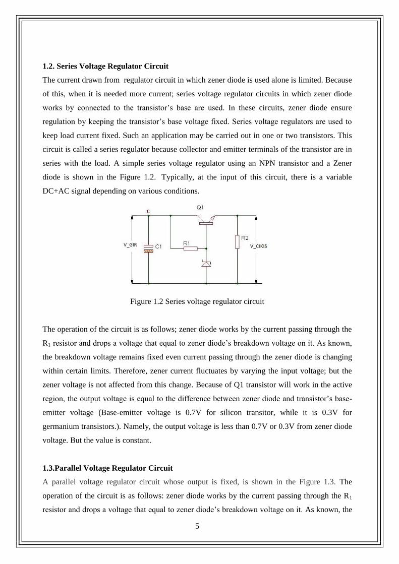
1.2. Series Voltage Regulator Circuit
The current drawn from regulator circuit in which zener diode is used alone is limited. Because
of this, when it is needed more current; series voltage regulator circuits in which zener diode
works by connected to the transistor’s base are used. In these circuits, zener diode ensure
regulation by keeping the transistor’s base voltage fixed. Series voltage regulators are used to
keep load current fixed. Such an application may be carried out in one or two transistors. This
circuit is called a series regulator because collector and emitter terminals of the transistor are in
series with the load. A simple series voltage regulator using an NPN transistor and a Zener
diode is shown in the Figure 1.2. Typically, at the input of this circuit, there is a variable
DC+AC signal depending on various conditions.
Figure 1.2 Series voltage regulator circuit
The operation of the circuit is as follows; zener diode works by the current passing through the
R1 resistor and drops a voltage that equal to zener diode’s breakdown voltage on it. As known,
the breakdown voltage remains fixed even current passing through the zener diode is changing
within certain limits. Therefore, zener current fluctuates by varying the input voltage; but the
zener voltage is not affected from this change. Because of Q1 transistor will work in the active
region, the output voltage is equal to the difference between zener diode and transistor’s base-
emitter voltage (Base-emitter voltage is 0.7V for silicon transitor, while it is 0.3V for
germanium transistors.). Namely, the output voltage is less than 0.7V or 0.3V from zener diode
voltage. But the value is constant.
1.3.Parallel Voltage Regulator Circuit
A parallel voltage regulator circuit whose output is fixed, is shown in the Figure 1.3. The
operation of the circuit is as follows: zener diode works by the current passing through the R1
resistor and drops a voltage that equal to zener diode’s breakdown voltage on it. As known, the
Page 6
6
breakdown voltage remains fixed even current passing through the zener diode is changing
within certain limits. The output voltage is equal to the summation of zener voltage and
transistor’ base-emitter voltage (Base-emitter voltage is 0.7V for silicon transitor, while it is
0.3V for germanium transistors.). Since the zener diode and base-emitter voltage are roughly
fixed values, the changes in the input voltage aren’t reflected at the output within certain limits
and a DC voltage is measured at the output.
Figure 1.3 Parallel voltage regulator circuits, whose output is fixed.
PRELIMINARY STUDY
1. Please implement experiment study one by one with simulation programs.
2. Please indicate the differences between series voltage regülatör and parallel voltage
regülatör
3. where is series voltage regülatör and parallel voltage regülatör used.
MATERIAL LIST
Resistors: 2x220Ω, 1x3.3kΩ, 1x100Ω, 1x50Ω, 1x270Ω, 1x540Ω,
Zener Diode: 12V,3V
Transistor: 2N2222A Si transitor or its compelent.
EXPERIMENT STUDY:
PART 1:
I. Examination of the series voltage regulator whose output is constant, while it is
unloaded:
1. Set the circuit shown in Figure 1.4. Set the values of the voltage source shown in Table
1.1 and write down the appropriate place by measuring the output voltage and VCE for each
value. record the appropriate place.
Page 7
7
Warning: This circuit is not short-circuit protected. For this reason, make sure not to short the
output. Otherwise, the transistor may be corrupted. (R1=3.3KΩ, 12V Zener diode)
Figure 1.4
Table 1.1
V_GIR (DC) V_CIKIS (V) VCE (V)
13V
15V
18V
21V
2. From the Table 1.1:
a) Input voltage 15 to 25 volts, then the output voltage varies between how much has
changed? Giriş gerilimi 15-25 volt arasında değiştiği halde çıkış gerilimi ne kadar
değişmiştir?
b) In this case,does the circuit work as a voltage regulator, whose output is constant?
c) Where is the increase of the input is compensated while the output voltage is constant?
Describe briefly.
d) Why is the series regulator name given to this circuit? Explain.
II. Examination of the series electronic voltage regulator whose output is constant,
while it is loaded:
1. Set the circuit again shown in Figure 1.4 by connecting a 440Ω resistor (two 220Ω
resistors connect series to obtain a 440Ω resistor) between circuit output and ground. Set the
voltage source and load resistor given values at Table 1.2 and measure output voltage and load
current for each value.
Page 8
8
Warning: Load current will be calculated approximately.
Table 1.2
V_GIR (V) R2 (Ω) V_CIKIS (V) IRY (mA)
15 440
15 220
25 440
25 220
III. Comparison by examining of the series electronic voltage regulator whose output
is constant, while it is unloaded, low-loaded and loaded:
1. Set the input voltage as 20V at Figure 1.4. Measure the output voltage and VCE voltage
while it is unloaded. Then connect 270Ω ve 540Ω respectively, repeat the same measurements
and write down the results. According to the results;
a) According to results at Table 1.3, is there any difference between unloaded, low-
loaded and loaded cases? If yes, what could be the reason for the difference? Why? Explain.
Table 1.3
V_GIR (V) R2 (Ω) V_CIKIS
(V)
VCE (V) VZ (V)
20 unloaded
20 540
20 270
PART 2:
I. Examination of the parallel electronic voltage regulator whose output is constant,
while it is unloaded:
1. Set the circuit diagram shown in Figure 1.5 and apply 10V input. What is the function of
the R resistance on the circuit? Measure V_GIR, VR1,Vz, VBE and V_CIKIS. 3V zener diode will
be used in the circuit.
Page 9
9
Figure 1.5
a) Is V_GIR equal to V_CIKIS+VR1? Why?
b) Is V_CIKIS equal to Vz+VBE? Why?
2. Observe the output voltage for three values of the input voltage between 10V and 15V.
Does it change? Does the circuit work as a voltage regulator ?
3. Observe the same process for VR1. Does it change? According to this, where the value
of the input voltage is compensated?
II. Examination of the parallel electronic voltage regulator whose output is constant,
while it is loaded:
1. Connect the load (220Ω) between the ground and the output of the circuit in Figure 1.5
and ground. The power supply output must be 10V. Observe the output voltage. Does the
output change if the load is connected to circuit or not? the absence of the load? To what
degree?
RESULTS AND COMMENTS
1. Report all processes and measurements made in the experimental part. Add answer of
the question that asked at the experiment part into the your comments.
2. Compare the measurements of the circuit by theoretical calculations.
Page 10
10
EXPERIMENT 2: Double Stage Amplifier Circuit
AIM: Examine double stage amplifier circuit.
PRELIMINARY STUDY
1. Please implement experiment study one by one with simulation programs.
2. How to obtain the gain frequency curve? How to determine the lower and upper corner
frequency?
MATERIAL LIST
Resistors: 220 Ω, 330 Ω, 220 Ω, 680 Ω, 820 Ω, 1 kΩ, 2x5.6 kΩ, 2x10 kΩ, 2x56 kΩ, 1x100 kΩ
Condansator: 3x2.2 µF, 2x10 µF
Transistor: 2xBC107 veya 2x2N3904
EXPERIMENT STUDY:
1. Set the following two multi stage amplifier (CE+CE) circuit.
2. Measure base, emitter and collector DC voltages of the transistors using an electronic
voltmeter.
3. Calculate 𝐼𝐶 , 𝐼𝐸 ve 𝐼𝐵 currents and 𝑉𝐵𝐸 , 𝑉𝐶𝐸 voltages and 𝛽𝑑𝑐 current gains.
4. For 𝑉𝑆 = 30 𝑚𝑉; obtain the gain curve of the circuit for the frequencies between 50 Hz
– 5 MHz.
5. Find the lower and upper corner frequency of the circuit.
Page 11
11
6. How much is the amount of attenuation of the gain curve at the low and high
frequencies?
RESULTS AND COMMENTS
Report all processes and measurements made in the experimental part. Please add your
comments.
Page 12
12
EXPERIMENT 3: İnverting Amplifier and Non-İnverting Amplifier Circuits
AIM: Examine inverting amplifier and non-inverting amplifier as an application of the op-amp.
INTRODUCTION:
Today, one of the key structures used in the field of analog electronics is operational
amplifier (op-amp-Operational Amplifiers) that was first developed for use in analog
calculation process. Today, it is being used commonly at all the low-frequency applications,
particularly measurement, automatic control, analog / digital and digital / analog converters
being used as common. The basic logic of the op-amp is very simple and it can be performed
many functions through these simple logic.
At an ideal op-amps, voltage gain is infinite, input resistance is infinite, output resistance is
zero and can be applied at any feedback, namely they are an absolute stable amplifier. Voltage
gain of a non-ideal opamp is very high and may be different values. Depending on the types,
voltage gains are between ten thousand and a million, but it can be found in more gainful ones.
Opamp’s input resistance is quite high, while their output resistance is small between 1 and
1000 Ohm. Limits of the frequency are increasing from DC up to GHz levels.
There are approximately 30 transistors, 10 resistors and a few pieces diodes within an op-
amp.Their structure is a shape of as semiconductor integrated, also their volume is small and
their cost is low. Their power losses is low and since they are stable, they can be used in a large
number of highly complex systems. Figure 3.1 shows circuit symbol of an ideal opamp with an
equivalent circuit and with a physical connection.
Ideal op-amp:
ip = 0, in = 0, Vp= Vn
b) Small-signal equivalent of the opamp
formed by dependent voltage source and
resistors
a) Op-amp circuit symbol
Page 13
13
c) LM741 Physical connections of the op-amp circuit.
Figure 3.1 Op-amp’s symbol and its small-signal equivalent and physical schema.
There are two inputs of op-amp circuit, one of them is marked by (+) and the other is
marked by (-). The signal applied to the (+) input is at the same phase with the output, while the
signal applied to the (-) input is at the 180 degree reverse phase.
Same signal applied to the two input will not be transferred to the output. (-) input is called
“(inverting)’’, while (+) input is called “non-inverting”. The characteristics of the circuit
depend on which end is used as the input and the amount of feedback from the output to input.
Inverting Amplifier:
Figure 3.2
Structure of a phase inverting amplifier (negative gain amplifier) can be seen in Figure 2.2.
assuming that current of the op-amp input is zero, if the Kirchoff's currents law is writen for
negative terminal (pin number 2):
𝐼𝑅1 + 𝐼𝑅2 = 0
Page 14
14
When these currents are expressed in terms of resistance and voltage values, then these
equation is obtained:
𝑉𝑖𝑛 − 𝑉𝑛
𝑅1+
𝑉𝑜𝑢𝑡 − 𝑉𝑛
𝑅2= 0
From here the output voltage is:
𝑉𝑜𝑢𝑡 = −(𝑉𝑖𝑛
𝑅1)𝑅2
Thus the voltage gain of the inverting amplifier is equal to the rate of −𝑅1
𝑅2. (-) sign in front of
the expression shows the phase difference of 1800 between inverting amplifier input and output.
The input resistance of the inverting amplifier is equal to R1 resistance. Also the output
resistance is very low and it is inverse proportion with Av.
If R2 is equal to R1, in this case the circuit gain is 1. Such a circuit is usually used when it is
wanted to change of a signal polarity.
Figure 3.3
By varying the resistance value of R2, as shown in Figure 3.3, it can be obtained a
controllable gain amplifier. Circuit gain will take different values according to the location of
the K commutator. Circuit gain of a non-feedback op-amp circuits is very high at frequencies of
DC and close to DC and approachs to 1 while frequency increases. This is presented in Figure
2.4 again.
Page 15
15
Figure 3.4
Usually, the gain of the op-amp circuits (Av, feedback gain), what should be the voltage
gains of them, and the desired bandwidth are determined From Figure 3.4 or similiar graphs.
Considering the safety allowance, Av is determined as 𝐴𝑣𝑜
10.
For example; if the bandwidth is wanted to be 10 kHz (with using 741 or 747 op-amp),
Avo is determined as 100 from Figure 3.4. According to this Av is equal to 100/10=10. In this
case If an amplifier with a bandwidth of 10kHz will be made by using 741 (or 747), the
resistors R1 and R2 must be selected so that the voltage gain of the amplifier is equal to 10.
Selection of R1 and R2 so that gain is much higher will be narrowed the band.
Non-İnverting Amplifier
Structure of a phase non-inverting amplifier (negative gain amplifier) can be seen in Figure 3.7.
Here the input signal is applied to the (+) terminal. The input is at the same phase with the
output. The circuit gain is expressed as follows;
𝐴𝑣 = 1 +𝑅2
𝑅1
Figure 3.5 Figure 3.6
Page 16
16
Figure 3.7
In this context, output resistance is quite high. Figure 3.8 is an equivalent shape of Figure 3.7.
Note that both of them is identical to each another.
Figure 3.8
The main differences between the inverting and non-inverting amplifiers are as follows. At
non-inverting amplifier, input and output is in the same phase, while there is an 1800 phase
difference between them at the inverting amplifier.
Input resistance of non-inverting amplifier is equal to the input resistance of the op-amp
and it is very high. Input resistance of inverting amplifier is equal R1.
The gain of non-inverting amplifier is excessive 1 from the gain of inverting amplifier and
always it is bigger than 1. There is no much difference between them in terms of other features
such as bandwidth, output resistance.
PRELIMINARY STUDY:
1. Please implement experiment study one by one with simulation programs.
2. Calculate the voltage gain and bandwidth for each experiment study.
Page 17
17
MATERIAL LIST
Resistors: 2x10KΩ, 1x100KΩ,1x33KΩ
Opamp: 741 veya 747
EXPERIMENT STUDY:
PART I:
1. Set the circuit shown in Figure 3.9. Here R2 will be 10KΩ.
Figure 3.9
2. (+) and (-) parts of the power source are setted to +12V and -12V, respectively.
3. Apply ±12 feed voltage in the circuit.
4. Set the output of the signal generator to a sinusoidal wave whose frequency is 1kHz and
amplitude is 2 V(t-t).
5. Apply the input signal to the A channel of the oscilloscope, also the output signal to the
B channel of the oscilloscope. Apply output of the signal generator to the input of the circuit.
a). Observe Vçk and Vgr signals on the oscilloscope screen, together. Are there a phase
difference between them? How much?
b). Find the voltage gain of the circuit and write down at Table 2.1
Table 3.1
R2 (KΩ) Vo Vi Av
10
33
100
Change R2 with 33 KΩ. In this case, what is the circuit gain? Write down at the Table 2.1.
6. Change R2 with100 KΩ. Find the circuit gain, then write down at the Table 3.1.
Page 18
18
7. When the results at the Table 3.1. is examined ,
a) Is |𝐴𝑣| =𝑅2
𝑅1 ?
b) Compare the results that find in preliminary study and in the experiment.
8. While R1= 10KΩ, R2=33KΩ, increase the frequency of the signal generator.
At which frequency the amplitude of the output signal decreases two-thirds of the
amplitude value of 1kHz frequency? Note this value (bandwidth of the amplifier) and compare
this with the results that is found in preliminary study. Are there any difference? Why?
PART II
1. Set the circuit shown in Figure 3.10. Here R2 will be 10kΩ.
Figure 3.10
2. (+) and (-) parts of the power source are setted to +12V and -12V, respectively.
3. Apply ±12 feed voltage in the circuit.
4. Set the output of the signal generator to a sinusoidal wave whose frequency is 1kHz and
amplitude is 2 V(t-t).
5. Apply the input signal to the A channel of the oscilloscope, also the output signal to the
B channel of the oscilloscope.
6. Apply output of the signal generator to the input of the circuit.
a). Observe Vçk and Vgr signals on the oscilloscope screen, together. Are there a phase
difference between them? How much?
b). Find the voltage gain of the circuit and write down at Table 3.1.
Page 19
19
Table 3.2
R2 (KΩ) AV
10
33
100
7. Change R2 with 33 KΩ. In this case, what is the circuit gain? Write down at the Table
3.1.
8. Change R2 with100 KΩ yapınız. Find the circuit gain, then write down at the Table 3.1.
9. When the results at the Table 2.1. is examined,
a) Is |𝐴𝑣| = 1 +𝑅2
𝑅1 ?
b) Compare the results that find in preliminary study and in the experiment.
10. Remember the results found for inveritng amplifier. Is the gain of non-inverting
amplifier exceed one from the gain of inverting amplifier under the same conditons?
11. While R1= 10KΩ, R2=33KΩ, increase the frequency of the signal generator.
At which frequency the amplitude of the output signal decreases two-thirds of the
amplitude value of 1kHz frequency? Note this value (bandwidth of the amplifier) and compare
this with the results that is found in preliminary study. Are there any difference? Why?
12. Remember the results found for inveritng amplifier. Do you observe that inverting and
non-inverting amplifiers have similar bandwidth at about the same voltage gains?
RESULTS AND COMMENTS
1. Report all processes and measurements made in the experimental part. Add answer of
the question that asked at the experiment part into the your comments.
2. Compare the measurements of the circuit by theoretical calculations.
Page 20
20
EXPERIMENT 4: Summing Amplifier and Difference Amplifier
AIM: Examine the summing amplifier and the difference amplifier as an application of the op-
amp.
INTRODUCTION
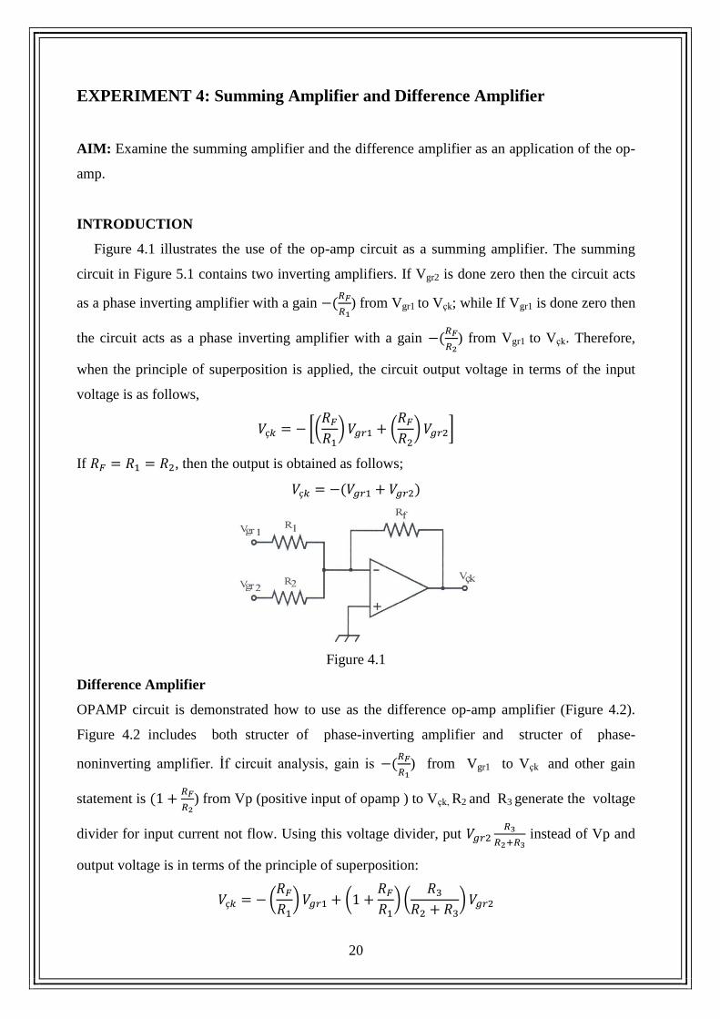
Figure 4.1 illustrates the use of the op-amp circuit as a summing amplifier. The summing
circuit in Figure 5.1 contains two inverting amplifiers. If Vgr2 is done zero then the circuit acts
as a phase inverting amplifier with a gain −(𝑅𝐹
𝑅1) from Vgr1 to Vçk; while If Vgr1 is done zero then
the circuit acts as a phase inverting amplifier with a gain −(𝑅𝐹
𝑅2) from Vgr1 to Vçk. Therefore,
when the principle of superposition is applied, the circuit output voltage in terms of the input
voltage is as follows,
𝑉ç𝑘 = − [(𝑅𝐹
𝑅1) 𝑉𝑔𝑟1 + (
𝑅𝐹
𝑅2) 𝑉𝑔𝑟2]
If 𝑅𝐹 = 𝑅1 = 𝑅2, then the output is obtained as follows;
𝑉ç𝑘 = −(𝑉𝑔𝑟1 + 𝑉𝑔𝑟2)
Figure 4.1
Difference Amplifier
OPAMP circuit is demonstrated how to use as the difference op-amp amplifier (Figure 4.2).
Figure 4.2 includes both structer of phase-inverting amplifier and structer of phase-
noninverting amplifier. İf circuit analysis, gain is −(𝑅𝐹
𝑅1) from Vgr1 to Vçk and other gain
statement is (1 +𝑅𝐹
𝑅2) from Vp (positive input of opamp ) to Vçk, R2 and R3 generate the voltage
divider for input current not flow. Using this voltage divider, put 𝑉𝑔𝑟2𝑅3
𝑅2+𝑅3 instead of Vp and
output voltage is in terms of the principle of superposition:
𝑉ç𝑘 = − (𝑅𝐹
𝑅1) 𝑉𝑔𝑟1 + (1 +
𝑅𝐹
𝑅1) (
𝑅3
𝑅2 + 𝑅3) 𝑉𝑔𝑟2
Page 21
21
If 𝑅𝑓 = 𝑅1 = 𝑅2 = 𝑅3, output is;
𝑉ç𝑘 = 𝑉𝑔𝑟2 − 𝑉𝑔𝑟1
Figure 4.2 Difference Amplifier
PRELIMINARY STUDY:
1. Please implement experiment study one by one with simulation programs.
2. How many volts are observed at the output of the circuit in Figure 4.3 observed?
Calculate.
3. Answer the same question for the circuit in Figure 4.4.
4. How many volts are the output of circuits observed in Figure 4.5? Calculate.
5. Answer the same question fort he circuit in Figure 4.6.
Figure 4.5 Figure 4.6
Figure 4.3 Figure 4.4
Page 22
22
MATERIAL LIST
Resistors: 4x10KΩ, 3x33KΩ, 1x2.2KΩ, 1x1KΩ, 1x5.6KΩ
Opamp: 741 veya 747
EXPERIMENT STUDY:
PART I
1. Set the circuit shown in Figure 4.7.
2. (+) and (-) parts of the power source are setted to +12V and -12V, respectively.
3. Apply ±12 feed voltage in the circuit. By using a digital multimeter;
a) Measure and write down Vgr1, Vgr2 ve Vçk voltages. Is 𝑉ç𝑘 = (𝑉𝑔𝑟1 + 𝑉𝑔𝑟2)?
b) Compare the results that find in preliminary study and in the experiment.
4. Change R2 with 33 KΩ. . By using a digital multimeter;
a) Measure and write down Vgr1, Vgr2 ve Vçk voltages. Is 𝑉ç𝑘 = (𝑉𝑔𝑟1 + 𝑉𝑔𝑟2)
equivalent valid? If not explain why?
b) Compare the results that find in preliminary study and in the experiment.
Figure 4.7
Page 23
23
PART II
1. Set the following circuit (Figure 4.8).
Figure 4.8
2. Respectively, adjust power supply (parts of (+) and (-)) +12 volts and -12 volts .
3. Apply ± 12 volt to circuit. Then, using digital multimeter:
a. Measure and save Vgr1, Vgr2 and Vçk voltage values. Does 𝑉ç𝑘 = (𝑉𝑔𝑟2 − 𝑉𝑔𝑟1)?
b. Compare these values with the result of preliminary study.
4. R3 = RF = 33KΩ. Using digital multimeter:
c. Again, Measure and save Vgr1, Vgr2 and Vçk voltage values.
𝑉ç𝑘 = (𝑉𝑔𝑟2 − 𝑉𝑔𝑟1) equality is still valid? If not, why? Explain.
d. Compare these values with the result of preliminary study.
RESULTS AND COMMENTS
1. Report all processes and measurements made in the experimental part. Add answer of
the question that asked at the experiment part into the your comments.
2. Compare the measurements of the circuit by theoretical calculations.
Page 24
24
EXPERIMENT 5: Differantial Circuit
AIM: Investigate differantial circuit as the application of op-amp.
INTRODUCTION:
In general, differantial circuits are a characteristic of the inverting amplifier (Figure 5.1).
Unlike, there is capacitor (Cgr) instead of the entrance resistance. Circuit derivatives to periodic
signal applied to its input and transfers to output. Briefly, this operation formulas, can be
explained as follows: Input empedance is very high, so, approximately x point voltage is 0V (+
point voltage). Current flow through the capacitor (Cgr).
𝑖𝑖𝑛 = 𝐶𝑔𝑟
𝑑𝑉𝑔𝑟
𝑑𝑡
Output voltage:
𝑉𝑜𝑢𝑡 = −𝑅𝑓𝑖𝑓
Because of 𝑖𝑓 = 𝑖𝑔𝑟, Output voltage:
𝑉ç𝑘 = −𝑅𝑓𝐶𝑔𝑟
𝑑𝑉𝑔𝑟
𝑑𝑡
Figure 5.1
Figure 5.1, İnput signal (Vgr) is derivated and then is transfered to output after multiplying with
a constant 𝑅𝑓𝐶𝑔𝑟. the circuit in Figure 5.1 is not sufficient in practice. because 𝐶𝑔𝑟 capacitor
acts as a short circuit at higher frequencies. So, gain increases. Output reaches high values for
these frequencies and noise occurs. To prevent noise and high frequencies, to put limits gain of
the op-amp circuit for the high frequency. 𝑅𝑔𝑟 is added (Figure 5.2), therefore, the problem is
Page 25
25
eliminated. So maximum gain of circuit is 𝑅𝑓/𝑅𝑔𝑟 . Two conditions must be provided in order
to operate differential circuits.
Figure 5.2
1. Input signal frequency:
𝑓𝑔𝑟 ≤1
2𝜋𝑅𝑔𝑟𝐶𝑔𝑟= 𝑓𝑐
signals with a frequency greater than this value will not work for the differential
circuits.
2. 𝑅𝑓𝐶𝑔𝑟 is named "time constant". Approximately, Input value should be around this
value.
Example: Does following circuit work as the differential circuits? (Figure 5.3)(f=1kHz).
Figure 5.3
Page 26
26
𝑓𝑔𝑟 ≤1
2𝜋𝑅𝑔𝑟𝐶𝑔𝑟=
1
2𝜋. 103. 0,1.10−6
𝑓𝑐 =104
2𝜋
In this case, 𝑓𝑔𝑟 < 𝑓𝑐. The time constant of the circuit:
𝑅𝑓𝐶𝑔𝑟 = 0,1.10−6. 10.103 𝑠𝑛 = 1𝑚𝑠𝑛
period of input signal:
𝑇𝑔𝑟 =1
𝑓𝑔𝑟=
1
1𝐾𝐻𝑧= 1 𝑚𝑠𝑛
as shown, period of input signal, is equal to the time constant of the circuit. Thus, the circuit
can operate at 1 KHz frequency as the differential circuits.
Now, 1 KHz frequency sinusoidal input and 0.5V input voltage is applied to investigate how
the signal to be seen as a signal of output.
𝑉𝑔𝑟 = 0,5. sin 2𝜋𝑓𝑡 = 0,5. sin 2𝜋(1000)𝑡
𝑉ç𝑘 = −𝑅𝑓𝐶𝑔𝑟
𝑑𝑉𝑔𝑟
𝑑𝑡
𝑉ç𝑘 = −(10𝐾Ω)(0,1𝜇𝐹)𝑑
𝑑𝑡(0,5 sin 2𝜋(1000)𝑡)
𝑉ç𝑘 = −(10𝐾Ω)(0,1𝜇𝐹)(0,5.2𝜋. 1000)(cos(2𝜋(1000)𝑡) = 3.14 cos 2𝜋(1000)𝑡
Thus, output signal is the cosine curve of 1 KHz frequency and 3.14 a peak value.
NOT: 𝑑
𝑑𝑡𝑠𝑖𝑛 2𝜋𝑓𝑡 = 2𝜋𝑓. 𝑐𝑜𝑠2𝜋𝑓𝑡
Page 27
27
PRELIMINARY STUDY:
1. Please implement experiment study one by one with simulation programs.
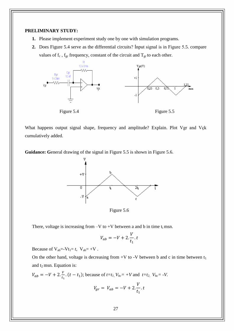
2. Does Figure 5.4 serve as the differential circuits? İnput signal is in Figure 5.5. compare
values of fc , fgr frequency, constant of the circuit and Tgr to each other.
Figure 5.4 Figure 5.5
What happens output signal shape, frequency and amplitude? Explain. Plot Vgr and Vçk
cumulatively added.
Guidance: General drawing of the signal in Figure 5.5 is shown in Figure 5.6.
Figure 5.6
There, voltage is increasing from –V to +V between a and b in time ti msn.
𝑉𝑎𝑏 = −𝑉 + 2.𝑉
𝑡1. 𝑡
Because of Vab=-Vt1= t, Vab= +V .
On the other hand, voltage is decreasing from +V to -V between b and c in time between t1
and t2 msn. Equation is:
𝑉𝑎𝑏 = −𝑉 + 2.𝑉
𝑡1. (𝑡 − 𝑡1); because of t=t1, Vbc= +V and t=t2, Vbc= -V.
𝑉𝑔𝑟 = 𝑉𝑎𝑏 = −𝑉 + 2.𝑉
𝑡1. 𝑡
Page 28
28
𝑉𝑐𝑘 = 𝑅𝐹𝐶𝑔𝑟
𝑑
𝑑𝑡(−𝑉 + 2.
𝑉
𝑡1. 𝑡) = −𝑅𝐹𝐶𝑔𝑟 (2
𝑉
𝑡1) = −2𝑅𝐹𝐶𝑔𝑟 (
𝑉
𝑡1)
𝑉𝑔𝑟 = 𝑉𝑏𝑐 = +𝑉 − 2.𝑉
𝑡1. (𝑡 − 𝑡1)
𝑉𝑐𝑘 = −𝑅𝐹𝐶𝑔𝑟
𝑑
𝑑𝑡(𝑉 − 2.
𝑉
𝑡1. (𝑡 − 𝑡1)) = −𝑅𝐹𝐶𝑔𝑟 (−2
𝑉
𝑡1) = 2𝑅𝐹𝐶𝑔𝑟 (
𝑉
𝑡1)
According to this, Vck signal is a square wave 𝑡ℎ𝑎𝑡 𝑖𝑠 𝑡𝑜 𝑏𝑒 2𝑅𝐹𝐶𝑔𝑟 (𝑉
𝑡1). In the light of this
information, Answer a preliminary study 2.
MATERIAL LIST
Resistors: 1x1KΩ, 1x10KΩ
Capacitor: 1x 10nF
Op-amp: 741 veya 747
EXPRIMENT STUDY:
1. Set the following circuit (Figure 5.7).
Figure 5.7
2. Adjust power supply +12 volts and -12 volts.
3. Adjust signal generator triangle wave that have 1 KHz frequency and 2 V ( Vp-p)
amplitude values.
Page 29
29
4. Apply A channel of the oscilloscope to input signal and B channel of the oscilloscope
to output signal. Both channels: frequency 1 kHz, amplitude 1 volt may be set to
display a sign in the best way.
5. Apply output of signal generator to circuit input.
a. Observe signals on the oscilloscope screen together with the Vgr ile Vçk. Is there a
phase difference between them? How much?
b. Measure peak value of Vçk . Compare this result with found the result that a
preliminary study 2.
6. The frequency of the triangle wave is 0.5 KHz. But, The amplitude of the triangle wave
is same (2 V ( Vp-p).
7. What changes are watching for output signal? How do you explain these changes?
8. The frequency of the triangle wave is 20 KHz. But, The amplitude of the triangle wave
is same (2 V ( Vp-p). How to exit signal has changed according to previous sisgnal?
Why? How much voltage gain of the circuit? Is this gain near to 𝐴𝑣 =𝑅𝐹
𝑅𝑔𝑟=
10𝐾
1𝐾= 10
? Why? Explain.
RESULTS AND COMMENTS
1. Please report all transactions and measurements. Please add your comments.
2. Compare all results by theoretical calculations of the circuit.
Page 30
30
EXPERIMENT 6: Instrumentation Amplifier
AIM: Examine Instrumentation Amplifier Circuits
PRELIMINARY STUDY:
1. Please implement experiment study one by one with simulation programs
2. Where are the areas of Instrumentation amplifier.
3. What are the advantages and disadvantages of instrumentation amplifier.
MATERIAL LIST
Resistor: 4x10 kΩ, 2x100 kΩ
Potansiyometer:1 kΩ
Op-amp: 3x741
EXPERIMENT STUDY
1. Set the following instrumentatıon amplifier circuit (Figure 7.1).
Figure 7.1
2. For 𝑉1 = 0 and 𝑉2 = 8 𝑚𝑉/1𝑘𝐻𝑧 ; observe the voltage 𝑉0 and 𝑉2 on the oscilloscope
and draw in the same time scale.
3. For 𝑉1 = 4𝑚𝑉/1𝑘𝐻𝑧 and 𝑉2 = 0; observe the voltage 𝑉0 and 𝑉1 on the oscilloscope
and draw in the same time scale.
4. Compare the results obtained at 1. and 2. Options.
5. Calculate the voltage gain according to the measurement results.
6. Obtain the formula of the voltage gain 𝐴𝑉 = 𝑉0/(𝑉2 − 𝑉1) in terms of circuit elements
and calculate gain values.
Page 31
31
7. Determine the required components to be 100, 500 ve 1000 of 𝐴𝑉 gain.
RESULTS AND COMMENTS
1. Please report all transactions and measurements made in the experimental section. Add
your commets.
Page 32
32
EXPERIMENT 7: Band Pass Filter Circuit
AIM: Examine Band Pass Filter Circuit
PRELIMINARY STUDY:
1. Please implement experiment study one by one with simulation programs
2. Collect information about Band-pass filters.
MATERIAL LIST
Resistor: 1x2.2 kΩ, 2x4.7 kΩ, 1x10 kΩ, 4x20 kΩ, 2x30 kΩ
Capacitor: 1x1 nF, 2x6.3 nF
Op-amp: 3xTL074
EXPERIMENT STUDY
In the figure, the center frequency of the band-pass filter is 8.8 kHz and the bandwidth is 4
kHz.
1. Set the following band-pass filter circuit (Figure 8.1) .
Figure 8.1
2. For 𝑉𝑆 = 0.5 𝑉 constant, measure the 𝑉0 voltage and calculate the rate 𝐴𝑉0 = 𝑉0/𝑉𝑆 at
frequencies between 10 𝑘𝐻𝑧 − 40 𝑘𝐻𝑧.
3. By applying a triangle wave input signal 𝑉𝑆 = 0.5 𝑉 and 8.8 kHz, observe on the
oscilloscope and draw the output signal 𝑉0.
Page 33
33
RESULTS AND COMMENTS
1. Please report all transactions and measurements made in the experimental section.
Please add your comments.
Page 34
34
EXPERIMENT 8: The Square Wave Oscillator Circuit With 555 IC
AIM: Examine the square wave oscillator circuit with 555 IC
PRELIMINARY STUDY:
1. Please implement experiment study one by one with simulation programs
2. Collect information about 555 IC.
MATERIAL LIST
Resistor: 1𝑥480 Ω, 1x1kΩ, 1x2.2 kΩ, 2x3.3 kΩ, 1x4.8 kΩ, 2x6.8 kΩ, 10 kΩ
Capacitor: 1x0.1μF, 1x0.01μF
IC: 555
EXPERIMENT STUDY
1. Set the following square wave oscillator circuit (Figure 9.1).
Figure 9.1
2. While 𝑅𝐴 = 6.8 𝑘𝛺; observe and draw 𝑉0 and 𝑉𝐶 on the oscilockop for the values of
𝑅𝐵 = 480 𝛺, 1𝑘𝛺, 2.2 𝑘𝛺, 3.3 𝑘𝛺, 4.8 𝑘𝛺, 6.8 𝑘𝛺, 10 𝑘𝛺. Mesaure 𝑡𝑑 and 𝑡𝑏 pulse and
gap durations.
3. While 𝑅𝐵 = 3.3 𝑘𝛺; observe and draw 𝑉0 and 𝑉𝐶 on the oscilockop for the values of
𝑅𝐴 = 480 𝛺, 1𝑘𝛺, 2.2 𝑘𝛺, 3.3 𝑘𝛺, 4.8 𝑘𝛺, 6.8 𝑘𝛺, 10 𝑘𝛺. Mesaure 𝑡𝑑 and 𝑡𝑏 pulse and
gap durations.
4. Compare the results that obtain from the the experimental results and from the formulas
𝑡𝑑 = 0.695𝑅𝐴𝐶 ve 𝑡𝑏 = 0.695𝑅𝐵𝐶. If there was a difference between them, explain the
reasons.
Page 35
35
RESULTS AND COMMENTS
1. Please report all transactions and measurements made in the experimental section.
Please add your comments.
Page 36
36
LABORATORY RULES
1. The laboratory is strictly forbidden to bring food and drinks
2. Laboratory during the course, make sure that your cell phones off or in silent mode.
3. Students will come to class on time, otherwise; Students who are 10 minutes late are
considered absent.
4. Speak in a low voice in order to ensure a productive work environment.
5. Each student coming lesson is responsible for all the experiments.
6. Students must bring the materials tested, otherwise; you are not allowed in the
experiment
7. Prohibited material exchange between the two groups.
8. During the experiment, the experiment can not be output without the permission.
9. The materials used in the experiment such as measuring instruments, cables, sources,
test equipment should be used properly.
10. The instructor should be consulted about problems.
11. Material left on the table, a group of students responsible for incomplete or missing.
12. The instructor will be signed in the experiment measurements. Certainly Students shall
not be started other experiment without showing the results of the experiment.
13. Reports shall be collected the following week course. Each student who doesn’t bring to
report for whatever reason will be zero.
14. At the end of the experiment the test panel cut all electrical devices, electrical
connection, the cables should be left disassembled parts, stools and tables should be left
tidy and clean way. Otherwise, the test results shall not be signed.
15. All or part of another group Report All or a portion of the report can not be same.
Otherwise, copies of both reports and staple counted and the experiment failed, even
though they be considered to have been successful in.
16. Due to valid reason, Students who miss more than two tests compensate for missing
experiments at the end of the term. (compensating week)
17. Students who miss more than two test will fail.
18. That not be in experiment the student's grade will be zero.
Page 37
37
Preliminary Study, General Information about the Experiment and Report and Formats
Preliminary Study: Her deney için, “DENEY ÇALIŞMASI (EXPERIMENT STUDY)”
kısmı sırası ile Proteus (İSİS) programı ile simülasyonları yapılacak ve A4 kağıda yapılan
simülasyonların çıktıları alınıp Laboratuara gelinecektir. Ön çalışmalar BİREYSEL olarak
yapılacaktır.
Experiment: Ön çalışmalarını yapan bireyler deney esnasında elde ettikleri sonuçları A4
kağıdına grup numarası, ad soyad ve imzaları ile birlikte görevli Hocalarımıza teslim
edeceklerdir. Bir kopyasını kendinize almayı unutmayınız.
Report: Rapor tamamen deney esnasında elde ettiğiniz sonuçların yorumları ile birlikte el ile
yazılıp yorumlar eklenerek bir sonraki hafta deneye gelirken teslim edilmesinden ibrettir. Grup
olarak hazırlanacaktır. Rapor formatı aşağıdadır:
Devrenin Proteus
Çizimi
Devrenin simülasyon
çıktısı (grafik yada
tablo)
Deneyde elde edilen
sonuçları (grafik yada
tablo)
Elde edilen sonuçların yorumlanması
Page 38
38
Cover Format
BÜLENT ECEVİT UNIVERSITY
ELECTRICAL AND ELECTRONICAL ENGINEERING
2016-2017
ELECTRONICS LABORATORY-II
REPORT
EXPERIMENT NO: 8
EXPERIMENT NAME: The Square Wave Oscillator Circuit With 555 IC
GROUP NO: 5
GROUP MEMBERS:
Osman DALBUDAKOĞLU Signature
Ozan GÜLBUDAKOĞLU Signature
Page 39
39
Assessment
*Vize ve Final sınavları yazılı olacaktır.(Vize ve final haftalarında)
GENEL
NOT
(%100)
YIL İÇİ
(%50)
YIL
SONU
(%50)
RAPOR+ÖN
ÇALIŞMA+
DENEY
DÜZENEĞİ
(%25)
FİNAL*
(%25)
PROJE**
(%25) VİZE*
(%25)