1 2002 Integrated Device Technology, Inc. DSC-2669/2 FEBRUARY 2002 Bus-Matching Bidirectional FIFO 512 x 18-BIT – 1,024 x 9-BIT 1,024 x 18-BIT – 2,048 x 9-BIT IDT72510 IDT72520 FEATURES: • Two side-by-side FIFO memory arrays for bidirectional data transfers • 512 x 18-Bit – 1,024 x 9-Bit (IDT72510) • 1,024 x 18-Bit – 2,048 x 9-Bit (IDT72520) • 18-bit data bus on Port A side and 9-bit data bus on Port B side • Can be configured for 18-to-9-bit, 36-to-9-bit, or 36-to-18-bit communication • Fast 25ns access time • Fully programmable standard microprocessor interface • Built-in bypass path for direct data transfer between two ports • Two fixed flags, Empty and Full, for both the A-to-B and the B- to-A FIFO • Two programmable flags, Almost-Empty and Almost-Full for each FIFO • Programmable flag offset can be set to any depth in the FIFO • Any of the eight internal flags can be assigned to four external flag pins • Flexible reread/rewrite capabilities • On-chip parity checking and generation • Standard DMA control pins for data exchange with peripherals • IDT72510 and IDT72520 available in the the 52-pin PLCC package • Industrial temperature range (–40°C to +85°C) is available DESCRIPTION: The IDT72510 and IDT72520 are highly integrated first-in, first-out memories that enhance processor-to-processor and processor-to-peripheral communications. IDT BiFIFOs integrate two side-by-side memory arrays for data transfers in two directions. The BiFIFOs have two ports, A and B, that both have standard micropro- cessor interfaces. All BiFIFO operations are controlled from the 18-bit wide Port A. The BiFIFOs incorporate bus matching logic to convert the 18-bit wide memory data paths to the 9-bit wide Port B data bus. The BiFIFOs have a bypass path that allows the device connected to Port A to pass messages directly to the Port B device. Ten registers are accessible through Port A, a Command Register, a Status Register, and eight Configuration Registers. The IDT BiFIFOs have programmable flags. Each FIFO memory array has four internal flags, Empty, Almost-Empty, Almost-Full and Full, for a total of eight internal flags. The Almost-Empty and Almost-Full flag offsets can be set to any depth through the Configuration Registers. These eight internal flags can be assigned to any of four external flag pins (FLGA-FLGD) through one Configuration Register. Port B has parity, reread/rewrite and DMA functions. Parity generation and checking can be done by the BiFIFO on data passing through Port B. The Reread and Rewrite controls will read or write Port B data blocks multiple times. The BiFIFOs have three pins, REQ, ACK and CLK, to control DMA transfers from Port B devices. SIMPLIFIED BLOCK DIAGRAM 18-Bit FIFO Data Data Control Flags Control DMA Handshake Interface Processor Interface A Processor Interface B Programmable Flag Logic Port B Port A Registers 18-Bit FIFO Bypass Path 18-bits 9-bits 9-bits 2669 drw 01 NOTE: The IDT72510/72520 have been obsoleted and the last time buy will be on 01/29/2003. These devices should not be used in new designs.
Transcript
1 2002 Integrated Device Technology, Inc. DSC-2669/2
FEBRUARY 2002
Bus-Matching Bidirectional FIFO512 x 18-BIT – 1,024 x 9-BIT1,024 x 18-BIT – 2,048 x 9-BIT
IDT72510IDT72520
FEATURES:• Two side-by-side FIFO memory arrays for bidirectional data
transfers• 512 x 18-Bit – 1,024 x 9-Bit (IDT72510)• 1,024 x 18-Bit – 2,048 x 9-Bit (IDT72520)• 18-bit data bus on Port A side and 9-bit data bus on Port B side• Can be configured for 18-to-9-bit, 36-to-9-bit, or 36-to-18-bit
communication• Fast 25ns access time• Fully programmable standard microprocessor interface• Built-in bypass path for direct data transfer between two ports• Two fixed flags, Empty and Full, for both the A-to-B and the B-
to-A FIFO• Two programmable flags, Almost-Empty and Almost-Full for
each FIFO• Programmable flag offset can be set to any depth in the FIFO• Any of the eight internal flags can be assigned to four external
flag pins• Flexible reread/rewrite capabilities• On-chip parity checking and generation• Standard DMA control pins for data exchange with
peripherals• IDT72510 and IDT72520 available in the the 52-pin PLCC
package• Industrial temperature range (–40°°°°°C to +85°°°°°C) is available
DESCRIPTION:The IDT72510 and IDT72520 are highly integrated first-in, first-out
memories that enhance processor-to-processor and processor-to-peripheralcommunications. IDT BiFIFOs integrate two side-by-side memory arrays fordata transfers in two directions.
The BiFIFOs have two ports, A and B, that both have standard micropro-cessor interfaces. All BiFIFO operations are controlled from the 18-bit widePort A. The BiFIFOs incorporate bus matching logic to convert the 18-bit widememory data paths to the 9-bit wide Port B data bus. The BiFIFOs have abypass path that allows the device connected to Port A to pass messagesdirectly to the Port B device.
Ten registers are accessible through Port A, a Command Register, aStatus Register, and eight Configuration Registers.
The IDT BiFIFOs have programmable flags. Each FIFO memory arrayhas four internal flags, Empty, Almost-Empty, Almost-Full and Full, for a total ofeight internal flags. The Almost-Empty and Almost-Full flag offsets can be set toany depth through the Configuration Registers. These eight internal flags canbe assigned to any of four external flag pins (FLGA-FLGD) through oneConfiguration Register.
Port B has parity, reread/rewrite and DMA functions. Parity generationand checking can be done by the BiFIFO on data passing through Port B. TheReread and Rewrite controls will read or write Port B data blocks multipletimes. The BiFIFOs have three pins, REQ, ACK and CLK, to control DMAtransfers from Port B devices.
SIMPLIFIED BLOCK DIAGRAM
18-BitFIFO
Data Data
Control
Flags
Control
DMAHandshakeInterface
ProcessorInterface
A
ProcessorInterface
B
ProgrammableFlag Logic
PortB
PortA
Registers
18-BitFIFO
Bypass Path18-bits 9-bits9-bits
2669 drw 01
NOTE: The IDT72510/72520 have been obsoleted and the last time buy will beon 01/29/2003. These devices should not be used in new designs.
2
Commercial Temperature RangeIDT72510/72520
PIN CONFIGURATION
PLCC (J52-1, order code: J)TOP VIEW
2 51 477 6 5 4 31
52 50 49 48
29 30 31 32 3321 22 23 24 25 26 27 28
DA4
DA3
DA1
DA0
CSA
R/WA
RER
REQ
ACKCLK
DB0
REW
DA2
46
45
44
43
4241
40
3938
37
3635
34
8
910
11
1213
14
1516
17
1819
20
INDEX
2669 drw 02
DB
1
VC
C
RB
(DS
B)
WB
(R/W
B)
DB
8
DB
7
GN
D
DB
4
DB
3
DB
2
DB
6
DB
5
GN
D
DA
9
DA
8
LDR
ER
GN
D
DS
A
VC
C
RS
GN
D
DA
16
DA
7
DA
6
DA
5
LDR
EW
DA11
DA13
A1
FLGB
A0
DA12
DA10
DA14
DA15
DA17
FLGD
FLGC
FLGA
3
Commercial Temperature RangeIDT72510/72520
PIN DESCRIPTIONS
Symbol Name I/O Description
DA0-DA15 Data A I/O Data inputs and outputs for 16 bits of the 18-bit Port A bus.
DA16-DA17 Parity A I/O DA16 is the parity bit for DA0-DA7. DA17 is the parity bit for DA8-DA15. DA16 and DA17 can be used as two extradata bits if the parity generate function is disabled.
CSA Chip Select A I Port A is accessed when Chip Select A is LOW.
DSA Data Strobe A I Data is written into Port A on the rising edge of Data Strobe when Chip Select is LOW. Data is read out of Port A on thefalling edge of Data Strobe when Chip Select A is LOW.
R/WA Read/Write A I This pin controls the read or write direction of Port A. When CSA is LOW and R/WA is HIGH, data is read from Port Aon the falling edge of DSA. When CSA is LOW and R/WA is LOW, data is written into Port A on the rising edge ofDSA.
A0, A1 Addresses I When Chip Select A is asserted, A0, A1, and Read/Write A are used to select one of six internal resources.
DB0-DB7 Data B I / O Data inputs and outputs for 8 bits of the 9-bit Port B bus.
DB8 Parity B I / O DB8 is the parity bit for DB0-DB7. DB8 can be used as a data bit if the parity generate function is disabled.
RB (DSB) Read B I or O If Port B is programmed to processor mode, this pin functions as an input. If Port B is programmed to peripheral modethis pin functions as an output. This pin can function as part of an Intel-style interface (RB) or as part of a Motorola-styleinterface (DSB). As an Intel-style interface, data is read from Port B on a falling edge of RB. As a Motorola-styleinterface, data is read on the falling edge of DSB or written on the rising edge of DSB through Port B. The Default is Intel-style processor mode (RB as an input).
WB (R/WB) Write B I or O If Port B is programmed to processor mode, this pin functions as an input. If Port B is programmed to peripheral modethis pin functions as an output. This pin can function as part of an Intel-style interface (WB) or as part of a Motorola-styleinterface (R/WB). As an Intel style interface, data is written to Port B on a rising edge of WB. As a Motorola-styleinterface, data is read (R/WB = HIGH) or written (R/WB = LOW) to Port B in conjunction with a Data Strobe B falling orrising edge. The Default is Intel-style processor mode (WB as input).
RER Reread I Loads A-to-B FIFO Read Pointer with the value of the Reread Pointer when LOW.
REW Rewrite I Loads B-to-A FIFO Write Pointer with the value of the Rewrite Pointer when LOW.
LDRER Load Reread I Loads the Reread Pointer with the value of the A-to-B FIFO Read Pointer when HIGH. This signal is accessiblethrough the Command Register.
LDREW Load Rewrite I Loads the Rewrite Pointer with the value of the B-to-A FIFO Write Pointer when HIGH. This signal is accessiblethrough the Command Register.
REQ Request I When Port B is programmed in peripheral mode, asserting this pin begins a data transfer. Request can be programmedeither active HIGH or active LOW.
ACK Acknowledge O When Port B is programmed in peripheral mode, Acknowledge is asserted in response to a Request signal. Thisconfirms that a data transfer may begin. Acknowledge can be programmed either active HIGH or active LOW.
CLK Clock I This pin is used to generate timing for ACK, RB, WB, DSB and R/WB when Port B is in the peripheral mode.
FLGA-FLGD Flags O These four outputs pins can be assigned to any one of the eight internal flags in the BiFIFO. Each of the two internalFIFOs (A-to-B and B-to-A) has four internal flags: Empty, Almost-Empty, Almost-Full, and Full. If parity checking isenabled, the FLGA pin can also be assigned as a parity error output.
RS Reset I A LOW on this pin will perform a reset of all BiFIFO functions. Software reset can be achieved through commandregister.
VCC Power There are two +5V power pins on all four devices.
GND Ground There are four ground pins
2669 tbl 01
4
Commercial Temperature RangeIDT72510/72520
DETAILED BLOCK DIAGRAM
Com
man
d
Sta
tus
Con
figur
atio
n 0
Con
figur
atio
n 1
Con
figur
atio
n 2
Con
figur
atio
n 3
Con
figur
atio
n 4
Con
figur
atio
n 5
Con
figur
atio
n 6
Con
figur
atio
n 7
BA
FIF
OP
arity
Bit
17
AB
FIF
OP
arity
Bit
17
Rer
ead
Por
t AC
ontr
ol
CS
A
DS
A
R/W
A A1
A0
Po
rt A
DA
0-D
A17
DM
AC
ontr
ol
Res
et
CLK
AC
K*
RE
Q*
RS
18
18
Pro
gram
mab
leF
lag
Logi
c
FLG
A*
FLG
B*
FLG
C*
FLG
D*
16(D
A0-
DA
15)
NO
TE
S:
(*)
Can
be
prog
ram
med
eith
er a
ctiv
e hi
gh o
r ac
tive
low
in in
tern
al c
onfig
urat
ion
regi
ster
s.(
) A
cces
sibl
e th
roug
h in
tern
al r
egis
ters
.(
) C
an b
e pr
ogra
mm
ed t
hrou
gh a
n in
tern
al c
onfig
urat
ion
regi
ster
to
be e
ither
an
inpu
t or
an
outp
ut.
Por
t BC
ontr
ol
LDR
ER
LD
RE
W
R
ER
RE
WR
B (
DS
B)
WB
(R
/WB
)
Po
rt B
DB
0-D
B8
9(D
A0-
DA
7,D
A16
) Rea
d P
oint
erW
rite
Poi
nter
ReW
rite
Poi
nter
Load
Rew
rite
Rew
rite
Odd ByteRegister
Writ
e P
oint
erR
ead
Poi
nter
ReR
ead
Poi
nter
Load
Rer
ead
Byp
ass
Pat
h
Par
ity B
it 16
Dat
a B
its 8
-15
Dat
a B
its 0
-7
ParityGenerate/
Check Writ
eP
arity
Err
or
ParityGenerate/
Check
MUX
MUX
Rea
d P
arity
Err
or
(DB
8)
(DB
0-D
B7)
8
9
8
8
Par
ity B
it 16
Dat
a B
its 8
-15
Dat
a B
its 0
-7
8
1
2669 drw 03
5
Commercial Temperature RangeIDT72510/72520
FUNCTIONAL DESCRIPTIONIDT’s BiFIFO family is versatile for both multiprocessor and peripheral
applications. Data can be sent through both FIFO memories concurrently,thus freeing both processors from laborious direct memory access (DMA)protocols and frequent interrupts.
Two full 18-bit wide FIFOs are integrated into the IDT BiFIFO, makingsimultaneous data exchange possible. Each FIFO is monitored by separateinternal read and write pointers, so communication is not only bidirectional, itis also totally independent in each direction. The processor connected to PortA of the BiFIFO can send or receive messages directly to the Port B deviceusing the BiFIFO’s 9-bit bypass path.
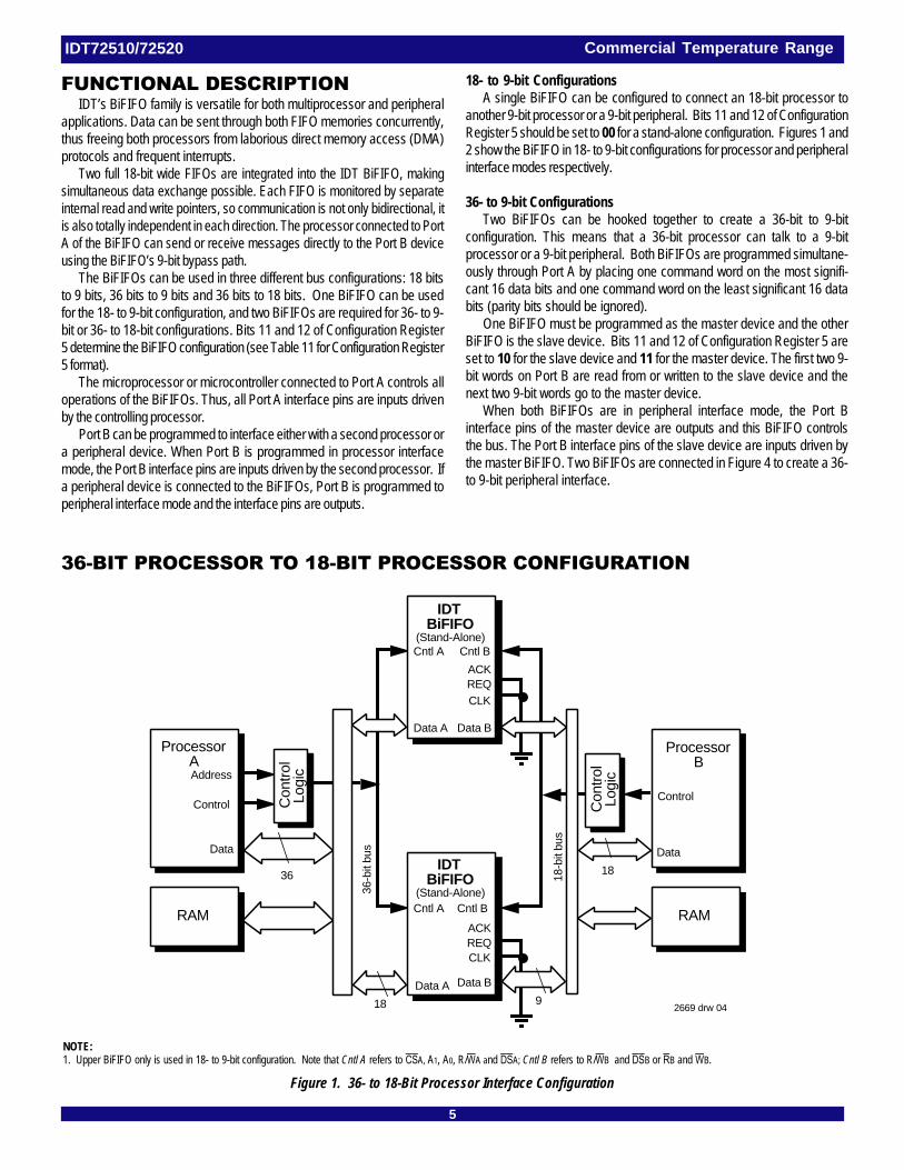
The BiFIFOs can be used in three different bus configurations: 18 bitsto 9 bits, 36 bits to 9 bits and 36 bits to 18 bits. One BiFIFO can be usedfor the 18- to 9-bit configuration, and two BiFIFOs are required for 36- to 9-bit or 36- to 18-bit configurations. Bits 11 and 12 of Configuration Register5 determine the BiFIFO configuration (see Table 11 for Configuration Register5 format).
The microprocessor or microcontroller connected to Port A controls alloperations of the BiFIFOs. Thus, all Port A interface pins are inputs drivenby the controlling processor.
Port B can be programmed to interface either with a second processor ora peripheral device. When Port B is programmed in processor interfacemode, the Port B interface pins are inputs driven by the second processor. Ifa peripheral device is connected to the BiFIFOs, Port B is programmed toperipheral interface mode and the interface pins are outputs.
18- to 9-bit ConfigurationsA single BiFIFO can be configured to connect an 18-bit processor to
another 9-bit processor or a 9-bit peripheral. Bits 11 and 12 of ConfigurationRegister 5 should be set to 00 for a stand-alone configuration. Figures 1 and2 show the BiFIFO in 18- to 9-bit configurations for processor and peripheralinterface modes respectively.
36- to 9-bit ConfigurationsTwo BiFIFOs can be hooked together to create a 36-bit to 9-bit
configuration. This means that a 36-bit processor can talk to a 9-bitprocessor or a 9-bit peripheral. Both BiFIFOs are programmed simultane-ously through Port A by placing one command word on the most signifi-cant 16 data bits and one command word on the least significant 16 databits (parity bits should be ignored).
One BiFIFO must be programmed as the master device and the otherBiFIFO is the slave device. Bits 11 and 12 of Configuration Register 5 areset to 10 for the slave device and 11 for the master device. The first two 9-bit words on Port B are read from or written to the slave device and thenext two 9-bit words go to the master device.
When both BiFIFOs are in peripheral interface mode, the Port Binterface pins of the master device are outputs and this BiFIFO controlsthe bus. The Port B interface pins of the slave device are inputs driven bythe master BiFIFO. Two BiFIFOs are connected in Figure 4 to create a 36-to 9-bit peripheral interface.
Figure 1. 36- to 18-Bit Processor Interface Configuration
NOTE:1. Upper BiFIFO only is used in 18- to 9-bit configuration. Note that Cntl A refers to CSA, A1, A0, R/WA and DSA; Cntl B refers to R/WB and DSB or RB and WB.
36-BIT PROCESSOR TO 18-BIT PROCESSOR CONFIGURATION
ProcessorA
Data
Address
Con
trol
Logi
c
RAM
Control
36
ProcessorB
Data
RAM
Con
trol
Logi
c
Control
18
2669 drw 04
IDTBiFIFO
(Stand-Alone)
Data A Data B
Cntl A Cntl B
ACK
IDTBiFIFO
(Stand-Alone)
Data A Data B
Cntl A Cntl B
18-b
it bu
s
36-b
it bu
s
18
REQ
ACKREQ
CLK
CLK
9
6
Commercial Temperature RangeIDT72510/72520
36-BIT PROCESSOR TO 18-BIT PERIPHERAL CONFIGURATION
NOTE:1. Upper BiFIFO only is used in 18- to 9-bit configuration. Note that Cntl A refers to CSA, A1, A0, R/WA and DSA; Cntl B refers to R/WB and DSB or RB and WB.
Figure 2. 36- to 18-Bit Peripheral Interface Configuration
assure fixed high states for RB and WB before they are programmed into anoutput, both pins should be pulled-up to VCC with 10K resistors.
If the BiFIFOs are in stand-alone configuration mode (18- to 9-bit, 36- to 18-bit, …), then the Port B interface pins are all outputs. Of course, only one setof Port B interface pins should be used to control a single peripheral device, whilethe other interface pins are all ignored. Figure 2 shows stand-alone configu-ration BiFIFOs connected to a peripheral.
In a 36- to 9-bit configuration, the master device controls the bus. The PortB interface pins of the master device are outputs and the interface pins of theslave device are inputs. A 36- to 9-bit configuration of two BiFIFOs connectedto a peripheral is shown in Figure 4.
Port A InterfaceThe BiFIFO is straightforward to use in microprocessor-based systems
because each BiFIFO port has a standard microprocessor control set. PortA has access to six resources: the A→B FIFO, the B→A FIFO, the 9-bitdirect data bus (bypass path), the configuration registers, status andcommand registers. The Port A Address and Read/Write pins determinethe resource being accessed as shown in Table 1. Data Strobe is used tomove data in and out of the BiFIFO.
When either of the internal FIFOs are accessed 18 bits of data aretransferred across Port A. Since the bypass path is only 9 bits wide, the leastsignificant byte with parity (DA0-DA7, DA16) is used on Port A. All of theregisters are 16 bits wide which means only the data bits (DA0-DA15) arepassed by Port A.
The two BiFIFOs shown in Figure 3 are configured to connect a 36-bitprocessor to a 9-bit processor.
36- to 18-bit ConfigurationsIn a 36- to 18-bit configuration, two BiFIFOs operate in parallel. Both
BiFIFOs are programmed simultaneously, 16 data bits to each device withthe 4 parity bits ignored.
Both BiFIFOs must be programmed into stand-alone mode for a 36-bitprocessor to communicate with an 18-bit processor or an 18-bit peripheral.This means that bits 11 and 12 of Configuration Register 5 must be set to00.
This configuration can be extended to wider bus widths (54- to 27-bits,72- to 36-bits, …) by adding more BiFIFOs to the configuration. Figures 1and 2 show multiple BiFIFOs configured for processor and peripheralinterface modes respectively.
Processor Interface ModeWhen a microprocessor or microcontroller is connected to Port B, all
BiFIFOs in the configuration must be programmed to processor interfacemode. In this mode, all Port B interface controls are inputs. Both REQ andCLK pins should be pulled LOW to ensure that the set-up and hold timerequirements for these pins are met during reset. Figures 1 and 3 showBiFIFOs in processor interface mode.
Peripheral Interface ModeIf Port B is connected to a peripheral controller, all BiFIFOs in the
configuration must be programmed in the peripheral interface mode. To
IDTBiFIFO
(Stand-Alone)
Processor PeripheralController
Data
Data A Data B
Data
Cntl A Cntl B
ACK
Address
ACK
Cntl
I/OData
IDTBiFIFO
(Stand-Alone)
Data A Data B
Cntl A Cntl B
Con
trol
Logi
c
RAM
18-b
it bu
s
36-b
it bu
s
18
REQ
REQ
ACKREQ
CLK
CLK
DMA or SystemClock
Control
18
9
36
2669 drw 05
7
Commercial Temperature RangeIDT72510/72520
36-BIT PROCESSOR TO 9-BIT PROCESSOR CONFIGURATION
NOTE:1. Cntl A refers to CSA, A1, A0, R/WA and DSA; Cntl B refers to R/WB and DSB or RB and WB.
Figure 3. 36- to 9-Bit Processor Interface Configuration
36-BIT PROCESSOR TO 9-BIT PERIPHERAL CONFIGURATION
NOTE:1. Cntl A refers to CSA, A1, A0, R/WA and DSA; Cntl B refers to R/WB and DSB or RB and WB.
Figure 4. 36- to 9-Bit Peripheral Interface Configuration
IDTBiFIFO(Master)
ProcessorA
ProcessorB
Data
Data A Data B
Data
Cntl A Cntl B
ACK
Address
IDTBiFIFO(Slave)
Data A Data B
Cntl A Cntl B
Contr
ol
Logic
RAM
9-b
it bus
36-b
it bus
18
REQ
ACKREQ
CLK
CLK
Control
RAM
Contr
ol
Logic
Control
2669 drw 06
IDTBiFIFO(Master)
Processor PeripheralController
Data
Data A Data B
Data
Cntl A Cntl B
ACK
Address
ACK
Cntl
I/OData
IDTBiFIFO(Slave)
Data A Data B
Cntl A Cntl B
Con
trol
Logi
c
RAM
9-bi
t bus
36-b
it bu
s
18
REQ
REQ
ACKREQ
CLK
CLK
DMA orSystemClock
Control
2669 drw 07
8
Commercial Temperature RangeIDT72510/72520
PORT A RESOURCES COMMAND OPERATIONS
2669 tbl 03
Table 1. Accessing Port A Resources Using CSA, A0, and A1
2669 tbl 04
Table 2. Functions Performed by Port A Commands
Bypass PathThe bypass path acts as a bidirectional bus transceiver directly between
Port A and Port B. The direct connection requires that the Port A interfacepins are inputs and the Port B interface pins are outputs. The bypass pathis 9 bits wide in an 18- to 9-bit configuration or in a 36- to 9-bit configuration.Only in the 36- to 18-bit configuration is the bypass path 18 bits wide.
During bypass operations, the BiFIFOs must be programmed into periph-eral interface mode. Bit 10 of Configuration Register 5 (see Table 11) is set to1 for peripheral interface mode. In a 36- to 9-bit configuration, both Port B databuses will be active. Data written into Port A will appear on both master andslave Port B buses concurrently. To avoid Port B bus contention, the data onDA0-DA7 and DA16 of both BiFIFOs should be exactly the same. Data read fromPort A will appear on pins DA0-DA7 and DA16 of both BiFIFOs within the same36-bit word.
Command RegisterTen registers are accessible through Port A, a Command Register, a
Status Register, and eight Configuration Registers.The Command Register is written by setting CSA = 0, A1 = 1, A0 = 1.
Commands written into the BiFIFO have a 4-bit opcode (bit 8 – bit 11) anda 3-bit operand (bit 0 – bit 2) as shown in Figure 5. The commands can beused to reset the BiFIFO, to select the Configuration Register, to performintelligent reread/rewrite, to set the Port B DMA direction, to set the StatusRegister format, to modify the Port B Read and Write Pointers, and to clearPort B parity errors. The command opcodes are shown in Table 2.
The reset command initializes different portions of the BiFIFO depend-ing on the command operand. Table 3 shows the reset command operands.
The Configuration Register address is set directly by the commandoperands shown in Table 4.
Intelligent reread/rewrite is performed by changing the Port B ReadPointer with the Reread Pointer or by changing the Port B Write Pointer withthe Rewrite Pointer. No command operands are required to perform areread/rewrite operation.
When Port B of the BiFIFO is in peripheral mode, the DMA direction iscontrolled by the Command Register. Table 5 shows the Port B read/writeDMA direction operands.
The BiFIFO supports two Status Register formats. Status Registerformat 1 gives all the internal flag status, while Status Register format 0provides the data in the Odd Byte Register. Table 6 gives the operands forselecting the appropriate Status Register format. See Table 8 for the detailsof the two Status Register formats.
Two commands are provided to increment the Port B Read and WritePointers in case reread/rewrite is performed. Incrementing the pointersguarantees that pointers will be on a word boundary when an odd numberof bytes is transmitted through Port B. No operands are required for thesecommands.
When parity check errors occur on Port B, a clear parity error commandis needed to remove the parity error. There are no operands for thesecommands.
ResetThe IDT72510 and IDT72520 have a hardware reset pin (RS) that resets
all BiFIFO functions. A hardware reset requires the following four condi-tions: RB and WB must be HIGH, RER and REW must be HIGH, LDRER andLDREW must be LOW, and DSA must be HIGH (Figure 9). After a hardwarereset, the BiFIFO is in the following state: Configuration Registers 0-3 are0000H, Configuration Register 4 is set to 6420H, and Configuration Regis-ters 5 and 7 are 0000H. Additionally, Status Register format 0 is selected,all the pointers including the Reread and Rewrite Pointers are set to 0, theodd byte register valid bit is cleared, the DMA direction is set to B→A write,the internal DMA request circuitry is cleared (set to its initial state), and allparity errors are cleared.
Figure 5. Format for Commands Written into Port A
COMMAND FORMAT15 12 11 8 7 3 2 0
X X X X Command Opcode X X X X X Command Operand2669 tbl 05
Table 6. Command Functions to Set the Status Register Format
2669 tbl 06
Table 3. Reset Command Functions
STATE AFTER RESET
2669 tbl 10
Table 7. The BiFIFO State After a Reset Command
2669 tbl 08
Table 5. Set DMA Direction Command Functions. Command Only Operates inPeripheral Interface Mode
A software reset command can reset A→B pointers and the B→Apointers to 0 independently or together. The request (REQ) DMA circuitrycan also be reset independently. A software Reset All command resets allthe pointers, the DMA request circuitry, and sets all the ConfigurationRegisters to their default condition. Note that a hardware reset is NOT thesame as a software Reset All command. Table 7 shows the BiFIFO stateafter the different hardware and software resets.
Status RegisterThe Status Register reports the state of the programmable flags, the
DMA read/write direction, the Odd Byte Register valid bit, and parity errors.The Status Register is read by setting CSA = 0, A1 = 1, A0 = 1 (see Table1).
There are two Status Register formats that are set by a Status Registerformat command. Format 0 stores the Odd Byte Register data in the lowereight bits of the Status Register, while format 1 reports the flag states andthe DMA read/write direction in the lower eight bits. The upper eight bits areidentical for both formats. The flag states, the parity errors, the Odd ByteRegister valid bit, and the Status Register format are all in the upper eightbits of the Status Register. See Table 8 for both Status Register formats.
Configuration RegistersThe eight Configuration Register formats are shown in Table 9. Configu-
ration Registers 0-3 contain the programmable flag offsets for the AlmostEmpty and Almost Full flags. These offsets are set to 0 when a hardwarereset or a software reset all is applied. Note that Table 9 shows thatConfiguration Registers 0-3 are 10 bits wide to accommodate the 1,024locations in each FIFO memory of the IDT72520. Only 9 least significantbits are used for the 512 locations of the IDT72510; the most significant bit,bit 9, must be set to 0.
Configuration Register 4 is used to assign the internal flags to theexternal flag pins (FLGA-FLGD). Each external flag pin is assigned aninternal flag based on the four bit codes shown in Table 10. The defaultcondition for Configuration Register 4 is 6420H as shown in Table 7. Thedefault flag assignments are: FLGD is assigned B→A Full, FLGC is as-signed B→A Empty, FLGB is assigned A→B Full, FLGA is assigned A→BEmpty.
Configuration Register 5 is a general control register. The format ofConfiguration Register 5 is shown in Table 11. Bit 0 sets the Intel-style
2669 tbl 11
interface (RB, WB) or Motorola-style interface (DSB, R/WB) for Port B. Bit 1changes the byte order for data coming through Port B. Bits 2 and 3 redefineFull and Empty Flags for reread/rewrite data protection.
Bits 4-9 control the DMA interface and are only applicable in peripheralinterface mode. In processor interface mode, these bits are don’t carestates. Bits 4 and 5 set the polarity of the DMA control pins REQ and ACK,respectively. An internal clock controls all DMA operations. This internalclock is derived from the external clock (CLK). Bit 9 determines the internalclock frequency: the internal clock = CLK or the internal clock = CLK dividedby 2. Bit 8 sets whether RB, WB, and DSB are asserted for either one or twointernal clocks. Bits 6 and 7 set the number of internal clocks between REQassertion and ACK assertion. The timing can be from 2 to 5 cycles as shownin Figure 17.
Bit 10 controls Port B processor or peripheral interface mode. Inprocessor mode, the Port B control pins (RB, WB, DSB, R/WB) are inputs andthe DMA controls are ignored. In peripheral mode, the Port B control pinsare outputs and the DMA controls are active.
Bits 11 and 12 set the width expansion mode. For 18- to 9-bitconfigurations or 36- to 18-bit configurations, the BiFIFO should be set instand-alone mode. For a 36- to 9-bit configuration, one BiFIFO must be inslave mode and the other BiFIFO must be in master mode. The masterBiFIFO allows the first two bytes transferred across Port B to go to the slaveBiFIFO, then the next two bytes go to the master BiFIFO.
Configuration Register 7 controls the parity functions of Port B as shownin Table 12. Either parity generation or parity checking is enabled for dataread and written through Port B. Bit 8 controls parity checking andgeneration for B→A write data. Bit 9 controls parity checking and genera-tion for A→B read data. Bit 10 controls whether the parity is odd or even.Bit 11 is used to assign the internal parity checking error to the FLGA pin.When the parity error is assigned to FLGA, the Configuration Register 4 flagassignment for FLGA is ignored.
STATUS REGISTER FORMAT 0 STATUS REGISTER FORMAT 1
Table 8. The Two Status Register Formats
2669 tbl 12
Bit Signal
0
1
2
3 Odd Byte Register
4
5
6
7
8 Valid Bit
9 Write Parity Error
10 Read Parity Error
11 Status Register Format = 0
12 A→B Full Flag
13 A→B Almost-Full Flag
14 B→A Empty Flag
15 B→A Almost-Empty Flag
Bit Signal
0 Reserved
1 Reserved
2 Reserved
3 DMA Direction
4 A→B Empty Flag
5 A→B Almost-Empty Flag
6 B→A Full Flag
7 B→A Almost-Full Flag
8 Valid Bit
9 Write Parity Error
10 Read Parity Error
11 Status Register Format = 1
12 A→B Full Flag
13 A→B Almost-Full Flag
14 B→A Empty Flag
15 B→A Almost-Empty Flag
11
Commercial Temperature RangeIDT72510/72520
CONFIGURATION REGISTER FORMATS
Programmable FlagsThe IDT BiFIFO has eight internal flags; four of these flags have program-
mable offsets, the other four are empty or full. Associated with each FIFO memoryarray are four internal flags, Empty, Almost-Empty, Almost-Full and Full, for thetotal of eight internal flags. The Almost-Empty and Almost-Full offsets can be setto any depth through the Configuration Registers 0-3 (see Table 9). The offset(or depth) of FIFO RAM array is based on the unit of an 18-bit word. The flagsare asserted at the depths shown in Table 13. After a hardware reset or asoftware reset all, the almost flag offsets are set to 0. Even though the offsets areequivalent, the Empty and Almost-Empty flags have different timing which meansthat the flags are not coincident. Similarly, the Full and Almost-Full flags are notcoincident because of timing.
These eight internal flags can be assigned to any of four external flag pins(FLGA-FLGD) through Configuration Register 4 (see Table 10). For the specificflag timings, see Figures 20-23.
The current state of all eight flags is available in the Status Register in StatusRegister format 1. In Status Register format 0, only four flags can be found inthe Status Register (see Table 8).
Port B InterfacePort B also has parity, reread/rewrite and DMA functions. Port B can be
configured to interface to either Intel-style (RB, WB) or Motorola-style (DSB, R/WB) devices in Configuration Register 5 (see Table 11). Port B can also beconfigured to talk to a processor or a peripheral device through ConfigurationRegister 5. In processor interface mode, the Port B interface controls are inputs.In peripheral interface mode, the Port B interface controls are outputs. After ahardware reset or a software Reset All command, Port B defaults to an Intel-style processor interface; the controls are inputs.
Two 9-bit words are put together to create each 18-bit word stored in theinternal FIFOs. The first 9-bit word written to Port B goes into the Odd Byte
EXTERNAL FLAG ASSIGNMENTCODES
2669 tbl 14
Table 10. Configuration Register 4 Internal Flag Assignments to External Flag Pins.
NOTE: 2669 tbl 13
1. Bit 9 of Configuration Registers 0-3 must be set to 0 on the IDT72510.
Table 9. The BiFIFO Configuration Register Formats
Assignment Code Internal Flag Assigned to Flag Pin
0000 A→B Empty
0001 A→B Almost-Empty
0010 A→B Full
0011 A→B Almost-Full
0100 B→A Empty
0101 B→A Almost-Empty
0110 B→A Full
0111 B→A Almost-Full
1000 A→B Empty
1001 A→B Almost-Empty
1010 A→B Full
1011 A→B Almost-Full
1100 B→A Empty
1101 B→A Almost-Empty
1110 B→A Full
1111 B→A Almost-Full
Config. Reg. 0
Config. Reg. 1
Config. Reg. 2
Config. Reg. 3
Config. Reg. 4
Config. Reg. 5
Config. Reg. 6
Config. Reg. 7
X
X
X
X
X
X
X
X
X
X
X
X
X
X
X
X
X
X
X
X
X
X
X
X
A→B FIFO Almost-Empty Flag Offset
A→B FIFO Almost-Full Flag Offset
B→A FIFO Almost-Empty Flag Offset
B→A FIFO Almost-Full Flag Offset
Flag D Pin Assignment Flag C Pin Assignment Flag B Pin Assignment Flag A Pin Assignment
General Control
Reserved
Parity Control
15
15
15
15
15
15
15
15
10
10
10
10
9
9
9
9
12 11 8 7 4 3
0
0
0
0
0
0
0
0
12
Commercial Temperature RangeIDT72510/72520
Register shown in the detailed block diagram. The Odd Byte Register valid bit(Bit 8) in the Status Register is 1 when this first 9-bit word is written. The databits from Port B (DB0-DB7) are also stored in the lower 8 bits of the Status Registerwhen Status Register format 0 is selected (see Table 8). The second write onPort B moves the 9-bits from Port B and the 9-bits in the Odd Byte Register intothe B→A FIFO and advances the B→A Write Pointer. The Status Register validbit is set to 0 after the second write.
When Port B reads data from the A→B FIFO, two buffers choose which9 of the 18 memory bits are sent to Port B. These buffers alternate betweenthe upper 9 bits (DA8-DA15, DA17) and the lower 9 bits (DA0-DA7, DA16). TheA→B Read Pointer is advanced after every two Port B reads.
The BiFIFO can be set to order the 9-bit data so the first 9-bits go to the LSB(DA0-DA7, DA16) or the MSB (DA8-DA15, DA17) of Port A. This data orderingis controlled by bit 1 of Configuration Register 5 (see Table 11).
DMA Control Interface The BiFIFO has DMA control to simplify data transfers with peripherals. For
the BiFIFO DMA controls (REQ, ACK and CLK) to operate, the BiFIFO mustbe in peripheral interface mode (Configuration Register 5, Table 11).
DMA timing is controlled by the external clock input, CLK. An internalclock is derived from this CLK signal to generate the RB, WB, DSB and R/WB output signals. The internal clock also determines the timing betweenREQ assertion and ACK assertion. Bit 9 of Configuration Register 5determines whether the internal clock is the same as CLK or whether theinternal clock is CLK divided by 2.
Bit 8 of Configuration Register 5 sets whether RB, WB and DSB are assertedfor 1 or 2 internal clocks. Bits 6 and 7 of Configuration Register 5 set the numberof clocks between REQ assertion and ACK assertion. The clocks between REQassertion and ACK assertion can be 2, 3, 4 or 5.
CONFIGURATION REGISTER 5 FORMAT
2669 tbl 15
Table 11. BiFIFO Configuration Register 5 Format
Bit Function
0 Select Port B Interface 0 Pins are RB and WB (Intel-style interface)
RB & WB or DSB & R/WB 1 Pins are DSB and R/WB (Motorola-style interface)
1 Byte Order of 18-bit Word 0 Lower byte DA7-DA0 and parity DA16 are read or written first on Port B
1 Upper byte DA15-DA8 and parity DA17 are read or written first on Port B
2 Full Flag Definition 0 Full Flag is asserted when write pointer meets read pointer
1 Full Flag is asserted when write pointer meets reread pointer
3 Empty Flag Definition 0 Empty Flag is asserted when read pointer meets write pointer
1 Empty Flag is asserted when read pointer meets rewrite pointer
4 REQ Pin Polarity 0 REQ pin active HIGH
1 REQ pin active LOW
5 ACK Pin Polarity 0 ACK pin active LOW
1 ACK pin active HIGH
00 2 internal clocks between REQ assertion and ACK assertion
7-6 REQ / ACK Timing 01 3 internal clocks between REQ assertion and ACK assertion
10 4 internal clocks between REQ assertion and ACK assertion
11 5 internal clocks between REQ assertion and ACK assertion
8 Port B Read and Write 0 RB, WB, and DSB are asserted for 1 internal clock
Timing Control for Peripheral Mode 1 RB, WB, and DSB are asserted for 2 internal clocks
9 Internal Clock 0 internal clock = CLK
Frequency Control 1 internal clock = CLK divided by 2
10 Port B Interface 0 Processor interface mode (Port B controls are inputs)
Mode Control 1 Peripheral interface mode (Port B controls are outputs)
00 Stand-alone mode (18- to 9-bits, 36- to 18-bits)
12-11 Width Expansion 01 Reserved
Mode Control 10 Slave width expansion mode (36- to 9-bits)
11 Master width expansion mode (36- to 9-bits)
13 Unused
14 Unused
15 Unused 2669 tbl 15
13
Commercial Temperature RangeIDT72510/72520
CONFIGURATION REGISTER 7 FORMAT
NOTE: 2669 tbl 17
1. BiFIFO flags can be assigned to external flag pins to be observed. D = FIFO depth (IDT72510 = 512, IDT72520 = 1,024), n = Almost-Empty flag offset, m = Almost-Full flag offset.
Table 13. Internal Flag Truth Table.
INTERNAL FLAG TRUTH TABLE
operation) for B->A operation; similarly, DA16 or parity bits from the RAM arraywill be passed to DB8 for A->B operations. A->B read parity errors and B->Awrite parity errors are shown in Bit 9 and 10 in the Status Register. If an externalparity error signal is required, a logical OR of the two parity error bits is broughtout to FLGA pin by setting Bit 11 of Configuration Register 7.
Parity generation creates the ninth bit. This ninth bit is placed on DB8 forA->B read operation, and on DA16 or RAM array for B->A write operation.
It is recommended that if the parity pins (DB8, DA16, and DA17) are notused, they should be pulled down with 10K resistors for noise immunity.
Intelligent Reread/RewriteIntelligent reread/rewrite is a method the BiFIFO uses to help assure data
integrity. Port B of the BiFIFO has two extra pointers, the Reread Pointer andthe Rewrite Pointer. The Reread Pointer is associated with the A->B FIFO ReadPointer, while the Rewrite Pointer is associated with the B->A FIFO Write Pointer.The Reread Pointer holds the start address of a data block in the A->B FIFORAM, and the Read Pointer is the current address of the same FIFO RAM array.By loading the Read Pointer with the value held in the Reread Pointer (RERasserted), reads will start over at the beginning of the data block. In order to markthe beginning of a data block, the Reread Pointer should be loaded with the ReadPointer value (LDRER asserted) before the first read is performed on this datablock. Figure 6 shows a Reread operation.
Bits 4 and 5 of Configuration Register 5 set the polarity of the REQ and ACKpins, respectively.
A DMA transfer command sets the Port B read/write direction (see Table5). The timing diagram for DMA transfers is shown in Figure 17. The basicDMA transfer starts with REQ assertion. After 2 to 5 internal clocks, ACKis asserted by the BiFIFO. ACK will not be asserted if a read is attemptedon an Empty A→B FIFO or if a write is attempted on a Full B→A FIFO. Ifthe BiFIFO is in Motorola-style interface mode, R/WB is set at the same timethat ACK is asserted. One internal clock later, DSB is asserted. If the BiFIFOis in Intel-style interface mode, either RB or WB is asserted one internal clockafter ACK assertion. These read/write controls stay asserted for 1 or 2internal clocks, then ACK, DSB, RB and WB are made inactive. Thiscompletes the transfer of one 9-bit word.
On the next rising edge of CLK, REQ is sampled. If REQ is still asserted,another DMA transfer starts with the assertion of ACK. Data transfers willcontinue as long as REQ is asserted.
Parity Checking and GenerationParity generation or checking is performed by the BiFIFO on data
passing through Port B. Parity can either be odd or even as determined byBit 10 of Configuration Register 7.
When parity checking is enabled, DB8 is treated as a data bit. DB8 data willbe passed to DA16 (bypass operation) or stored in the RAM array (FIFO
11 Assign Parity Error to 0 No Parity Error Output
Flag A Pin 1 Parity Error on Flag A Pin
12-15 Unused
Number of Words in FIFO
From To Empty Flag Almost-Empty Flag Almost-Full Flag Full Flag
0 0 Asserted Asserted Not Asserted Not Asserted
1 n Not Asserted Asserted Not Asserted Not Asserted
n + 1 D - (m + 1) Not Asserted Not Asserted Not Asserted Not Asserted
D - m D - 1 Not Asserted Not Asserted Asserted Not Asserted
D D Not Asserted Not Asserted Asserted Asserted
14
Commercial Temperature RangeIDT72510/72520
Similarly, the Rewrite Pointer holds the start address of a data block in theB->A FIFO RAM, while the Write Pointer is the current address within the RAMarray. The operation of the REW and LDREW is identical to the RER and LDRERdiscussed above. Figure 7 shows a Rewrite operation.
For the reread data protection, Bit 2 of Configuration Register 5 can be setto 1 to prevent the data block form being overwritten. In this way, the assertionof A->B full flag will occur when the write pointer meets the reread pointer insteadof the read pointer as in the normal definition. For the rewrite data protection,
REWRITE OPERATIONS (1,2)REREAD OPERATIONS (1,2)
NOTES:1. If bit 3 is set to 1,
Empty flag asserted if Read = RewriteFull flag asserted if Read + FIFO size = Write
2. If bit 3 is set to 0,Empty flag asserted if Read = WriteFull flag asserted if Read + FIFO size = Write
Figure 7. BiFIFO Rewrite Operations
NOTES:1. If bit 2 is set to 1,
Empty flag asserted if Read = WriteFull flag asserted if Reread + FIFO size = Write
2. If bit 2 is set to 0,Empty flag asserted if Read = WriteFull flag asserted if Read + FIFO size = Write
Figure 6. BiFIFO Reread Operations
WritePointer
RereadPointer
ReadPointer
A→BFIFO
Rereadfunction
LoadRereadfunction
2669 drw 08
Bit 3 of Configuration Register 5 can be set to 1 to prevent the data block frombeing read. In this case, the assertion of B->A empty flag will occur when theread pointer meets the rewrite pointer instead of the write pointer.
In conclusion, Bit 2 and 3 of Configuration Register 5 are used to redefineFull & Empty flags for data block partition. Although it can serve the purpose ofdata protection, the setting of these 2 bits is independent of the functions causedby RER/REW, or LDRER/LDREW assertions.
WritePointer
ReadPointer
RewritePointer
B→AFIFO
Rewritefunction
Load Rewritefunction
2669 drw 09
15
Commercial Temperature RangeIDT72510/72520
ABSOLUTE MAXIMUM RATINGS(1)
Symbol Rating Commercial UnitVTERM Terminal Voltage –0.5 to +7.0 V
with Respect to Ground
TSTG Storage Temperature –55 to +125 °C
IOUT DC Output Current –50 to +50 mA
NOTE: 2669 tbl 18
1. Stresses greater than those listed under ABSOLUTE MAXIMUM RATINGS may causepermanent damage to the device. This is a stress rating only and functional operation ofthe device at these or any other conditions above those indicated in the operationalsections of this specification is not implied. Exposure to absolute maximum ratingconditions for extended periods may affect reliabilty.
CAPACITANCE (TA = +25°C, f = 1.0MHz)
NOTES: 2669 tbl 22
1. With output deselected.2. Characterized values, not currently tested.
RECOMMENDED DCOPERATING CONDITIONS
Symbol Parameter Min. Typ. Max. Unit
VCC Supply Voltage 4.5 5.0 5.5 V
GND Supply Voltage 0 0 0 V
VIH Input HIGH Voltage 2.0 — — V
VIL(1) Input LOW Voltage — — 0.8 V
TA Operating Temperature 0 — 70 °CCommercial
NOTE: 2669 tbl 19
1. 1.5V undershoots are allowed for 10ns once per cycle.
Figure 8. Output Load* Includes jig and scope capacitances
AC TEST CONDITIONS
2669 tbl 21
DC ELECTRICAL CHARACTERISTICS(Commercial: Vcc = 5V ± 10%, TA = 0°C to +70°C)
IDT72510LIDT72520L
CommercialtCLK = 25, 35, 50 ns
Symbol Parameter Min. Typ. Max. Unit
ILI(1) Input Leakage Current (any input) –1 — 1 µA
ILO(2) Output Leakage Current –10 — 10 µA
VOH Output Logic “1” Voltage, IOUT = –1 mA 2.4 — — V
VOL Output Logic “0” Voltage, IOUT = 4 mA — — 0.4 V
2669 tbl 23NOTES:1. The minimum data hold time is 5ns (10ns for the 80ns speed grade) when writing to the Commnad of Configuration registers.
17
Commercial Temperature RangeIDT72510/72520
AC ELECTRICAL CHARACTERISTICS(Commercial: VCC = 5V±10%, TA = 0°C to +70°C)
Commercial
IDT72510L25 IDT72510L35 IDT72510L50
IDT72520L25 IDT72520L35 IDT72520L50 Timing
Symbol Parameter Min. Max. Min. Max. Min. Max. Unit Figure
PORT B PROCESSOR INTERFACE TIMING
tbA1 Port B access time with noparity
— 25 — 35 — 50 ns 13, 14, 15
tbA2 Port B access time with parity — 30 — 42 — 60 ns 13, 14, 15
tbLZ Read or write pulse LOW todata bus at Low-Z
5 — 5 — 5 — ns 13, 14, 15
tbHZ Read or write pulse HIGH todata bus at High-Z
— 15 — 20 — 30 ns 13, 14, 15
tbDV Data valid from read pulseHIGH
5 — 5 — 5 — ns 13, 14, 15, 16
tbRC Read cycle time 35 — 45 — 65 — ns 13
tbRPW Read pulse width 25 — 35 — 50 — ns 13
tbRR Read recovery time 10 — 10 — 15 — ns 13
tbS R/WB set-up time 5 — 5 — 5 — ns 13
tbH R/WB hold time 5 — 5 — 5 — ns 13
tbDS1 Data set-up time with no parity 15 — 18 — 30 — ns 13, 14, 15
tbDH1 Data hold time with no parity 0 — 0 — 5 — ns 13, 14, 15
tbDS2 Data set-up time with parity 18 — 22 — 35 — ns 13, 14, 15
tbDH2 Data hold time with parity 0 — 0 — 5 — ns 13, 14, 15
tbWC Write cycle time 35 — 45 — 65 — ns 13
tbWPW Write pulse width 25 — 35 — 50 — ns 13, 15
tbWR Write recovery time 10 — 10 — 15 — ns 13
PORT B PERIPHERAL INTERFACE TIMING
tbA1 Port B access time with noparity
— 25 — 40 — 55 ns 17
tbA2 Port B access time with parity — 30 — 42 — 60 ns 17
tbCKC Clock cycle time 15 — 20 — 25 — ns 17
tbCKH Clock pulse HIGH time 6 — 6 — 10 — ns 17
tbCKL Clock pulse LOW time 6 — 6 — 10 — ns 17
tbREQS Request set-up time 5 — 5 — 10 — ns 17
tbREQH Request hold time 5 — 5 — 5 — ns 17
tbACKL Delay from a rising clock edgeto ACK switching
— 15 — 18 — 25 ns 17
2669 tbl 24
18
Commercial Temperature RangeIDT72510/72520
NOTES: 2669 tbl 25
1. Read and Write are internal signals derived from DSA, R/WA, DSB, R/WB, RB and WB.2. Although the flags, Empty, Almost-Empty, Almost-Full and Full Flags are internal flags , the timing given is for those assigned to external pins.3. Values guaranteed by design, not currently tested.
AC ELECTRICAL CHARACTERISTICS(Commercial: VCC = 5V±10%, TA = 0°C to +70°C)
Commercial
IDT72510L25 IDT72510L35 IDT72510L50
IDT72520L25 IDT72520L35 IDT72520L50 Timing
Symbol Parameter Min. Max. Min. Max. Min. Max. Unit Figure
PORT B RETRANSMIT and PARITY TIMING
tbDSBH RER, REW, LDRER, LDREWset-up and recovery time
10 — 10 — 15 — ns 9, 18
tbPER Parity error time 20 — 25 — 30 — ns 19
BYPASS TIMING
tBYA Bypass access time — 15 — 20 — 30 ns 16
tBYD Bypass delay — 10 — 15 — 20 ns 16
taBYDV Bypass data valid time fromDSA
15 — 15 — 15 — ns 16
tbBYDV (3) Bypass data valid time fromDSB
3 — 3 — 3 — ns 16
FLAG TIMING
tREF Read clock edge to EmptyFlag asserted
— 25 — 35 — 45 ns 14, 15, 20, 22
tWEF Write clock edge to EmptyFlag not asserted
— 25 — 35 — 45 ns 14, 15, 20, 22
tRFF Read clock edge to Full Flagnot asserted
— 25 — 35 — 45 ns 14, 15, 21, 23
tWFF Write clock edge to Full Flagasserted
— 25 — 35 — 45 ns 14, 15, 21, 23
tRAEF Read clock edge to Almost-Empty Flag asserted
— 40 — 50 — 60 ns 20, 22
tWAEF Write clock edge to Almost-Empty Flag not asserted
— 40 — 50 — 60 ns 20, 22
tRAFF Read clock edge to Almost-Full Flag not asserted
— 40 — 50 — 60 ns 21, 23
tWAFF Write clock edge to Almost-Full Flag asserted
— 40 — 50 — 60 ns 21, 23
19
Commercial Temperature RangeIDT72510/72520
Figure 10. Basic Port A Control Signal Timing (Applies to All Port A Timing)
Figure 11. Port A Command Timing (Write)
Figure 9. Hardware Reset Timing
tRStRSC
tRSS
RS
WB, RB(or R/WB, DS )
,REW
LDRERLDREW
REQ
DSA
FLGA,FLGC
tRSR
tRSF
FLGB,
FLGD
B
RER
2669 drw 11
tRSR
tRSF
taS
CSA
A0, A1
R/WA
DSA
taH
2669 drw 12
taDS
R/WA
DSA
OpcodeDA8-DA12
or
taDH
tWPW
2669 drw 13
tWRCOM
DA0-DA2Operand
20
Commercial Temperature RangeIDT72510/72520
tbDS1 or tbDS2
(R/WB)
WB
(or DSB)
InputDB0-DB8
tbDH1 or tbDH2
tbS
tbWC
tbWPW tbWR tbH
RB
(or DSB)
OutputDB0-DB8
tbS
tbLZ tbA1 or tbA2 tbHZ
tbDV
tbRPW tbRR tbHtbRC
(R/WB)
2669 drw 15
WRITE
NOTES:1. tbA1 is with parity checking or if parity is ignored, tbA2 is with parity generation.2. RB = 1
Figure 13. Port B Read and Write Timing, Processor Interface Mode Only
WRITE
NOTES:1. tbDS1 and tbDH1 are with parity checking or if parity is ignored, tbDS2 and tbDH2 are with parity generation.2. RB = 1
READ
READ
Figure 12. Read and Write Timing for Port A
InputDA0 - DA17
OutputDA0 - DA17
taDS
R/WA
DSA
taDH
taS
taWC
taWPW taWR taH
R/WA
DSA
taS
taLZtaA taHZ
taDV
taRPW taRR taHtaRC
2669 drw 14
21
Commercial Temperature RangeIDT72510/72520
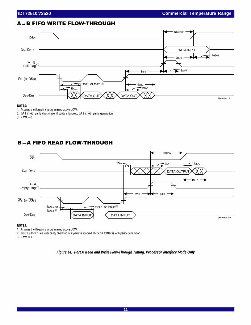
A→→→→→B FIFO WRITE FLOW-THROUGH
NOTES:1. Assume the flag pin is programmed active LOW.2. tbA1 is with parity checking or if parity is ignored, tbA2 is with parity generation.3. R/WA = 0
B→→→→→A FIFO READ FLOW-THROUGH
NOTES:1. Assume the flag pin is programmed active LOW.2. tbDS1 & tbDH1 are with parity checking or if parity is ignored, tbDS2 & tbDH2 is with parity generation.3. R/WA = 1
Figure 14. Port A Read and Write Flow-Through Timing, Processor Interface Mode Only
DATA OUTPUT
DSA
DA0-DA17
WB (or DSB)
B→AEmpty Flag
DB0-DB8
taDVtaA
DATA INPUTDATA INPUT
taRPW
taLZ
taHZ
tREFtWEF
tbDS1 ortbDS2
tbDH1 or tbDH2
2669 drw 16a
(1)
(2)
(2)
DATA OUT
DATA INPUT
DATA OUT
DSA
DA0-DA17
taWPW
taDStaDH
tWFFtRFF
tbDVtbHZ
tbLZ
tbA1 or tbA2
RB (or DSB)
DB0-DB82669 drw 16
A→B(1)Full Flag
(2)
22
Commercial Temperature RangeIDT72510/72520
DATA OUT
DSA
DA0-DA17
tbDS1 or tbDS2
tRFF tWFF
taHZtaA
WB (or DSB)
DB0-DB8 DATA INPUT
taLZ
tbWPW
(1)
taDS taDH
DATA INPUT
tWEF tREF
DATA OUT
tbHZtbA1 or tbA2tbLZ tbDV
tbRPW
DATA OUT
DSA
DA0-DA17
RB (or DSB)
A→BEmpty Flag
DB0-DB8
2669 drw 17
B→AFull Flag
tbDH1 or tbDH2 (2)
(1)
(2)
B→→→→→A FIFO WRITE FLOW-THROUGH
NOTES:1. Assume the flag pin is programmed active LOW.2. tbDS1 & tbDH1 are with parity checking or if parity is ignored, tbDS2 & tbDH2 are with parity generation.3. R/WA = 1
NOTES:1. Assume the flag pin is programmed active LOW.2. tbA1 is with parity checking or if parity is ignored, tbA2 is with parity generation.3. R/WA = 0
Figure 15. Port B Read and Write Flow-Through Timing
A→→→→→B FIFO READ FLOW-THROUGH
23
Commercial Temperature RangeIDT72510/72520
RB (or DSB)(2)
BYTE 2
BYTE 0 BYTE 1
BYTE 1
taS
BYTE 0
R/WA
DSA
DA0-DA7,
DA16
taS
taLZ taDV
tBYA
BYTE 1
taH
taHZ
tBYD tBYD
tBYD tBYD
BYTE 0 BYTE 1 BYTE 2
tBYD
(R/WB)
DB0-DB8
taH
tbLZ taBYDVtBYA
BYTE 2
tbHZ
BYTE 0 BYTE 2
tBYD
tBYD
tBYDtBYDtBYD
R/WA
DSA
DA0-DA7,
DA16
(R/WB)
DB0-DB8
(1)
(1)
(1)
(1)
tbBYDV
WB (or DSB)(2)
2669 drw 18
B→→→→→A READ BYPASS
A→→→→→B WRITE BYPASS
NOTES:1. Once the bypass starts, any data changes on Port A bus (Byte 0→ Byte 1) will be passed to Port B bus.2. RB = 1.
Figure 16. Bypass Path Timing. BiFIFO Must be in Peripheral Interface Mode.
NOTES:1. Once the bypass starts, any data changes on Port B bus (Byte 0→ Byte 1) will be passed to Port A bus.2. WB = 1.
24
Commercial Temperature RangeIDT72510/72520
CLK
tREQS
REQ
ACK
(R/WB)
tbHZ
tbLZ tbDV
tREQH
tCKH tCKLtCKC
2 to 5 cycles 1 cycle1 to 2 cycles
tACKL
WRITE
READtbA1 or tbA2
tACKL tACKL
tbDH1 or tbDH2
2 to 5cycles
1 to 2cycles 2 to 5
cycles
1 to 2cycles
CLK
REQ
WB (or DSB)
OutputDB0-DB17
(R/WB)
RB (or DSB)
InputDB0-DB17
ACK, R/WB
RB, WB (or DSB)
tbDS1 or tbDS2
tACKL
tACKL
2669 drw 19
BLOCK DMA TRANSFER
SINGLE WORD DMA TRANSFER
NOTES:1. tbA1, tbDS1and tbDH1are with parity checking or if parity is ignored, tbA2 & tbDS2 and tbDH2 are with parity.
Figure 17. Port B Read and Write DMA Timing, Peripheral Interface Mode Only
25
Commercial Temperature RangeIDT72510/72520
R/WB
RB, WB (or DSB)
FLGA
tbS
tPER
R/WA
DSA
FLGA
taS
tPER
2669 drw 21
tbH
taH
NOTE:1. FLGA is the only pin that can be assigned as a parity error output.
Figure 19. Port B Parity Error Timing
Figure 18. Port B Reread and Rewrite Timing for Intelligent Retransmit
SET PARITY ERROR: FLGA IS ASSIGNEDAS THE PARITY ERROR PIN
CLEAR PARITY ERROR: COMMANDWRITTEN INTO PORT A CLEARSPARITY ERROR ON FLGA PIN
RB, WB
(or R/WB, DSB)
RER,REW
tbDSBH
LDRER,LDREW
tbDSBH tbWPWH
2669 drw 20
26
Commercial Temperature RangeIDT72510/72520
Figure 20. Empty and Almost-Empty Flag Timing for B→→→→→ A FIFO. (n = Programmed Offset)
NOTES:1. B→ A FIFO initially contains D–(M+1) data words. D = 512 for IDT 72510; D = 1,024 for IDT72520.2. Assume the flag pins are programmed active LOW.3. For stand-alone mode only; in a 36- to 9-bit configuration, Port B reads must be doubled.4. R/WA = 1
Figure 21. Full and Almost-Full Flag Timing for B→→→→→ A FIFO. (m = Programmed Offset)
NOTES:1. A→ B FIFO is initially empty.2. Assume the flag pins are programmed active LOW.3. For stand-alone mode only; in a 36- to 9-bit configuration, Port B reads must be doubled.4. R/WA = 1
Figure 22. Empty and Almost-Empty Flag Timing for A→→→→→ B FIFO. (n = Programmed Offset)
DSA
tRAEF
tWEF
WB
(or R/WB=0,DSB)
B→AEmpty Flag
B→A Almost-Empty Flag
Read
1 2 n+1
Write 2n+1
1 2 3 4
2n+2
tREF
tWAEF
2669 drw 22
DSA
tWAFF
WB
(or R/WB=0,DSB)
B→A Almost-Full Flag
B→AFull Flag
Read
1 2 m+1
Write 2m+1
1 2 3 4
2m+2
tWFF tRFF
tRAFF
2669 drw 23
A→BAlmost-Empty Flag
DSA
Write
1 2 n+1
tRAEF
tWEF
RB
(or R/WB=1, DS B)
A→BEmpty Flag
Read 2n+1
1 2 3 4
2n+2
tREF
tWAEF
2669 drw 24
NOTES:1. B→ A FIFO is initially empty.2. Assume the flag pins are programmed active LOW.3. For stand-alone mode only; in a 36- to 9-bit configuration, Port B reads must be doubled.4. R/WA = 1
27
CORPORATE HEADQUARTERS for SALES: for TECH SUPPORT:2975 Stender Way 800-345-7015 or 408-727-6116 408-330-1753Santa Clara, CA 95054 fax: 408-492-8674 [email protected]
www.idt.com
ORDERING INFORMATION
NOTES:1. A→ B FIFO initially contains D–(M+1) data words. D = 512 for IDT 72510; D = 1,024 for IDT72520.2. Assume the flag pins are programmed active LOW.3. For stand-alone mode only; in a 36- to 9-bit configuration, Port B reads must be doubled.4. R/WA = 0
NOTE:1. Industrial temperature range is available by special order.
Figure 23. Full and Almost-Full Flag Timing for A→→→→→ B FIFO. (m = Programmed Offset)
DSA
Write
1 2 m+1
tWFF
tWAFF
B→AAlmost- Full Flag
B→A FullFlag
Read 2m+1
1 2 3 4
2m+2
tRFF
tRAFF
RB(or R/WB=1, DSB)
2669 drw 25
L
Power
XX
Speed
J
Package Process/Temperature
Range
Blank
253550
L
XXXXX
Device Type
7251072520
IDT
2669 drw 26
J
Commercial (0°C to +70°C)
Low Power
512 x 18 or 1,024 x 9 BiFIFO1,024 x 18 or 2,048 x 9 BiFIFO


![ABSOLUTE RESPONSE - Panasonic · ABSOLUTE RESPONSE Specifications ... 1,824 x 1,024* [1:1] 3,456 x 3,456 (L), 2,448 x 2,448 (M), 1,744 x 1,744 (S), 1,712 x 1,712* ... NFC ISO/IEC](https://static.documents.pub/doc/80x56/5ac638207f8b9a57528e160b/absolute-response-response-specifications-1824-x-1024-11-3456-x-3456.jpg)


