Chip Design • www.chipdesignmag.com December / January 2006 • 21 Foundry Support ANALOG By Albert Yen Foundry Support Is Critical to SoC Design and Implementation By closely coupling analog/RF design and foundry support, designers gain greater assurance of successful system-on-a-chip integration. D esigners tasked with creating the analog/radio-frequency (RF) portion of system-on-a-chip (SoC) products face a considerable array of challenges. For example, different design considerations and architectures are required by system specifications within varying operating frequencies, transmission methods, digital modulations, signal-to-noise ratios, and data rates. ese varying specifications create further complications when coupled with the range of RF design requirements pertaining to time and frequency domain, system verification, parasitics, and packaging. Foundry architectures and sophisticated design methodologies are available to address complex mixed-mode systems. To handle new and emerging challenges, however, they must undergo constant innovation. Such innovation will guarantee that purely analog and RF components come to market faster and in the same process generations as their digital IC counterparts. One such innovation is the close coupling of analog/RF design and foundry support. By closely tying together these traditionally discrete efforts, designers can be more readily assured of successful SoC integration. To better understand the significance of a closely coupled relationship between the analog/RF design process and foundry support, one must be aware of the challenges facing today’s analog and RF designers. Many of these challenges stem from the global consumer marketplace’s increasing demand for ever-smaller, ever-more-feature-rich wireless products. Plus, analog/RF design--by its very nature--is an extremely complex and difficult task. ese combined factors result in a range of new RF design requirements with which designers must now contend. ese requirements include: • Time and frequency domain System architects typically develop algorithms in the time domain--a process that is conducive to creating signal-flow algorithms. In contrast, RF engineers usually work in the frequency domain. ey deal with the frequency responses of amplifiers, filters, mixers, and so forth in terms of network parameters as well as frequency-dependent noise and nonlinearity. In addition, RF engineers specify hardware and design circuits and run simulations using frequency-domain simulators. ey also perform physical tests and generate mountains of data. Unfortunately, the output of these powerful, circuit-level simulators is incompatible with the baseband- complex, time-domain-modeling methods used by system architects. Network-analyzer measurements provide another source of network parameter data. In its frequency-domain format, however, the integration of this data into a time-domain system model for verification is challenging at best. • System-verification coverage System verification poses another challenge for the analog and RF designer--especially given the accuracy, capacity, and speed required for sensitive analog simulation. Achieving an acceptable level of coverage also is troublesome, as the simulation of a full transceiver chain often exceeds the limits of traditional electronic-design-automation (EDA) tools. Due to the long simulation run time and short design schedules, the analog and RF designer is often forced to compromise on the breadth of verification simulations. • Parasitics and packaging With their active and passive devices, analog and RF circuits are complex and extremely sensitive. As a result, early estimates of RF parasitics (e.g., mutual inductance coupling, distributed layout parasitics, substrate coupling effects, inter-stage impedances, and power-supply noise) can be quite daunting--especially given the potential for multiple RF cores to be integrated on the same die. In addition, designers must face the added challenges associated with the integration of the analog/RF and digital domains in an SoC. Examples of such challenges include on-chip passives (e.g., spiral inductors) and substrate crosstalk. Consider, for example, that a low-noise amplifier (LNA) may employ multiple integrated inductors. e magnetic coupling between them and other inductors on chip (e.g., multiple voltage-controlled- oscillator [VCO] tanks) can seriously affect system performance. It may even lead to design failure. Parasitic problems also exasperate designers at the package level. In fact, the electrical parasitics arising from the packaged product have become a key problem for chip designers. is issue has brought packaging into the spotlight as a system-level concern.
Transcript
Chip Design • www.chipdesignmag.com December / January 2006 • 21
Foundry Supportan
alog
By albert Yen
Foundry Support Is Critical to SoC Design and Implementation
By closely coupling analog/RF design and foundry support, designers gain greater assurance of successful system-on-a-chip integration.
Designers tasked with creating the analog/radio-frequency (RF) portion of system-on-a-chip (SoC) products
face a considerable array of challenges. For example, different design considerations and architectures are required by system specifications within varying operating frequencies, transmission methods, digital modulations, signal-to-noise ratios, and data rates. These varying specifications create further complications when coupled with the range of RF design requirements pertaining to time and frequency domain, system verification, parasitics, and packaging. Foundry architectures and sophisticated design methodologies are available to address complex mixed-mode systems. To handle new and emerging challenges, however, they must undergo constant innovation. Such innovation will guarantee that purely analog and RF components come to market faster and in the same process generations as their digital IC counterparts. One such innovation is the close coupling of analog/RF design and foundry support. By closely tying together these traditionally discrete efforts, designers can be more readily assured of successful SoC integration.
To better understand the significance of a closely coupled relationship between the analog/RF design process and foundry support, one must be aware of the challenges facing today’s analog and RF designers. Many of these challenges stem from the global consumer marketplace’s increasing demand for ever-smaller, ever-more-feature-rich wireless products. Plus, analog/RF design--by its very nature--is an extremely complex and difficult task. These combined factors result in a range of new RF design requirements with which designers must now contend. These requirements include:
• Time and frequency domain
System architects typically develop algorithms in the time domain--a process that is conducive to creating signal-flow algorithms. In contrast, RF engineers usually work in the frequency domain. They deal with the frequency responses of amplifiers, filters, mixers, and so forth in terms of network parameters as well as frequency-dependent noise and nonlinearity. In addition, RF engineers specify hardware and design circuits and run simulations using frequency-domain simulators. They also perform physical tests and generate
mountains of data. Unfortunately, the output of these powerful, circuit-level simulators is incompatible with the baseband-complex, time-domain-modeling methods used by system architects. Network-analyzer measurements provide another source of network parameter data. In its frequency-domain format, however, the integration of this data into a time-domain system model for verification is challenging at best.
• System-verification coverage
System verification poses another challenge for the analog and RF designer--especially given the accuracy, capacity, and speed required for sensitive analog simulation. Achieving an acceptable level of coverage also is troublesome, as the simulation of a full transceiver chain often exceeds the limits of traditional electronic-design-automation (EDA) tools. Due to the long simulation run time and short design schedules, the analog and RF designer is often forced to compromise on the breadth of verification simulations.
• Parasitics and packaging
With their active and passive devices, analog and RF circuits are complex and extremely sensitive. As a result, early estimates of RF parasitics (e.g., mutual inductance coupling, distributed layout parasitics, substrate coupling effects, inter-stage impedances, and power-supply noise) can be quite daunting--especially given the potential for multiple RF cores to be integrated on the same die. In addition, designers must face the added challenges associated with the integration of the analog/RF and digital domains in an SoC. Examples of such challenges include on-chip passives (e.g., spiral inductors) and substrate crosstalk. Consider, for example, that a low-noise amplifier (LNA) may employ multiple integrated inductors. The magnetic coupling between them and other inductors on chip (e.g., multiple voltage-controlled-oscillator [VCO] tanks) can seriously affect system performance. It may even lead to design failure.
Parasitic problems also exasperate designers at the package level. In fact, the electrical parasitics arising from the packaged product have become a key problem for chip designers. This issue has brought packaging into the spotlight as a system-level concern.
22 • December / January 2006 Chip Design • www.chipdesignmag.com
Foun
dry
Supp
ort
anal
og
By albert Yen
When they’re coupled with varying system specifications, these RF requirements make the challenge faced by today’s analog and RF designers even more difficult. The degree of difficulty will vary for different systems. Consider, for example, a successful RF CMOS SoC product that integrates Bluetooth and IEEE 802.11b, such as UltimateBlue SiW3500 from SiliconWave, MCM2033B1 from Broadcom, or BC212015 from Cambridge Silicon Radio. Because these products have lower data-rate requirements, they’re easier to implement as RF CMOS ICs. Yet other, more stringent system requirements would require more integrated SoCs.
DealIng WIth ChallengeSTo cope with these new challenges and RF requirements, the designers creating the analog/RF portion of SoC designs need considerable additional support from the foundry. To better illustrate the depth of this need, consider the example of a simple component: an inductor. A design kit can be used to help generate a design’s layout and an electrical model. In this example, suppose that a set of spiral-inductor libraries and high-frequency passive components are built into the design kit. Examples of such components include metal-insulator-metal or metal-oxide-metal capacitors. While the kit is a big help to the designer, input from the foundries is still needed for successful analog-design tapeout.
The problem, of course, is that most foundries currently provide only corner-case device models for device modeling. While these models may be good enough for digital design, they’re often not well suited for analog/RF designs. Ideally, a model library should include the following: corner cases, statistical models, digital/analog mismatch models, pad models with RF electrostatic discharge, flicker-noise models, and substrate-resistance models. The library also should include well-proximity and shallow-trench isolation stress effects.
For many years, some foundries just provided a set of spiral-inductor libraries. Other foundries only provided libraries of square ones. Because these libraries didn’t provide a full and complete offering of models, it was easy to miss considerations like the interference between different inductors. Instead, the spiral inductor was viewed as a discrete component. Effects like interference simply weren’t considered. The performance of the design was therefore degraded. Spiral inductors are used throughout RF ICs. Yet the design engineer would rarely adopt the inductor from a foundry design kit.
UMC is an example of one foundry that provides hexagonal, circular, and square inductors for its various processes. Some designers opt to use a hexagonal spiral, however, while others
prefer a circular spiral. Still others may prefer a square spiral or even a single-end spiral. For the foundry, trying to satisfy all customer requests by providing various sizes, shapes, and symmetrical/single-end spirals is often an endless and futile effort (see Figure 1).
For a design house to create a spiral inductor for different designs, the engineer usually needs to model the process layer in order
to accommodate an electromagnetic (EM) simulator. Examples include HFSS from Ansoft or ASITIC from the University of California at Berkeley. Next, a silicon test structure is fabricated and measured. A model is then created for simulation. The entire process is often reiterated several times. Because this process is very time-consuming, it often eats up a huge part of the development cycle. As a result, it can be extremely expensive. This development process remains a constant from one design house to another. Today’s foundries must find a way to help customers skip these iterative steps.
a BetteR appRoaChOne example is UMC. This foundry has identified a means of supporting its customers in their analog/RF design efforts. Its approach centers on the development of an electromagnetic design methodology (EMDM) that augments best-in-class, third-party EDA analog/RF design flows. It features helpful functions like capacitor, inductor, and transformer wizards as well as an extraction and package model (see Figure 2).
The electrical model library has shown that it doesn’t serve its purpose well. As a result, UMC decided to provide a process-layer model targeted at various EM simulators. It then benchmarked the model against measurement data. With this
Figure 1: While various generic spiral-inductor shapes are available, a foundry will implement a process-layer model for an EM simulator. That model allows designers to generate various inductors in order to address the intended use in their specific designs.
Chip Design • www.chipdesignmag.com December / January 2006 • 23
Foundry Supportan
alog
By albert Yen
model, customers can generate the various inductors that are needed to address a specific design use. In addition, the design methodology itself can keep the cost and development time down to a minimum.
First, a process-layer model is prepared to target the designers' preferred process implementations. A set of test structures is then created for three-dimensional (3D) EM simulation. The resulting S-parameter is compared with wafer measurement results. From there, an electrical model can be extracted from the S-parameter.
Accuracy and simulation time for the EM simulator are critical. As a result, UMC selected the well-known EM simulator, HFSS, for its EMDM methodology. The EM tool can be used, for example, to extract critical blocks like a VCO in order to obtain an accurate frequency prediction. This accuracy isn’t available in other tools. By incorporating an innovative process model, UMC reduces the time needed for a true 3D simulation from more than 20 hrs. to less than 20 min.
The EMDM methodology espoused by UMC can be applied to the company’s inductor models, which are fully parameterized and ready to run in HFSS. Those models include hexagonal, circular, and square inductors as well as single-ended, balanced (center-taped), and stacked (parallel, series) spirals. The engineer can even perform modifications with a single mouse click, re-run the simulation, and back-annotate the new spiral to standard layout tools including those available from Cadence Design Systems.
UMC’s methodology also applies to all passive structures within RF ICs including: capacitors, transformers, and complex layout
analysis like signal metal trace crosstalk and signal integrity. Furthermore, models of printed-circuit-board traces, IC packaging, flip-chip solder bumps, and bond-pad and bond-wire can be analyzed within a standard design flow. Various layouts can be linked directly together for simulation by HFSS. Or they can be imported into a GDSII file. There, EM simulation can be done with greater accuracy and speed. With a few clicks on the pull-down menu, the layout is transferred to HFSS.
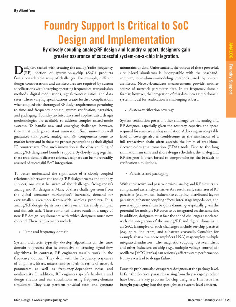
A typical RFIC design can be performed using UMC’s EMDM methodology (see Figure 3). The foundry’s advanced RFIC design solution promises even more benefits (see Figure 4). Rather than offer a solution that features a specific EDA company’s design flow, UMC provides a bundled solution of tools from a range of vendors. The combination of the EMDM methodology, advanced RF CMOS process design technology, and silicon-proven reference-design library vows to give designers a jumpstart into the design cycle (see Figure 5).
Figure 2: This high-frequency passive-component design kit includes a built-in set of spiral-inductor libraries and high-frequency passive components, such as metal-insulator-metal or metal-oxide-metal capacitors.
Figure 3: This methodology can be used in any typical RFIC design flow.
Figure 4: This solution, which targets RFIC design, features design tools from various vendors.
24 • December / January 2006 Chip Design • www.chipdesignmag.com
Foun
dry
Supp
ort
anal
og
By albert Yen
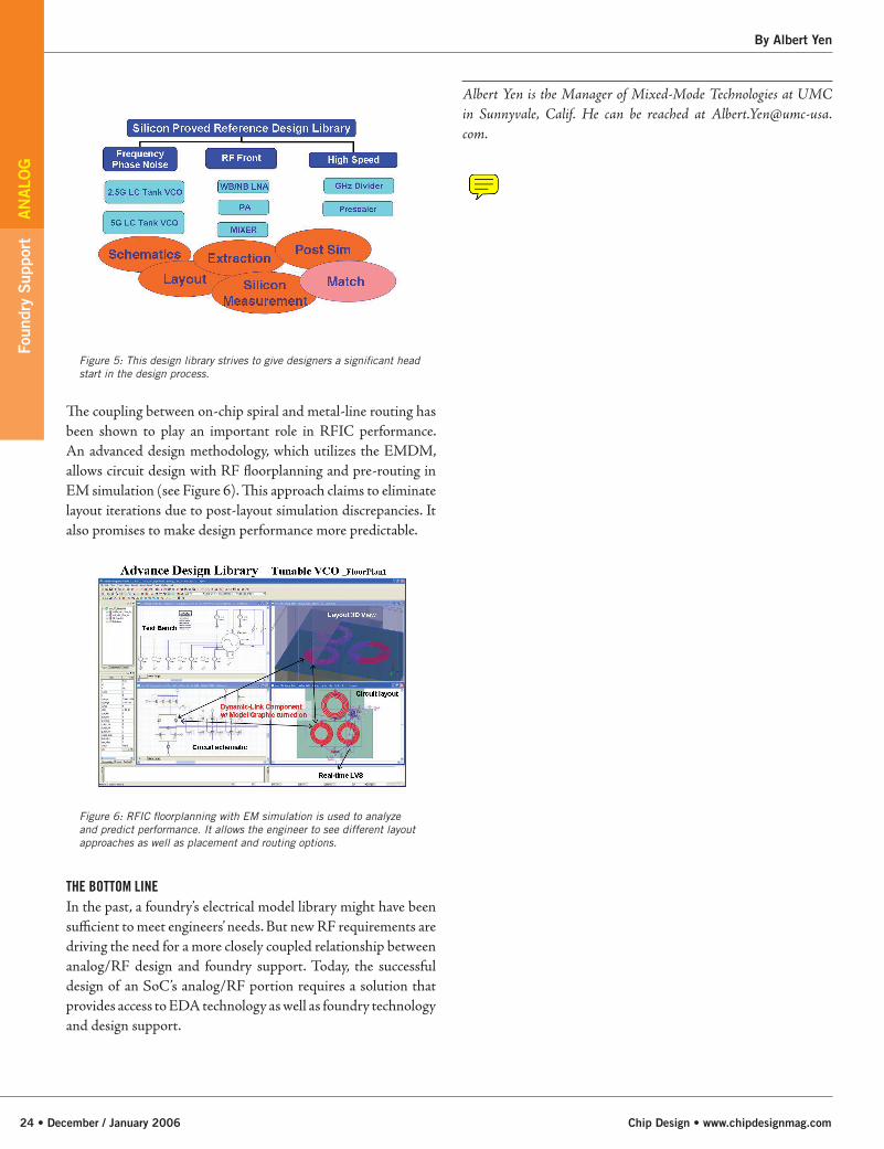
The coupling between on-chip spiral and metal-line routing has been shown to play an important role in RFIC performance. An advanced design methodology, which utilizes the EMDM, allows circuit design with RF floorplanning and pre-routing in EM simulation (see Figure 6). This approach claims to eliminate layout iterations due to post-layout simulation discrepancies. It also promises to make design performance more predictable.
the Bottom lIneIn the past, a foundry’s electrical model library might have been sufficient to meet engineers’ needs. But new RF requirements are driving the need for a more closely coupled relationship between analog/RF design and foundry support. Today, the successful design of an SoC’s analog/RF portion requires a solution that provides access to EDA technology as well as foundry technology and design support.
Figure 5: This design library strives to give designers a significant head start in the design process.
Albert Yen is the Manager of Mixed-Mode Technologies at UMC in Sunnyvale, Calif. He can be reached at [email protected].
Figure 6: RFIC floorplanning with EM simulation is used to analyze and predict performance. It allows the engineer to see different layout approaches as well as placement and routing options.
John
Note
Time for a Change Change is nothing new to the electronics industry. New technologies, processes and methodologies are constantly forcing engineers to re-evaluate existing approaches. The EDA industry is facing key changes as well. Traditional design processes are fragmented. Cross domain verification is often ineffective and, more often than not, designers must integrate analog and digital blocks manually. At the same time, the long simulation runtimes associated with modeling, extraction and re-simulation of parasitics are killing product development schedules. I believe EDA companies can shorten their customers’ time-to-productivity by helping them apply their EDA technology to the unique needs of each vertical market. The key to this new approach will be the development of design solutions tailored to efficiently create market-specific designs. What will these new solutions look like? Rather than a bundle of point technology, EDA companies must deliver verified design methodologies targeted at the key design challenges of vertical markets. These methodologies must be demonstrated on a segment representative design and enabled by a comprehensive suite of tools, platform flows and IP. The solutions must then go beyond that demonstration and map those methodologies to the customers’ specific needs – to their own designs. Finally, this capability must be delivered through results-driven consulting services. As part of this new approach, EDA companies must assume a new role as well. Instead of simply supplying tools, they must become a true partner with their customers, someone the product designer can trust to help work through these challenges, reduce risk, and shorten the developer’s time-to-productivity. Ultimately EDA companies must simplify the application of their technologies so their customers can focus their precious resources on design differentiation, not the design infrastructure. By taking a new approach that focuses on the unique challenges customers face in their particular vertical market, EDA companies can help their customers adapt to these new realities, build a tightly-focused design team capable of managing this new complexity, and bring higher quality products to market faster. By Kelly Perey, corporate vice president, Cadence Design Systems, Inc.