MRAM By Jeff Hanna Abstract‐ Magnetic Random Access memory holds the potential to replace all different types of memory as the only candidate for true “universal” memory. Memory is an element that is in every single computing device. As the need for smaller faster computers increases so does the need for scalable solutions. MRAM has evolved past the research and development stages and is now in production. Recent improvements have made this technology a nonvolatile, low power solution for many of today’s computing needs, especially for embedded systems. The fabrication techniques are comparable to current day silicon lithography processes making it easy to use current factories rather than building a completely new process. When MRAM is compared to current and prototypical technologies, it is visible that MRAM performs better. With the revenue created by the memory market expected to sky rocket, MRAM could grab a hold of a majority of the market share with revenues up to $16 billion in 2012. Table of Contents 1. Introduction 2. Basic Elements of MRAM 3. Fabrication 4. Comparison with Different Memories 5. Current Value in Memory Market 6. Conclusions
Transcript
MRAM
By Jeff Hanna
Abstract‐ Magnetic Random Access memory holds the potential to replace all different types of memory as the only candidate for true “universal” memory. Memory is an element that is in every single computing device. As the need for smaller faster computers increases so does the need for scalable solutions. MRAM has evolved past the research and development stages and is now in production. Recent improvements have made this technology a nonvolatile, low power solution for many of today’s computing needs, especially for embedded systems. The fabrication techniques are comparable to current day silicon lithography processes making it easy to use current factories rather than building a completely new process. When MRAM is compared to current and prototypical technologies, it is visible that MRAM performs better. With the revenue created by the memory market expected to sky rocket, MRAM could grab a hold of a majority of the market share with revenues up to $16 billion in 2012.
Table of Contents
1. Introduction 2. Basic Elements of MRAM 3. Fabrication 4. Comparison with Different Memories 5. Current Value in Memory Market 6. Conclusions
1. Introduction
Richard Feynman discussed the importance of small thinking back in 1959. Since then Moore’s Law predicted number of basic elements – transistors‐ on a microchip to double every 18 months. Experts wonder how long this trend can continue. Currently, line widths in these devices are shrinking down below 100nm. At this size, classical mechanical principles are overcome by quantum mechanical forces. One atom of helium is approximately 1 angstrom in diameter or 10nm. Intel claims that 32nm technologies are on the way. Currently computers operate at speeds upwards of 3 GHz. Due to the proliferation of battery powered embedded systems, power is needed to be conserved as much as possible in future devices. This paper investigates new trends evolving in the development of memory devices, specifically commercially available MRAM devices.
In 2005 the memory market totaled $29 billion with specific sectors as follows: DRAM $16bill, SRAM $4bill, FLASH $9bill. [1] This number is expected to sky rocket towards $150 billion in 2010. The current technologies face issues in scalability. DRAM is leaky, SRAM is big and FLASH is slow. Magnetic Random Access Memory (MRAM) has been considered as one of the most promising universal memory technologies due to its non‐volatility, fast speed, zero standby power, radiation hardness, and high density.[2] MRAM is a memory which the stored data are represented by a magnetization direction and the read operation is done by a resistance measurement. This implies that its operation relies on a magnetoresistance phenomenon.
Early MRAMs utilized the anisotropic magnetoresistance (AMR) effect. This was followed in 1988 by the discovery of a giant magnetoresistance effect allowed smaller elements with a higher output signal due to higher resistance and larger MR effect (5‐15%). This effect is utilized by current commercial products like HDD read heads and magnetic sensors. Improvements to this were realized in the revolutionary field of magnetic tunnel junctions (MTJ).[5]
These new technologies are based on 1 transistor 1 magnetic tunnel junction (1T1MTJ) which combines the need for separate memory/processor chips into one convenient package. Newly developed MRAM display 2T1MTJ and 5T2MTJ devices that operate at 200MHz and 500MHz respectively while utilizing a write line inserted MTJ to reduce the current.[8] Proposed uses for MRAM includes devices such as Aerospace and military systems, digital cameras, notebooks, smart cards, mobile telephones, cellular base stations, personal computers, battery‐backed SRAM replacement, data logging specialty memories, media players and book readers. [3] 2. Basic Elements of MRAM
Magnetic Random Access Memory (MRAM) stores data by magnetic storage elements, unlike conventional RAM technologies, which store data as electric charge or current. The key element of MRAM is the Magnetic Tunnel Junction (MJT) used for binary storage as seen in Figure 1. This MJT contains two ferromagnetic layers and one tunnel barrier layer. One ferromagnetic layer is fixed (reference layer) while the direction of the other ferromagnetic layer (free layer) can be changed by a driving current. The cell has an orientation of either a
Figure 1 ‐ Conceptual View of MJT
parallel low resistance state or an anti‐parallel high resistance state. This resistance change is called tunnel magnetoresistance (TMR), which is defined as !R/R = (RAP ! RP )/RP,, where RAP and RP are the resistance for antiparallel (AP) and parallel (P) magnetization configurations between the two ferromagnets.
Figure 2 ‐ TMR Ratio Evolution for Various Tunnel Barriers
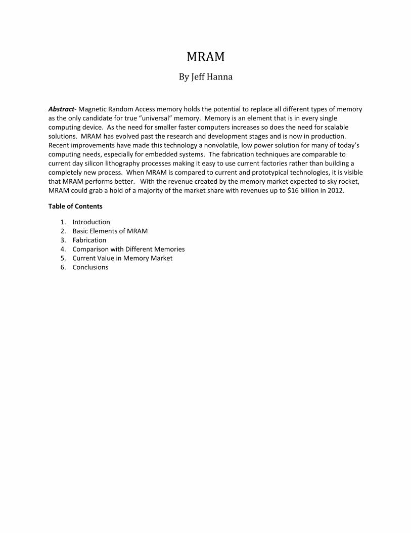
Recent work has been done to improve the TMR ratio with the MgO barrier becoming the leading contender for highest percentages as seen in Figure 2.[6] The evolution of the MTJ can be seen in Figure 2. Conventional MRAM, seen in Figure 3, uses a single step write operation and suffers from the most problems of the different types of MRAM. The write line requires a substantial current to the create magnetic field needed. This is less attractive for embedded systems where power needs to be conserved.
Figure 3 ‐ Conventional MRAM
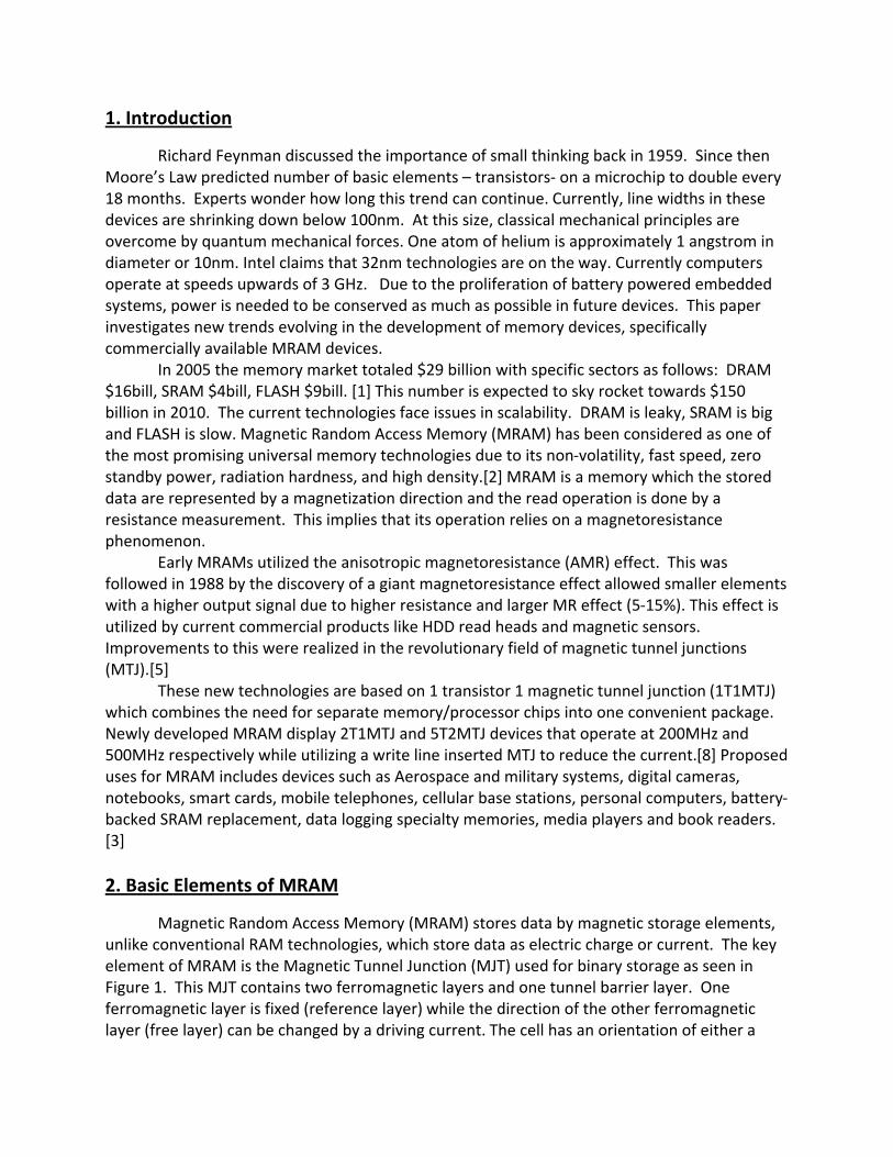
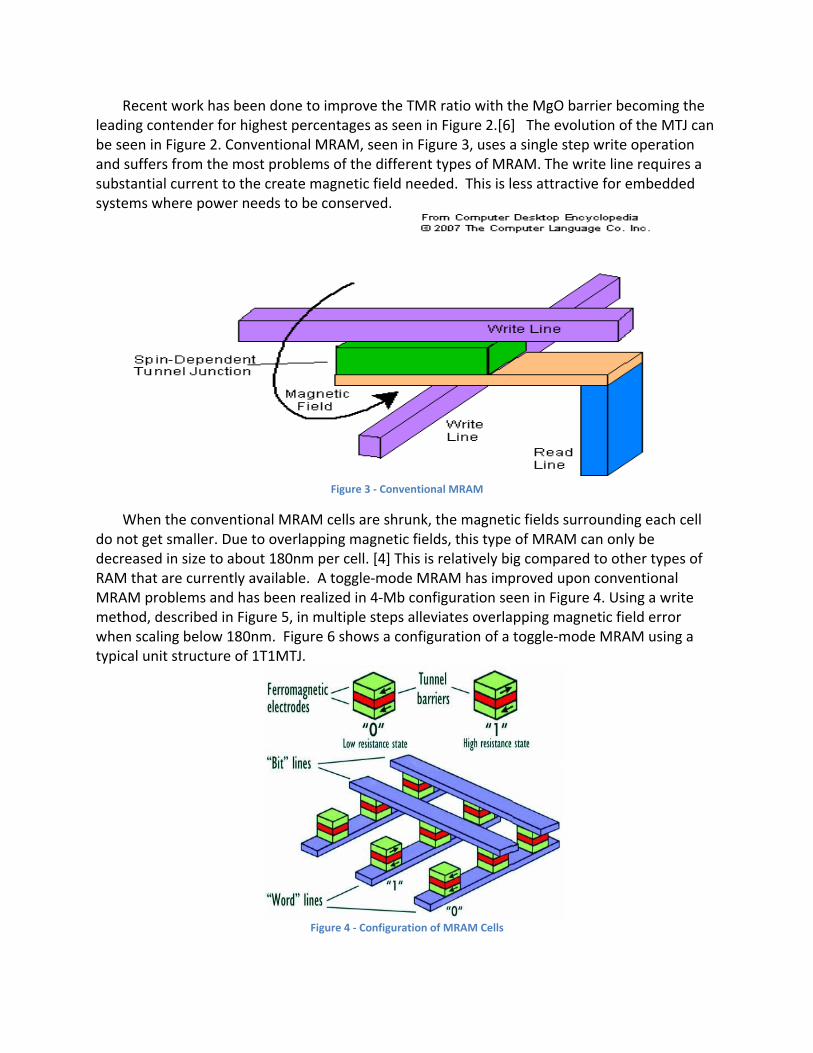
When the conventional MRAM cells are shrunk, the magnetic fields surrounding each cell do not get smaller. Due to overlapping magnetic fields, this type of MRAM can only be decreased in size to about 180nm per cell. [4] This is relatively big compared to other types of RAM that are currently available. A toggle‐mode MRAM has improved upon conventional MRAM problems and has been realized in 4‐Mb configuration seen in Figure 4. Using a write method, described in Figure 5, in multiple steps alleviates overlapping magnetic field error when scaling below 180nm. Figure 6 shows a configuration of a toggle‐mode MRAM using a typical unit structure of 1T1MTJ.
Figure 4 ‐ Configuration of MRAM Cells
Figure 5 ‐ Toggle Mode Write Process
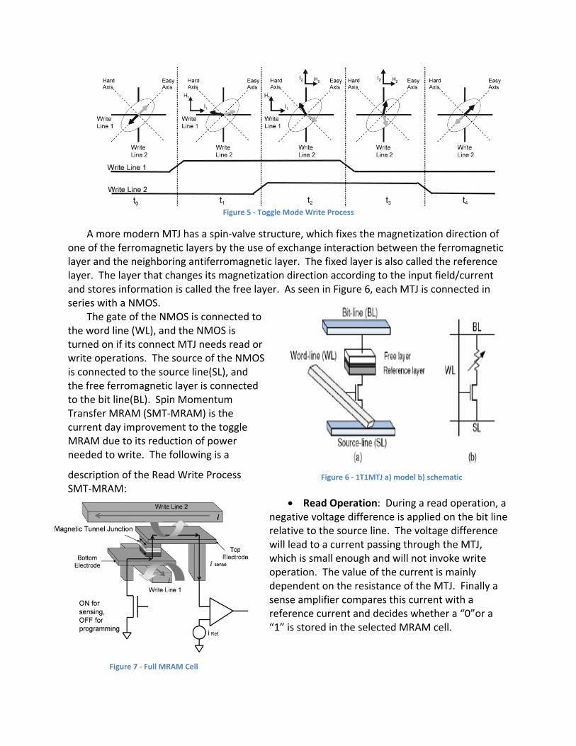
A more modern MTJ has a spin‐valve structure, which fixes the magnetization direction of one of the ferromagnetic layers by the use of exchange interaction between the ferromagnetic layer and the neighboring antiferromagnetic layer. The fixed layer is also called the reference layer. The layer that changes its magnetization direction according to the input field/current and stores information is called the free layer. As seen in Figure 6, each MTJ is connected in series with a NMOS.
The gate of the NMOS is connected to the word line (WL), and the NMOS is turned on if its connect MTJ needs read or write operations. The source of the NMOS is connected to the source line(SL), and the free ferromagnetic layer is connected to the bit line(BL). Spin Momentum Transfer MRAM (SMT‐MRAM) is the current day improvement to the toggle MRAM due to its reduction of power needed to write. The following is a
description of the Read Write Process SMT‐MRAM:
! Read Operation: During a read operation, a negative voltage difference is applied on the bit line relative to the source line. The voltage difference will lead to a current passing through the MTJ, which is small enough and will not invoke write operation. The value of the current is mainly dependent on the resistance of the MTJ. Finally a sense amplifier compares this current with a reference current and decides whether a “0”or a “1” is stored in the selected MRAM cell.
Figure 6 ‐ 1T1MTJ a) model b) schematic
Figure 7 ‐ Full MRAM Cell
! Write Operation: When writing “0” state into MRAM cells, positive difference is established between the source line and the bit line, and vice versa when writing “1” state. The current amplitude to reverse the direction of the free ferromagnetic layer is determined by the size of the MTJ and the writing pulse duration. The smaller the MTJ is or the longer the writing pulse is applied, the less critical switching current is needed.
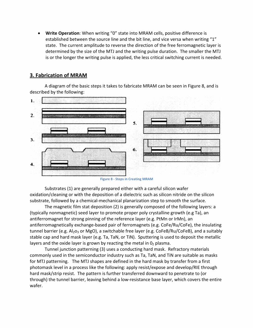
3. Fabrication of MRAM
A diagram of the basic steps it takes to fabricate MRAM can be seen in Figure 8, and is described by the following:
Figure 8 ‐ Steps in Creating MRAM
Substrates (1) are generally prepared either with a careful silicon wafer oxidation/cleaning or with the deposition of a dielectric such as silicon nitride on the silicon substrate, followed by a chemical‐mechanical planarization step to smooth the surface.
The magnetic film stat deposition (2) is generally composed of the following layers: a (typically nonmagnetic) seed layer to promote proper poly crystalline growth (e.g Ta), an antiferromagnet for strong pinning of the reference layer (e.g. PtMn or IrMn), an antiferromagnetically exchange‐based pair of ferromagnets (e.g. CoFe/Ru/CoFe), the insulating tunnel barrier (e.g. Al2o3 or MgO), a switchable free layer (e.g. CoFeB/Ru/CoFeB), and a suitably stable cap and hard mask layer (e.g. Ta, TaN, or TiN). Sputtering is used to deposit the metallic layers and the oxide layer is grown by reacting the metal in 02 plasma.
Tunnel junction patterning (3) uses a conducting hard mask. Refractory materials commonly used in the semiconductor industry such as Ta, TaN, and TiN are suitable as masks for MTJ patterning. The MTJ shapes are defined in the hard mask by transfer from a first photomask level in a process like the following: apply resist/expose and develop/RIE through hard mask/strip resist. The pattern is further transferred downward to penetrate to (or through) the tunnel barrier, leaving behind a low‐resistance base layer, which covers the entire wafer.
The dielectric encapsulation (4) protects the MTJs while at the same time forming the environment in which the MT wiring level will be created. The choice of encapsulation is determined from three requirements: a) it must not damage the MTJs b) it must adhere well to the substrate; and c) it should closely emulate the interlayer dielectrics that would be used in a fully integrated wafer process. The dielectric thickness is chosen such that it will be thick enough to provide the environment for the wiring level above the MTJs.
Planarization can be seen in Figure 8 (5). The wiring process adopted is the damascene copper wiring process and hence, the wafers generally undergo a gentle dielectric CMP process at this state. The purpose of the CMP is to remove topography from the surface that is cause by the underlying MTJs. This step is also the first check of the adhesion of the dielectric to the underlying metal films, as well as the cohesion of the metal films to each other.
The final step is the wiring seen in Figure 8 (6). This step comprises of a photomask‐
defined trench being etched into the dielectric with RIE. After the trench etching and suitable cleaning step, the wiring linear film is deposited, along with a thin copper see layer. This deposition is followed by the electroplating of copper to completely fill the trench and provide enough overburden so that the ensuing SMP step will planarize the metal coincident with the surface of the dielectric. A post‐polish cleaning of the wafers is the final preparation step before electrical testing.”[7] 4. Comparison of MRAM with other Memory Devices
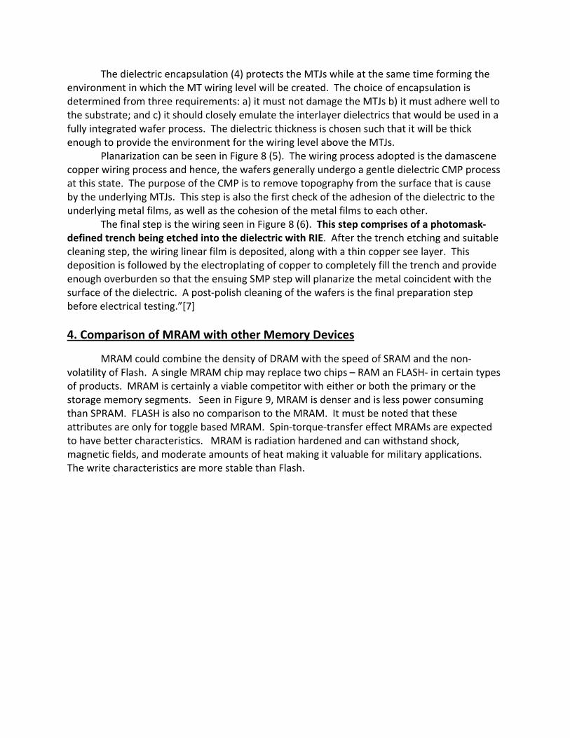
MRAM could combine the density of DRAM with the speed of SRAM and the non‐volatility of Flash. A single MRAM chip may replace two chips – RAM an FLASH‐ in certain types of products. MRAM is certainly a viable competitor with either or both the primary or the storage memory segments. Seen in Figure 9, MRAM is denser and is less power consuming than SPRAM. FLASH is also no comparison to the MRAM. It must be noted that these attributes are only for toggle based MRAM. Spin‐torque‐transfer effect MRAMs are expected to have better characteristics. MRAM is radiation hardened and can withstand shock, magnetic fields, and moderate amounts of heat making it valuable for military applications. The write characteristics are more stable than Flash.
Figure 9 ‐ MRAM comparison with current technology
The manufacturing process for MRAM is already familiar to the semiconductor industry and the technology is similar to that of GMR read heads for disk drives. Several MRAM firms are targeting their products for mobile computing and communication applications because of the alluring thermal and power consumption characteristics. While all of these benefits make this technology attractive, some significant problems must still be overcome.
MRAM is still an expensive solution. This is expected to change as volume production increases. Currently MRAM only proves the economical solution when either a MRAM chip will replace a Flash and a RAM chip or when a particular characteristic of MRAM, like radiation hardness needed in certain aerospace and defense applications, offers a clear and distinct competitive advantage.
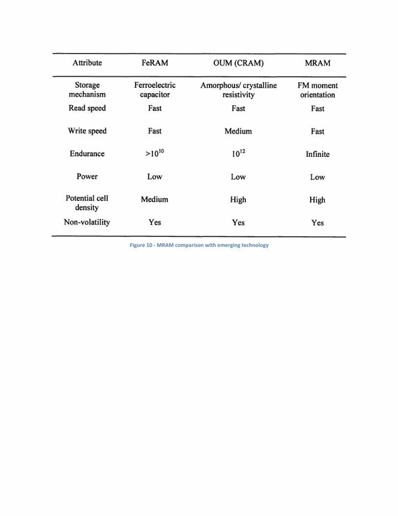
Also, scaling of the first generation of MRAM is well below the capacity of today’s conventional RAM or Flash chips. MRAM is currently in catch up mode, and this is expected for the next several years. Also, alternative memory technologies that are being pursued to find the ideal memory that have the attributes of non‐volatility, scalability and cost. Technologies that are future competitors are Ferroelectric RAM (FeRAM or FRAM) and Ovonic Unified Memory (OUM) are compared with MRAM in Figure 11. MRAM appears to be much superior to both FeRAM and OUM.
Figure 10 ‐ MRAM comparison with emerging technology
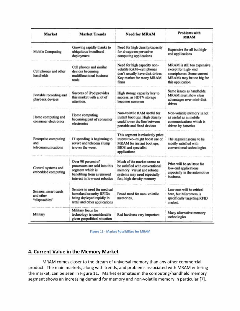
Figure 11 ‐ Market Possibilites for MRAM
4. Current Value in the Memory Market
MRAM comes closer to the dream of universal memory than any other commercial product. The main markets, along with trends, and problems associated with MRAM entering the market, can be seen in Figure 11. Market estimates in the computing/handheld memory segment shows an increasing demand for memory and non‐volatile memory in particular [7].
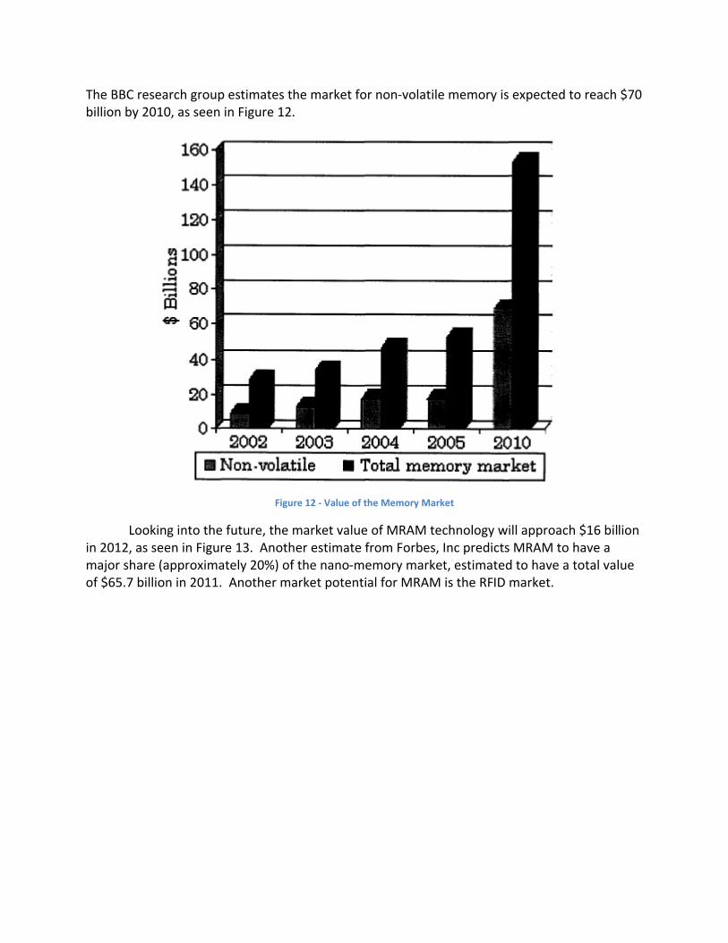
The BBC research group estimates the market for non‐volatile memory is expected to reach $70 billion by 2010, as seen in Figure 12.
Figure 12 ‐ Value of the Memory Market
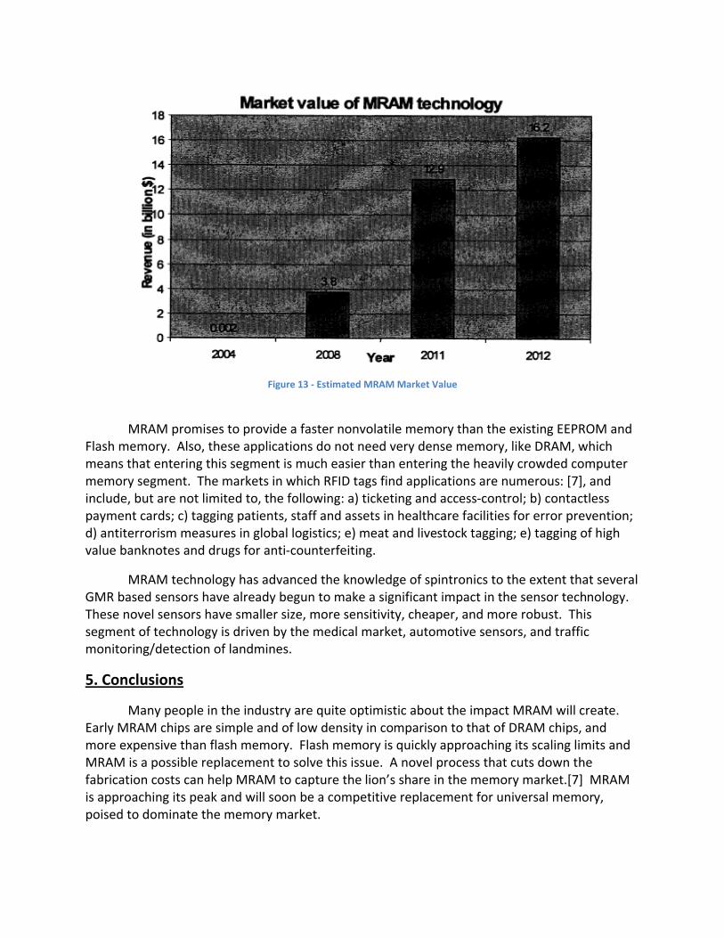
Looking into the future, the market value of MRAM technology will approach $16 billion in 2012, as seen in Figure 13. Another estimate from Forbes, Inc predicts MRAM to have a major share (approximately 20%) of the nano‐memory market, estimated to have a total value of $65.7 billion in 2011. Another market potential for MRAM is the RFID market.
Figure 13 ‐ Estimated MRAM Market Value
MRAM promises to provide a faster nonvolatile memory than the existing EEPROM and Flash memory. Also, these applications do not need very dense memory, like DRAM, which means that entering this segment is much easier than entering the heavily crowded computer memory segment. The markets in which RFID tags find applications are numerous: [7], and include, but are not limited to, the following: a) ticketing and access‐control; b) contactless payment cards; c) tagging patients, staff and assets in healthcare facilities for error prevention; d) antiterrorism measures in global logistics; e) meat and livestock tagging; e) tagging of high value banknotes and drugs for anti‐counterfeiting.
MRAM technology has advanced the knowledge of spintronics to the extent that several GMR based sensors have already begun to make a significant impact in the sensor technology. These novel sensors have smaller size, more sensitivity, cheaper, and more robust. This segment of technology is driven by the medical market, automotive sensors, and traffic monitoring/detection of landmines.
5. Conclusions
Many people in the industry are quite optimistic about the impact MRAM will create. Early MRAM chips are simple and of low density in comparison to that of DRAM chips, and more expensive than flash memory. Flash memory is quickly approaching its scaling limits and MRAM is a possible replacement to solve this issue. A novel process that cuts down the fabrication costs can help MRAM to capture the lion’s share in the memory market.[7] MRAM is approaching its peak and will soon be a competitive replacement for universal memory, poised to dominate the memory market.
References
[1] “Past, Present, and Future of MRAM”, Shehzaad Kaka, NIST Magnetic Technology presentation given July 2003.
[2] “Circuit and Microarchitecture Evaluation of 3D Stacking Magnetic RAM (MRAM) as a Universal Memory Replacement” Xiangyu Dong, Xiaoxia Wu, Guangyu Sun, Yuan Xie Pennsylvania State University Helen Li, Yiran Chen Seagate Technology (2007)
[3] http://en.wikipedia.org/wiki/MRAM
[4] “An Introduction to MRAM” Michael Haslett Computer Architecture, EE480 University of Detroit Mercy (2003) [5] “ Expectations of MRAM in comparison with other non‐volatile memory technologies” K.-M.H. Lenssen Philips Research Laboratories, Prof. Holstlaan [6] “Magneic Tunnel Junctions for Spintronic Memories and Beyond” Shoji Ikeda, Jun Hayakawa, Young Min Lee, Fumihiro Matsukura, Yuzo Ohno, Takahiro Hanyu, Member, IEEE, and Hideo Ohno, Member, IEEE
[7] “An Analysis of MRAM Based Memory Technologies” Rangarajan Vijayaraghavan (2006)
[8]” MRAM Cell Technology for Over 500‐MHz SoC” IEEE Journal of Solid‐State Circuits, Vol42,NO4, April (2007)


![Test System Requirements For Wafer Level MRAM Test SWTW-2004 Page [1] Test System Requirements For Wafer Level MRAM Test Raphael Robertazzi IBM/Infineon MRAM Development Alliance With](https://static.documents.pub/doc/80x56/5acbb8087f8b9a27628ba54b/test-system-requirements-for-wafer-level-mram-swtw-2004-page-1-test-system-requirements.jpg)


