+ All Categories
Home > Documents > by Mehmet Avci - University of Toronto

by Mehmet Avci - University of Toronto

Date post: 17-Feb-2022
Category:
Upload: others
View: 1 times
Download: 0 times
Share this document with a friend
82
Early Dual Grid Voltage Integrity Verification by Mehmet Avci A thesis submitted in conformity with the requirements for the degree of Master of Applied Science Graduate Department of Electrical and Computer Engineering University of Toronto c Copyright by Mehmet Avci 2010
Transcript

Early Dual Grid Voltage Integrity Verification

by

Mehmet Avci

A thesis submitted in conformity with the requirements

for the degree of Master of Applied ScienceGraduate Department of Electrical and Computer Engineering

University of Toronto

c© Copyright by Mehmet Avci 2010

Early Dual Grid Voltage Integrity Verification

Mehmet Avci

Master of Applied Science, 2010

Graduate Department of Electrical and Computer Engineering

University of Toronto

Abstract

As part of power distribution network verification, one should check if the voltage fluc-

tuations exceed some critical threshold. The traditional simulation-based solution to

this problem is intractable due to the large number of possible circuit behaviors. This

approach also requires full knowledge of the details of the underlying circuitry, not

allowing one to verify the power distribution network early in the design flow. In this

work, we consider the power and ground grids together (i.e. dual grid) and formulate

the problem of computing the worst-case voltage fluctuations of the dual grid under

the framework of current constraints. Then, we present a solution technique in which

tight lower and upper bounds on worst-case voltage fluctuations are computed via

linear programs. Experimental results indicate that the proposed technique results in

errors in the range of a few mV . We also present extensions to single grid (i.e. only

power grid) verification techniques.

ii

Acknowledgments

It is a pleasure for me to thank the many people who made this work possible.

I would like to gratefully acknowledge the enthusiastic supervision of my advisor

Professor Farid N. Najm. Without his inspiration, great efforts to explain things

clearly and constant support, the development of this work would not have been

possible. Many thanks Professor for all your appreciated guidance and advice. I am

proud and honored to call myself your student. I want to thank you for teaching me

lessons I will always remember.

I would also like to thank Professors Jason Anderson, Manfredi Maggiore, and

Jianwen Zhu, from the ECE department of the University of Toronto for reviewing

this work.

I am also thankful to Nahi H. Abdul Ghani for his guidance and support. Thank

you Nahi for being an excellent mentor for me. Long nights of work were more

pleasant with your friendship and sense of humor. I am indebted to many colleagues

for providing a great and pleasant environment in which to learn and work. I am

especially grateful to Khaled R. Heloue, Sari Onaissi, Imad A. Ferzli, Meric Aydonat,

Ankit Goyal, Andrew Canis and Hratch Mangassarian. I wish them the best in their

endeavors.

I am also lucky to have the support of many good friends. My roommates, Aurelie

Levallois and Bernadett Zupka, deserve a special mention, as they shared with me

their smile and friendship during these two years. Thank you Emanuela, Rafael,

iii

Acknowledgements

Yago, Marion and Daian for all the pleasant time we had together. I wish you all the

best.

My biggest gratitude goes to my parents, Menduha and Ziya. They bore me, raised

me, loved me and taught me. Mom and Dad, thank you for all the support you have

given to me. I hope I made you proud. I also hope my sister is proud of me. Buket,

I always found comfort in your love and support. I am forever indebted to you.

Lastly, I offer my regards to all of those who supported me in any respect during

the completion of this work.

iv

Contents

List of Figures vii

List of Tables viii

1 Introduction 1

1.1 Motivation . . . . . . . . . . . . . . . . . . . . . . . . . . . . . . . . . 11.2 Objective . . . . . . . . . . . . . . . . . . . . . . . . . . . . . . . . . 41.3 Thesis Organization . . . . . . . . . . . . . . . . . . . . . . . . . . . . 4

2 Background 5

2.1 Introduction . . . . . . . . . . . . . . . . . . . . . . . . . . . . . . . . 52.2 Vector-based Analysis . . . . . . . . . . . . . . . . . . . . . . . . . . 82.3 Vector-independent Analysis . . . . . . . . . . . . . . . . . . . . . . . 132.4 Limitations . . . . . . . . . . . . . . . . . . . . . . . . . . . . . . . . 16

3 Dual Grid Model and Current Constraints 17

3.1 Introduction . . . . . . . . . . . . . . . . . . . . . . . . . . . . . . . . 173.2 Dual Grid Model . . . . . . . . . . . . . . . . . . . . . . . . . . . . . 173.3 The System Equations . . . . . . . . . . . . . . . . . . . . . . . . . . 183.4 Current Constraints . . . . . . . . . . . . . . . . . . . . . . . . . . . . 25

4 Worst-Case Voltage Fluctuation 28

4.1 Introduction . . . . . . . . . . . . . . . . . . . . . . . . . . . . . . . . 284.2 Exact Worst-case . . . . . . . . . . . . . . . . . . . . . . . . . . . . . 284.3 Lower and Upper Bounds . . . . . . . . . . . . . . . . . . . . . . . . 33

4.3.1 Vector of Lower Bounds . . . . . . . . . . . . . . . . . . . . . 334.3.2 Vector of Upper Bounds . . . . . . . . . . . . . . . . . . . . . 39

4.4 Implementation . . . . . . . . . . . . . . . . . . . . . . . . . . . . . . 464.4.1 Inverse Approximation Method . . . . . . . . . . . . . . . . . 464.4.2 Network Simplex Method . . . . . . . . . . . . . . . . . . . . 50

4.5 Experimental Results . . . . . . . . . . . . . . . . . . . . . . . . . . . 52

5 Extensions to Single Grid Verification 57

5.1 Introduction . . . . . . . . . . . . . . . . . . . . . . . . . . . . . . . . 575.2 Solution for Non-overlapping Global Constraints . . . . . . . . . . . . 57

5.2.1 Base Case . . . . . . . . . . . . . . . . . . . . . . . . . . . . . 575.2.2 General Case . . . . . . . . . . . . . . . . . . . . . . . . . . . 62

v

Contents

5.2.3 Experimental Results . . . . . . . . . . . . . . . . . . . . . . . 635.3 Solution for Tree-structured Global Constraints . . . . . . . . . . . . 64

6 Future Work and Conclusion 65

Appendices 67

A Matrix Equalities 68

References 71

vi

List of Figures

1.1 A 5-node grid . . . . . . . . . . . . . . . . . . . . . . . . . . . . . . . 31.2 Current configuration resulting in voltage overshoot for node A . . . . 3

2.1 A multiple-layer power distribution network [1] . . . . . . . . . . . . 62.2 Reduction of noise margins of CMOS circuits with technology scaling [1] 72.3 Power current requirements of high-performance microprocessors with

technology scaling [2] . . . . . . . . . . . . . . . . . . . . . . . . . . . 82.4 An RLC model of an on-chip power distribution network [3] . . . . . 92.5 A hierarchical model of a power distribution network [4] . . . . . . . 102.6 An instance of a random walk game [5] . . . . . . . . . . . . . . . . . 12

3.1 Macroblock model . . . . . . . . . . . . . . . . . . . . . . . . . . . . 183.2 The dual grid model . . . . . . . . . . . . . . . . . . . . . . . . . . . 193.3 A simple 5-node grid . . . . . . . . . . . . . . . . . . . . . . . . . . . 203.4 Voltages on the dual grid . . . . . . . . . . . . . . . . . . . . . . . . . 24

4.1 Absolute error comparison for all nodes of a 437-node grid . . . . . . 544.2 Absolute error comparison for all nodes of a 4285-node grid . . . . . . 544.3 Relative error comparison for all nodes of a 437-node grid . . . . . . . 564.4 Relative error comparison for all nodes of a 4285-node grid . . . . . . 56

vii

List of Tables

4.1 Runtime and accuracy comparison of AINV and SPAI . . . . . . . . . 504.2 Runtime comparison of the interior point method and the network

simplex method . . . . . . . . . . . . . . . . . . . . . . . . . . . . . . 534.3 Runtime and accuracy of lower and upper bound algorithms . . . . . 55

5.1 Effectiveness of the method given in claim 5.2.2 . . . . . . . . . . . . 63

viii

1 Introduction

1.1 Motivation

The feature size of modern integrated circuits (ICs) has been dramatically reduced in

order to improve speed, power and cost. The scaling of CMOS is expected to continue

for at least another decade and future nanometer circuits will contain billions of

transistors [6]. As CMOS technology is scaled, the power supply voltage will continue

to decrease [6]. With reduced supply voltages and more functions integrated into ICs,

the impact of voltage fluctuation is increasing and voltage integrity is becoming a big

concern for chip designers.

There are many sources of on-chip voltage fluctuations, such as IR-drop, Ldi/dt

drop, and the resonance between the on-chip grid and the package. Most available grid

verification techniques use some form of circuit simulation to simulate the grid. Such

an approach requires full knowledge of the current waveforms drawn by underlying

transistor circuitry. These waveforms would then be used to simulate the grid and

to find the voltage fluctuation at each node. However, since the number of possible

circuit behaviors is very large, one needs to simulate the grid for a large number of

vector sequences at each node, which is prohibitively expensive. Another disadvantage

of the simulation-based approach is that it does not allow the designer to perform early

grid verification, when grid modifications can be most easily done. To overcome these

problems, we will adopt the notion of current constraints [7] to capture the uncertainty

1

1 Introduction

about the circuit details and behaviors. Under these constraints, grid verification

becomes a problem of computing the worst-case voltage fluctuations subject to current

constraints.

In the literature, the ground grid has always been assumed to be symmetric to the

power grid. In [1], the authors claim that the power and ground grids have the same

electrical requirements and therefore the structures of these grids are often symmetric,

particularly at the initial and intermediate phases of the design. They show that

this symmetry can be exploited in a way to reduce the complexity of the power

delivery network. The original symmetric circuit is transformed into an equivalent

circuit, where circuit elements are replaced with equivalent symmetric networks. The

nodes on the axis of symmetry of the circuit are equipotential. These nodes are

referred to as a virtual ground. The resulting circuit model contains two independent

symmetric grids, and therefore the analysis of only one circuit is necessary. However,

the assumption that the power and ground grids are symmetric is not reliable, since

even in initial stages of the design, some regions of the power delivery network are

removed to make way for signal routing. This introduces non-symmetry in the grid,

which might lead to erroneous results if symmetry is assumed.

We note in particular that the presence of non-symmetry can cause the voltage on

a given node of the grid to fluctuate in both directions, i.e. voltage undershoot and

overshoot, even for an RC grid (for an RC model of the power grid, voltage levels

can normally only be below vdd, under the assumption that the circuit does not inject

current into the power grid [8]). To see why, consider the simple unsymmetrical 5-

node grid shown in Figure 1.1. Figure 1.2 shows the current waveform assigned to

the current source in the circuit and the node voltage at node A as a result of an

HSPICE simulation. The simulation shows an overshoot where the node voltage at

node A goes above vdd. Excessive overshoots have effect on hold time requirements

2

1 Introduction

Figure 1.1: A 5-node grid

0 20 40 60 80 1000

10

20

30

40

50

60

time(ps)

curr

ent(

mA

)

0 20 40 60 80 1000.9

0.95

1

1.05

1.1

1.15

time(ps)

volta

ge(V

)

Figure 1.2: Current configuration resulting in voltage overshoot for node A

of ICs, and can cause oxide degradation. Therefore, one needs to verify the power

and ground grids together (i.e. a dual grid verification) in order to capture realistic

voltage fluctuations.

Previous work [7], [8], [9] have dealt with early vectorless single grid verification

for resistive-only, RC and RLC grids. However, the previous verification techniques

become prohibitive even for medium size grids. Therefore, there is also a clear need

for verification tools that can make checking a grid feasible and practical proposition.

3

1 Introduction

1.2 Objective

The goal of this work is to present a dual grid voltage integrity verification technique

that checks for voltage fluctuation violations early in the design flow to ensure proper

circuit performance. The problem will be solved under the assumption that we have

some knowledge about the circuit that will allow us to formulate some current con-

straints. We believe that this type of constraint can be obtained by previous design

expertise and power density (watts/µm2) for the target process technology, and there-

fore are a suitable way to handle uncertainty about the underlying circuitry. We will

model the power distribution network as an RC dual grid. The problem of dual grid

verification under these constraints will be finding the worst-case voltage fluctuations

for each node on the dual grid. We will also develop additional methodologies for

single grid verification to reduce the complexity of the problem.

1.3 Thesis Organization

This thesis is organized as follows: chapter 2 familiarizes the reader with power

distribution network verification techniques and methodologies that can be found

in the literature. Chapter 3 presents the mathematical modeling of the RC dual

grid. This chapter also describes the concept of current constraints and clarifies how

they are useful as a part of the verification problem. In chapter 4, we formulate the

verification problem, and propose an efficient solution for the lower and upper bounds

on the worst-case voltage fluctuations of the dual grid. We discuss further extensions

to single grid verification techniques in chapter 5. Finally, chapter 6 presents potential

future work and concludes the thesis.

4

2 Background

2.1 Introduction

Power distribution networks in modern ICs are typically structured as a multiple-layer

metallic grid. In such a grid straight power/ground lines in each metal layer span the

entire die area. The power/ground lines alternate in each layer, and are orthogonal

to the lines in the adjacent layers. At overlap locations, vias are used to connect

a power (ground) line to another adjacent power (ground) line. The concept of the

power distribution network is shown in Figure 2.1, where only three metal layers are

shown. Power lines are indicated in dark grey and ground lines are indicated in light

grey.

When there is no circuit activity, the voltage on power and ground lines are equal

to the supply voltage level (vdd) and ground (0), respectively. However, the volt-

age levels fluctuate due to current loads, grid parasitics, and resonance between the

on-chip grid and the package. If the power supply voltage drops too low and the

ground voltage rises too high, the functionality and the performance of the circuit

will detoriate. Alternatively, excessive overshoots in power supply voltage and drops

in ground voltage can cause electromigration, affecting circuit reliability. These prob-

lems become more important in modern ICs, since the noise margins are reduced as

shown in Figure 2.2. Current requirements of high-performance microprocessors also

increase as shown in Figure 2.3. Therefore, the power distribution networks must be

5

2 Background

Figure 2.1: A multiple-layer power distribution network [1]

designed to minimize the voltage fluctuations, thereby keeping the local voltage level

within noise margins.

An important part of the on-chip interconnect resources is used to ensure the

voltage integrity. The global on-chip power distribution networks are designed at the

early stages of the design flow, when little is known about the underlying circuitry.

Modifying the global on-chip power distribution network at the late stages of the

design flow is prohibitively expensive, since it will require a complete redesign of the

surrounding global signals [1]. Therefore, power distribution networks are more likely

to be overdesigned [10], sometimes using more than a third of the on-chip interconnect

resources [11], [12].

The problems discussed so far made the signal integrity of the power supply an im-

portant concern of the chip designers. Traditional circuit simulators such as SPICE

are not able to simulate the grid because of computational time and memory lim-

itations. Hence, the research focus has been on developing efficient tools that can

validate the voltage fluctuations of a modern IC design in a reasonable computa-

tional time.

Two approaches have been used for power distribution network verification: vector-

6

2 Background

Figure 2.2: Reduction of noise margins of CMOS circuits with technology scaling [1]

based and vector-independent approaches. They both use linear circuit elements to

model the power distribution network as shown in Figure 2.4. The vector-based ap-

proach uses sequence of input vectors in order to generate a set of currents drawn by

the underlying circuitry. Then, it uses this set of currents to solve for the voltage fluc-

tuation. The vector-independent approach relies on the constraints that are bounds

on the grid currents, and tries to find the worst-case voltage fluctuations under these

constraints. In the following two sections, we will review several power distribution

network verification techniques belonging to these two approaches. We first start with

the vector-based approach. Then, we will discuss the vector-independent approach.

7

2 Background

Figure 2.3: Power current requirements of high-performance microprocessors withtechnology scaling [2]

2.2 Vector-based Analysis

The vector-based techniques combine the circuit model of a power distribution net-

work with time dependent worst-case current loads to obtain a linear model of the

power distribution network. This linear model is typically described using modi-

fied nodal analysis (MNA) method [13], which defines a system of linear differential

equations. Using numerical methods for solving differential equations, the system of

differential equations is reduced to a system of linear equations. Then the system of

linear equations are numerically solved using several linear system solution methods.

These methods are classified into direct and iterative methods. The direct methods

first factorize the the coefficient matrix, and then using the same factorization, the

solution at each simulation time step is obtained by forward and backward substitu-

tion. Iterative methods do not factorize the coefficient matrix, instead they solve the

8

2 Background

Figure 2.4: An RLC model of an on-chip power distribution network [3]

linear system of equations through a series of successive approximations. Since the

same factorization can be used for the substitution procedure, the direct methods are

more suitable for the simulation of the grid for a large number of time steps. When

the memory is insufficient to store the factorization matrices, iterative methods are

more efficient to solve the required system of equations. The switching currents of

cells and gates are obtained by assigning some kind of input vectors to a design in

order to simulate the voltage fluctuations on the grid.

In the literature, the research is focused on reducing the grid simulation time. The

methods such as macromodeling techniques [4], multigrid techniques [14], [15], [16],

[17], [18], and random walk algorithms [5] focus on reducing the computational com-

plexity of the grid simulation.

The macromodeling approach presented in [4] uses the hierarchical structure of the

grid to speed up the simulation engine. This macromodeling technique is shown in

Figure 2.5. The grid is divided into a global grid and local grids. Port nodes connect

local and global grids. The local grids are replaced by multiport linear elements.

These multiport elements have the same relation between their inputs and outputs

9

2 Background

Figure 2.5: A hierarchical model of a power distribution network [4]

as the voltages and currents on the local grid. The local grids are represented by the

following linear equation:

i(t) = Av(t) + S (2.1)

where i(t) is the ports current vector, A is the ports admittance matrix. v(t) is the

vector of voltages at the ports, and S is a constant vector of current sources that map

all the current sources internal in a local grid to the port nodes. The set (A, S) defines

the macromodel of the local grid. The characteristic equations of each macromodel

are stamped into the MNA equations of the global grid. The MNA equations are

solved to obtain the global grid voltages. These global grid voltages are then used to

obtain port currents using (2.1). Using port currents, one can solve for the internal

node voltages of the local grids.

The proposed partitioning scheme keeps the local grids sparse, thereby allowing

the efficient simulation of the grid. The experimental results in [4] show that the

problem size can be significantly reduced, if the user is concerned for a particular

region of the grid. However, the simulation of the full grid using this technique

10

2 Background

requires more time than a flat simulation. Since the voltages of the local grids can

be solved independently from each other, this method allows for parallelization of the

simulation.

The technique presented in [5] uses the method in statistics known as random walks.

The authors first analyze a resistive-only model of the grid. Using this model, the

voltage at any node x of the grid becomes:

vx =

d(x)∑

i=1

gi∑d(x)

i=1 gi

vi −ix

∑d(x)i=1 gi

(2.2)

where d(x) is the number of neighboring nodes of node x, gi is the conductance

between nodes i and x, and ix is the value of the current source at node x. In

addition to (2.2), the grid is represented as an undirected graph, where each node

is represented by a vertex, and each branch by an edge. They calculate the voltage

fluctuation at node x, a walk is started from that node as shown in Figure 2.6. This

walk tries to cross any of edges connected to node x. Defining the probability of going

to node i from x as px,i, we have:

px,i =

d(x)∑

i=1

gi∑d(x)

i=1 gi

(2.3)

Letting mx to define the amount one has to pay before leaving node x, we have:

mx =

d(x)∑

i=1

ix∑d(x)

i=1 gi

(2.4)

When one reaches a vdd node, the algorithm stops, and the voltage fluctuation at

node x is set to the average that one has to pay to get to a vdd node. Since this is a

random walk algorithm, a certain number of experiments has to be performed. The

average voltage fluctuation obtained in these experiments is used to approximate the

voltage fluctuation at node x.

11

2 Background

Figure 2.6: An instance of a random walk game [5]

The experimental results for resistive only grids show that the algorithm achieves a

3X speedup compared to the hierarchical analysis in [4]. The authors also show that

the algorithm can be extended to handle transient simulation of both RC and RLC

models of the grid.

The work presented in [14] uses a multigrid technique for efficient simulation of

the grid. This technique coarsens the grid by removing some of its nodes according

to a node selection criteria. First the grid is mapped to a coarser grid, then the

new reduced problem is solved using a simulation tool, and finally the results of the

simulation is mapped back to the original grid. Since the voltages on the removed

nodes of the original grid are interpolated using the voltages on the nodes in the

coarser grid, this method results in slightly inaccurate results. However, the results

in [14] show that the error is quite small, offering a significant speedup compared to

a direct solver using the original grid. Different approaches [15], [16], [17], [18] have

12

2 Background

been proposed to choose which nodes to remove, and they all work in a similar way

except the method in which they coarsen the grid.

The approaches discussed so far have at least two major drawbacks to be used

as verification tools. First, they assume that the complete structure of the under-

lying transistor circuitry is known. However, the power distribution networks are

designed early in the design process, before the details of the underlying circuitry

are known. Second, to find the worst-case voltage fluctuations under all different

current waveforms, we require exhaustive simulation of the grid for a large number

of input vector sequences. Thus, one usually simulates the grid for some input vector

sequences, which is not able to cover all the worst-case situations for the grid. Be-

cause of these reasons, recent research is focused on vector-independent techniques to

verify the grid to find the worst-case voltage fluctuations. We will summarize these

vector-independent techniques in the next section.

2.3 Vector-independent Analysis

In [7], the authors propose an early vector-independent power distribution network

verification technique. This approach assumes that only incomplete information of

the circuit currents is available early in the design flow. This incomplete information is

then formulated as current constraints. Some of these constraints (local constraints)

define upper bounds on currents drawn by underlying circuitry. Other constraints

(global constraints) define upper bounds on the sum of groups of currents drawn by

logic blocks. These constraints express the fact that certain groups of current sources

draw no longer than a certain level of current. They can be formulated using the

information that the known total power dissipation for that block does not exceed a

certain threshold.

13

2 Background

The authors verify the grid assuming a DC system. Under this assumption, the

grid is modeled as a purely resistive network whose equation is:

Gv = i (2.5)

where G is the grid conductance matrix, v is the vector of voltage drops, and i is the

vector of current sources representing the underlying circuitry. Under this model of

the grid, the verification problem becomes a linear optimization problem where the

vector of voltage drops is maximized subject to the current constraints. The resulting

linear program is solved using the simplex method, and the results show the voltage

drop distribution on the grid.

This paper presents the first vector-independent technique that used current con-

straints to verify the grid early in the design process. The voltage drop is the exact

worst-case voltage drop at any node of the grid under the given constraints and as-

suming the currents on the grid are DC. However, a drawback of this approach is the

assumption that the currents on the grid are DC. The transient currents can create

higher voltage fluctuations than DC currents.

The methods in [8], [9] extend the work of [7] to handle transient current sources

under DC current constraints. The technique presented in [8] assumes an RC model

of the grid and verifies the grid under transient currents. The system equation under

this model becomes:

Gv(t) + Cv(t) = i(t) (2.6)

where C is a diagonal matrix of node capacitances, G is the grid conductance matrix,

v(t) is the vector of voltage drops, and i(t) is the vector of current sources. The

time-discretized version of (2.7) becomes:

14

2 Background

(

G +C

∆t

)

v(t) =C

∆tv(t − ∆t) + i(t) (2.7)

An important difference of the transient system when compared to the DC system

is that the vector of voltage drops varies with time and is no more a fixed vector.

Therefore, the grid safety becomes a transient verification problem. The authors

in [8] propose an exact solution to the verification problem under transient currents.

However, this formulation leads to potentially large problems. As a result, they

propose an upper bound on the worst-case voltage drops of the grid. They also re-

formulate the optimization problem to develop a safety check algorithm that applies

a sufficient condition for the safety of the grid. The method in [9] extends the work

of [8] to handle the RLC model of the grid.

In [19], the authors build on the work in [7] by using macromodeling technique

presented in [4]. The grid is partitioned into small blocks where the behavior of each

block is abstracted away at its ports. This approach allows designers to focus only

on one section of the grid that needs to be verified. Results in [19] show that this

approach achieves around 10X to 20X speedup when compared to the flat verification

of the entire chip.

In [20], the authors propose an upper bound algorithm along with a geometric

approach to verify the grid under transient current sources. This approach results in

errors, however it achieves a significant speedup compared to the work in [8].

In [21], the authors present an efficient verification method for the RC model of

the grid based on a sparse approximate inverse technique. This method significantly

reduces the size of the linear programs while ensuring a user-specified over-estimation

margin on the exact solution. The technique takes advantage of the locality on the

grid by using the sparse approximate inverse technique and ignoring the insignificant

entries in the computed inverse.

15

2 Background

2.4 Limitations

While the previous works [7], [8], [19], [9], [20], [21] are good contributions to vector-

independent power distribution network verification, a serious limitation is the in-

ability to handle power and ground grids together. The presence of non-symmetry of

power and ground grids can cause the voltage on a given node of the grid to fluctuate

in both directions, i.e. voltage undershoot and overshoot. As a result, there is a need

for a transient verification of the power distribution network to check for the impact

of the non-symmetry of power and ground grids. This will be the main subject of

this thesis. A preliminary and short version of this thesis appeared in [22].

16

3 Dual Grid Model and Current Constraints

3.1 Introduction

This chapter presents the mathematical preliminaries for the analysis of the dual grid.

First, we present the model of the dual grid. This model will be used to get a set of

system equations that will be used in our verification technique. Then, we present

the notion of current constraints, and explain how they will be useful in our early

dual grid analysis.

3.2 Dual Grid Model

We consider an RC model of the dual grid where each branch is represented either by

a resistor or capacitor. We define the nodes that are on the power grid as power grid

nodes, and similarly, the nodes that are on the ground grid as ground grid nodes.

Resistors are located between two power grid nodes or between two ground grid

nodes, i.e. no resistor exists between a power and a ground grid node. In addition,

the capacitors are located only between power and ground grid nodes and, unlike

previous work, we assume that a node can have multiple capacitors.

One common simplification in the literature is to model the current drawn by the

underlying transistor circuitry in a logic block as a single current source. We usually

know the current drawn by a logic block, but that logic block is usually attached to

17

3 Dual Grid Model and Current Constraints

Figure 3.1: Macroblock model

multiple nodes in the grid. Therefore, modeling the current drawn by a logic block

as a single current source is not valid, and yields pessimistic voltage fluctuations. In

order to capture this notion, we introduce the model of a macroblock, which groups

multiple current sources into a single block as shown in Figure 3.1.

The macroblock model in Figure 3.1 captures the true behavior of a logic block,

in the sense that it draws current from multiple nodes. Note that we do not require

having the same number of current sources for power and ground grid nodes. However,

for each macroblock, we have to ensure that the current leaving power grid nodes must

equal the current entering ground grid nodes. This will be an important equality

constraint that defines the feasibility space of currents.

A simple dual grid is shown in Figure 3.2. Notice that the macroblock has multiple

connections to the grid, and that some nodes have multiple capacitors attached.

3.3 The System Equations

We start by using the MNA method for linear circuits containing dynamic elements,

and independent voltage and current sources [23]:

18

3 Dual Grid Model and Current Constraints

Figure 3.2: The dual grid model

G′x(t) + C ′x(t) = s(t) (3.1)

where G′ is the conductance matrix; x(t) is a vector of node voltages, and voltage

source and inductor currents; C includes the capacitance and the inductance terms,

and s(t) includes the contributions from the voltage and current sources. s(t) has

three different kind rows: 1) rows with a value of voltage, which correspond to nodes

that are connected to voltage sources, 2) rows with a value of current, which cor-

respond to nodes that are connected to current sources, and 3) rows with 0, which

correspond to all other nodes.

For our verification problem, we are only interested in the node voltages that are not

connected to voltage sources. Thus we do not need to know the voltage source currents

and the node voltages for the nodes that are connected to voltage sources (because

every voltage source is from a node to ground, the node voltages at voltage sources

19

3 Dual Grid Model and Current Constraints

Figure 3.3: A simple 5-node grid

are vdd). Since we assume that the dual grid is modeled as an RC network, we do not

have any inductor currents. Therefore, we can simplify the MNA system (3.1), similar

to [14]. To see how, consider the simple dual grid shown in Figure 3.3. Applying the

MNA formulation on this grid yields:

g1 −g12 1

−g21 g2 −g23

−g23 g3

g4 −g45

−g45 g5

1 0

︸ ︷︷ ︸

G′

x1(t)

x2(t)

x3(t)

x4(t)

x5(t)

x6(t)

︸ ︷︷ ︸

x(t)

+

c2 −c24

c3 −c35

−c42 c4

−c53 c5

︸ ︷︷ ︸

G′

x1(t)

x2(t)

x3(t)

x4(t)

x5(t)

x6(t)

︸ ︷︷ ︸

x(t)

=

0

−ia(t)

−ib(t)

ia(t)

ib(t)

vdd

︸ ︷︷ ︸

s(t)

(3.2)

Since there is only one voltage source in the dual grid in Figure 3.3, we only need one

KVL equation at node 1©. Therefore, there are 5 KCL equations which are the first

5 equations in the system, and there is one KVL equation which is the last equation.

gij is the conductance between two adjacent nodes and therefore; gij = gji; and cij is

defined as the capacitance between two adjacent nodes and therefore; cij = cji. The

diagonal entry gi of G′ is defined as the total conductance connected to node i; and

20

3 Dual Grid Model and Current Constraints

the diagonal entry ci of C ′ is defined as total capacitance connected to node i. Notice

that the remaining entries of G′ and C ′ are not shown, because they are all 0.

We can modify the system of equations by replacing vdd for the node voltage at

node 1©. Setting x1(t) = vdd, and changing the right hand side vector for the equations

which depend on x1(t), the system of equations becomes:

1

g2 −g23

−g23 g3

g4 −g45

−g45 g5

x1(t)

x2(t)

x3(t)

x4(t)

x5(t)

+

c2 −c24

c3 −c35

−c42 c4

−c53 c5

x1(t)

x2(t)

x3(t)

x4(t)

x5(t)

=

vdd

−ia(t) + g21vdd

−ib(t)

ia(t)

ib(t)

(3.3)

We can as well ignore the first equation, because it simply says x1(t) = vdd. This

leads to:

g2 −g23

−g23 g3

g4 −g45

−g45 g5

x2(t)

x3(t)

x4(t)

x5(t)

+

c2 −c24

c3 −c35

−c42 c4

−c53 c5

x2(t)

x3(t)

x4(t)

x5(t)

=

−ia(t) + g21vdd

−ib(t)

ia(t)

ib(t)

(3.4)

Therefore, (3.4) is sufficient to compute the node voltages for the nodes that are not

connected to voltage sources.

Now let the dual grid consist of n+α nodes where nodes 1, 2, . . . , n have no voltage

sources attached, and nodes (n + 1), . . . , (n + α) are connected to voltage sources.

Similar to above discussion, the system of equations that describes the network can

be written as:

Gu(t) + C ˙u(t) = i(t) + G0vdd(n) (3.5)

21

3 Dual Grid Model and Current Constraints

where G and G0 are n×n conductance matrices and C is an n×n capacitance matrix.

u(t) is an n×1 vector of node voltages except the nodes that are connected to voltage

sources. i(t) is n×1 vector of current sources and vdd(n) is an n×1 vector whose each

entry is equal to the value of the supply voltage. The node voltages u(t) are with

respect to some reference (datum) node that is part of the ground grid.

Let h be the number of nodes in the power grid, and l be the number of nodes in

the ground grid, so that h + l = n. We can rewrite (3.5) by partitioning the vector of

node voltages with respect to power and ground grid nodes, and reordering the rows

and columns of G, C, G0 and the entries of i(t) accordingly as follows:

Gp 0

0 Gg

up(t)

ug(t)

+

Cp N

NT Cg

up(t)

ug(t)

=

−ip(t)

ig(t)

+ G0vdd(n) (3.6)

Since no resistor exists between power and ground grid nodes, G can be partitioned

into two submatrices Gp (h × h matrix) and Gg (l × l matrix). ip(t) (h × 1 vector)

and ig(t) (l×1 vector) are non-negative vectors defining the current sources attached

to power and ground grid nodes, respectively. Since capacitors exist only between

power and ground grid nodes, Cp (h×h matrix) and Cg (l×l matrix) are non-negative

diagonal matrices, and N is an h × l non-positive matrix.

If we set all current sources to 0, ∀t, then up(t) = vdd(h) and ug(t) = 0, ∀t, where

vdd(h) is an h × 1 vector whose each entry is equal to the value of the supply voltage.

For this case, the system of equations becomes:

Gp 0

0 Gg

vdd(h)

0

= G0vdd(n) (3.7)

Substituting G0vdd(n) from (3.7) into (3.6) and rearranging the terms, we obtain:

22

3 Dual Grid Model and Current Constraints

Gp 0

0 Gg

up(t) − vdd(h)

ug(t)

+

Cp N

NT Cg

up(t)

ug(t)

=

−ip(t)

ig(t)

(3.8)

Defining vp(t) = vdd(h) − up(t) to be the vector of voltage drops at power grid nodes,

we can write (3.8) as two separate equations:

Gpvp(t) + Cpvp(t) − Nug(t) = ip(t) (3.9)

Ggug(t) + Cgug(t) − NT vp(t) = ig(t) (3.10)

In matrix notation, (3.9) and (3.10) can be combined to yield:

Gp 0

0 Gg

vp(t)

ug(t)

+

Cp −N

−NT Cg

vp(t)

ug(t)

=

ip(t)

ig(t)

(3.11)

In this notation, vp(t) is positive when power grid nodes experience undershoots and

ug(t) is positive when ground grid nodes experience overshoots as shown in Figure 3.4.

Now define:

G =

Gp 0

0 Gg

, v(t) =

vp(t)

ug(t)

C =

Cp −N

−NT Cg

, i(t) =

ip(t)

ig(t)

So that (3.11) becomes:

Gv + C ˙v(t) = i(t) (3.12)

23

3 Dual Grid Model and Current Constraints

t1 t2

0

Vdd

time

node

vol

tage

↑vp(t)

↓ug(t)

vp(t1) > 0

ug(t2) > 0

Figure 3.4: Voltages on the dual grid

Notice that the circuit described by (3.12) is the original dual grid, but with all the

voltage sources set to zero and the directions of current sources attached to the power

grid nodes reversed. Furthermore, this equation is useful, because now the current

vector i(t) is a non-negative vector and the matrix C consists of only non-negative

elements.

Now assume that only m of n nodes of the dual grid have current sources attached.

Then we can reorder the rows and columns of the matrices and the entries of the

vectors in (3.12) to yield:

Gv(t) + Cv(t) =

i(t)

0(n−m)

= i(t) (3.13)

where G and C are matrices of size n × n, that are simply reordered replicas of G

and C. i(t) is the vector of size m representing the current loads, and 0(n−m) is the

zero-vector of size n − m. Finally, using the backward Euler formula, (3.13) can be

discretized in time as:

24

3 Dual Grid Model and Current Constraints

Av(t) = Bv(t − ∆t) + i(t) (3.14)

where A = (G + C∆t

) and B = C∆t

.

3.4 Current Constraints

We adopt the notion of current constraints in order to perform verification of the dual

grid. This approach [7] does not require complete information about the currents

drawn by the underlying circuitry, and may be called a vectorless approach. The

currents are typically hard to specify for at least two reasons. First, the number of

combinations of possible current waveforms is very large, and simulation of a large

set of waveforms is very time-consuming. Second, the simulation approach does not

allow the designer to verify the grid early in the chip design. For the simulation,

the details of the underlying circuitry must be already known, but it might not be

available or complete early in the design, when most of the major changes in grid

characteristics can be most easily incorporated.

We use three types of constraints: local constraints, global constraints and equality

constraints. Local constraints define upper bounds on individual current sources.

They can be expressed mathematically as:

0 ≤ i(t) ≤ iL (3.15)

where iL is a vector of size m and stands for the peak value of currents that the

current sources can draw. In this paper, we restrict our work to the case of DC

constraints, i.e. the upper bound is fixed over time. However, note that it is only

the constraints that are DC, the currents themselves are transient. An alternative is

25

3 Dual Grid Model and Current Constraints

to use transient current constraints, which are more difficult to use in practice, both

from the user’s standpoint (supplying transient constraints) and the verification tools

that would deal with them.

Local constraints do not completely capture the behavior of the grid, because it is

never the case that all chip components draw their currents simultaneously. There-

fore, we need global constraints, which are upper bounds on the sums of groups of

current sources. They might represent the maximum current that the group of cur-

rent sources in each macroblock can draw or the peak total power dissipation of a

group of macroblocks. If we assume that we have µ global constraints, then they can

be expressed as:

0 ≤ Ui(t) ≤ iG (3.16)

where U is a µ × n matrix that consists only of 0s and 1s. If a 1 is present in a

row of U , it indicates that the corresponding current source is included in that global

constraint. Similar to the case of local constraints, iG is a constant time-independent

DC constraint, but the currents themselves are transient waveforms.

As previously mentioned, we need to ensure that the currents leaving the power

grid are equal to currents entering the ground grid, which we will call an equality

constraint. If we assume that we have γ macroblocks, then the equality constraints

can be expressed as:

Mi(t) = 0 (3.17)

where M is a γ×n matrix that only consists of 1s, -1s and 0s. For each macroblock, 1s

correspond to current sources that are attached to the power grid, and -1s correspond

to current sources that are attached to the ground grid.

26

3 Dual Grid Model and Current Constraints

To simplify the notation, we will use F to denote the feasible space of currents, so

that i(t) ∈ F if and only if it satisfies (3.15), (3.16) and (3.17) at all time.

27

4 Worst-Case Voltage Fluctuation

4.1 Introduction

This chapter presents our solution approach. Given a set of current constraints we

will show how to find worst-case voltage fluctuations at every node. In section 4.2,

we will see how we can solve the problem exactly, which will be shown to be too

expensive. In section 4.3, we will present an efficient technique for finding lower and

upper bounds on the worst-case voltage fluctuations at each node. We will discuss the

implementation details of the lower and upper bound in section 4.4. In section 4.5, we

give empirical data to show that the lower and upper bounds are tight, and therefore,

useful in practice.

4.2 Exact Worst-case

Our problem is to find, for every node, the worst-case node voltage fluctuation over

all possible currents in F . To simplify the notation, let E = A−1 and D = A−1B, so

that we can write (3.14) as:

v(t) = Dv(t − ∆t) + Ei(t) (4.1)

We first write the matrix E as follows:

28

4 Worst-Case Voltage Fluctuation

E = [e1, e2, . . . , en] (4.2)

where ei is the ith column of E. Now define:

H = [e1, e2, . . . , em] (4.3)

where H is n × m matrix formed by the first m columns of E. Since we know that

the last n − m elements in i(t) are 0, we can write (4.1) as:

v(t) = Dv(t − ∆t) + Hi(t) (4.4)

Now consider the case in which the grid had no stimulus for t ≤ 0, which leads to

v0 = v(0) = 0. Then, writing at time ∆t, 2∆t and 3∆t, we obtain:

v(∆t) = Dv0 + Hi(∆t) = Hi(∆t) (4.5)

v(2∆t) = Dv(∆t) + Hi(2∆t) = DHi(∆t) + Hi(2∆t) (4.6)

v(3∆t) = Dv(2∆t) + Hi(3∆t)

= D2Hi(∆t) + DHi(2∆t) + Hi(3∆t)

(4.7)

Repeating this procedure for any future time p∆t, we have:

v(p∆t) =

p−1∑

k=0

DkHi((p − k)∆t) (4.8)

At every point in time t ∈ [0, p∆t], the input vector i(t) must be feasible, i.e. we must

have i(t) ∈ F . Under these conditions, we are interested in the worst-case voltage

29

4 Worst-Case Voltage Fluctuation

fluctuations attained (separately) by each component of v(p∆t). In order to capture

this notion, we use the following notation, introduced in [21].

Suppose f(c) : Rn → Rn is a vector function whose components are denoted

f1(c), . . . , fn(c), and let A ⊂ Rn. Now, define a vector x ∈ Rn, such that, with

i ∈ {1, 2, . . . , n}, xi is the maximum of fi(c) over all c ∈ A. We will denote this by

the following operator:

x = emax∀c∈A

(f(c)) (4.9)

Notice that each component xi, ∀i = 1, . . . , n may be found separately by solving the

following maximization problem:

maximize: fi(c)

subject to: c ∈ A

(4.10)

Similarly, define a vector y ∈ Rn, such that yi is the minimum of fi(c) over all c ∈ A.

We will denote this by the following operator:

y = emin∀c∈A

(f(c)) (4.11)

and each component yi, ∀i = 1, . . . , n may be found separately by solving the following

minimization problem:

minimize: fi(c)

subject to: c ∈ A

(4.12)

Using the emax(·) and emin(·) operators, we can express the worst-case voltage fluc-

30

4 Worst-Case Voltage Fluctuation

tuation at all nodes at time p∆t by:

v+(p∆t) = emax∀i(t)∈F

(p−1∑

k=0

DkHi((p − k)∆t)

)

(4.13)

v−(p∆t) = − emin∀i(t)∈F

(p−1∑

k=0

DkHi((p − k)∆t)

)

(4.14)

where the notation ∀i(t) ∈ F means that, for every time point t ∈ [0, p∆t], the

current vector i(t) satisfies all the (local, global and equality) constraints. v+(t) is a

non-negative vector defining the worst-case voltage drops on power grid nodes and

the worst-case voltage overshoots on ground grid nodes, and similarly, v−(t) is a non-

negative vector defining the worst-case voltage overshoots on power grid nodes and

the worst-case voltage drops on ground grid nodes. We used a minus sign in front of

emin(·) operator in (4.14) to avoid confusion about the notion of the lower and upper

bounds in the rest of this work. Using v+(t) and v−(t), v(t) can be bounded as:

−v−(t) ≤ v(t) ≤ v+(t) (4.15)

Although the RC model is dynamic, i.e., its currents and voltages vary with time, the

constraints are DC and do not depend on time. Hence, F is the same for each time

step. With this, the components of (4.13) and (4.14) can be decoupled [21], leading

to:

v+(p∆t) =

p−1∑

k=0

emax∀i∈F

[DkHi

](4.16)

v−(p∆t) = −

p−1∑

k=0

emin∀i∈F

[DkHi

](4.17)

where i is simply an m × 1 vector of variables that satisfies the (local, global and

31

4 Worst-Case Voltage Fluctuation

equality) constraints, without reference to any particular point in time. This is an

important simplification of the problem, as it has the advantage that the number of

constraints for each optimization is fixed and does not span all previous time points.

The advantage of using the matrix H instead of E is clear now, since at each time

step one needs to compute multiplication of an n × n matrix with an n × m matrix

instead of two n×n matrices. Furthermore, the optimization variables do not include

the redundant variables.

Claim 4.2.1. emax∀i∈F

[DkHi

]≥ 0, ∀k

emin∀i∈F

[DkHi

]≤ 0, ∀k.

Proof. Let x∗ = emax∀i∈F

[DkHi

]and y∗ = emin

∀i∈F

[DkHi

]. Assume that the claim is not

true, i.e. x∗j < 0 and y∗

j > 0. Since i† = 0 is feasible, i.e. i† ∈ F , we can choose i†,

so that(DkHi†

)

j= 0 > x∗

j and(DkHi†

)

j= 0 < y∗

j , which is a contradiction. This

completes the proof.

Using (4.16), (4.17) and claim 4.2.1, and taking the difference in two consecutive time

steps, we have:

v+(p∆t) − v+((p − 1)∆t) = emax∀i∈F

[Dp−1Hi

]≥ 0 (4.18)

v−(p∆t) − v−((p − 1)∆t) = − emin∀i∈F

[Dp−1Hi

]≥ 0 (4.19)

meaning that v+(p∆t) and v−(p∆t) are monotone non-decreasing functions of the

time point p, for any integer p ≥ 1.

In practice, we are interested in the steady state solution where the system becomes

independent of the initial condition v(t) = 0, ∀t ≤ 0. Since the RC grid model is a

dynamical system with a limited memory of its past, the steady state solution can be

32

4 Worst-Case Voltage Fluctuation

obtained by evaluating (4.16) and (4.17) at points far away from the initial condition,

i.e. as p → ∞. Thus, the general solution to the problem is:

v+(∞) = limp→∞

p−1∑

k=0

emax∀i(t)∈F

[DkHi

](4.20)

v−(∞) = − limp→∞

p−1∑

k=0

emin∀i(t)∈F

[DkHi

](4.21)

4.3 Lower and Upper Bounds

Using (4.20) and (4.21) is intractable, because they have to be evaluated for a large

number of time steps until convergence is achieved and the emax(·) and emin(·)

operators require linear programs proportional to the number of nodes in the grid,

which for modern designs is in the order of millions. As an alternative, we propose

an efficient solution to compute lower and upper bounds on the worst-case voltage

fluctuations of the dual grid.

4.3.1 Vector of Lower Bounds

We will show that, for specific initial conditions, both v+(t) and v−(t) will be mono-

tone non-decreasing functions of time t. We have found that the DC verification

solution of the grid is a good initial condition, which satisfies the monotonicity prop-

erty.

Non-zero initial conditions

We start by investigating the impact of starting the verification with different (non-

zero) initial conditions on the worst-case voltage fluctuations. If we have the initial

condition v0 at time t = 0, then writing (4.4) at time ∆t and 2∆t, we have:

33

4 Worst-Case Voltage Fluctuation

v(∆t) = Dv0 + Hi(∆t) (4.22)

v(2∆t) = Dv(∆t) + Hi(2∆t)

= D2v0 + DHi(∆t) + Hi(2∆t)

(4.23)

This can be repeated, so that at any future time p∆t, we have:

v(p∆t) = Dpv0 +

p−1∑

k=0

DkHi((p − k)∆t) (4.24)

Because the RC grid is a stable linear system and because the backward difference

approximation used in (3.14) is absolutely stable [24], it follows that for i(t) = 0, ∀t

and any bounded initial condition v0, equation (4.24) converges to 0 as t → ∞. For

i(t) = 0, ∀t, the voltage on the grid at any time p∆t can be written as:

v(p∆t) = Dpv0 (4.25)

Writing (4.25) as p → ∞, we get:

v(∞) = limp→∞

v(p∆t) = limp→∞

Dpv0 = 0 (4.26)

Since (4.26) is valid for any bounded initial condition, it is clear that Dp → 0 as

p → ∞. We will use the following theorem [25] to conclude that this actually means

ρ(D) < 1, where ρ(D) is the magnitude of the largest eigenvalue of D, also called the

spectral radius of D.

Theorem 4.3.1. Let D be a square matrix. Then, the sequence Dk, for k = 0, 1, . . . ,

converges to zero if and only if ρ(D) < 1.

34

4 Worst-Case Voltage Fluctuation

It is easy to see that at steady state, i.e. as p → ∞, choosing a different initial

condition other than v0 = 0 does not have any impact on v(∞) , because of the fact

that Dp converges to zero as p → ∞. Therefore, (4.8) and (4.24) become equivalent

as p → ∞. Using the notation in the previous section and using the fact that F is

the same for each time step, we can express the worst-case voltage fluctuations at

time point p∆t with the initial condition v0 as:

v+(p∆t) = Dpv0 +

p−1∑

k=0

emax∀i∈F

[DkHi

](4.27)

v−(p∆t) = Dpv0 −

p−1∑

k=0

emin∀i∈F

[DkHi

](4.28)

A monotone non-decreasing v+(t)

Under the DC model of the dual grid, (3.13) becomes:

Gv = i (4.29)

Now let L = G−1 and let K to be a n × m matrix, which is obtained as the first m

columns of L, such that:

K = [l1, l2, . . . , lm] (4.30)

where li defines ith column of L. Using the matrix K, we can write v = Ki. Now

assume that we have the DC solution of the system as the initial condition, leading

to:

v0 = Ki0 (4.31)

35

4 Worst-Case Voltage Fluctuation

We define the voltage vector v0 to be feasible, if it satisfies (4.31) for a current vector

i0 ∈ F .

Claim 4.3.2. If v0 is feasible, then v+(p∆t) given in (4.27) is a monotone non-

decreasing function of the time point p, for any integer p ≥ 1.

Proof. The claim is true if we can show that v+(p∆t) ≥ v+((p−1)∆t), for any integer

p ≥ 1. Substituting v0 from (4.31) into (4.27), we obtain:

v+(p∆t) = DpKi0 +

p−1∑

k=0

emax∀i∈F

[DkHi

](4.32)

Substituting DpK from (A.9) (see claim A.0.3 in Appendix A) into (4.32), we get:

v+(p∆t) = (K −

p−1∑

k=0

DkH)i0 +

p−1∑

k=0

emax∀i∈F

[DkHi

](4.33)

Taking the difference in two consecutive time steps, we have:

v+(p∆t) − v+((p − 1)∆t) = emax∀i∈F

[Dp−1Hi

]− Dp−1Hi0 (4.34)

We see in (4.34) that the emax(·) operator assigns the maximum value to the first

term on the right-hand side over all i ∈ F , whereas the second term on the right-

hand side has the variables i0 ∈ F , which may not result in the optimal solution.

Therefore, we conclude that if v0 is feasible, then v+(p∆t) ≥ v+((p − 1)∆t), for any

integer p ≥ 1. This completes the proof.

DC initial condition

Using the notation (X)j to define jth row of a matrix X and incorporating (4.27), (4.28)

and (4.31), we can express the worst-case voltage fluctuation for the jth node at time

p∆t as:

36

4 Worst-Case Voltage Fluctuation

v+j (p∆t) = (DpK)ji0 +

p−1∑

k=0

max∀i∈F

(DkH)ji (4.35)

v−j (p∆t) = (DpK)ji0 −

p−1∑

k=0

min∀i∈F

(DkH)ji (4.36)

A good choice of i0 for a given node would be the current combination that leads to

the worst-case voltage fluctuation for that node under the DC model of the dual grid.

The worst-case voltage fluctuation for the jth node under the DC model is given by:

v+j = max

∀i∈F(K)ji (4.37)

v−j = −min

∀i∈F(K)ji (4.38)

Denote the optimal value of i of the maximization problem in (4.37) as i+j (m × 1

vector) and that of the minimization problem in (4.38) as i−j (m× 1 vector). Since G

is an M-matrix [21], its inverse consists of only non-negative elements, which means

that K is a non-negative matrix. Therefore, the result of the minimization problem

in (4.38) under non-negative current constraints will be 0, which leads to i−j = 0.

Using i+j and i−j as the initial current at t = 0 for the jth node, (4.35) and (4.36)

become:

v+j (p∆t) = (DpK)ji

+j +

p−1∑

k=0

max∀i∈F

(DkH)ji (4.39)

v−j (p∆t) = −

p−1∑

k=0

min∀i∈F

(DkH)ji (4.40)

37

4 Worst-Case Voltage Fluctuation

Algorithm 1 Lower Bound Algorithm

Inputs: K, D, H,F and ǫOutputs: v+

lb(∞) and v−lb(∞)

1: Compute v+ = emax∀i∈F

[Ki] and save i+j for each node

2: Set p = 0 and stop flag = false

3: while stop flag = false do

4: p = p + 1

5: for j = 1, . . . , n do

6: Compute v+j (p∆t) using (4.39) and v−

j (p∆t) using (4.40)

7: end for

8: if v+(p∆t) − v+((p − 1)∆t) < ǫ then

9: if v−(p∆t) − v−((p − 1)∆t) < ǫ then

10: Set stop flag = true

11: Set v+lb(∞) = v+(p∆t) and v−

lb(∞) = v−(p∆t)

12: end if

13: end if

14: end while

Lower bound

Algorithm 1 describes the computation of the lower bound vector in detail, based

on (4.39) and (4.40). Using claim 4.3.2 and claim 4.2.1, we can see that v+j (p∆t)

in (4.39) and v−j (p∆t) in (4.40) are monotone non-decreasing functions of the time

point p, for any integer p ≥ 1. Since we stop the main loop of Algorithm 1 for a

finite p, when v+(p∆t) − v+((p− 1)∆t) and v−(p∆t)− v−((p− 1)∆t) are less than a

threshold ǫ, then v+lb(∞) and v−

lb(∞) are clearly lower bounds on v+(∞) and v−(∞),

respectively.

Since D is a nonnormal matrix, the norm of Dp does not necessarily decreases with

increasing p [26]. Therefore, we cannot guarantee that v+(p∆t) − v+((p− 1)∆t) and

v−(p∆t) − v−((p − 1)∆t) decrease with increasing p. However, we did not encounter

this phenomenon in practice.

38

4 Worst-Case Voltage Fluctuation

4.3.2 Vector of Upper Bounds

Following an approach similar to [27], we compute an upper bound on the worst-case

voltage fluctuations of the dual grid. Although the upper bound in [27] was derived

for an RLC model of the power grid, it will be shown that it is also valid for the

dual grid model presented in this work. We will show that the upper bound at time

t can be obtained from the upper bound at time t − r∆t, where r represents a small

number of time steps, and that this means that the upper bound at infinity can be

written as a matrix-vector product. The matrix is the inverse of (I − P ), where P is

a matrix, that depends on r. The vector is obtained by r applications of the emax(·)

and emin(·) operators.

Define r to be a positive integer such that p/r is an integer. Grouping every r

consecutive terms in (4.8) leads to [27]:

v(p∆t) =

p/r−1∑

k=0

Dkr

[r−1∑

q=0

DqHi((p − q − kr)∆t)

]

(4.41)

Now define:

Q = Dr (4.42)

s(t) =

r−1∑

q=0

DqHi(t − q∆t) (4.43)

Using (4.42) and (4.43), we can write (4.41) as a recursive relation as:

v(t) = Qv(t − r∆t) + s(t), ∀t = r∆t, 2r∆t, . . . , p∆t (4.44)

where v(0) = v0 = 0, ∀t ≤ 0. Now define:

39

4 Worst-Case Voltage Fluctuation

s+(r)(t)

s−(r)(t)

=

emax∀i(t)∈F

s(t)

− emin∀i(t)∈F

s(t)

=

emax∀i(t)∈F

(r−1∑

q=0

DqHi(t − q∆t)

)

− emin∀i(t)∈F

(r−1∑

q=0

DqHi(t − q∆t)

)

(4.45)

Clearly, (4.45) depends on r time steps. However we know that the current constraints

are constant and that F is the same for each time point, then the result of computing

emax(s(t)) and emin(s(t)) would be the same for any t. We can therefore decouple

the components of (4.45) leading to:

s+(r)(t)

s−(r)(t)

=

emax∀i(t)∈F

(r−1∑

q=0

DqHi(t − q∆t)

)

− emin∀i(t)∈F

(r−1∑

q=0

DqHi(t − q∆t)

)

=

r−1∑

q=0

emax∀i∈F

[DqHi]

r−1∑

q=0

emin∀i∈F

[DqHi]

=

s+(r)

s−(r)

(4.46)

The upper and lower bounds on s(t) can be defined with the help of s+(r) and s−(r) as:

−s+(r) ≤ s(t) ≤ s−(r) (4.47)

Claim 4.3.3. Let R be the matrix of the element-wise absolute values of the entries

of Q. Let N be the element-wise non-negative matrix N = 12(R − Q), then for v+

ub(t)

and v−ub(t) such that:

v+ub(t)

v−ub(t)

=

Q + N N

N Q + N

v+ub(t − r∆t)

v−ub(t − r∆t)

+

s+(r)

s−(r)

(4.48)

we have: −v−ub ≤ v(t) ≤ v+

ub, ∀t = r∆t, 2r∆t, . . . , p∆t.

Proof. Since v0 = 0, ∀t ≤ 0, we assume the case at time t = 0 is satisfied as an

equality, i.e. v+ub(0) = v−

ub(0) = v0 = 0. Then, the claim is true by induction if we

40

4 Worst-Case Voltage Fluctuation

prove the following, ∀t = r∆t, 2r∆t, . . . , p∆t:

v+ub(t − r∆t) ≥ v(t − r∆t)

−v−ub(t − r∆t) ≤ v(t − r∆t)

⇒v+

ub(t) ≥ v(t)

−v−ub(t) ≤ v(t)

(4.49)

Assuming the left hand side of (4.49) is true and using the fact that Q + N and N

are non-negative matrices, we obtain:

−(Q + N)v−ub(t − r∆t) ≤ (Q + N)v(t − r∆t) ≤ (Q + N)v+

ub(t − r∆t) (4.50)

−Nv+ub(t − r∆t) ≤ −Nv(t − r∆t) ≤ Nv−

ub(t − r∆t) (4.51)

Summing up (4.50) and (4.51), we get:

−(Q + N)v−ub(t − r∆t) − Nv+

ub(t − r∆t) ≤ Qv(t − r∆t)

≤ (Q + N)v+ub(t − r∆t) + Nv−

ub(t − r∆t)

(4.52)

Summing up (4.52) with (4.47), and using (4.44) and (4.48), we obtain:

−v−ub ≤ v(t) ≤ v+

ub (4.53)

This completes the proof.

As a result, given bounds on v(t−r∆t), we can compute bounds on v(t) using (4.48).

Even though one can only compute the upper bound on voltage fluctuations that

are r time steps ahead in time, we are interested in the upper bound in the steady

41

4 Worst-Case Voltage Fluctuation

state case, i.e. when t → ∞. To simplify the notation, let w = [v+ub(t) v−

ub(t)]T and

z = [s+(r) s−(r)]

T and define the 2n × 2n matrix P by:

P =

Q + N N

N Q + N

(4.54)

In matrix notation, (4.48) becomes:

w(t) = Pw(t− r∆t) + z (4.55)

Writing (4.55) at every time step r∆t, 2r∆t, . . . , p∆t leads to:

w(r∆t) = z

w(2r∆t) = Pz + z

w(3r∆t) = P 2z + Pz + z

...

w(p∆t) = (P p/r−1 + . . . + P + I)z (4.56)

From (4.56), it is clear that the convergence of the upper bound at infinity depends

on the convergence of the matrix series (P p/r−1 + . . . + P + I) as p → ∞. The series

∑∞

q=0 Xq for a square matrix X is known to converge [25] if and only if ρ(X) < 1,

under which condition the series limit is (I − X)−1. Provided that ρ(P ) < 1, upper

bound at infinity converges to:

w(∞) = (I − P )−1z (4.57)

Now we will show that ρ(P ) < 1 is guaranteed with an appropriate choice of r. We

state without proof the following claim. For a proof, the reader is referred to [27].

42

4 Worst-Case Voltage Fluctuation

Claim 4.3.4. The set of eigenvalues of P , called the spectrum of P, is the union of

the spectrums of Q and R.

Therefore, the necessary condition for w(∞) to converge is that ρ(Q) < 1 and ρ(R) <

1. Now we will show that the spectral radius of Q is always less than 1. Denoting

the set of all eigenvalues of D by σ(D) and using Theorem 4.3.1, we can write:

max∀λ∈σ(D)

|λ| < 1 (4.58)

From the spectral mapping theorem [28], we know that if k is an integer, we have the

following relationship:

σ(Dk) = {λk : λ ∈ σ(D)} (4.59)

Thus, ρ(Dr) < 1, for any integer r, meaning that ρ(Q) < 1. The spectral radius of R

is not known, and is expensive to compute. We will now establish an upper bound on

the spectral radius of R. It is shown in [26], that if k is an integer, then the spectral

radius of kth power of a matrix X is bounded by any consistent matrix norm as:

ρ(X)k ≤ ‖Xk‖ (4.60)

As k → ∞, the inequality in (4.60) becomes equality so that we have:

limk→∞

‖Xk‖ = ρ(X)k (4.61)

Since we further have that ρ(D) < 1, this actually means:

limk→∞

‖Dk‖ = 0 (4.62)

It is implied in (4.62) that ‖Dk‖ decays asymptotically to zero with increasing k.

43

4 Worst-Case Voltage Fluctuation

Incorporating (4.59), (4.62) and (4.42), we see that for some value of r, any consistent

norm of Q = Dr will become less than 1. Now it remains to relate the norm of Q to

that of R. Actually, Q and R have the same norm for the following norms:

‖Q‖1 = max1≤j≤n

n∑

i=1

|qij| = ‖|Q|‖1 = ‖R‖1 (4.63)

‖Q‖∞ = max1≤i≤n

n∑

j=1

|qij| = ‖|Q|‖∞ = ‖R‖∞ (4.64)

‖Q‖F =

√√√√

n∑

i=1

n∑

j=1

|qij|2 = ‖|Q|‖F = ‖R‖F (4.65)

Therefore, a sufficient condition for the convergence of w(∞) is when the minimum

of ‖Q‖1, ‖Q‖∞ and ‖Q‖F is less than 1. If this condition is reached, (4.57) is used to

compute the upper bound on the worst-case voltage fluctuations.

Since I − P is not as sparse as the system matrix A, finding (I − P )−1 becomes

computationally very expensive. Instead, one may use LU-factorization of I − P to

find the upper bound at infinity as follows:

w(∞) = (I − P )−1z ⇒ (I − P )w(∞) = z (4.66)

If we denote LU-factorization by (I − P ) = LU , then w(∞) can be found by:

forward solve: Lx = z

backward solve: Uw(∞) = x

Since LU-factorization of I −P is also computationally expensive, we may use (4.55)

to compute the upper bound at infinity by a few matrix-vector products and vector-

44

4 Worst-Case Voltage Fluctuation

Algorithm 2 Upper Bound Algorithm

Inputs: D, H and FOutputs: v+

ub(∞) and v−ub(∞)

1: Set Q = I, s+ = 0 and s− = 0

2: while ‖Q‖1 ≥ 1, ‖Q‖∞ ≥ 1 and ‖Q‖F ≥ 1 do

3: s+ := s+ + emax∀i∈F

[QHi]

4: s− := s− − emin∀i∈F

[QHi]

5: Q := QD

6: end while

7: Set N =1

2(|Q| − Q)

8: Set P =

[Q + N N

N Q + N

]

9: Compute v+ub(∞) and v−

ub(∞) using (4.67)

vector additions. To see how, we write (4.55) at every time step r∆t, 2r∆t, . . . , p∆t

as:

w(r∆t) = y0 = z, y1 = Py0

w(2r∆t) = y1 + y0, y2 = P (Pz) = Py1

w(3r∆t) = y2 + y1 + y0

...

yp/r−1 = P (P p/r−2z) = Pyp/r−2

w(p∆t) = yp/r−1 + yp/r−2 + . . . + y2 + y1 + y0 (4.67)

We see from above sequence of equations that the upper bound at time point t = p∆t

can be easily computed with matrix-vector products and vector-vector additions.

Since limk→∞

‖P k‖ = 0, (4.67) will converge to a steady state value after a number of

time steps.

The computation of the upper bound on the worst-case voltage fluctuations is

45

4 Worst-Case Voltage Fluctuation

shown in Algorithm 2, in which we use the notation |X| to denote the matrix of the

element-wise absolute values of the entries of a matrix X.

4.4 Implementation

4.4.1 Inverse Approximation Method

It is obvious from section 4.3 that the inverse of the system matrix A is needed for

the computation of the lower and upper bounds, because D = A−1B. For the lower

bound, we need to invert the conductance matrix G as well as A. We now explain

how this can be efficiently done.

Power distribution networks have a mesh structure, where a node has a small

number of neighboring nodes. Such a structure results in a matrix (i.e. A or G), that

is sparse, symmetric, positive definite, and banded. In the literature, it is well known

that the inverse of a non-singular sparse matrix is dense. Especially, a matrix that

results from a mesh structrure has the inverse that is almost full. However, it is also

well known in the literature that the inverse of a sparse, symmetric positive definite

and banded matrix has entries whose values decay exponentially as one moves away

from the diagonal [29]. This fact is the main idea of constructing sparse approximate

inverse preconditioners to precondition large sparse linear systems when using an

iterative method such as conjugate gradient method. Sparse approximate inverse

preconditioners try to find a good sparse approximate inverse M , such that MA ≈ I,

where I denotes the identity matrix.

There are numerous sparse approximate inverse techniques in the literature. One

of them is SPAI [30], which is based on Frobenius norm minimization. SPAI starts

with an arbitrary initial matrix M and iteratively refines its columns by minimizing

the Frobenius norm ‖MA − I‖F . This technique has been applied to power delivery

46

4 Worst-Case Voltage Fluctuation

network verification in [21]. Another technique is called AINV [31], which is based

on the conjugate Gram-Schmidt (or A-orthogonalization) process. AINV has the

advantage of using the fact that the matrix whose inverse is to be approximated is

symmetric positive definite, while SPAI is a general sparse approximate preconditioner

for unsymmetric matrices.

In what follows, we will briefly explain the AINV method given in [31]. Assume

that A is an n × n symmetric positive definite matrix. It is shown in [31] that the

factorization of A−1 can be obtained from a set of conjugate directions z1, z2, . . . , zn

for A. By writing a set of conjugate directions in matrix form, we have:

Z = [z1, z2, . . . , zn] (4.68)

where Z is the matrix whose ith column is zi. Knowing a set of conjugate directions

for A, we can write:

ZT AZ = D =

d1 0 · · · 0

0 d2 · · · 0

......

. . ....

0 0 · · · dn

(4.69)

where di = zTi Azi. To obtain a factorization of A−1, we write:

A−1 = ZD−1ZT (4.70)

Notice in (4.70) that the inverse of A can be obtained easily if we know a set of

conjugate directions z1, z2, . . . , zn. In [31], a set of conjugate directions is constructed

by means of a conjugate Gram-Schmidt (or A-orthogonalization) process applied to

any set of linearly independent vectors v1, v2, . . . , vn. The Gram-Schmidt process is

47

4 Worst-Case Voltage Fluctuation

a method for orthogonalizing a set of vectors in an inner product space of size n.

It takes a finite, linearly independent set of vectors v1, v2, . . . , vn and generates an

orthogonal set u1, u2, . . . , un that spans the same inner product space n. For further

details on the Gram-Schmidt process, the reader is referred to [32].

Since the Gram-Schmidt process can be applied to any set of linearly independent

vectors, it is convenient to choose vi = ei, where ei is the ith unit vector. From the

Cholesky factorization of A, we have:

A = LDLT (4.71)

where L is unit lower triangular, which leads to Z = L−T . Since the inverse of a unit

lower triangular matrix is a unit lower triangular matrix, it follows that Z is unit

upper triangular.

The factorization algorithm is given in Algorithm 3, in which the ith row of A is

denoted by (A)j . For a dense matrix this algorithm requires roughly twice as much

work as Cholesky factorization [31]. Although for a sparse matrix the cost can be

significantly reduced, the method is still expensive because the resulting matrix Z

tends to be dense. However, the sparsity can be preserved by reducing the amount

of fill-in occurring in the computation of z-vectors. Reducing the amount of fill-in

can be achieved by ignoring all fill-in outside selected positions in Z or by discarding

fill-ins whose magnitude is less than a tolerance δ.

In [33], the authors propose several strategies and special data structures to imple-

ment Algorithm 3 efficiently. We have used many aspects of their implementation and

we have made some modifications in their data structures to be able to access entries

in a matrix which is in compressed column storage (CCS) format. Since we do not

know the sparsity pattern of the inverse upfront, we have only used the strategy in

which we discarded fill-in occurring in the computation of z-vectors whose magnitude

48

4 Worst-Case Voltage Fluctuation

was less than δ = e−6.

Algorithm 3 AINV Inverse Factorization AlgorithmInputs: AOutputs: A−1

1: Let z(0)i = ei for 1 ≤ i ≤ n

2: for i = 1, . . . , n do

3: for j = i, . . . , n do

4: d(i−1)j = (A)jz

(i−1)j

5: end for

6: if i = n go to step 11

7: for j = i + 1, . . . , n do

8: z(i)j = z

(i−1)j −

d(i−1)j

d(i−1)i

z(i−1)i

9: end for

10: end for

11: Let zi = z(i−1)i and di = d

(i−1)i for 1 ≤ i ≤ n

12: Set Z = [z1, z2, . . . , zn]

13: Set D−1 =

1/d1 0 · · · 00 1/d2 · · · 0...

.... . .

...0 0 · · · 1/dn

14: Set A−1 = ZD−1ZT

We conducted several experiments to invert grid conductance matrices approxi-

mately with both SPAI and AINV. The computations were carried on a 64-bit Linux

machine with 8 GB memory. The implementation of SPAI is the same as in [21].

Table 4.1 summarizes the result of the experiments. Column 1 reports the number

of nonzeros in the original conductance matrix, whereas column 4 and 6 reports the

number of nonzeros in the approximate inverses computed using AINV and SPAI,

respectively. Column 7 shows the entry wise maximum difference between the ap-

proximate inverses computed by the two methods. Since the entry wise maximum

difference between the approximate inverses is not significant, the quality of both

inverses is comparable to each other. Looking at column 3 and 5, we see that AINV

49

4 Worst-Case Voltage Fluctuation

Grid AINV SPAI

nodes nonzeros runtime nonzeros runtime nonzeros entry wise max. diff.

352 1742 2.45 sec. 123904 9.58 sec. 123904 4.77 × 10⁻⁴

1019 5077 30.65 sec. 950679 234.53 sec. 920543 2.39 × 10⁻⁴

2145 10481 4.13 min. 3405684 19.74 min. 3259647 2.84 × 10⁻⁴

4594 10481 12.47 min. 8830532 40 min. 8543094 2.26 × 10⁻⁴

10580 50826 28.23 min. 16284736 2.45 h. 15924396 1.74 × 10⁻⁴

Table 4.1: Runtime and accuracy comparison of AINV and SPAI

is significantly faster than SPAI for our purposes. It is obvious that the inverse com-

puted with AINV method has more nonzeros than the original matrix. Although

we drop entries during the computation of z-vectors whose magnitude is less than

δ = e−6, the final stage of the Algorithm 3, which is A−1 = ZD−1ZT , results in

additional fill-in, and therefore the resulting approximate inverse has some entries

whose magnitude is less than δ. To reduce the number of nonzeros, one can drop

these insignificant entries after the computation of the approximated inverse.

Experimental results in [34] also show that AINV is more effective and faster than

the other approximate inverse methods. Therefore, we have adopted it for our imple-

mentation.

4.4.2 Network Simplex Method

We will show that the linear programs in our formulation can be efficiently solved

with the help of a network simplex method. Using the notation given in the previous

sections, we have the following linear program for each node:

50

4 Worst-Case Voltage Fluctuation

maximize / minimize: f(i)

subject to: 0 ≤ Ui ≤ iG

Mi = 0

0 ≤ i ≤ iL

(4.72)

where f(i) : Rn → R is the linear objective function of i. To simplify the notation,

we augment the matrices U and M into the matrix T , and we augment the vectors

iG and the zero-vector of size γ into the vector a:

T =

U

M

, a =

iG

0(µ)

where T is a matrix of size (µ + γ) × n, and a is a vector of size (µ + γ) × 1. With

this notation the linear program (4.72) can be rewritten as:

maximize / minimize: f(i)

subject to: 0 ≤ T i ≤ a

0 ≤ i ≤ iL

(4.73)

The constraint matrix T consists of entries which are 1s, -1s or 0s. It resembles the

node-arc incidence matrix (NAIM) of a network, in the sense that NAIM also has

entries which are 1s, -1s or 0s. This is the key observation that allows us to formulate

the optimization problem (4.73) as a network flow problem. In our optimization

problem, the equality constraints define flow conservation constraints of the network

flow problem, whereas local constraints define capacity constraints on the flow along

the edges in the network. Furthermore, global constraints define side constraints on

51

4 Worst-Case Voltage Fluctuation

the sum of the flows along the edges. For a more detailed discussion of network flow

problems, the reader is referred to [35].

Network flow problems can be efficiently solved with the help of the network simplex

method. Empirical results have shown that the method is significantly faster than

the standard simplex method, when applied to the same network problem [36]. Fur-

thermore, it is shown in [37] that significant computational speed up can be achieved

if closely related instances of network flow problems are solved sequentially. This

observation is quite beneficial for our problem in the sense that the feasibility space

of currents remains the same at each instance of the optimization problem. Thus, we

have the same optimization problem for each node except different objective functions.

Previous work for grid verification [19], [20] used the interior point method to

solve the required linear programs. To compare the runtime characteristics of the

interior point method and the network simplex method, we have conducted several

experiments to solve linear programs resulting from grid verification. To solve the

linear programs, the Mosek optimization package [38] was used. The computations

were carried on a 64-bit Linux machine with 8 GB memory. The results of the

experiments are presented in Table 4.2. Column 1 reports the size of the optimization

problem, whereas column 2 and 3 show the runtime to solve the problem using the

interior point method and the network simplex method, respectively. It can be seen

from Table 4.2 that the network simplex method is significantly faster than the interior

point method.

4.5 Experimental Results

To test our method, we have implemented Algorithms 1, 2, and 3 in C++. We have

set ǫ = e−5 to stop the main loop of Algorithm 1. To solve the required linear pro-

52

4 Worst-Case Voltage Fluctuation

Problem Interior Point Method Network Simplex Method

size runtime runtime

365 2.17 sec. 0.11 sec.

742 6.46 sec. 0.46 sec.

2143 28.89 sec. 2.73 sec.

6750 2.47 min. 15.92 sec.

14358 6.45 min. 46.29 sec.

24836 14.74 min. 1.56 min.

Table 4.2: Runtime comparison of the interior point method and the network simplexmethod

grams, we have used the hot-start option of the Mosek network simplex solver for

fast objective function switching. Several experiments were conducted on a set of

test grids, which were generated from user specifications, which include grid dimen-

sions, metal layers (M1-M9), pitch and width per layer, and C4 and current source

distribution. Minimum spacing and sheet and via resistances were specified accord-

ing to a 65 nm technology. A global constraint is specified for each macroblock, and

additional global constraints were specified covering the entirety of the grid area. The

computations were carried on a 64-bit Linux machine with 8 GB memory.

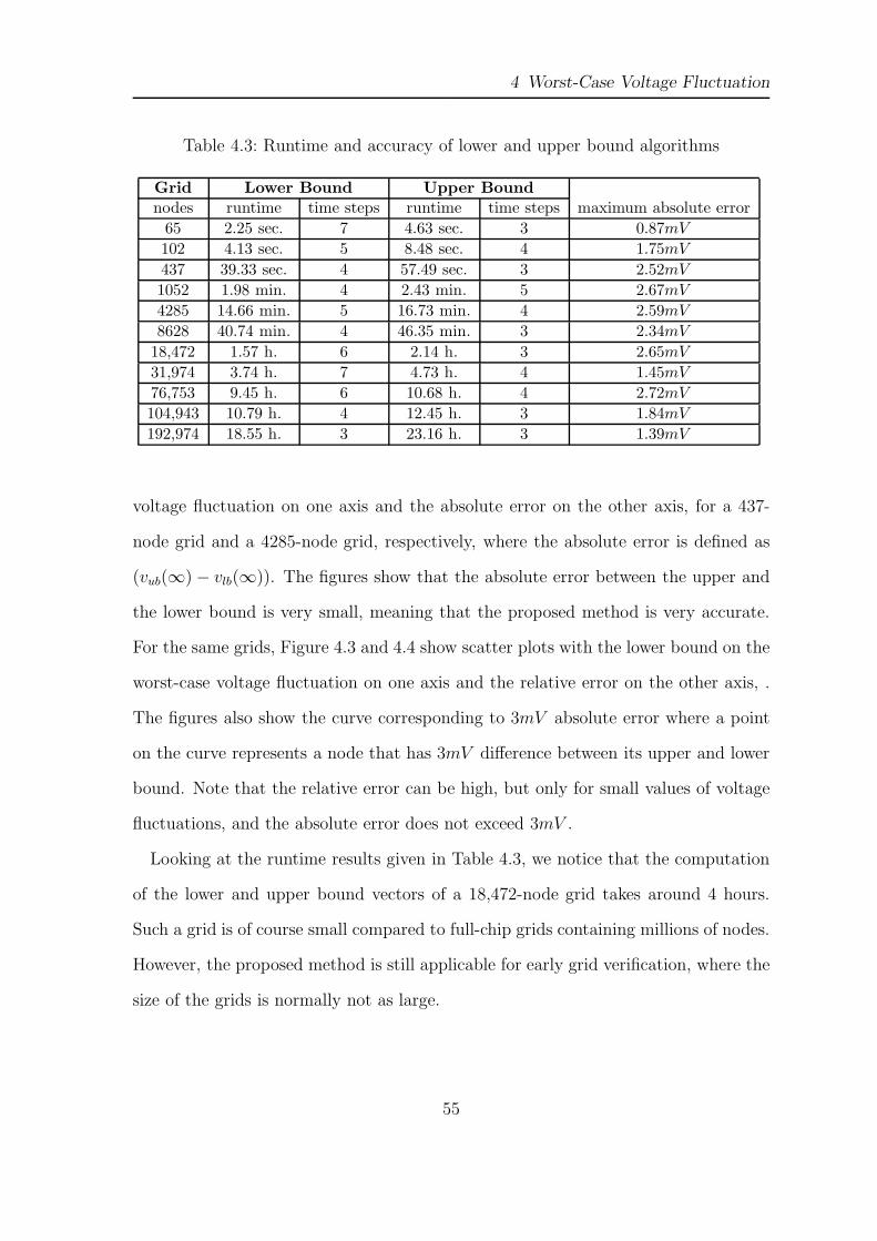
Table 4.3 shows the speed and the accuracy of our proposed solution technique for

the computation of the vectors of lower and upper bounds on the worst-case voltage

fluctuations. The results are compared with each other and the maximum absolute

difference between the upper and the lower bound vector is reported in column 6,

where the relative error is defined as (vub(∞) − vlb(∞))/vlb(∞). The results show

that our solution technique resulted in a maximum absolute error of 2.72mV across

all nodes of all test grids. The number of time steps shown in column 3 and 5 reports

the number of time steps for which the lower and upper bound algorithms converge.

The runtime for each one of two methods is also shown in the table.

Figure 4.1 and 4.2 show scatter plots with the lower bound on the worst-case

53

4 Worst-Case Voltage Fluctuation

0 0.02 0.04 0.06 0.08 0.1 0.12 0.14 0.160

0.5

1

1.5

2

2.5

3

3.5

lower bound on worst−case voltage fluctuation(V)

abso

lute

err

or(m

V)

Figure 4.1: Absolute error comparison for all nodes of a 437-node grid

0 0.02 0.04 0.06 0.08 0.1 0.12 0.14 0.160

0.5

1

1.5

2

2.5

3

3.5

lower bound on worst−case voltage fluctuation(V)

abso

lute

err

or(m

V)

Figure 4.2: Absolute error comparison for all nodes of a 4285-node grid

54

4 Worst-Case Voltage Fluctuation

Table 4.3: Runtime and accuracy of lower and upper bound algorithms

Grid Lower Bound Upper Bound

nodes runtime time steps runtime time steps maximum absolute error

65 2.25 sec. 7 4.63 sec. 3 0.87mV

102 4.13 sec. 5 8.48 sec. 4 1.75mV

437 39.33 sec. 4 57.49 sec. 3 2.52mV

1052 1.98 min. 4 2.43 min. 5 2.67mV

4285 14.66 min. 5 16.73 min. 4 2.59mV

8628 40.74 min. 4 46.35 min. 3 2.34mV

18,472 1.57 h. 6 2.14 h. 3 2.65mV

31,974 3.74 h. 7 4.73 h. 4 1.45mV

76,753 9.45 h. 6 10.68 h. 4 2.72mV

104,943 10.79 h. 4 12.45 h. 3 1.84mV

192,974 18.55 h. 3 23.16 h. 3 1.39mV

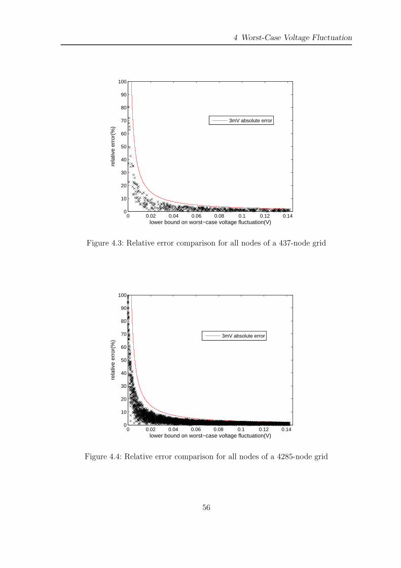
voltage fluctuation on one axis and the absolute error on the other axis, for a 437-

node grid and a 4285-node grid, respectively, where the absolute error is defined as

(vub(∞) − vlb(∞)). The figures show that the absolute error between the upper and

the lower bound is very small, meaning that the proposed method is very accurate.

For the same grids, Figure 4.3 and 4.4 show scatter plots with the lower bound on the

worst-case voltage fluctuation on one axis and the relative error on the other axis, .

The figures also show the curve corresponding to 3mV absolute error where a point

on the curve represents a node that has 3mV difference between its upper and lower

bound. Note that the relative error can be high, but only for small values of voltage

fluctuations, and the absolute error does not exceed 3mV .

Looking at the runtime results given in Table 4.3, we notice that the computation

of the lower and upper bound vectors of a 18,472-node grid takes around 4 hours.

Such a grid is of course small compared to full-chip grids containing millions of nodes.

However, the proposed method is still applicable for early grid verification, where the

size of the grids is normally not as large.

55

4 Worst-Case Voltage Fluctuation

0 0.02 0.04 0.06 0.08 0.1 0.12 0.140

10

20

30

40

50

60

70

80

90

100

lower bound on worst−case voltage fluctuation(V)

rela

tive

erro

r(%

)

3mV absolute error

Figure 4.3: Relative error comparison for all nodes of a 437-node grid

0 0.02 0.04 0.06 0.08 0.1 0.12 0.140

10

20

30

40

50

60

70

80

90

100

lower bound on worst−case voltage fluctuation(V)

rela

tive

erro

r(%

)

3mV absolute error

Figure 4.4: Relative error comparison for all nodes of a 4285-node grid

56

5 Extensions to Single Grid Verification

5.1 Introduction

In this chapter, we will first show that the linear programs in single grid verification

can be efficiently solved, if we assume that the global constraint matrix U has no

overlapping constraints, i.e. each column of U has only one nonzero element. We will

start with a base case, in which we assume that there is only one global constraint,

and we will present the solution to the general problem based on this base case. Then,

we will present the optimal solution to our linear programs with tree-structured global

constraint matrices based on [39].

5.2 Solution for Non-overlapping Global Constraints

5.2.1 Base Case

Define x as a vector variable of size m representing the current sources, and f(x) :

Rm → R as a vector function of x. Assuming that we have only one global constraint

(and since we don’t have any equality constraints in the single grid model), we have

the following linear program:

57

5 Extensions to Single Grid Verification

maximize: f(x) = aT x

subject to: cT x ≤ b

0 ≤ x ≤ d

(5.1)

where a is a vector of size m that defines the coefficients in the objective function and

c is a vector of size m whose each entry is equal to 1. b is a positive number which is

the upper bound defining the global constraint and d is the local constraint vector of

size m. The linear program (5.1) resembles the fractional knapsack problem, except

the fact that the coefficients in the constraint matrix of a fractional knapsack problem

can be any nonnegative value [40]. Similar to the optimal solution of the fractional

knapsack problem, we will now show that the linear program (5.1) is solvable by a

greedy strategy.

Assume without loss of generality that:

a1 ≥ a2 ≥ . . . ≥ am ≥ 0 (5.2)

Thus a is sorted in a descending order and it consists of only nonnegative entries.

Assume that cT d > b, because otherwise x = d is optimal. Now let k be the index

satisfying:

k−1∑

i=1

di < b and

k∑

i=1

di ≥ b (5.3)

Define:

η = b −

k−1∑

i=1

di (5.4)

58

5 Extensions to Single Grid Verification

We first state the following theorem [41], which will be useful for the proof of claim 5.2.2:

Theorem 5.2.1. (Strong Duality) If x∗ is a feasible solution to the primal prob-

lem max{aT x | Ax ≤ b, x ≥ 0} and u∗ is a feasible solution to the dual problem

min{bT u | AT u ≥ a, u ≥ 0}, then x∗, u∗ are primal-dual optimal if and only if

aT x∗ = bT u∗.

Now define:

J =

cT

I

, ζ =

b

d

(5.5)

where I is an m×m identity matrix. Notice that J is an (m + 1)×m matrix, and ζ

is a vector of size m + 1. With the help of (5.5), we modify the linear program (5.1)

to be in the format of the primal problem in theorem 5.2.1 as:

maximize: f(x) = aT x

subject to: Jx ≤ ζ

x ≥ 0

(5.6)

Claim 5.2.2. The optimal solution to the linear program (5.6) is given by:

x∗i =

di i = 1, . . . , k − 1

η i = k

0 i = k + 1, . . . , m

(5.7)

Proof. The dual of the linear program (5.6) is given by:

59

5 Extensions to Single Grid Verification

minimize: ζTu

subject to: JT u ≥ a

u ≥ 0

(5.8)

Now define y = u1 and zi = ui+1 for i = 1, . . . , m. Then we can rewrite (5.8) as:

minimize: by + dTz

subject to: y + zi ≥ ai i = 1, . . . , m

y, z ≥ 0

(5.9)

Now choose the variables y∗ and z∗ as:

u∗1 = y∗ = ak (5.10)

u∗i+1 = z∗i =

ai − ak i = 1, . . . , k − 1

0 i = k, . . . , m(5.11)

Notice that the solution u∗ given by (5.10) and (5.11) is a feasible solution to the dual

problem (5.9) and that the solution x∗ given by (5.7) is a feasible solution to the primal

problem (5.6). If we can show that x∗ and u∗ satisfy the condition aT x∗ = ζTu∗, then

they are primal-dual optimal by theorem 5.2.1. Using x∗ given by (5.7), we write:

aT x∗ =k−1∑

i=1

aidi + akη =k−1∑

i=1

aidi + ak(b −k−1∑

i=1

di) = akb +k−1∑

i=1

aidi − ak

k−1∑

i=1

di (5.12)

Using u∗ given by (5.10) and (5.11), we write:

60

5 Extensions to Single Grid Verification

ζTu∗ = by∗ + dTz∗ = akb +

k−1∑

i=1

di(ai − ak) = akb +

k−1∑

i=1

aidi − ak

k−1∑

i=1

di (5.13)

Thus aT x∗ = ζTu∗ for x∗ given by (5.7) and for u∗ given by (5.10) and (5.11).

Therefore, they are primal-dual optimal by theorem 5.2.1. This completes the proof.

In (5.6), we assumed that the coefficients of the objective function are nonnegative.

However, the objective function can have negative coefficients under the RLC model

of the grid. Now we will show that the optimization variables that correspond to the

negative coefficients of the objective function in the linear program (5.6) will always

be equal to 0 in the optimal solution. We first state the following theorem [41]:

Theorem 5.2.3. (Complementary Slackness) If x∗ is a feasible solution to the

primal problem max{aT x | Ax ≤ b, x ≥ 0}, where A is an l × n matrix and u∗ is

a feasible solution to the dual problem min{bT u | AT u ≥ a, u ≥ 0}, then x∗, u∗ are

primal-dual optimal if and only if the following hold:

(a) For i = 1, 2, . . . , l, if u∗i > 0, then A[i,:]x

∗ = bi

(b) For j = 1, 2, . . . , m, if x∗j > 0, then (u∗)T A[:,j] = aj

where A[i,:] corresponds to ith row of A, and A[:,j] corresponds to jth column of A.

Now assume without loss of generality that:

a1 ≥ a2 ≥ . . . ≥ am (5.14)

Let h be the index satisfying:

ah ≥ 0 and ah+1 < 0 (5.15)

61

5 Extensions to Single Grid Verification

Claim 5.2.4. The entries x∗h+1, . . . , x

∗m of the optimal solution x∗ to the linear pro-

gram (5.6) are equal to 0.

Proof. Assume that the optimal solution to the dual problem (5.9) is given by u∗.

Applying the condition (b) of theorem 5.2.3 to (5.6), we have:

For j = 1, 2, . . . , m, if x∗j > 0, then u∗

1 + u∗j = aj

Since aj is negative for j > h and since u ≥ 0, meaning u∗1 +u∗

j ≥ 0, we conclude that

x∗j 6> 0 for j > h, leading to x∗

j = 0 for j > h. This completes the proof.

Thus the optimization variables that have negative coefficients in the objective func-

tion can be simply ignored.

5.2.2 General Case

Let us have a look into the general problem in which we have more than one global

constraint that are not overlapping. Suppose that there are p non-overlapping global

constraints. Denote the variables belonging to ith global constraint by x(i), their

part of the objective function by fi(x(i)) and their feasible space due to ith global

constraint and local constraints of x(i) by Fi. It is shown in [42] that if the variables

x(i) do not appear in common constraints, they are independent and the optimal

value can be obtained by simply solving p independent subproblems and summing

the results of each p subproblem. Define:

ei = max∀x(i)∈Fi

fi(x(i)) (5.16)

where ei is the optimal solution to ith global constraint. The optimal solution e of

the maximization problem due to p non-overlapping global constraints can be written

62

5 Extensions to Single Grid Verification

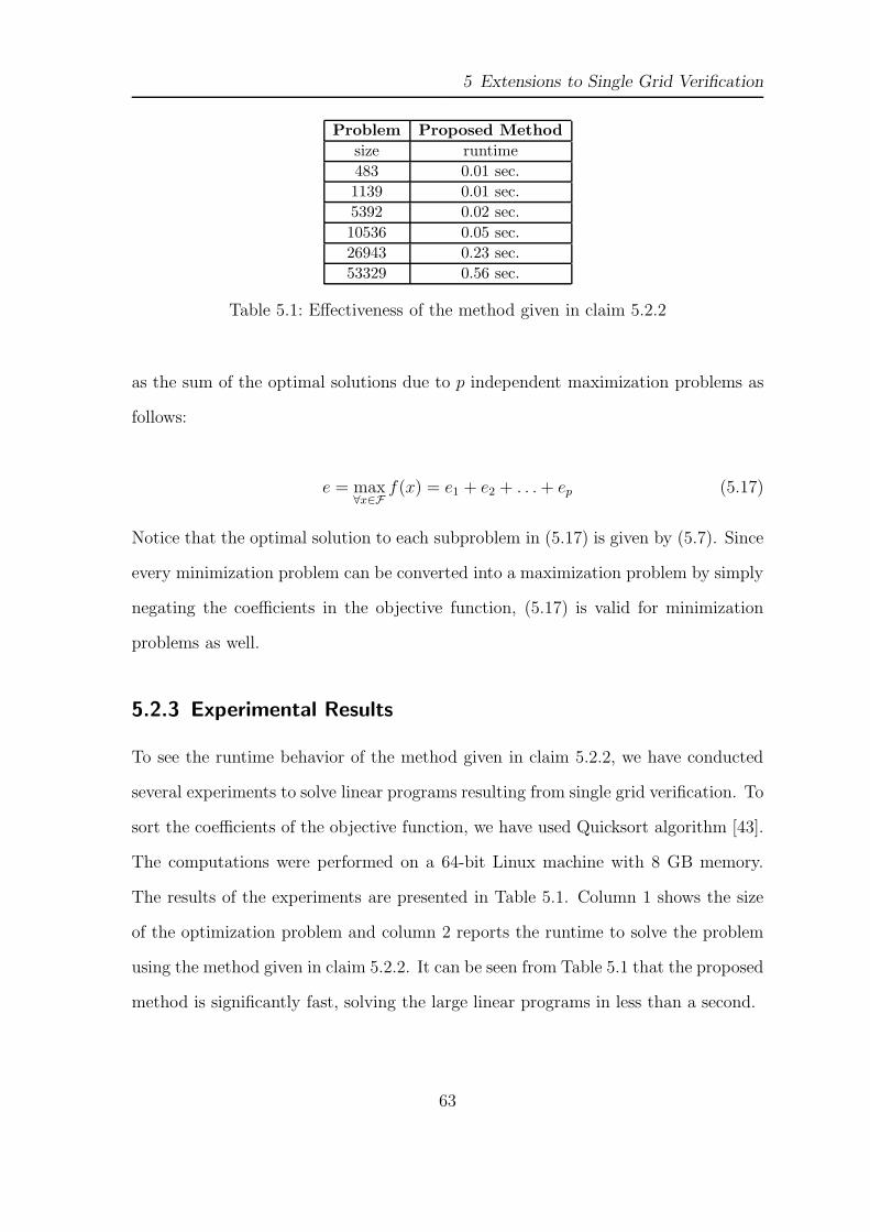
Problem Proposed Method

size runtime

483 0.01 sec.

1139 0.01 sec.

5392 0.02 sec.

10536 0.05 sec.

26943 0.23 sec.

53329 0.56 sec.

Table 5.1: Effectiveness of the method given in claim 5.2.2

as the sum of the optimal solutions due to p independent maximization problems as

follows:

e = max∀x∈F

f(x) = e1 + e2 + . . . + ep (5.17)

Notice that the optimal solution to each subproblem in (5.17) is given by (5.7). Since

every minimization problem can be converted into a maximization problem by simply

negating the coefficients in the objective function, (5.17) is valid for minimization

problems as well.

5.2.3 Experimental Results

To see the runtime behavior of the method given in claim 5.2.2, we have conducted

several experiments to solve linear programs resulting from single grid verification. To

sort the coefficients of the objective function, we have used Quicksort algorithm [43].

The computations were performed on a 64-bit Linux machine with 8 GB memory.

The results of the experiments are presented in Table 5.1. Column 1 shows the size

of the optimization problem and column 2 reports the runtime to solve the problem

using the method given in claim 5.2.2. It can be seen from Table 5.1 that the proposed

method is significantly fast, solving the large linear programs in less than a second.

63

5 Extensions to Single Grid Verification

5.3 Solution for Tree-structured Global Constraints

In [39], the authors solve a simple class of linear programs with tree-structured con-

straint matrices. The special linear programming structure is in the following form:

maximize:∑

j∈J

cjxj

subject to:∑

j∈J(i)

ajxj ≤ bi, i = 1, . . . , m

0 ≤ xj ≤ uj, j ∈ J

(5.18)

where bi, cj and aj are positive scalars, J = ∪mi=1J(i), and the sets J(i) are nested

meaning that if i 6= k, either J(i) and J(k) are disjoint, or one set is properly contained

in the other. We may assume that bi < bk, whenever J(i) is a proper subset of J(k).

When m = 1, (5.18) reduces to the fractional knapsack problem with upper bounds

on variables.

In each column of the constraint matrix, all nonzero entries are equal and positive.

This is also the case for the tree-structured linear programs in our formulation, be-

cause all nonzero entries in the global constraint matrix are 1s. The only difference

between (5.18) and the linear programs in our formulation is the lower bound for the

global constraints. However, it is shown in [44] that the results obtained in [39] are

valid for linear programs with nonnegative lower bounds for the constraint matrices.

The solution method shown in [39] separates the problem into a sequence of frac-

tional knapsack problems. Each of these fractional knapsack problems require linear

time to solve, for total solution time no worse than proportional to the number of

nonzero entries in the original constraint matrix. The optimal solution is obtained

by giving each variable their minimum value from the list obtained by solving the

sequence of fractional knapsack problems.

64

6 Future Work and Conclusion

With technology scaling, the decrease in the transistor feature size has led to the

decrease of the supply voltage. As a result, the functionality of modern ICs is becom-

ing increasingly sensitive to voltage fluctuations of the power distribution network.

Significant voltage fluctuation can cause soft errors, can lead to electromigration, and

as a result, can degrade the circuit performance. Therefore, the power distribution

network verification has become an important part of the design process.

The main difficulty in power distribution network verification is that the number

of possible input vectors is very large. Since one needs to simulate the grid for a large

number of vector sequences at each node, grid simulation is clearly not practical.

Another drawback of the grid simulation is that it does not allow the designer to

verify the grid before the complete circuit has been designed. For these reasons, we

adopt the notion of current constraints to capture the uncertainty about the circuit

behavior and currents. These constraints define upper bounds on the currents drawn

by the underlying transistor circuitry, as well as upper bounds on the sum of currents.

In this thesis, we take both power and ground grids into account. We first formulate

the grid verification problem as an optimization problem to compute the exact worst-

case voltage fluctuations at each node subject to current constraints, which is seen to

be too expensive. As an alternative, we propose a solution approach that formulates

both upper and lower bounds on the worst-case voltage fluctuations. Experimental

results show that the proposed method has errors in the range of a few mV . The

65

6 Future Work and Conclusion

power of our approach is that it finds tight upper and lower bounds on the worst-case

voltage fluctuations under all feasible current combinations. It is a unique approach

that offers this type of guarantee.

We also present extensions to the single grid verification to reduce the complexity

of the problem. These extensions are only applicable to the linear programs in the

single grid verification, because of the additional equality constraints in the dual grid

verification problem. Therefore further research is needed to extend the results for

the dual grid.

The grid model presented in this work is an RC model of the grid. Since the signal

and clock frequencies are increasing, the grid inductance contributes significantly to

the voltage fluctuation. The future work on the dual grid verification should take

the inductive effects into account. Besides, the current constraints used in this work

are DC constraints. The dual grid verification problem should also be extended and

solved under transient current constraints.

66

Appendices

67

A Matrix Equalities

In this chapter, we will prove additional claims that are useful in the context of

section 4.3.1. We start with the following claim:

Claim A.0.1. I − Dp is invertible for any integer p.

Proof. From (4.59), we know that ρ(Dp) < 1, for an integer p. We also know that

the series∑∞

q=0 Xq for a square matrix X is known to converge [25] if and only if

ρ(X) < 1, under which condition the series limit is (I − X)−1, meaning that I − Dp

is invertible for an integer p. This completes the proof.

With the help of claim A.0.1, we will prove the following claim:

Claim A.0.2. Suppose W (p) is a function of p for p ≥ 1 defined as:

W (p) = (I − Dp)−1

p−1∑

k=0

DkH (A.1)

Then W (p) = W (1), ∀p ≥ 1.

Proof. The case for p = 1 is satisfied trivially. The claim is true by induction if we

prove the following, ∀p ≥ 2:

W (p − 1) = W (1) ⇒ W (p) = W (1) (A.2)

Left multiplying both sides of (A.1) with (I −Dp), and breaking the sum∑p−1

k=0 DkH

into∑p−2

k=0 DkH and Dp−1H , we obtain:

68

A Matrix Equalities

(I − Dp)W (p) =

p−2∑

k=0

DkH + Dp−1H (A.3)

From claim A.0.1, we know that I−Dp is invertible for an integer p. Left multiplying

both sides of (A.3) with (I − Dp−1)−1, we get:

(I − Dp−1)−1(I − Dp)W (p) = (I − Dp−1)−1

p−2∑

k=0

DkH + (I − Dp−1)−1Dp−1H (A.4)

Since (I−Dp−1)−1∑p−2

k=0 DkH = W (p−1), we can replace it with W (1). Rearranging

the terms of (A.4), we have:

(I − Dp−1)−1((I − Dp)W (p) − Dp−1H

)= W (1) (A.5)

Left multiplying both sides of (A.5) with (I − Dp−1) leads to:

W (p) − DpW (p) − Dp−1 = W (1) − Dp−1W (1) (A.6)

Adding Dp−1W (1) to both sides of (A.6) and rearranging the terms, we obtain:

W (p) − W (1) = (I − Dp)−1Dp−1(H − (I − D)W (1)) (A.7)

Replacing W (1) on the left-hand side of (A.7) with (I − D)−1H leads to:

W (p) − W (1) = (I − Dp)−1Dp−1(H − H) = 0 (A.8)

Meaning that W (p) = W (1). This completes the proof.

Finally, our main result is captured in the following claim:

69

A Matrix Equalities

Claim A.0.3. For any integer p ≥ 1,

DpK = K −

p−1∑

k=0

DkH (A.9)

Proof. Since W (p) = W (1) by A.0.2, meaning that:

(I − Dp)−1

p−1∑

k=0

DkH = (I − D)−1H (A.10)

Left multiplying both sides of (A.10) with (I − Dp), we obtain:

p−1∑

k=0

DkH = (I − Dp)(I − D)−1H (A.11)

Since D = A−1B and B = A −G, we have D = A−1(A −G) = I − A−1G, leading to

I − D = A−1G. Since K and H are the matrices obtained as the first m columns of

G−1 and A−1, respectively, we can write K = (I − D)−1H , leading to:

p−1∑

k=0

DkH = (I − Dp)K (A.12)

Rearranging the terms of (A.12), we get:

K = (I − Dp)−1

p−1∑

k=0

DkH (A.13)

which completes the proof.

70

References

[1] M. Popovich, A. V. Mezhiba, and E. G. Friedman. Power distribution networkswith on-chip decoupling capacitors. Springer, New York, USA, 2008.

[2] Semiconductor Industry Association. International technology roadmap for semi-conductors, 2001.

[3] T. Chen and C. C. Chen. Efficient large-scale power grid analysis based onpreconditioned Krylov-subspace iterative methods. In ACM/IEEE Design Au-tomation Conference (DAC’01), pages 559–562, Las Vegas, NV, June 18-22 2001.

[4] M. Zhao, R. V. Panda, S. S. Sapatnekar, T. Edwards, R. Chaudhry, andD. Blaauw. Hierarchical analysis of power distribution networks. In ACM/IEEEDesign Automation Conference (DAC’00), pages 150–155, Los Angeles, CA, June5-9 2000.

[5] H. Qian and S. S. Sapatnekar. Random walks in a supply network. In ACM/IEEEDesign Automation Conference (DAC’05), pages 93–98, Anaheim, CA, June 2-62003.

[6] Semiconductor Industry Association. International technology roadmap for semi-conductors, 2009.

[7] D. Kouroussis and F. N. Najm. A static pattern-independent technique for powergrid voltage integrity verification. In ACM/IEEE Design Automation Conference(DAC’03), pages 99–104, Anaheim, CA, June 2-6 2003.

[8] M. Nizam, F. N. Najm, and A. Devgan. Power grid voltage integrity verification.In ACM/IEEE International Symposium on Low Power Electronics and Design(ISLPED’05), pages 239–244, San Diego, CA, August 8-10 2005.

[9] N. H. Abdul Ghani and F. N. Najm. Handling inductance in early power gridverification. In IEEE/ACM International Conference on Computer-Aided Design(ICCAD’06), pages 127–134, San Jose, CA, November 5-9 2006.

[10] M. Benoit, S. Taylor, D. Overhauser, and S. Rochel. Power distribution in high-performance design. In ACM/IEEE International Symposium on Low PowerElectronics and Design (ISLPED’98), pages 274–278, Monterey, CA, August 10-12 1998.

[11] L. C. Tsai. A 1 GHz PA-RISC processor. In IEEE International Solid-StateCircuits Conference, pages 322–323, San Francisco, CA, February 4-8 2001.

71

6 References

[12] C. J. Anderson, J. Petrovick, J. M. Keaty, J. Warnock, G. Nussbaum, J. M.Tendier, C. Carter, S. Chu, J. Clabes, and J. DiLullo. Physical design of afourth-generation POWER GHz microprocessor. In IEEE International Solid-State Circuits Conference, pages 232–233, San Francisco, CA, February 4-8 2001.

[13] C. Ho, A. E. Ruehli, and P. A. Brennan. The modified nodal approach to networkanalysis. IEEE Transactions on Circuits and Systems, 22(6):504–509, June 1975.

[14] J. N. Kozhaya, S. R. Nassif, and F. N. Najm. A multigrid-like technique for powergrid analysis. IEEE Transactions on Computer-Aided Design, 21(10):1148–1160,October 2002.

[15] Z. Zhu, B. Yao, and C. Cheng. Power network analysis using an adaptivealgebraic multigrid approach. In IEEE/ACM Design Automation Conference(DAC’03), pages 105–108, Anaheim, CA, June 2-6 2003.

[16] K. Wang and M. Marek-Sadowska. On-chip power supply network optimizationusing multigrid-based technique. In IEEE/ACM Design Automation Conference(DAC’03), pages 113–118, Anaheim, CA, June 2-6 2003.

[17] H. Su, E. Acar, and S. R. Nassif. Power grid reduction based on algebraicmultigrid principles. In IEEE/ACM Design Automation Conference (DAC’03),pages 109–112, Anaheim, CA, June 2-6 2003.

[18] S. R. Nassif and J. N. Kozhaya. Fast power grid simulation. In ACM/IEEE De-sign Automation Conference (DAC’00), pages 156–161, Los Angeles, CA, August2-4 2000.

[19] D. Kouroussis, I. A. Ferzli, and F. N. Najm. Incremental partitioning-basedvectorless power grid verification. In IEEE/ACM International Conference onComputer-Aided Design (ICCAD’05), pages 358–364, San Jose, CA, November6-10 2005.

[20] I. A. Ferzli, F. N. Najm, and L. Kruse. A geometric approach for early power gridverification using current constraints. In ACM/IEEE International Conferenceon Computer-Aided Design (ICCAD’07), pages 40–47, San Jose, CA, November5-8 2007.

[21] N. H. Abdul Ghani and F. N. Najm. Fast vectorless power grid verificationusing an approximate inverse technique. In ACM/IEEE Design AutomationConference (DAC’09), pages 184–189, San Francisco, CA, July 26-31 2009.

[22] M. Avci and F. N. Najm. Early p/g grid voltage integrity verification. InIEEE/ACM International Conference on Computer-Aided Design (ICCAD’10),San Jose, CA, November 7-11 2010.

[23] F. N. Najm. Circuit simulation. John Wiley & Sons, Hoboken, NJ, 2010.

72

6 References

[24] J. D. Lambert. Numerical methods for ordinary differential systems: the initialvalue problem. Jon Wiley & Sons Ltd., Chichester, UK, 1991.

[25] Y. Saad. Iterative methods for sparse linear systems. SIAM, Philadelphia, PA,2003.

[26] N. J. Higham. Accuracy and stability of numerical algorithms. SIAM, Philadel-phia, PA, 1996.

[27] N. H. Abdul Ghani and F. N. Najm. Fast vectorless power grid verification underan RLC model. Submitted to. IEEE Transactions on Computer-Aided Design ofIntegrated Circuits and Systems.

[28] S. Lang. Algebra. Addison-Wesley, Menlo Park, CA, 1993.

[29] S. Demko, W. F. Moss, and P. W. Smith. Decay rates for inverses of bandmatrices. Mathematics of Computation, 43(168):491–499, October 1984.

[30] M. J. Grote and T. Huckle. Parallel preconditioning with sparse approximateinverses. SIAM Journal on Scientific Computing, 18(3):838–853, May 1997.

[31] M. Benzi, C. D. Meyer, and M. Tuma. A sparse approximate inverse precondi-tioner for the conjugate gradient method. SIAM Journal on Scientific Comput-ing, 17(5):1135–1149, September 1996.

[32] G. H. Golub and C. F. Van Loan. Matrix computations (3rd ed.). Johns HopkinsUniversity Press, Baltimore, MD, 1996.

[33] J. Zhang. A sparse approximate inverse preconditioner for parallel precon-ditioning of general sparse matrices. Applied Mathematics and Computation,130(11):63–85, July 2002.

[34] M. Benzi and M. Tuma. A comparative study of sparse approximate inversepreconditioners. Applied Numerical Mathematics, 30(2-3):305–340, June 1999.

[35] R. K. Ahuja, T. L. Magnanti, and J. B. Orlin. Network flows: theory, algorithmsand applications. Prentice Hall, Englewood Cliffs, New Jersey, 1993.

[36] G. Sierksma. Linear and integer programming: theory and practice. MarcelDekker, New York, NY, 2001.

[37] A. Frangioni and A. Manca. A computational study of cost reoptimization formin-cost flow problems. INFORMS Journal on Computing, 18(1):61–70, 2003.

[38] Mosek: http://www.mosek.com.

[39] B. Faaland. A weighted selection algorithm for certain tree-structured linearprograms. Operations Research Journal, 32(2):405–422, March-April 1984.

73

6 References

[40] T. H. Cormen, C. E. Leiserson, R. L. Rivest, and C. Stein. Introduction ToAlgorithms. The MIT Press, Cambridge, MA, 2nd edition, 2001.

[41] R. K. Martin. Large scale linear and integer optimization: a unified approach.Kluwer Academic Publishers, Boston, MA, 1998.

[42] S. P. Bradley, A. C. Hax, and T. L. Magnanti. Applied Mathematical Program-ming. Addison-Wesley, Menlo Park, CA, 1977.

[43] C. A. R. Hoare. Quicksort. The Computer Journal, 5(1):10–16, 1962.

[44] S. S. Erenguc. An algorithm for solving a structured class of linear programmingproblems. Operations Research Letters, 4(6):293–299, April 1986.

74


Recommended