CADSOFT EAGLE 5.11 TUTORIAL By Serge Nazarenko The purpose of this tutorial is to help you to learn the basics of Eagle software. As you start using this software to make the PCB for your design project, you will find that this tutorial will save you hours of reading the software manual. You can always read the manual, but it will make more sense to you after you use this tutorial. You can download free version of Eagle software from the CadSoftusa.com website. Make sure you are using the same version as the lab’s computers, NOT NEWER. The free version of the software is fully functional with only 4x4 inch maximum board size limitation. We have the full version of the CadSoft Eagle software installed on our lab’s computers. Now we are going to start using Eagle software by creating a basic schematic diagram and PCB layout. By the end of this tutorial you’ll be able to draw the schematic diagram and make the PCB layout for your design project. Open the software by clicking on the Eagle icon (Start>All Programs>EE>Eagle Layout Editor). The Control Panel will be opened. On the top left side of the screen click File>New Project When the new folder appears, name it t01. Right click on it and select NEW –Schematic. The new schematic window will open; it’s where we are going to draw the schematic for our project.
Transcript
CADSOFT EAGLE 5.11 TUTORIAL
By Serge Nazarenko
The purpose of this tutorial is to help you to learn the basics of Eagle software.
As you start using this software to make the PCB for your design project, you will find that this tutorial will
save you hours of reading the software manual. You can always read the manual, but it will make more sense
to you after you use this tutorial.
You can download free version of Eagle software from the CadSoftusa.com website. Make sure you are using
the same version as the lab’s computers, NOT NEWER. The free version of the software is fully functional with
only 4x4 inch maximum board size limitation. We have the full version of the CadSoft Eagle software installed
on our lab’s computers.
Now we are going to start using Eagle software by creating a basic schematic diagram and PCB layout. By the
end of this tutorial you’ll be able to draw the schematic diagram and make the PCB layout for your design
project.
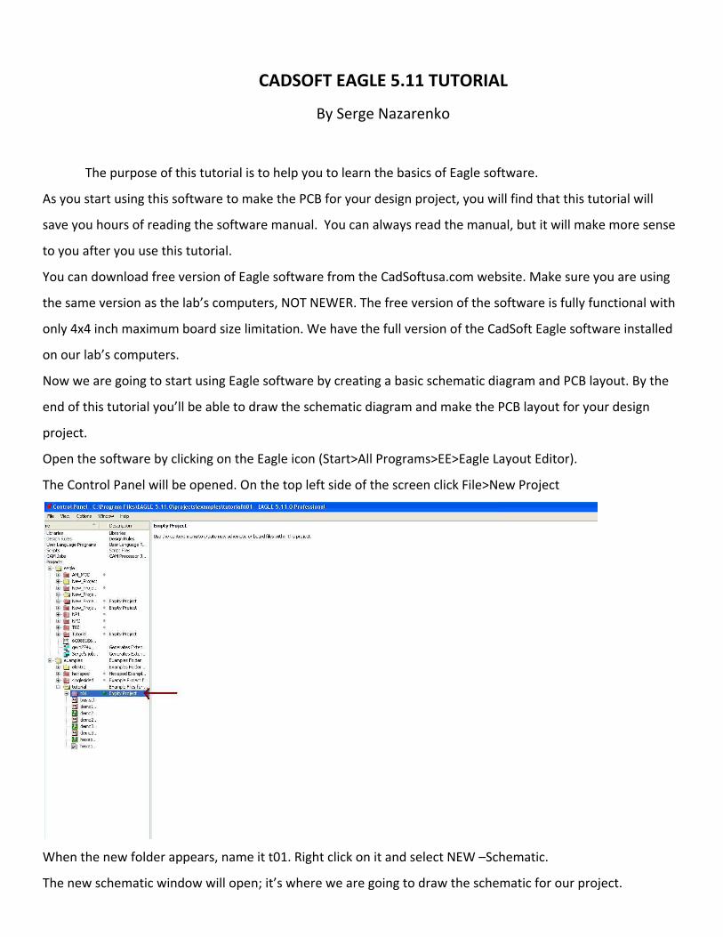
Open the software by clicking on the Eagle icon (Start>All Programs>EE>Eagle Layout Editor).
The Control Panel will be opened. On the top left side of the screen click File>New Project
When the new folder appears, name it t01. Right click on it and select NEW –Schematic.
The new schematic window will open; it’s where we are going to draw the schematic for our project.
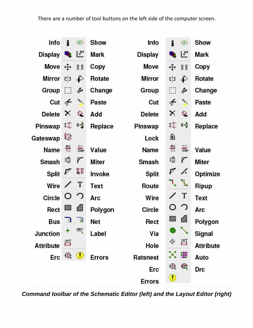
There are a number of tool buttons on the left side of the computer screen.
Command toolbar of the Schematic Editor (left) and the Layout Editor (right)
If you want to add a component to your project click on the ADD button; this will open the library.
When you scroll down to Switch and choose 320‐938, window will open. In upper right side of that window
you will see two small windows. The window on the left represents a schematic symbol of the part we chose,
and the window on the right is showing the PCB footprint of the same part.
Click the OK button and you’ll be able to move the schematic symbol of the component you chose across the
screen with the mouse.
To rotate the symbol, just right click the mouse. To place the symbol, simply move it to a desirable position
and then left click. You may place the same symbol as many times as you want. To get out just press Esc
button and Cancel, or just click on any tool icon.
The best tool would be the Move tool. You may notice that after selecting the Move tool you can move any
component by left clicking and dragging it. With this particular component, and in some other components
(especially connectors and switches), you can move sets of contacts separately in the same devise. If you want
to move the whole part use the Group tool, highlight the part, then right click and select Move: Group. Same
goes for the Mirror tool. You can mirror the whole part or just separate contacts from the same component.
To mirror the whole component select Group, Highlight the component, select mirror tool, right click on
highlighted component, and select Mirror Group. You can use the delete tool to delete your component as a
whole, by using the group tool, or by just clicking on each group of contacts.
The name tool lets you to name your component. Select the name tool, click on the component and it will
open the Name window where you can type a new name, click the ok button.
You can also use the Value tool to type the value of your component. To give you an example let’s go back to
the Library ‐RCI (where resistors capacitors and inductors are stored)‐R‐US ‐0204/7, click ok.
Select the Name tool and type R3, click ok. Select the Value tool, click on the component and type the new
value in the value window and click ok.
Let’s start with schematic diagram for the 5V power supply.
If you haven’t done it yet, delete all the components we previously placed on the schematic window.
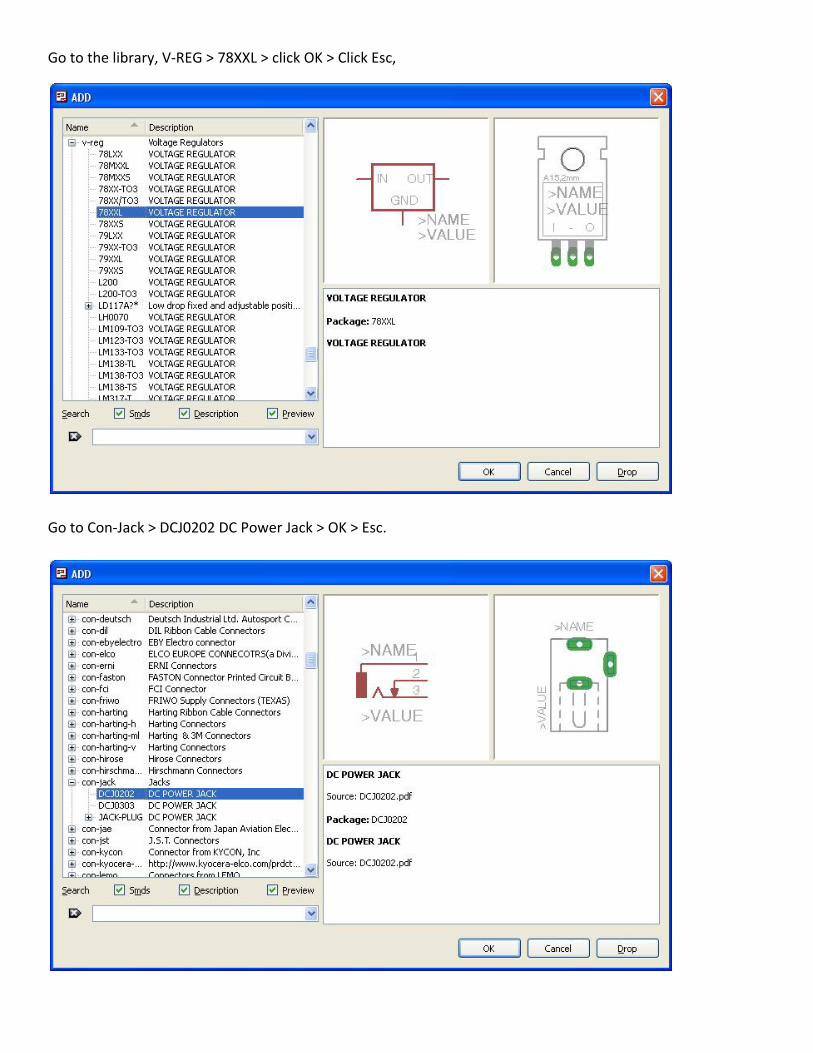
Go to the library, V‐REG > 78XXL > click OK > Click Esc,
Go to Con‐Jack > DCJ0202 DC Power Jack > OK > Esc.
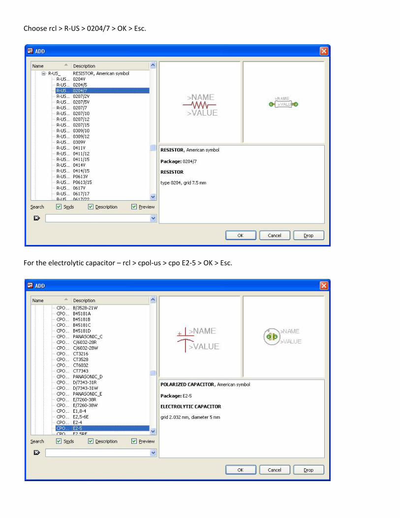
Choose rcl > R‐US > 0204/7 > OK > Esc.
For the electrolytic capacitor – rcl > cpol‐us > cpo E2‐5 > OK > Esc.
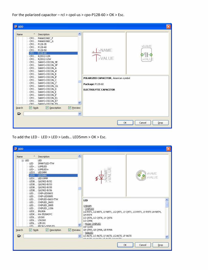
For the polarized capacitor – rcl > cpol‐us > cpo‐P128‐60 > OK > Esc.
To add the LED ‐ LED > LED > Leds… LED5mm > OK > Esc.
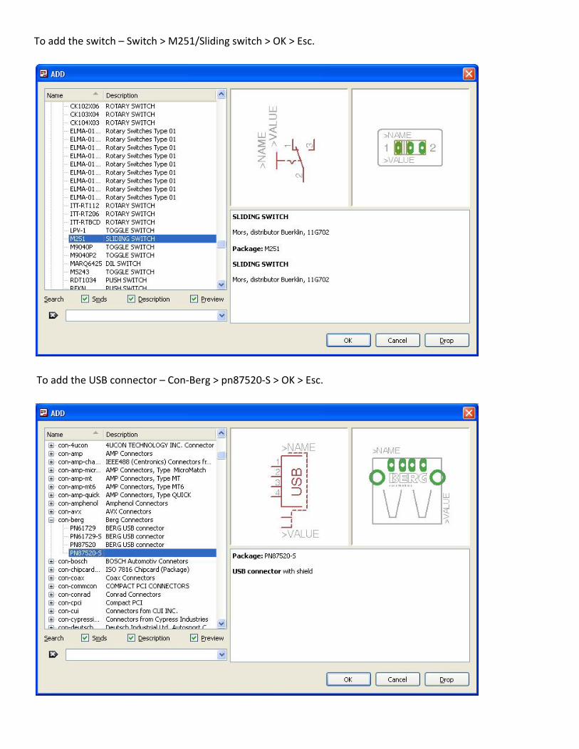
To add the switch – Switch > M251/Sliding switch > OK > Esc.
To add the USB connector – Con‐Berg > pn87520‐S > OK > Esc.
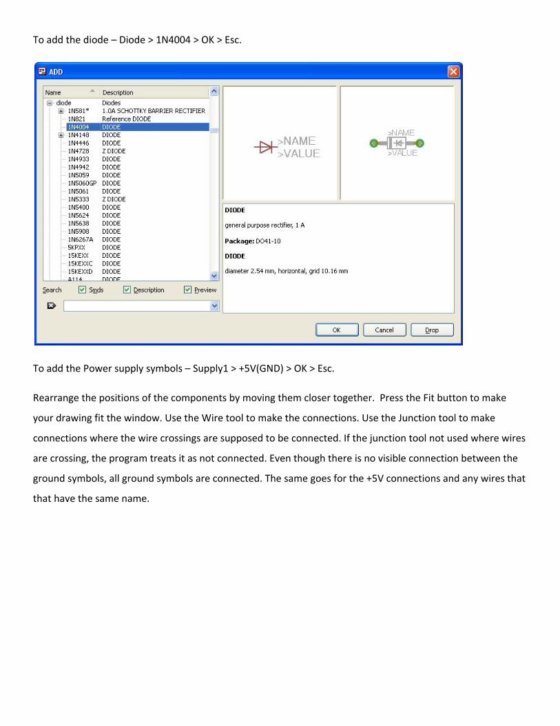
To add the diode – Diode > 1N4004 > OK > Esc.
To add the Power supply symbols – Supply1 > +5V(GND) > OK > Esc.
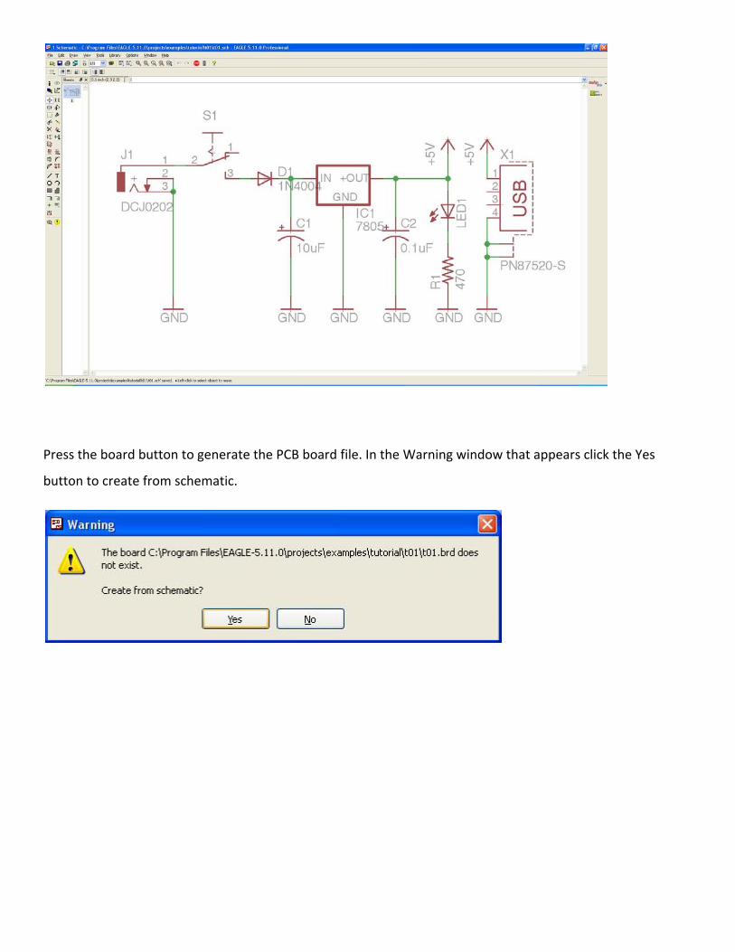
Rearrange the positions of the components by moving them closer together. Press the Fit button to make
your drawing fit the window. Use the Wire tool to make the connections. Use the Junction tool to make
connections where the wire crossings are supposed to be connected. If the junction tool not used where wires
are crossing, the program treats it as not connected. Even though there is no visible connection between the
ground symbols, all ground symbols are connected. The same goes for the +5V connections and any wires that
that have the same name.
Press the board button to generate the PCB board file. In the Warning window that appears click the Yes
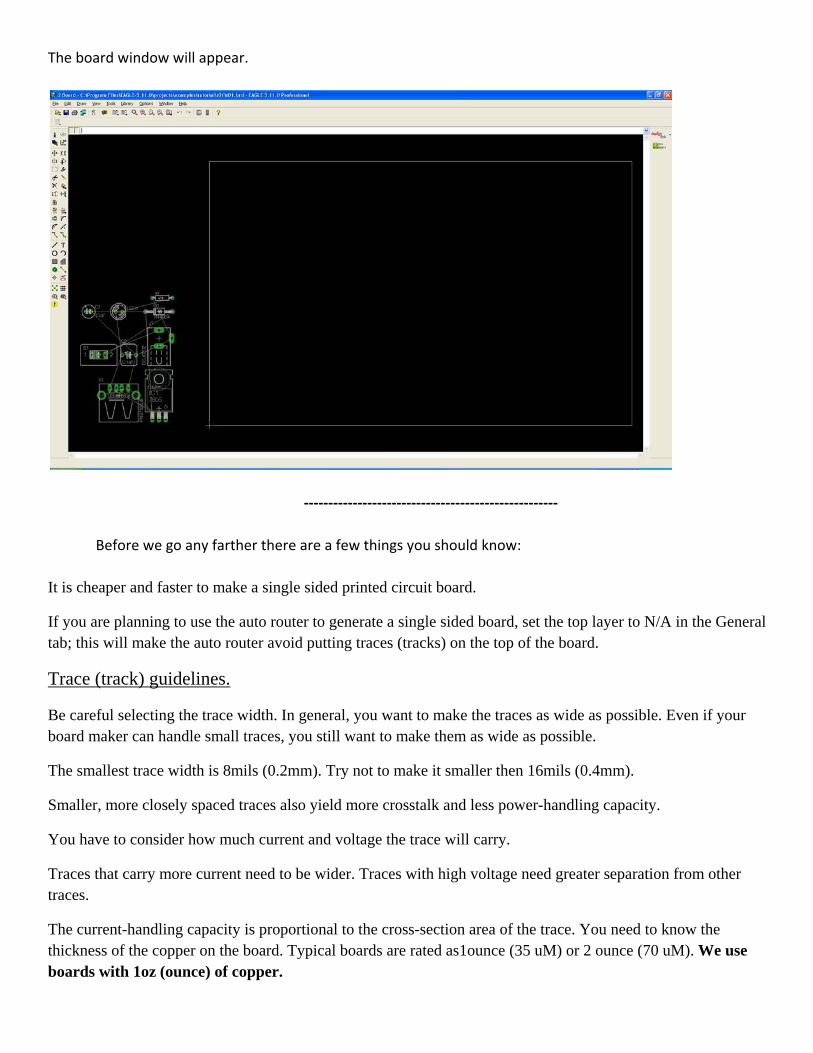
Before we go any farther there are a few things you should know:
It is cheaper and faster to make a single sided printed circuit board.
If you are planning to use the auto router to generate a single sided board, set the top layer to N/A in the General tab; this will make the auto router avoid putting traces (tracks) on the top of the board.
Trace (track) guidelines.
Be careful selecting the trace width. In general, you want to make the traces as wide as possible. Even if your board maker can handle small traces, you still want to make them as wide as possible.
The smallest trace width is 8mils (0.2mm). Try not to make it smaller then 16mils (0.4mm).
Smaller, more closely spaced traces also yield more crosstalk and less power-handling capacity.
You have to consider how much current and voltage the trace will carry.
Traces that carry more current need to be wider. Traces with high voltage need greater separation from other traces.
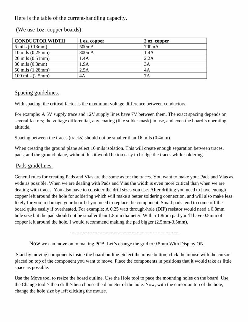
The current-handling capacity is proportional to the cross-section area of the trace. You need to know the thickness of the copper on the board. Typical boards are rated as1ounce (35 uM) or 2 ounce (70 uM). We use boards with 1oz (ounce) of copper.
Here is the table of the current-handling capacity.
With spacing, the critical factor is the maximum voltage difference between conductors.
For example: A 5V supply trace and 12V supply lines have 7V between them. The exact spacing depends on several factors; the voltage differential, any coating (like solder mask) in use, and even the board’s operating altitude.
Spacing between the traces (tracks) should not be smaller than 16 mils (0.4mm).
When creating the ground plane select 16 mils isolation. This will create enough separation between traces, pads, and the ground plane, without this it would be too easy to bridge the traces while soldering.
Pads guidelines.
General rules for creating Pads and Vias are the same as for the traces. You want to make your Pads and Vias as wide as possible. When we are dealing with Pads and Vias the width is even more critical than when we are dealing with traces. You also have to consider the drill sizes you use. After drilling you need to have enough copper left around the hole for soldering which will make a better soldering connection, and will also make less likely for you to damage your board if you need to replace the component. Small pads tend to come off the board quite easily if overheated. For example; A 0.25 watt through-hole (DIP) resistor would need a 0.8mm hole size but the pad should not be smaller than 1.8mm diameter. With a 1.8mm pad you’ll have 0.5mm of copper left around the hole. I would recommend making the pad bigger (2.5mm-3.5mm).
Now we can move on to making PCB. Let’s change the grid to 0.5mm With Display ON.
Start by moving components inside the board outline. Select the move button; click the mouse with the cursor placed on top of the component you want to move. Place the components in positions that it would take as little space as possible.
Use the Move tool to resize the board outline. Use the Hole tool to pace the mounting holes on the board. Use the Change tool > then drill >then choose the diameter of the hole. Now, with the cursor on top of the hole, change the hole size by left clicking the mouse.
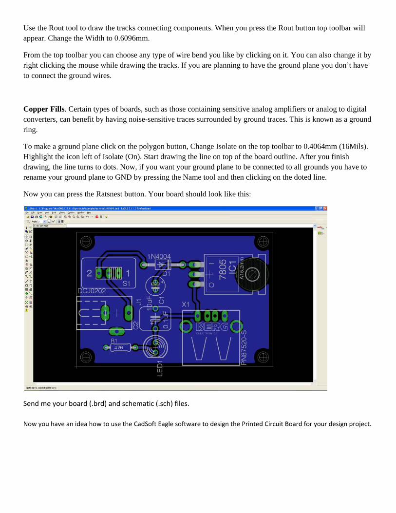
Use the Rout tool to draw the tracks connecting components. When you press the Rout button top toolbar will appear. Change the Width to 0.6096mm.
From the top toolbar you can choose any type of wire bend you like by clicking on it. You can also change it by right clicking the mouse while drawing the tracks. If you are planning to have the ground plane you don’t have to connect the ground wires.
Copper Fills. Certain types of boards, such as those containing sensitive analog amplifiers or analog to digital converters, can benefit by having noise-sensitive traces surrounded by ground traces. This is known as a ground ring.
To make a ground plane click on the polygon button, Change Isolate on the top toolbar to 0.4064mm (16Mils). Highlight the icon left of Isolate (On). Start drawing the line on top of the board outline. After you finish drawing, the line turns to dots. Now, if you want your ground plane to be connected to all grounds you have to rename your ground plane to GND by pressing the Name tool and then clicking on the doted line.
Now you can press the Ratsnest button. Your board should look like this:
Send me your board (.brd) and schematic (.sch) files.
Now you have an idea how to use the CadSoft Eagle software to design the Printed Circuit Board for your design project.
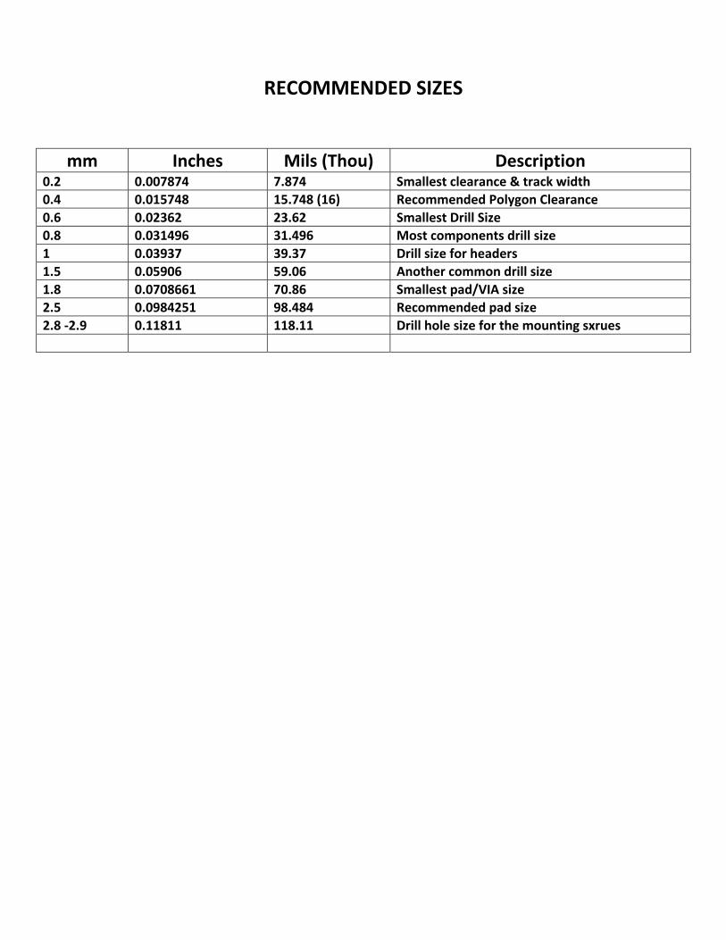
RECOMMENDED SIZES
mm Inches Mils (Thou) Description0.2 0.007874 7.874 Smallest clearance & track width 0.4 0.015748 15.748 (16) Recommended Polygon Clearance 0.6 0.02362 23.62 Smallest Drill Size 0.8 0.031496 31.496 Most components drill size 1 0.03937 39.37 Drill size for headers 1.5 0.05906 59.06 Another common drill size 1.8 0.0708661 70.86 Smallest pad/VIA size 2.5 0.0984251 98.484 Recommended pad size 2.8 ‐2.9 0.11811 118.11 Drill hole size for the mounting sxrues
ABOUT LIBRARY
The components you are adding to schematics and boards are stored in libraries. You may want to look at different
components stored in Eagle Library. The Library Editor has the same user interface as the Schematic and Layout Editor.
Therefore, you only need to know a few additional commands for defining your own components.
A library normally consists of three basic elements:
Package: The footprint in the layout
Symbol: The drawing for the schematic
Device: The real component, consisting of symbols and packages
A library also defines things like the naming conventions used, the variants available, and the exact correspondence between the logical pins of the schematic symbol and the pads on the package.
Certain exceptions don’t have these three distinct items. For example: power supply symbols (like Vcc, Vss or GND) have symbols, but no packages. Frames and other decorative “components” don’t have packages or pins. You can also make a library containing nothing but packages, which is useful when laying out boards without using schematic capture.
You can update the library from the CadSoft and component manufacture’s websites. You also can create your own library and design your own components. The easiest way to create your own component is by modifying an existing component.
We will talk about the library in more detail at the Library Tutorial.