28
AIST’s Nanotechnology .......... 4World Nanotech Projects .......... 7
Nanotechnology: A Breakthrough toward a Resource & Energy Compatible Society of the 21st Century .......... 8Carbon Nanotube Industrial Applications .......... 10
A New Type of Nanotube Formed from Molecules .......... 12The Impact of Nanotechnology in Electron Devices .......... 14
Managing Chemical Risks Using Environmental Nanotechnology .......... 16Computational Sciences on the Frontiers of Nanotechnology .......... 18
The Nanotechnology Program Projects and NEDO's Project Management .......... 20The Propagation Effect of Nanotechnology on the Economy .......... 22
The Nanoprocessing Partnership Program: AIST as Incubator for Nanotech Japan .......... 23Nanotech Ventures .......... 23
The Future of Continuously Developing Nanocarbons .......... 24AIST’s Nanotechnology Technical Development Outlook .......... 25
AIST Organization Chart .......... 26
C O N T E N T S

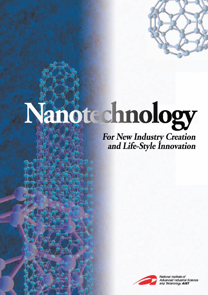
For New Industry Creation and Life-Style InnovationNanotechnology
4AIST’s Nanotechnology
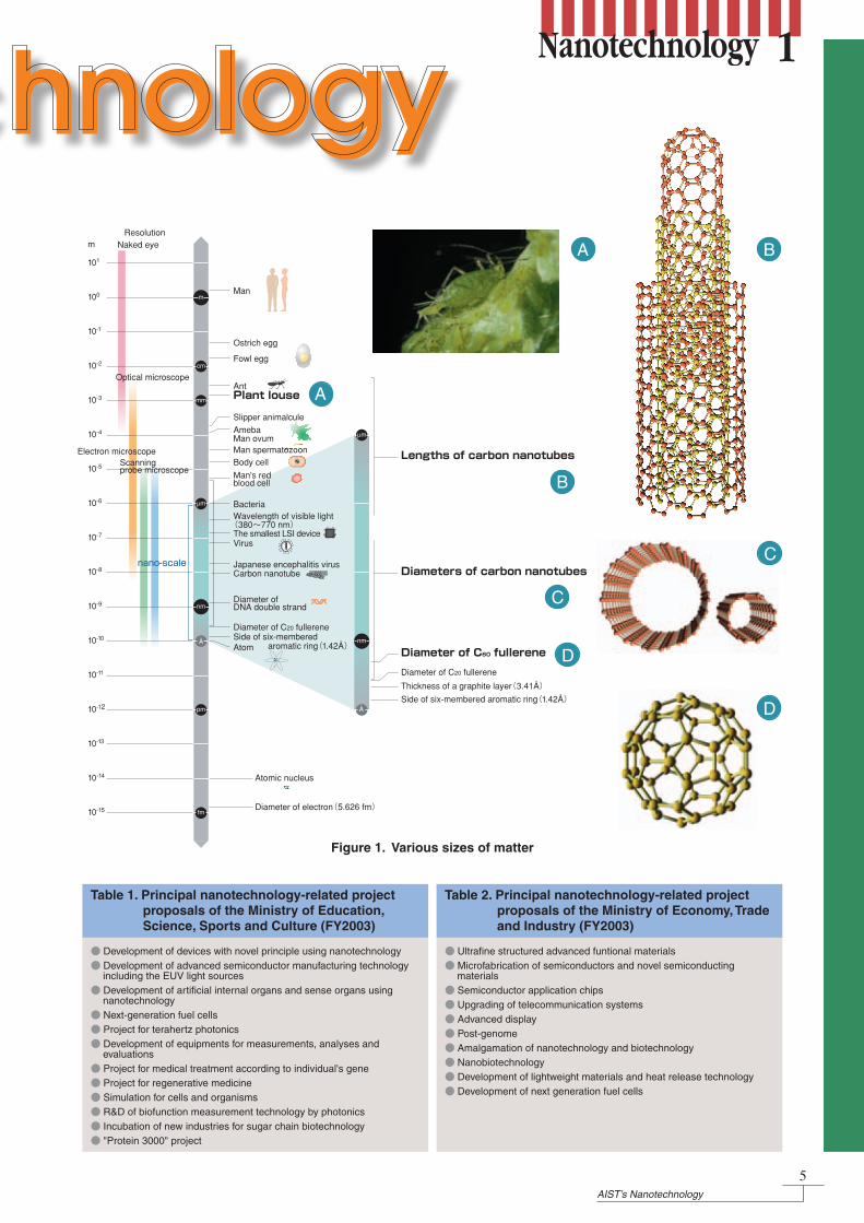
Nanotechnology is technology to manipulate and control a substance at the nanometer (nm) level (1 nm = one billionth of a meter. The nanometer level is the level of atoms and molecules. See Figure 1), and create new materials and devices with fascinating functions making the best use of the special properties of nano-sized substances. For example, today people need de-vices able to store information at high densities and high speeds, using little energy. One way of realizing this is to make each component very small. However, as there are limits to miniaturizing components with existing technology, we need technology that uses a different (nanotechnology) approach to process components and systems with nanometer-level precision. Also, when the size of the matter is at the level of several molecules or atoms, certain properties (the quantum effect or the surface effect) are clarified, which are not particularly noticeable when a substance is a large mass. Therefore, the downsizing to the nanometer level can provide us not only the miniatures but also completely new devices operated by such special properties.
The rapid development of nanotechnology research in recent years is closely related to advances made in metrology. For example, in the first half of the1980s, the IBM Group invented the scanning tunneling micro-scope, which enabled researchers to observe and ma-nipulate a substance at the level of individual atoms and molecules. This opened the wey for creating and verify-ing various nano-structures. The two methods of controlling the structure of matter at the nanometer level are the top-down and bottom-up methods. In the top-down approach, larger masses are finely processed, as in lithography, with light or electron beams. In the bottom-up approach, structures are created by assembling atoms and molecules. Vari-ous different bottom-up approaches are being studied. In addition to the munipulation of individual atoms by a scanning tunneling microscop, methods using the self-assembly of atoms and molecules (where atoms and molecules come together to form stable structures) are being researched as well as methods using the self-orga-nization of a substance (where nanoscale structures form spontaneously under certain conditions), as manifested in living organisms. Currently, there is considerable in-terest in combining top-down and bottom-up approaches to develop technologies for assembling and operating complex components and systems.
Kazuo IGARASHIResearch Coordinator [email protected]
What is Nanotechnology?
While nanotechnology is a comparatively new field of research, it has promising applications to a range of industrial fields. In the information technology area, researchers are investigating the application of nano-technology to the development of, for example, high-density/efficiency memories, computer devices with completely new operating principles, high-luminosity devices using nano-materials such as carbon nanotubes, and high-speed optical network devices using photonic crystals. In medical area, specialists are working on drug injections to certain organs using liposomes or nanoma-chines. And in the environmental and energy industries, it is thought that nanotechnology can be utilized in such applications as environment remediation catalysts and hydrogen-loading materials. In this way, nanotechnol-ogy is creating new industries across a wide range of fields and attracting interest as a infrastructural technol-ogy for enriching society.
Six government departments carry out nanotech-nology-related national projects in Japan. These are the Ministry of Education, Science, Sports and Culture (MEXT), the Ministry of Economy, Trade and Industry (METI), the Ministry of Public Management, Home Affairs, Posts and Telecommunications, the Ministry of Health, Labor and Welfare, the Ministry of Agricul-ture, Forestry and Fisheries, and the Ministry of the Environment. The total nanotechnology-related budget for FY2003 is expected to be more than the last year’s amount (¥81.6 billion). Of this amount, most was allo-cated to MEXT and METI (97.5% of the FY2001 budget for nanotechnology-related projects). Both Ministries identify electronic device- and biotech-related nanotech projects as important research areas. Against this back-ground, the nanotechnology and materials R&D promo-tion project team (NTPT) of the Council for Science and Technology Policy are trying to strengthen links with government departments and agencies for collaborative projects that would result in more efficient R&D useful for industrial advancement. Through New Research Promotion Program (in-cluding so-called CREST and ERATO projects) and Nanotechnology Support Projects, MEXT is currently funding research themes that promote nanotechnology basic research (including providing nanotechnology-related facilities and constructing nanotechnology net-works). Table 1 shows the Ministry’s principal nano-technology-related project proposals for FY2003. The
Metrology advancements have given nanotechnology a big boost
Application to industrialization
Japan’s approach to nanotechnology
5AIST’s Nanotechnology
D
C
A
B
D
C
BA
● Development of devices with novel principle using nanotechnology● Development of advanced semiconductor manufacturing technology
including the EUV light sources● Development of artificial internal organs and sense organs using
nanotechnology ● Next-generation fuel cells● Project for terahertz photonics● Development of equipments for measurements, analyses and
evaluations● Project for medical treatment according to individual's gene● Project for regenerative medicine● Simulation for cells and organisms● R&D of biofunction measurement technology by photonics● Incubation of new industries for sugar chain biotechnology● "Protein 3000" project
● Ultrafine structured advanced funtional materials● Microfabrication of semiconductors and novel semiconducting
materials● Semiconductor application chips● Upgrading of telecommunication systems● Advanced display● Post-genome● Amalgamation of nanotechnology and biotechnology● Nanobiotechnology● Development of lightweight materials and heat release technology● Development of next generation fuel cells
Table 1. Principal nanotechnology-related project proposals of the Ministry of Education, Science, Sports and Culture (FY2003)
Table 2. Principal nanotechnology-related project proposals of the Ministry of Economy, Trade and Industry (FY2003)
Figure 1. Various sizes of matter
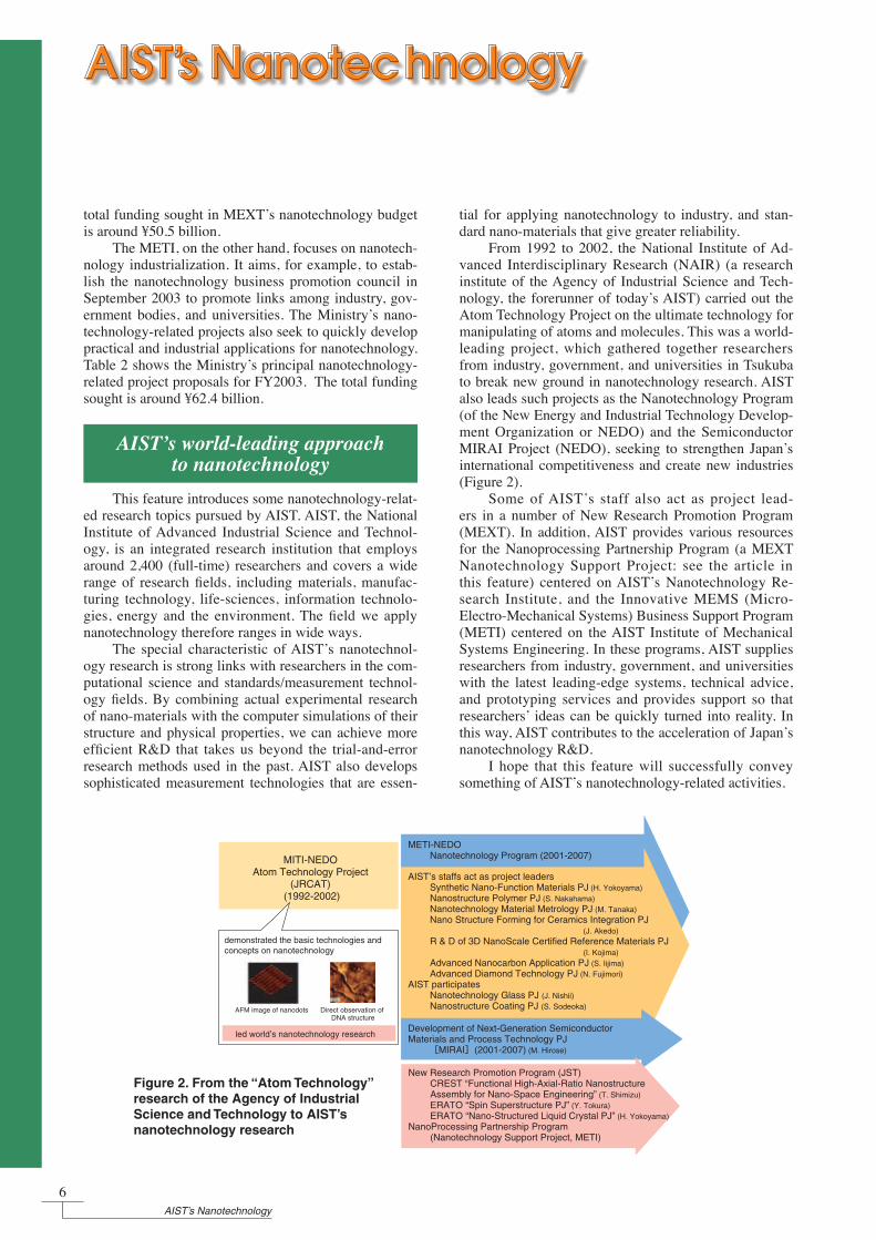
MITI-NEDOAtom Technology Project
(JRCAT) (1992-2002)
led world’s nanotechnology research
demonstrated the basic technologies and concepts on nanotechnology
AFM image of nanodots Direct observation of DNA structure
METI-NEDO Nanotechnology Program (2001-2007)
AIST’s staffs act as project leaders Synthetic Nano-Function Materials PJ (H. Yokoyama) Nanostructure Polymer PJ (S. Nakahama) Nanotechnology Material Metrology PJ (M. Tanaka) Nano Structure Forming for Ceramics Integration PJ (J. Akedo) R & D of 3D NanoScale Certified Reference Materials PJ (I. Kojima) Advanced Nanocarbon Application PJ (S. Iijima) Advanced Diamond Technology PJ (N. Fujimori)AIST participates Nanotechnology Glass PJ (J. Nishii) Nanostructure Coating PJ (S. Sodeoka)
New Research Promotion Program (JST) CREST “Functional High-Axial-Ratio Nanostructure Assembly for Nano-Space Engineering” (T. Shimizu) ERATO “Spin Superstructure PJ” (Y. Tokura) ERATO “Nano-Structured Liquid Crystal PJ” (H. Yokoyama)NanoProcessing Partnership Program (Nanotechnology Support Project, METI)
Figure 2. From the “Atom Technology” research of the Agency of Industrial Science and Technology to AIST’s nanotechnology research
total funding sought in MEXT’s nanotechnology budget is around ¥50.5 billion. The METI, on the other hand, focuses on nanotech-nology industrialization. It aims, for example, to estab-lish the nanotechnology business promotion council in September 2003 to promote links among industry, gov-ernment bodies, and universities. The Ministry’s nano-technology-related projects also seek to quickly develop practical and industrial applications for nanotechnology. Table 2 shows the Ministry’s principal nanotechnology-related project proposals for FY2003. The total funding sought is around ¥62.4 billion.
This feature introduces some nanotechnology-relat-ed research topics pursued by AIST. AIST, the National Institute of Advanced Industrial Science and Technol-ogy, is an integrated research institution that employs around 2,400 (full-time) researchers and covers a wide range of research fields, including materials, manufac-turing technology, life-sciences, information technolo-gies, energy and the environment. The field we apply nanotechnology therefore ranges in wide ways. The special characteristic of AIST’s nanotechnol-ogy research is strong links with researchers in the com-putational science and standards/measurement technol-ogy fields. By combining actual experimental research of nano-materials with the computer simulations of their structure and physical properties, we can achieve more efficient R&D that takes us beyond the trial-and-error research methods used in the past. AIST also develops sophisticated measurement technologies that are essen-
tial for applying nanotechnology to industry, and stan-dard nano-materials that give greater reliability. From 1992 to 2002, the National Institute of Ad-vanced Interdisciplinary Research (NAIR) (a research institute of the Agency of Industrial Science and Tech-nology, the forerunner of today’s AIST) carried out the Atom Technology Project on the ultimate technology for manipulating of atoms and molecules. This was a world-leading project, which gathered together researchers from industry, government, and universities in Tsukuba to break new ground in nanotechnology research. AIST also leads such projects as the Nanotechnology Program (of the New Energy and Industrial Technology Develop-ment Organization or NEDO) and the Semiconductor MIRAI Project (NEDO), seeking to strengthen Japan’s international competitiveness and create new industries (Figure 2). Some of AIST’s staff also act as project lead-ers in a number of New Research Promotion Program (MEXT). In addition, AIST provides various resources for the Nanoprocessing Partnership Program (a MEXT Nanotechnology Support Project: see the article in this feature) centered on AIST’s Nanotechnology Re-search Institute, and the Innovative MEMS (Micro-Electro-Mechanical Systems) Business Support Program (METI) centered on the AIST Institute of Mechanical Systems Engineering. In these programs, AIST supplies researchers from industry, government, and universities with the latest leading-edge systems, technical advice, and prototyping services and provides support so that researchers’ ideas can be quickly turned into reality. In this way, AIST contributes to the acceleration of Japan’s nanotechnology R&D. I hope that this feature will successfully convey something of AIST’s nanotechnology-related activities.
6AIST’s Nanotechnology
AIST’s world-leading approach to nanotechnology
AIST’s Nanotechnology
World Nanotech Projects
beginning to end to be environmentally friendly includ-ing conservation of resources and energy all the while curbing costs. European research is divided into Framework Programs implemented by the European Commission, in which joint research is done with several countries and National Programs carried out within each country. The Sixth Framework Program (2002 - 2006) is the latest of the framework programs. This program which includes eight priority areas will support industry and aims at true technological innovation in a wide range of fields from basic research to products. The total budget for the eight priority areas is 11.3 billion euros. Nanotechnology-related area, “Nanotechnologies and Nanosciences, Knowledge-based Multifunctional Ma-terials and New Production Processes and Devices,” is one of the eight priority areas, and is funded at 1.3 bil-lion euros (around US$1.8 billion), or 11.5% of the total budget. It is seen as crucially important technology for a next generation industrial revolution. In Germany, national nanotechnology-related R&D programs are actively promoted with the support of the federal government centered on the Federal Ministry of Education and Research and the Federal Ministry of Economics and Labor. A total of 18 million euros is being spent on nanocomposites and other new materials; 21 million euros on probes and other physics and chemistry areas; and 4.6 million euros on laser research, including metrology. In Switzerland, a national research plan known as “Top Nano 21” is pur-suing biotech, device, materials, and other research jointly with universities and corporations. And in the United Kingdom, nanotechnology research is sup-ported mainly through the Engineering and Physical Sciences Research Council (EPSRC) in partnership with the Department of Trade and Industry.
Trends in Korea, Taiwan, and China are attracting interest. In March 2002, Korea’s Ministry of Science and Technology (MOST) announced a plan to invest 203 billion won (US$170 million, FY2002) in the nano-technology field. In Taiwan, the government’s invest-ment in nanotechnology over the six years from 2002 is expected to total TW$23.1 billion (US$670 million). And in China, over the five years from 2001 to 2005, the central government will reportedly invest 2 billion yuan (US$240 million) in the field, while provincial gov-ernments will spend 2 – 3 billion yuan (US$240-360 million) on nanotechnology over the same period.
In the United States, the first country in the world which started nanotechnology-related national-scale project known as the National Nanotechnology Ini-tiative (NNI), nanotechnology, that is nanoscale sci-ence and technology, is recognized to be not simply a field of understanding of materials and phenomena or development of technology but an intersectional, general and fundamental concept concerned with vari-ous industrial and social fields such as materials and manufacturing, electronics and computer technology, medicine and health, aeronautics and space explora-tion, environment and energy, biotechnology and ag-riculture, and national security. It is regarded as a key driver to have influence on future industrial competi-tiveness of developed countries. It is also recognized to have a strong character of new field-fusion science. Its implementation content is very general and widely embracing and includes education and training as well as research and development. Funding is allocated to such areas as long-term basic research, Grand Chal-lenges, interdisciplinary nanotechnology research cen-ter, research infrastructure and equipment, technology transfer, education and training. The NNI is managed by the Committee on Tech-nology (CT) of the National Science and Technology Council (NSTC). The Nanoscale Science, Engineering and Technology (NSET), the CT’s subcommittee, co-ordinates many US federal nanoscale R&D programs including the NNI, and plans, drafts and implements the NNI. The total NNI budget is steadily increasing: US$464 million (FY2001), US$604 million (FY2002), US$774 million$ (FY2003), US$847 million (FY2004, request). While ten government departments and agencies par-ticipate in the NNI, a large portion of the budget is dis-tributed to the National Science Foundation (NSF), the Department of Defense (DOD), and the Department of Energy (DOE). These three government bodies con-sume 80% of the total NNI budget. Recently, the nanotechnology bill was submitted in both the House of Representatives and the Senate. In May, the Nanotechnology Research and Development Act was passed by the House of Representatives, and a total budget of US-2.36 billion$ has been approved for the three years starting from FY2004.
Nanotechnology in Europe includes nanotechnol-ogy and product production technology planned from
Yoshinao OOSAWA, Mami SAKASHITA, and Hirofumi OGAWATechnology Information Department
7AIST’s Nanotechnology
United States
Europe
Asia
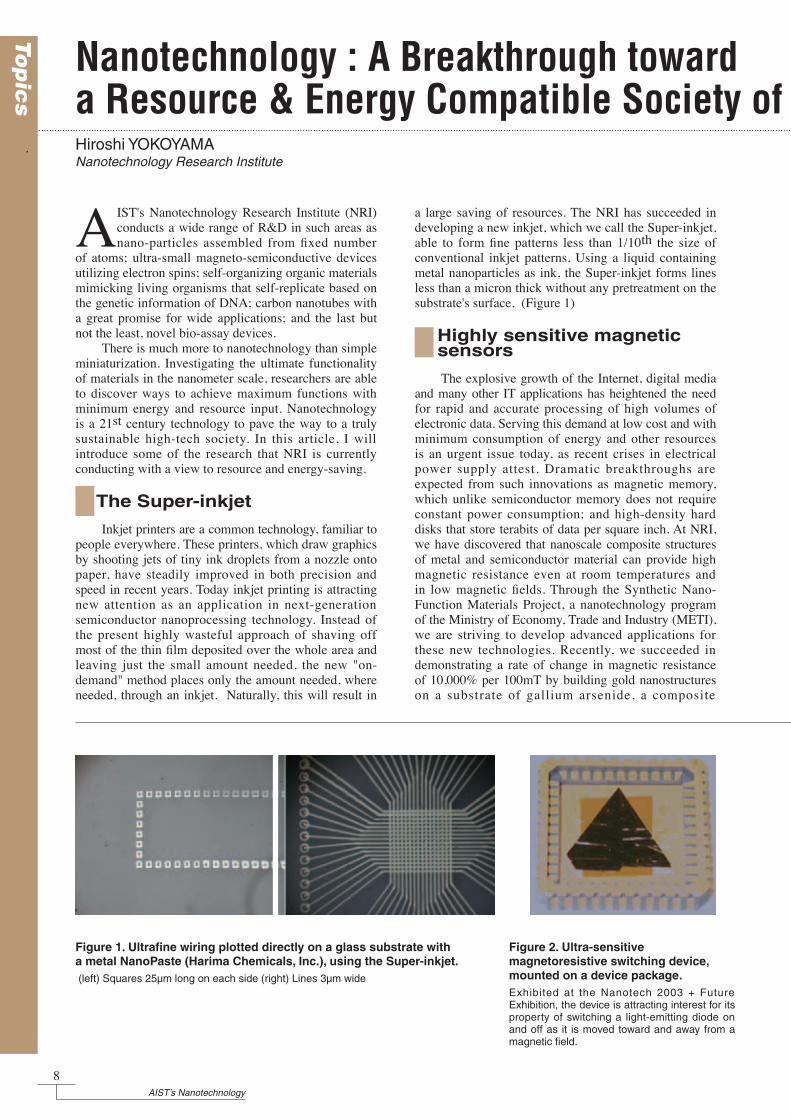
Figure 1. Ultrafine wiring plotted directly on a glass substrate with a metal NanoPaste (Harima Chemicals, Inc.), using the Super-inkjet. (left) Squares 25µm long on each side (right) Lines 3µm wide
Figure 2. Ultra-sensitive magnetoresistive switching device, mounted on a device package.Exhibited at the Nanotech 2003 + Future Exhibition, the device is attracting interest for its property of switching a light-emitting diode on and off as it is moved toward and away from a magnetic field.
8AIST’s Nanotechnology
IST's Nanotechnology Research Institute (NRI) conducts a wide range of R&D in such areas as nano-particles assembled from fixed number
of atoms; ultra-small magneto-semiconductive devices utilizing electron spins; self-organizing organic materials mimicking living organisms that self-replicate based on the genetic information of DNA; carbon nanotubes with a great promise for wide applications; and the last but not the least, novel bio-assay devices. There is much more to nanotechnology than simple miniaturization. Investigating the ultimate functionality of materials in the nanometer scale, researchers are able to discover ways to achieve maximum functions with minimum energy and resource input. Nanotechnology is a 21st century technology to pave the way to a truly sustainable high-tech society. In this article, I will introduce some of the research that NRI is currently conducting with a view to resource and energy-saving.
The Super-inkjet
Inkjet printers are a common technology, familiar to people everywhere. These printers, which draw graphics by shooting jets of tiny ink droplets from a nozzle onto paper, have steadily improved in both precision and speed in recent years. Today inkjet printing is attracting new attention as an application in next-generation semiconductor nanoprocessing technology. Instead of the present highly wasteful approach of shaving off most of the thin film deposited over the whole area and leaving just the small amount needed, the new "on-demand" method places only the amount needed, where needed, through an inkjet. Naturally, this will result in
a large saving of resources. The NRI has succeeded in developing a new inkjet, which we call the Super-inkjet, able to form fine patterns less than 1/10th the size of conventional inkjet patterns. Using a liquid containing metal nanoparticles as ink, the Super-inkjet forms lines less than a micron thick without any pretreatment on the substrate's surface. (Figure 1)
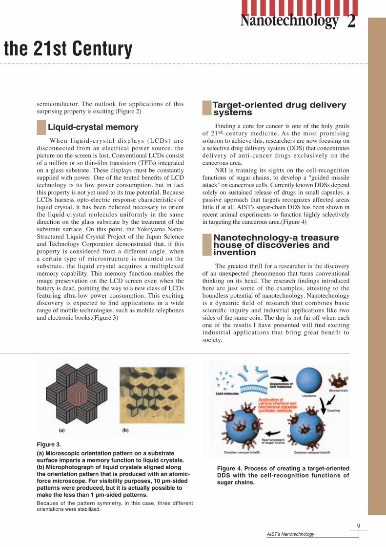
Highly sensitive magnetic sensors
The explosive growth of the Internet, digital media and many other IT applications has heightened the need for rapid and accurate processing of high volumes of electronic data. Serving this demand at low cost and with minimum consumption of energy and other resources is an urgent issue today, as recent crises in electrical power supply attest. Dramatic breakthroughs are expected from such innovations as magnetic memory, which unlike semiconductor memory does not require constant power consumption; and high-density hard disks that store terabits of data per square inch. At NRI, we have discovered that nanoscale composite structures of metal and semiconductor material can provide high magnetic resistance even at room temperatures and in low magnetic fields. Through the Synthetic Nano-Function Materials Project, a nanotechnology program of the Ministry of Economy, Trade and Industry (METI), we are striving to develop advanced applications for these new technologies. Recently, we succeeded in demonstrating a rate of change in magnetic resistance of 10,000% per 100mT by building gold nanostructures on a substrate of gallium arsenide, a composite
Hiroshi YOKOYAMANanotechnology Research Institute
Nanotechnology : A Breakthrough toward a Resource & Energy Compatible Society of the 21st Century
Top
ics
A
Nanotechnology : A Breakthrough toward a Resource & Energy Compatible Society of the 21st Century
Figure 3.
(a) Microscopic orientation pattern on a substrate surface imparts a memory function to liquid crystals. (b) Microphotograph of liquid crystals aligned along the orientation pattern that is produced with an atomic-force microscope. For visibility purposes, 10 µm-sided patterns were produced, but it is actually possible to make the less than 1 µm-sided patterns.Because of the pattern symmetry, in this case, three different orientations were stabilized.
Figure 4. Process of creating a target-oriented DDS with the cell-recognition functions of sugar chains.
9AIST’s Nanotechnology
semiconductor. The outlook for applications of this surprising property is exciting.(Figure 2)
Liquid-crystal memory
When l iquid-crys ta l d isp lays (LCDs) are disconnected from an electrical power source, the picture on the screen is lost. Conventional LCDs consist of a million or so thin-film transistors (TFTs) integrated on a glass substrate. These displays must be constantly supplied with power. One of the touted benefits of LCD technology is its low power consumption, but in fact this property is not yet used to its true potential. Because LCDs harness opto-electric response characteristics of liquid crystal, it has been believed necessary to orient the liquid-crystal molecules uniformly in the same direction on the glass substrate by the treatment of the substrate surface. On this point, the Yokoyama Nano-Structured Liquid Crystal Project of the Japan Science and Technology Corporation demonstrated that, if this property is considered from a different angle, when a certain type of microstructure is mounted on the substrate, the liquid crystal acquires a multiplexed memory capability. This memory function enables the image preservation on the LCD screen even when the battery is dead, pointing the way to a new class of LCDs featuring ultra-low power consumption. This exciting discovery is expected to find applications in a wide range of mobile technologies, such as mobile telephones and electronic books.(Figure 3)
Target-oriented drug delivery systems
Finding a cure for cancer is one of the holy grails of 21st-century medicine. As the most promising solution to achieve this, researchers are now focusing on a selective drug delivery system (DDS) that concentrates delivery of anti-cancer drugs exclusively on the cancerous area. NRI is training its sights on the cell-recognition functions of sugar chains, to develop a "guided missile attack" on cancerous cells. Currently known DDSs depend solely on sustained release of drugs in small capsules, a passive approach that targets recognizes affected areas little if at all. AIST's sugar-chain DDS has been shown in recent animal experiments to function highly selectively in targeting the cancerous area.(Figure 4)
Nanotechnology-a treasure house of discoveries and invention
The greatest thrill for a researcher is the discovery of an unexpected phenomenon that turns conventional thinking on its head. The research findings introduced here are just some of the examples, attesting to the boundless potential of nanotechnology. Nanotechnology is a dynamic field of research that combines basic scientific inquiry and industrial applications like two sides of the same coin. The day is not far off when each one of the results I have presented will find exciting industrial applications that bring great benefit to society.

10AIST’s Nanotechnology
Device (Fujitsu, NEC, AIST)
! 構造制御・量産技術Structure Control and Mass Production
Application to fuel cells (NEC)
Control of chemical functions (Mitsubishi Rayon, Chiba Univ, Nagasaki Univ, Yamagata Univ, NEC, GSI Creos, NOK, AIST)
" 物理・化学的機能制御技術Control of physical and chemical functions
Structure control
# 電気的機能制御技術Control of electric functions
・Development of analytic technology of nanocarbons (AIST)$ 構造評価技術Structural analyses
Growth control (Fujitsu, NEC, AIST)
・Fluidized bed reactor (Mitsubishi Heavy Ind.)
・Floating catalyst reactor (Nikkiso)
・CO2 laser method (NEC)
・Spinning method (TORAY)
Mass production・Catalyst development (AIST, Kyushu Univ)・Investigation on growth mechanism (IRI) ・SiC decomposition method (JFCC)
Figure 4 . Or iented mul t i -wa l l nanotubes grown perpendicularly to the substrate.
Figure 1. Nanocarbon Technology Project.
arbon nanotubes and other nanocarbons have electrical conductivity, thermal conductivity, and mechanical strength that conventional materials
cannot match. With the diversity of their structure, these characteristic values can be achieved over an extremely wide range of conditions. Nanocarbons can be used in a wide range of fields, including chemical, electrical, and mechanical, and offer great promise in the 21st century as a basic material at the core of materials nanotechnol-ogy. The Research Center for Advanced Carbon Materi-als develops the superior characteristics of nanocarbons and links them to the creation of innovative products in a wide range of industrial fields, including IT, the envi-ronment, and biotech in an effort to help reinforce the competitiveness of Japanese industry.
Nanocarbon Technology Project
The Nanocarbon Technology Project is a five-year plan running until FY2006 and involving eight corpora-tions, one association, and four universities as well as AIST (Figure 1). The project was started in October 2002 with the aim of advancing nanotube mass produc-tion technology and a broad range of applied research. From FY2003, it was reconstituted as one of the Focus 21 projects to invigorate economy. Two priority devel-opment themes, development of miniature, lightweight, and long-life mobile-type fuel cells using nanotubes as their electrodes, and electron device application technol-ogy using nanocarbon materials in semiconductor chip wiring, are receiving accelerated development. The Research Center for Advanced Carbon Materi-als is involved in all Nanocarbon Technology Project re-search themes and is pursuing this research vigorously.
Development of catalysts for mass production
In the mass production of nanotubes, the catalyst holds the key. The Research Center for Advanced Car-bon Materials has developed two types of catalysts. One is a nanometer-size metal particle catalyst (Figure 2). This is a new type of catalyst with many advantages: al-though nano-size, it can be made from a diverse range of metals, and can combine different metals. In the Nano-carbon Technology Project, this catalyst is being used in the gaseous phase reaction process under development by Nikkiso Co., Ltd. The other catalyst is based on the use of a catalyst carrier for supporting stably the 1-nm nano-particles. In the Nanocarbon Technology Project, this catalyst is being used in the fluidized bed method under development by Mitsubishi Heavy Industries, Ltd. By the admixture of the so produced nanotubes with plastics, the mechanical strength and electrical and thermal conductivity of the material are improved. The development of applications of nanotubes as new cata-lyst materials, optical materials, and gas storage materi-als is in full swing.
Ultra-high sensitivity electron microscope
The success of the above nanocarbon technologies is underpinned by the development of an ultra-high sen-sitivity, high-resolution electron microscope, which has sub-nanoscale accuracy and is able to obtain information on the atomic arrangement, element identification, and electronic structure of nanocarbon materials. Our micro-scope, the sub-nanometer structure analysis system (Fig-ure 3), is being improved, so that we have succeeded in
Motoo YUMURAResearch Center for Advanced Carbon Materials
Carbon Nanotube Industrial Applications
1
1-1
1-2
Figure 2. (left) Metal nanoparticle catalyst developed at the Center and (right) single-wall nanotubes synthesized using the catalyst.
Top
ics
C

11AIST’s Nanotechnology
nanoprobe(<0.2 nm)
Highly resolved image
Spectrometer
Information onelectronic state
1160 1180 1200 1220 1240
Counts (arb. units)
Energy loss (eV)
Gd M5
Gd M4
b Gd3+
Gd@C82
Ultrahigh sensitive elemental analysisusing ultrasmall electron probe
AIST-HD2000UHV
sample
S M
Figure 5. Towards the calculation with a carbon nanotube device.(upper) Specimen of a carbon nanotube device (S: semiconductor nanotube, M: metall ic nanotube). (lower) Nanotube grown on a catalyst pattern fabricated with lithography (a single-wall nanotube crosses over the catalyst patters)
S M
Figure 3. Sub-nanometer structure analysis system developed in the Center.
revealing individual atoms on a nanocarbon.
Further development of carbon nanotube applications From bulk use to using single nanotube characteristics
As research into nanotubes advances, research is shifting from methods of utilizing bulk nanotubes (in composite resins and FEDs, for example) to utilization of individual nanotube characteristics by combining with nano-processing technologies.
Application to electronics
The application of nanocarbon technologies to new transistors that surpass conventional silicon-based semi-conductors holds great promise. The Center is carrying out research for realizing nanotube devices, utilizing our so far developed technology on catalyst and nanotube syntheses. By the reaction of nanometer-size catalyst with acetylene on a silicon substrate, the Center has suc-ceeded in the fabrication of oriented nanotube film that grow vertically on a substrate, as in Figure 4. One prom-ising application of these oriented films is as electron sources of field emission-type devices. To extend this technology further to the develop-ment of nanotube devices, the Center has been working on developing technologies for more precise growth of nanocarbons. The Center has demonstrated that, by mix-ing catalysts with resist and forming catalyst patterns by lithography, it is able to selectively grow nanotubes (Figure 5). Through the development of micro-array technology using such catalyst reactions, the Center has opened the way to array nanotubes in lattice patterns on
substrates for ultrafine non-volatile memories and field effect transistors.
Biotech applications
Nanocarbon tubes are 100% carbon and are com-patible with cells and other organic matter. In addition, precision growth and position-direction control technol-ogies developed for nanotube electronic device applica-tions have potential for application in a number of areas in the biotech field. For example, nanotubes have proved excellent characteristics as the probes of scanning probe micro-scopes (SPM), and application to cell manipulation technology looks very promising. Nanotubes can also be chemically modified and various molecules can be joined to give them DNA separation and protein recog-nition functions. In addition, expectations are also cen-tering on such areas as the development of drug delivery systems that use nanotubes’ interior space.
Toward further development
Still further development can be achieved by merg-ing the carbon nanotube and other nanocarbon fabrica-tion and processing technologies of the Research Center for Advanced Carbon Materials with the nano-material processing and cell processing technologies of other AIST research units. AIST hopes it can create large-scale nanocarbon business centers within AIST to help strengthen the competitiveness of Japanese industry.
2
2-1
2-2
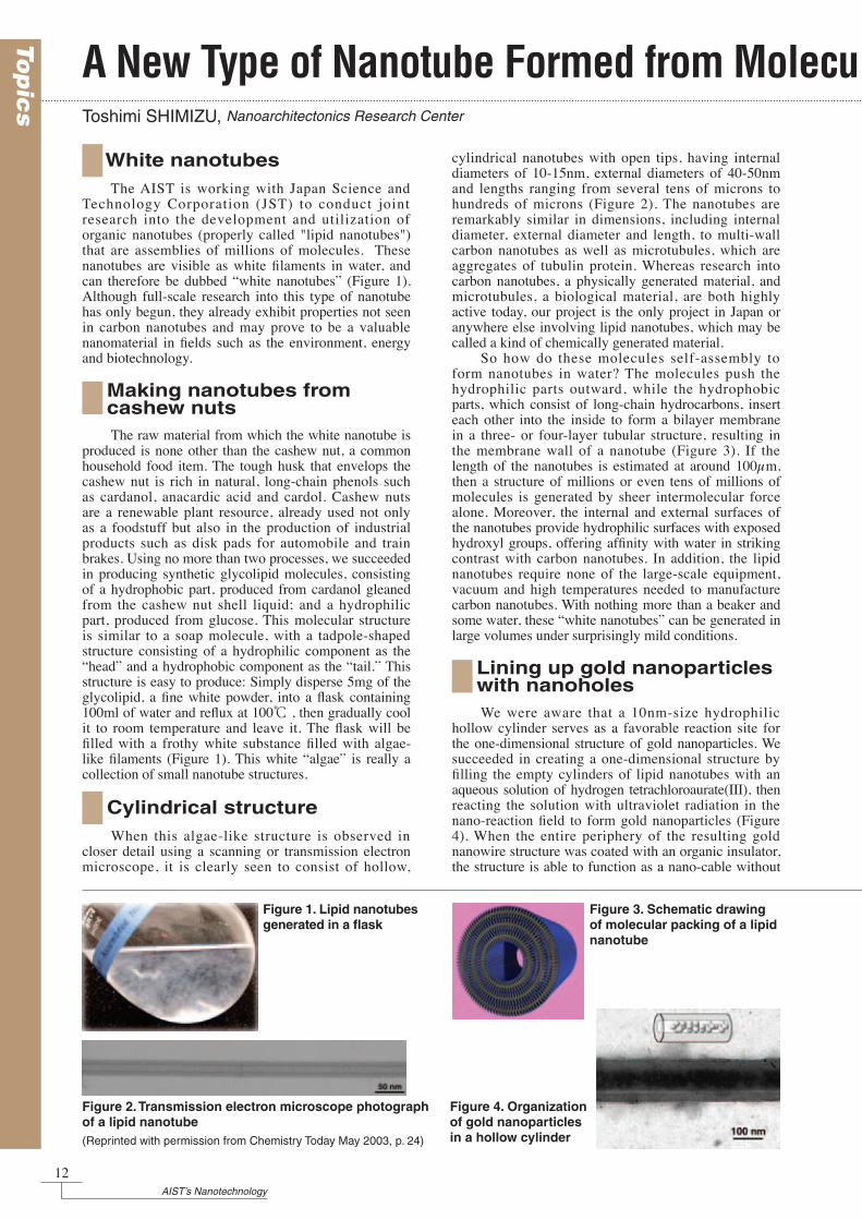
Figure 2. Transmission electron microscope photograph of a lipid nanotube(Reprinted with permission from Chemistry Today May 2003, p. 24)
Figure 1. Lipid nanotubes generated in a flask
Figure 3. Schematic drawing of molecular packing of a lipid nanotube
Figure 4. Organization of gold nanoparticles in a hollow cylinder
12AIST’s Nanotechnology
White nanotubes The AIST is working with Japan Science and Technology Corporation (JST) to conduct joint research into the development and utilization of organic nanotubes (properly called "lipid nanotubes") that are assemblies of millions of molecules. These nanotubes are visible as white filaments in water, and can therefore be dubbed “white nanotubes” (Figure 1). Although full-scale research into this type of nanotube has only begun, they already exhibit properties not seen in carbon nanotubes and may prove to be a valuable nanomaterial in fields such as the environment, energy and biotechnology.
Making nanotubes from cashew nuts The raw material from which the white nanotube is produced is none other than the cashew nut, a common household food item. The tough husk that envelops the cashew nut is rich in natural, long-chain phenols such as cardanol, anacardic acid and cardol. Cashew nuts are a renewable plant resource, already used not only as a foodstuff but also in the production of industrial products such as disk pads for automobile and train brakes. Using no more than two processes, we succeeded in producing synthetic glycolipid molecules, consisting of a hydrophobic part, produced from cardanol gleaned from the cashew nut shell liquid; and a hydrophilic part, produced from glucose. This molecular structure is similar to a soap molecule, with a tadpole-shaped structure consisting of a hydrophilic component as the “head” and a hydrophobic component as the “tail.” This structure is easy to produce: Simply disperse 5mg of the glycolipid, a fine white powder, into a flask containing 100ml of water and reflux at 100℃ , then gradually cool it to room temperature and leave it. The flask will be filled with a frothy white substance filled with algae-like filaments (Figure 1). This white “algae” is really a collection of small nanotube structures.
Cylindrical structure When this algae-like structure is observed in closer detail using a scanning or transmission electron microscope, it is clearly seen to consist of hollow,
cylindrical nanotubes with open tips, having internal diameters of 10-15nm, external diameters of 40-50nm and lengths ranging from several tens of microns to hundreds of microns (Figure 2). The nanotubes are remarkably similar in dimensions, including internal diameter, external diameter and length, to multi-wall carbon nanotubes as well as microtubules, which are aggregates of tubulin protein. Whereas research into carbon nanotubes, a physically generated material, and microtubules, a biological material, are both highly active today, our project is the only project in Japan or anywhere else involving lipid nanotubes, which may be called a kind of chemically generated material. So how do these molecules self-assembly to form nanotubes in water? The molecules push the hydrophilic parts outward, while the hydrophobic parts, which consist of long-chain hydrocarbons, insert each other into the inside to form a bilayer membrane in a three- or four-layer tubular structure, resulting in the membrane wall of a nanotube (Figure 3). If the length of the nanotubes is estimated at around 100µm, then a structure of millions or even tens of millions of molecules is generated by sheer intermolecular force alone. Moreover, the internal and external surfaces of the nanotubes provide hydrophilic surfaces with exposed hydroxyl groups, offering affinity with water in striking contrast with carbon nanotubes. In addition, the lipid nanotubes require none of the large-scale equipment, vacuum and high temperatures needed to manufacture carbon nanotubes. With nothing more than a beaker and some water, these “white nanotubes” can be generated in large volumes under surprisingly mild conditions.
Lining up gold nanoparticles with nanoholes We were aware that a 10nm-size hydrophilic hollow cylinder serves as a favorable reaction site for the one-dimensional structure of gold nanoparticles. We succeeded in creating a one-dimensional structure by filling the empty cylinders of lipid nanotubes with an aqueous solution of hydrogen tetrachloroaurate(III), then reacting the solution with ultraviolet radiation in the nano-reaction field to form gold nanoparticles (Figure 4). When the entire periphery of the resulting gold nanowire structure was coated with an organic insulator, the structure is able to function as a nano-cable without
Toshimi SHIMIZU, Nanoarchitectonics Research Center
A New Type of Nanotube Formed from Molecu les
Top
ics
Single nanotubeGlass capillary Single nanotube 0.37 mm
Lipid nanotube
0.14 mm
Glass substrate
Figure 5. Microinjection of lipid nanotubes(Reprinted with permission from Chemistry Today May 2003, p. 28)
Figure 6. Letters and frame written with lipid nanotubes(Reprinted with permission from Chemistry Today May 2003, p. 24)
13AIST’s Nanotechnology
A New Type of Nanotube Formed from Molecu les
further modification. This discovery has exciting implications, as it represents a new one-dimensional nanostructural material that can produce wires under gentle conditions beyond the limit of nanolithography (50nm).
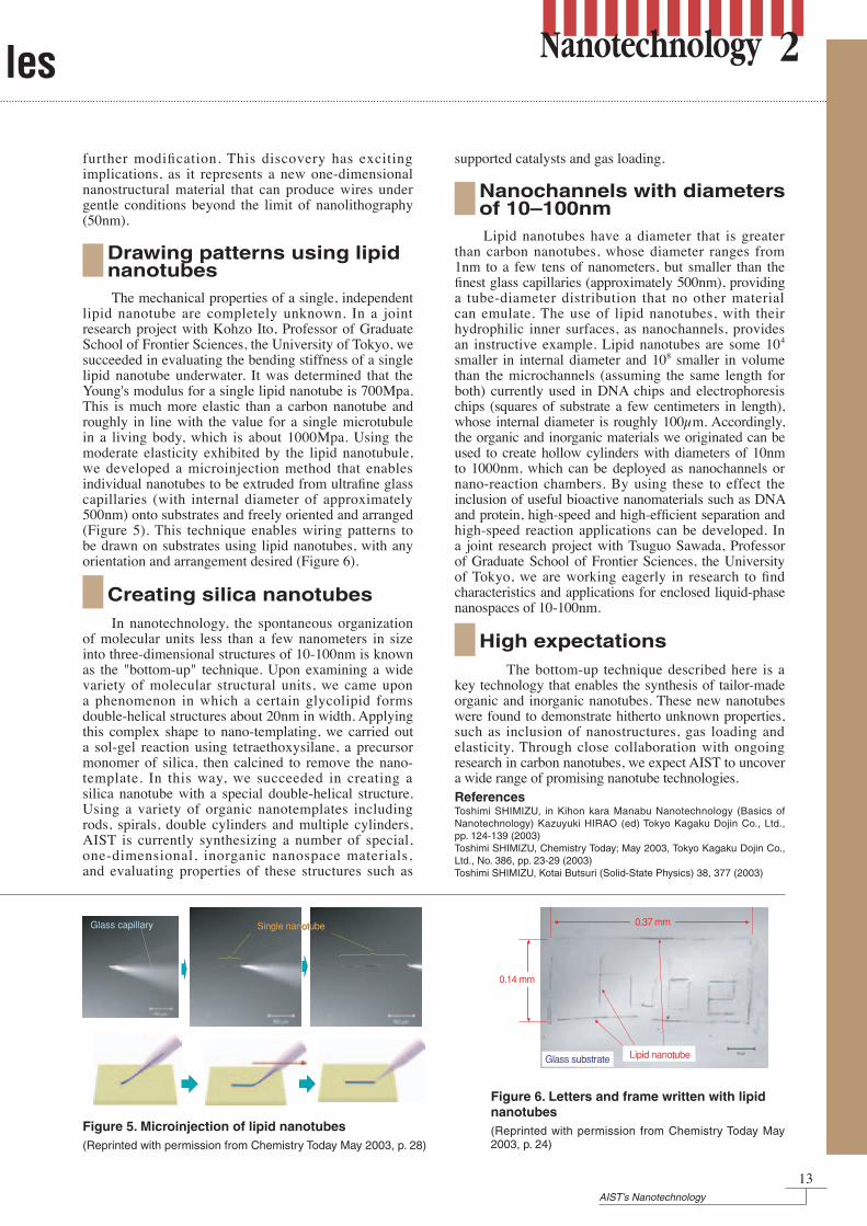
Drawing patterns using lipid nanotubes The mechanical properties of a single, independent lipid nanotube are completely unknown. In a joint research project with Kohzo Ito, Professor of Graduate School of Frontier Sciences, the University of Tokyo, we succeeded in evaluating the bending stiffness of a single lipid nanotube underwater. It was determined that the Young's modulus for a single lipid nanotube is 700Mpa. This is much more elastic than a carbon nanotube and roughly in line with the value for a single microtubule in a living body, which is about 1000Mpa. Using the moderate elasticity exhibited by the lipid nanotubule, we developed a microinjection method that enables individual nanotubes to be extruded from ultrafine glass capillaries (with internal diameter of approximately 500nm) onto substrates and freely oriented and arranged (Figure 5). This technique enables wiring patterns to be drawn on substrates using lipid nanotubes, with any orientation and arrangement desired (Figure 6).
Creating silica nanotubes In nanotechnology, the spontaneous organization of molecular units less than a few nanometers in size into three-dimensional structures of 10-100nm is known as the "bottom-up" technique. Upon examining a wide variety of molecular structural units, we came upon a phenomenon in which a certain glycolipid forms double-helical structures about 20nm in width. Applying this complex shape to nano-templating, we carried out a sol-gel reaction using tetraethoxysilane, a precursor monomer of silica, then calcined to remove the nano-template. In this way, we succeeded in creating a silica nanotube with a special double-helical structure. Using a variety of organic nanotemplates including rods, spirals, double cylinders and multiple cylinders, AIST is currently synthesizing a number of special, one-dimensional, inorganic nanospace materials, and evaluating properties of these structures such as
supported catalysts and gas loading.
Nanochannels with diameters of 10–100nm Lipid nanotubes have a diameter that is greater than carbon nanotubes, whose diameter ranges from 1nm to a few tens of nanometers, but smaller than the finest glass capillaries (approximately 500nm), providing a tube-diameter distribution that no other material can emulate. The use of lipid nanotubes, with their hydrophilic inner surfaces, as nanochannels, provides an instructive example. Lipid nanotubes are some 104 smaller in internal diameter and 108 smaller in volume than the microchannels (assuming the same length for both) currently used in DNA chips and electrophoresis chips (squares of substrate a few centimeters in length), whose internal diameter is roughly 100µm. Accordingly, the organic and inorganic materials we originated can be used to create hollow cylinders with diameters of 10nm to 1000nm, which can be deployed as nanochannels or nano-reaction chambers. By using these to effect the inclusion of useful bioactive nanomaterials such as DNA and protein, high-speed and high-efficient separation and high-speed reaction applications can be developed. In a joint research project with Tsuguo Sawada, Professor of Graduate School of Frontier Sciences, the University of Tokyo, we are working eagerly in research to find characteristics and applications for enclosed liquid-phase nanospaces of 10-100nm.
High expectations The bottom-up technique described here is a key technology that enables the synthesis of tailor-made organic and inorganic nanotubes. These new nanotubes were found to demonstrate hitherto unknown properties, such as inclusion of nanostructures, gas loading and elasticity. Through close collaboration with ongoing research in carbon nanotubes, we expect AIST to uncover a wide range of promising nanotube technologies.ReferencesToshimi SHIMIZU, in Kihon kara Manabu Nanotechnology (Basics of Nanotechnology) Kazuyuki HIRAO (ed) Tokyo Kagaku Dojin Co., Ltd., pp. 124-139 (2003)Toshimi SHIMIZU, Chemistry Today; May 2003, Tokyo Kagaku Dojin Co., Ltd., No. 386, pp. 23-29 (2003)Toshimi SHIMIZU, Kotai Butsuri (Solid-State Physics) 38, 377 (2003)

Figure 3. Structure and properties of an ultramicroscopic silicon-rod device
BOX T=13 nm
82 nm
Cross section of Si channel
Oxide layer insulator=2.2 nm
Gate electrode
30 nm
Gate
DrainSource
Electron flowdrain current (Id)
(a) (b)
Si channelthickness (T)
Figure 1. Structure of an ultramicroscopic Fin-type XMOS transistor
10-13
10-12
10-11
10-10
10-9
10-8
10-7
10-6
10-5
10-4
-1 -0.5 0 0.5 1Gate voltage Vg(V)
Dra
in c
urre
nt I
d(A
/µm
)
Steeper raising(better s-property)
Vd=0.05V
Lg =85-nmTox=4.4-nm
T=103nm
T=73nmT=13nm
T=33nm
T=53nm
S=63mV/dec
S=103mV/dec
Figure 2. Electric properties of the device shown in Figure 1
Si rod 10-7
10-8
10-9
10-10
10-11
10-12-7 -6 -5 -4 -3 -2 -1 0 1
-1 0-0.5
10-9
10-10
Vd=0.1V
Vbg[V]
Id[ A]
Release ofsingle electron
Adhesion ofsingle electronA
Vbg
VAdhesion of sigle electron
Si Substrate (Back gate)SiO2
(a) (b)
magnification
BOX T=13 nm
82 nm
Cross section of Si channel
Oxide layer insulator=2.2 nm
Gate electrode
30 nm
Gate
DrainSource
Electron flowdrain current (Id)
(a) (b)
Si channelthickness (T)
(a)
(b)
(a)
14AIST’s Nanotechnology
educing the size of electron devices to the nano-meter scale brings the following quantitative effects. First, greater integration among devices
can be achieved. Second, the devices operation becomes faster, because the distance traveled by the electrons in the devices is shortened. But what about qualitative effects? Investigating the qualitative effects of nanotechnology is not easy, since in many cases only reducing the structure is not enough to yield significant changes. When dealing with dimensions so small that individual atoms can be counted, unevenness in the surface of a single atom can obstruct the movement of electrons, preventing the re-alization of anticipated physical phenomena. To obtain real qualitative changes, devices must be fabricated with exacting precision at least single-atom level. This paper describes three qualitative changes, or effects, that we at the NeRI have observed as we reduce the dimensions of devices to the nanometer scale. These qualitative effects are demonstrated for the first time when the structure and surface of the devices are care-fully produced with geometrical precision at the atomic level.
Finding the outermost limits of transistor performance
We are currently conducting research of a na-noscale metal-oxide-semiconductor field-effect transis-tor (MOSFET). Figure 1 (a) shows the structure of our proposed design for a MOSFET. In this structure, the semiconductor layer (channel), through which the elec-trons pass is surrounded by two gates. The structure is called a double-gate MOSFET, or XMOS, so named be-cause of the structure’s similarity to the Greek letter Ξ
(X). In the planar MOSFETs currently in use, reduc-ing the distance between source and drain causes leak current, in which electrons pass from source to drain when they are not supposed to. The XMOS structure eliminates this problem, as the channel is surrounded by the two gates. Indeed, performance improves as the size of the device is reduced. The key here is to produce the larger drain current with the lower gate voltage. The gate voltage required to change the drain current by a factor of 10 is called the sub-threshold slope (s-slope). The smaller the s-slope is, the greater the performance of the device will be. Recently we succeeded in fabricating a prototype nanoscale XMOS with an ideal rectangular cross-section as shown in Figure 1(b): channel thickness of 13nm and width of 82nm. The sides (the semiconductor surface through which the electrons flow) have a surface that is smooth at the atomic level. The device’s characteristics indicated that, as shown in Figure 2, performance im-proves as the thickness of the channel decreases and the theoretically predicted performance limit is reached at 13nm. This is a qualitative effect achieved for the first time by accurately and precisely controlling dimensions, structure, and shape at the atomic level.
Seeing individual electrons
Since electrons are particles carrying an electrical charge, it should be possible to observe the behavior of individual electrons. In the ordinary world, this is generally impossible, but when devices are shrunk to the nanometer level, individual electrons become vis-ible. The following is an example in which electrons are made visible using a simple device with silicon rods.
Junji ITOH Nanoelectronics Research Institute (NeRI)
The Impact of Nanotechnology in Electron Dev ices
Top
ics
R
-600mV-400mV-200mV+10mV
+200mV+400mV+600mV
bias voltage V
room temperature
Thickness of nonmagnetic layer (nm)
0 0.5 1.0 1.5 2.0 2.5 3.0-2
-1
0
1
2
3
Mag
neto
resi
stiv
ity
( %)
Figure 4. Structure of an electron-wave resonance device using electron spin
Figure 5. Electric properties of the device shown in Figure 4
Si rod 10-7
10-8
10-9
10-10
10-11
10-12-7 -6 -5 -4 -3 -2 -1 0 1
-1 0-0.5
10-9
10-10
Vd=0.1V
Vbg[V]
Id[ A]
Release ofsingle electron
Adhesion ofsingle electronA
Vbg
VAdhesion of sigle electron
Si Substrate (Back gate)SiO2
(a) (b)
magnification
2nm
2nm
Al2O3
Ni-Fe
Cu(001)
Co(001)
Ferromagnetic layer
Tunnel barrier
Nonmagnetic layer
Ferromagnetic layer
Electron spin
2nm
2nm
Al2O3
Ni-Fe
Cu(001)
Co(001)
Ferromagnetic layer
Tunnel barrier
Nonmagnetic layer
Ferromagnetic layer
Electron spin
(b)
15AIST’s Nanotechnology
The Impact of Nanotechnology in Electron Dev ices
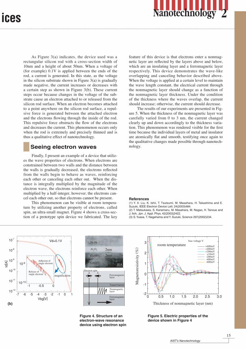
As Figure 3(a) indicates, the device used was a rectangular silicon rod with a cross-section width of 10nm and a height of about 50nm. When a voltage of (for example) 0.1V is applied between the ends of the rod, a current is generated. In this state, as the voltage in the silicon substrate shown in Figure 3(a) is gradually made negative, the current increases or decreases with a certain step as shown in Figure 3(b). These current steps occur because changes in the voltage of the sub-strate cause an electron attached to or released from the silicon rod surface. When an electron becomes attached to a point anywhere on the silicon rod surface, a repul-sive force is generated between the attached electron and the electrons flowing through the inside of the rod. This repulsive force obstructs the flow of the electrons and decreases the current. This phenomenon occurs only when the rod is extremely and precisely thinned and is thus a qualitative effect of nanotechnology.
Seeing electron waves
������ Finally, I present an example of a device that utiliz-es the wave properties of electrons. When electrons are constrained between two walls and the distance between the walls is gradually decreased, the electrons reflected from the walls begin to behave as waves, reinforcing each other or canceling each other out. When the dis-tance is integrally multiplied by the magnitude of the electron wave, the electrons reinforce each other. When multiplied by a half-integer, however, the electrons can-cel each other out, so that electrons cannot be present. This phenomenon can be visible at room tempera-ture by utilizing another property of electrons, called spin, an ultra-small magnet. Figure 4 shows a cross-sec-tion of a prototype spin device we fabricated. The key
feature of this device is that electrons enter a nonmag-netic layer are reflected by the layers above and below, which are an insulating layer and a ferromagnetic layer respectively. This device demonstrates the wave-like overlapping and canceling behavior described above. When the voltage is applied at a certain level to maintain the wave length constant, the electrical current through the nonmagnetic layer should change as a function of the nonmagnetic layer thickness. Under the condition of the thickness where the waves overlap, the current should increase; otherwise, the current should decrease. The results of our experiments are presented in Fig-ure 5. When the thickness of the nonmagnetic layer was carefully varied from 0 to 3 nm, the current changed clearly up and down accordingly to the thickness varia-tion. This phenomenon was rendered visible for the first time because the individual layers of metal and insulator are atomically flat and smooth, testifying once again to the qualitative changes made possible through nanotech-nology.
References(1) Y. X. Liu, K. Ishii, T. Tsutsumi, M. Masahara, H. Takashima and E. Suzuki, IEEE Electron Device Lett. 24(2003)484.(2) T. Matsukawa, S. Kanemaru, M. Masahara, M. Nagao, H. Tanoue and J. Itoh, Jpn. J. Appl. Phys. 42(2003)2422.(3) S. Yuasa, T. Nagahama and Y. Suzuki, Science 297(2002)234.

2,3,7,8-TCDD-binding protein
2,3,7,8-TCDD
anti-dioxin antibody
nanostructure
QCMImmobilized
Quartz crystal oscillator(QCM) electrode
Figure 1. Development of a highly sensitive environmental measurement sensor.Nanoscale structures are formed on the electrodes of quartz crystal microbalance. These surfaces are densely embedded with biofunctional substances such as receptors and artificial antibodies.
Dioxin measurement chip(QCM、0.8cm)
1cm
Battery drive type(6×4.5×3 cm)130 g (Total weight)
DXN SensorReaction space (mesoporous)
Titania (nano-sized particle)
Selectivity inducing molecule
Photo catalyst
Detoxificationexcited bysunlight
300 400 500 6000
0.2
0.4
wavelength(nm)
TiO2
present
previous
nanostructured photocatalyst
Development of visible-light reactive photocatalyst
NO
rem
oval
toluenexylene
formaldehyde
Figure 2. Detoxification of harmful chemicals using advanced functional photocatalysts
Photo 2. Photocatalytic materials spread out on a street
Photo 1. Simple quartz crystal oscillator–type dioxin measuring instrument
16AIST’s Nanotechnology
he nanotech revolution, which has made as-tounding progress in recent years, is spreading to the field of environmental technology. Hap-
hazard approaches to environmental measures are a significant factor behind rising costs in manufacturing. To prevent these costs from diminishing Japan’s indus-trial competitiveness, new ideas in nanotechnology need to be matched with the enterprises that require them, generating effective and radical technology change in the environmental field and developing the field of en-vironmental services—a business with a huge potential market. The essential point in general chemical risk man-agement is to minimize the costs of management. These costs include the cost of equipment and facilities used in monitoring, measurement and processing, as well as the energy and reagents used to run and maintain systems. The following article is a review of recent developments and research trends in monitoring and measuring tech-nologies, processing technologies applied in the use of chemicals and emission of waste, and some innovative clean-manufacturing technologies.
Development of on-site, real-time environmental measurement devices
Environmental measurement is crucial in determin-ing how chemicals pollute the environment. For exam-ple, assessing where groundwater and soil are polluted and with what pollutants is extremely costly, as it is time-consuming and requires a great range of measuring instruments. Industries need measuring devices that are simple, flexible and compact. As Figure 1 illustrates, one instrument has been developed which consists of a quartz crystal microbalance modified with proteins and
lipids that detect dioxin and trichloroethylene. When the instrument captures chemicals, the resulting increase in weight generates a change in oscillating frequency by which the chemicals are detected. This simple and high-ly sensitive sensor is now finding practical applications (Photo.1). A number of approaches are being developed that aim to reproduce in microchips the molecular recogni-tion systems of living creatures. One technology freely arrays and integrates electrodes within a microchip sys-tem. Another forms nanoscale structures on the surfaces of each of the electrodes thus arrayed; these structures are fitted with high-density arrays of substances with biological functions, such as receptors, enzymes and ar-tificial antibodies, or are covered in inorganic catalysts. In another technology, functions such as reaction, sepa-ration and detection on the surfaces of each individual electrode are controlled electrically.
Development of environmental cleanup technologies for processes in which harmful chemicals are used and emitted
In addition to well-known pollutants such as ni-trogen oxides (NOx), sulphur oxides (SOx) and carbon monooxide (CO), which are generated and released in the burning of fossil fuels, many SMEs’ plants use chemicals such as toluene, xylene and dichloromethane as solvents and cleaning agents. Households use agents such as formaldehyde (adhesive solvents and resins) and p-dichlorobenzene (pesticides). Because most of these pollutants are discarded into the environment at room temperatures, the chemical industry is looking for ways of processing them as close to room temperatures
Takashi IBUSUKI, Institute for Environmental Management Technology
Managing Chemical Risks Using Environment al Nanotechnology
Top
ics
T
Fabrication of multifunctional integrated nanocatalyst
Preparation of multi-functional integrated catalyst
Highly dispersedkeeping the composition
Adsorption/decomposition system at low temperature
Support
O2
H* O*
Direct HydroxylationAromatic compound
(Benzene)Aromatic Alcohol
(Phenol)
OH
Single-step synthesis
One-Pass Yield10%
Special Reaction Sitefor Oxygen Activation
(Low temperature reaction Safety)
Membrane for Hydrogen Permeation Hydrogen separation Permeation and Activation Catalytic Function
Figure 4. Development of a one-step process for synthesis of propylene oxide (PO) (Research Institute for Green Technology)
Figure 3. Processing of harmful chemicals using catalysts with controlled nanopores and nanostructures (Research Institute for Green Technology)
Figure 5. Development of a one-step process for synthesis of phenol using nanomembranes (Laboratory for Membrane Chemistry)
O
O O
PO:4 million ton/yearraw materials for raw materials for urethane etc.
2.2 t /1t (PO)E factor=2.2
O
O
E factor = 0.3 or 0 (calculated)
O
17AIST’s Nanotechnology
Managing Chemical Risks Using Environment al Nanotechnology
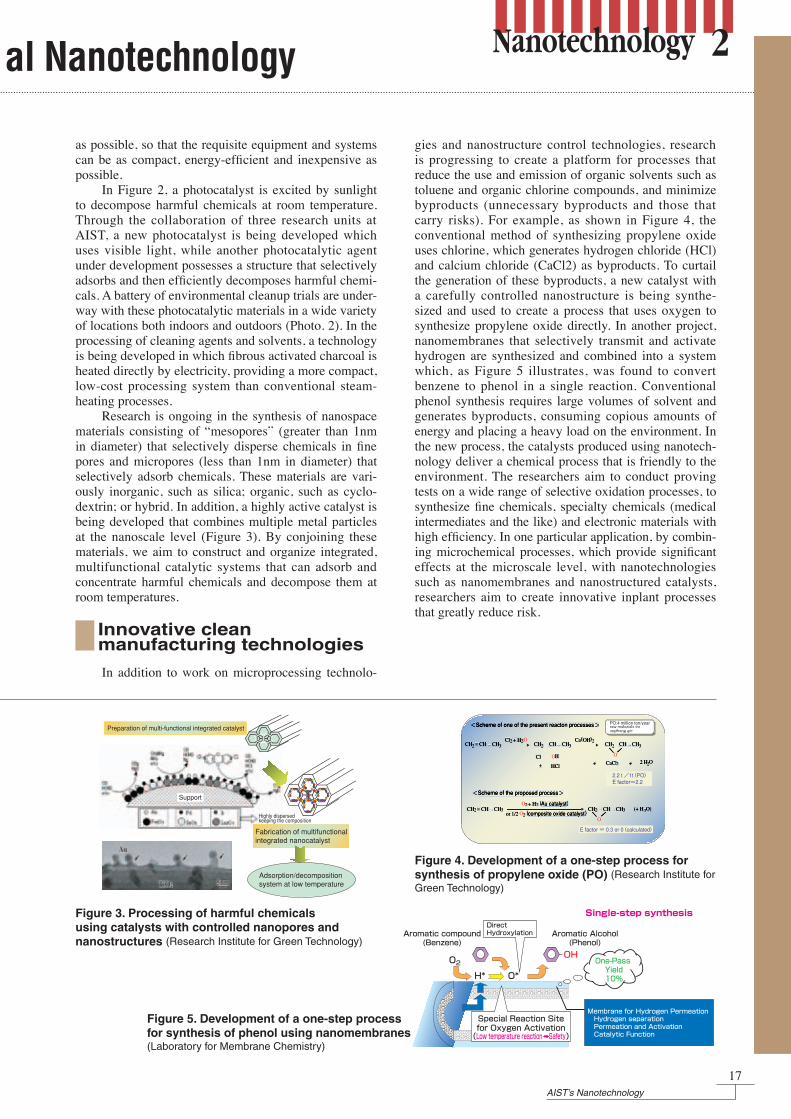
as possible, so that the requisite equipment and systems can be as compact, energy-efficient and inexpensive as possible. In Figure 2, a photocatalyst is excited by sunlight to decompose harmful chemicals at room temperature. Through the collaboration of three research units at AIST, a new photocatalyst is being developed which uses visible light, while another photocatalytic agent under development possesses a structure that selectively adsorbs and then efficiently decomposes harmful chemi-cals. A battery of environmental cleanup trials are under-way with these photocatalytic materials in a wide variety of locations both indoors and outdoors (Photo. 2). In the processing of cleaning agents and solvents, a technology is being developed in which fibrous activated charcoal is heated directly by electricity, providing a more compact, low-cost processing system than conventional steam-heating processes. Research is ongoing in the synthesis of nanospace materials consisting of “mesopores” (greater than 1nm in diameter) that selectively disperse chemicals in fine pores and micropores (less than 1nm in diameter) that selectively adsorb chemicals. These materials are vari-ously inorganic, such as silica; organic, such as cyclo-dextrin; or hybrid. In addition, a highly active catalyst is being developed that combines multiple metal particles at the nanoscale level (Figure 3). By conjoining these materials, we aim to construct and organize integrated, multifunctional catalytic systems that can adsorb and concentrate harmful chemicals and decompose them at room temperatures.
Innovative clean manufacturing technologies
In addition to work on microprocessing technolo-
gies and nanostructure control technologies, research is progressing to create a platform for processes that reduce the use and emission of organic solvents such as toluene and organic chlorine compounds, and minimize byproducts (unnecessary byproducts and those that carry risks). For example, as shown in Figure 4, the conventional method of synthesizing propylene oxide uses chlorine, which generates hydrogen chloride (HCl) and calcium chloride (CaCl2) as byproducts. To curtail the generation of these byproducts, a new catalyst with a carefully controlled nanostructure is being synthe-sized and used to create a process that uses oxygen to synthesize propylene oxide directly. In another project, nanomembranes that selectively transmit and activate hydrogen are synthesized and combined into a system which, as Figure 5 illustrates, was found to convert benzene to phenol in a single reaction. Conventional phenol synthesis requires large volumes of solvent and generates byproducts, consuming copious amounts of energy and placing a heavy load on the environment. In the new process, the catalysts produced using nanotech-nology deliver a chemical process that is friendly to the environment. The researchers aim to conduct proving tests on a wide range of selective oxidation processes, to synthesize fine chemicals, specialty chemicals (medical intermediates and the like) and electronic materials with high efficiency. In one particular application, by combin-ing microchemical processes, which provide significant effects at the microscale level, with nanotechnologies such as nanomembranes and nanostructured catalysts, researchers aim to create innovative inplant processes that greatly reduce risk.
Reaction Path
2HCOOH(g)
2HCOOH(ad)
H2O desorb
Energy ( eV)
-3
-2
-1
0
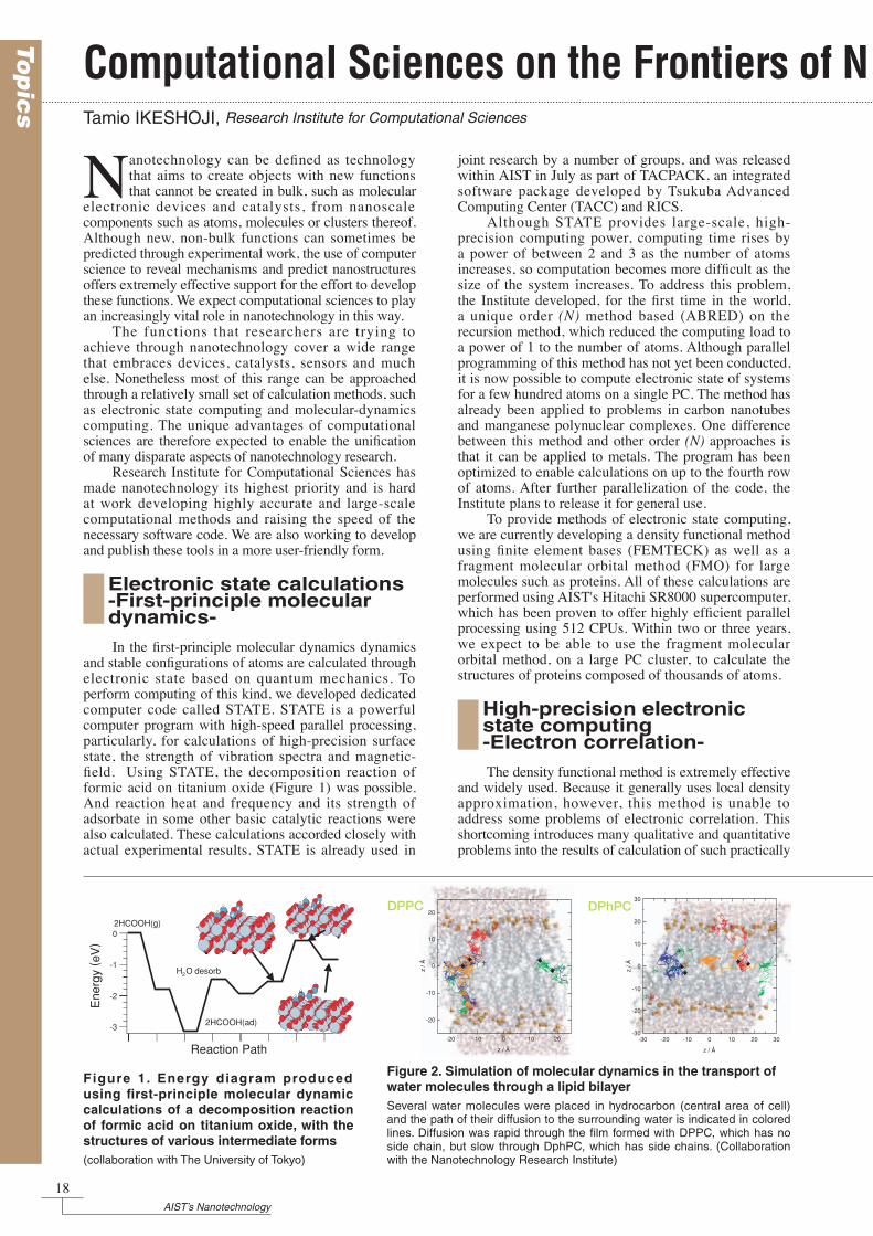
Figure 1. Energy diagram produced using first-principle molecular dynamic calculations of a decomposition reaction of formic acid on titanium oxide, with the structures of various intermediate forms (collaboration with The University of Tokyo)
Figure 2. Simulation of molecular dynamics in the transport of water molecules through a lipid bilayerSeveral water molecules were placed in hydrocarbon (central area of cell) and the path of their diffusion to the surrounding water is indicated in colored lines. Diffusion was rapid through the film formed with DPPC, which has no side chain, but slow through DphPC, which has side chains. (Collaboration with the Nanotechnology Research Institute)
x / ナ
-30 -20 -10 0 10 20 30-30
-20
-10
0
10
20
30
z / Å
z / Å
-20 -10 0 10 20
-20
-10
0
10
20
z / Å
z / Å
DPPC DPhPC
18AIST’s Nanotechnology
anotechnology can be defined as technology that aims to create objects with new functions that cannot be created in bulk, such as molecular
electronic devices and catalysts, from nanoscale components such as atoms, molecules or clusters thereof. Although new, non-bulk functions can sometimes be predicted through experimental work, the use of computer science to reveal mechanisms and predict nanostructures offers extremely effective support for the effort to develop these functions. We expect computational sciences to play an increasingly vital role in nanotechnology in this way. The functions that researchers are trying to achieve through nanotechnology cover a wide range that embraces devices, catalysts, sensors and much else. Nonetheless most of this range can be approached through a relatively small set of calculation methods, such as electronic state computing and molecular-dynamics computing. The unique advantages of computational sciences are therefore expected to enable the unification of many disparate aspects of nanotechnology research. Research Institute for Computational Sciences has made nanotechnology its highest priority and is hard at work developing highly accurate and large-scale computational methods and raising the speed of the necessary software code. We are also working to develop and publish these tools in a more user-friendly form.
Electronic state calculations -First-principle molecular dynamics- In the first-principle molecular dynamics dynamics and stable configurations of atoms are calculated through electronic state based on quantum mechanics. To perform computing of this kind, we developed dedicated computer code called STATE. STATE is a powerful computer program with high-speed parallel processing, particularly, for calculations of high-precision surface state, the strength of vibration spectra and magnetic-field. Using STATE, the decomposition reaction of formic acid on titanium oxide (Figure 1) was possible. And reaction heat and frequency and its strength of adsorbate in some other basic catalytic reactions were also calculated. These calculations accorded closely with actual experimental results. STATE is already used in
joint research by a number of groups, and was released within AIST in July as part of TACPACK, an integrated software package developed by Tsukuba Advanced Computing Center (TACC) and RICS. Although STATE provides large-scale, high-precision computing power, computing time rises by a power of between 2 and 3 as the number of atoms increases, so computation becomes more difficult as the size of the system increases. To address this problem, the Institute developed, for the first time in the world, a unique order (N) method based (ABRED) on the recursion method, which reduced the computing load to a power of 1 to the number of atoms. Although parallel programming of this method has not yet been conducted, it is now possible to compute electronic state of systems for a few hundred atoms on a single PC. The method has already been applied to problems in carbon nanotubes and manganese polynuclear complexes. One difference between this method and other order (N) approaches is that it can be applied to metals. The program has been optimized to enable calculations on up to the fourth row of atoms. After further parallelization of the code, the Institute plans to release it for general use. To provide methods of electronic state computing, we are currently developing a density functional method using finite element bases (FEMTECK) as well as a fragment molecular orbital method (FMO) for large molecules such as proteins. All of these calculations are performed using AIST's Hitachi SR8000 supercomputer, which has been proven to offer highly efficient parallel processing using 512 CPUs. Within two or three years, we expect to be able to use the fragment molecular orbital method, on a large PC cluster, to calculate the structures of proteins composed of thousands of atoms.
High-precision electronic state computing -Electron correlation- The density functional method is extremely effective and widely used. Because it generally uses local density approximation, however, this method is unable to address some problems of electronic correlation. This shortcoming introduces many qualitative and quantitative problems into the results of calculation of such practically
Tamio IKESHOJI, Research Institute for Computational Sciences
Computational Sciences on the Frontiers of N anotechnology
Top
ics
N
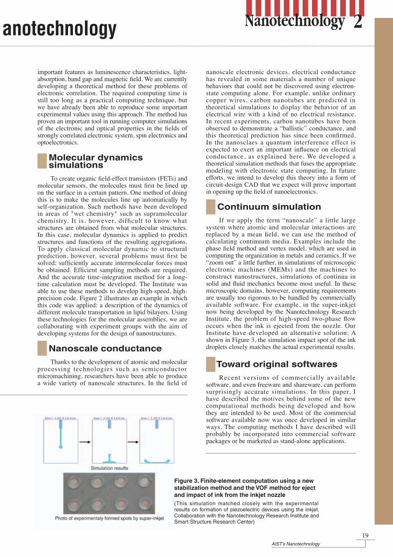
Figure 3. Finite-element computation using a new stabilization method and the VOF method for eject and impact of ink from the inkjet nozzle(This simulation matched closely with the experimental results on formation of piezoelectric devices using the inkjet. Collaboration with the Nanotechnology Research Institute and Smart Structure Research Center)
19AIST’s Nanotechnology
Computational Sciences on the Frontiers of N anotechnology
important features as luminescence characteristics, light-absorption, band gap and magnetic field. We are currently developing a theoretical method for these problems of electronic correlation. The required computing time is still too long as a practical computing technique, but we have already been able to reproduce some important experimental values using this approach. The method has proven an important tool in running computer simulations of the electronic and optical properties in the fields of strongly correlated electronic system, spin electronics and optoelectronics.
Molecular dynamics simulations To create organic field-effect transistors (FETs) and molecular sensors, the molecules must first be lined up on the surface in a certain pattern. One method of doing this is to make the molecules line up automatically by self-organization. Such methods have been developed in areas of "wet chemistry" such as supramolecular chemistry. It is, however, difficult to know what structures are obtained from what molecular structures. In this case, molecular dynamics is applied to predict structures and functions of the resulting aggregations. To apply classical molecular dynamic to structural prediction, however, several problems must first be solved; sufficiently accurate intermolecular forces must be obtained. Efficient sampling methods are required. And the accurate time-integration method for a long-time calculation must be developed. The Institute was able to use these methods to develop high-speed, high-precision code. Figure 2 illustrates an example in which this code was applied: a description of the dynamics of different molecule transportation in lipid bilayers. Using these technologies for the molecular assemblies, we are collaborating with experiment groups with the aim of developing systems for the design of nanostructures.
Nanoscale conductance Thanks to the development of atomic and molecular processing technologies such as semiconductor micromachining, researchers have been able to produce a wide variety of nanoscale structures. In the field of
nanoscale electronic devices, electrical conductance has revealed in some materials a number of unique behaviors that could not be discovered using electron-state computing alone. For example, unlike ordinary copper wires, carbon nanotubes are predicted in theoretical simulations to display the behavior of an electrical wire with a kind of no electrical resistance. In recent experiments, carbon nanotubes have been observed to demonstrate a “ballistic” conductance, and this theoretical prediction has since been confirmed. In the nanosclaes a quantum interference effect is expected to exert an important influence on electrical conductance, as explained here. We developed a theoretical simulation methods that fuses the appropriate modeling with electronic state computing. In future efforts, we intend to develop this theory into a form of circuit-design CAD that we expect will prove important in opening up the field of nanoelectronics.
Continuum simulation If we apply the term “nanoscale” a little large system where atomic and molecular interactions are replaced by a mean field, we can use the method of calculating continuum media. Examples include the phase field method and vertex model, which are used in computing the organization in metals and ceramics. If we “zoom out” a little further, in simulations of microscopic electronic machines (MEMs) and the machines to construct nanostructures, simulations of continua in solid and fluid mechanics become most useful. In these microscopic domains, however, computing requirements are usually too rigorous to be handled by commercially available software. For example, in the super-inkjet now being developed by the Nanotechnology Research Institute, the problem of high-speed two-phase flow occurs when the ink is ejected from the nozzle. Our Institute have developed an alternative solution; A shown in Figure 3, the simulation impact spot of the ink droplets closely matches the actual experimental results.
Toward original softwares Recent versions of commercially available software, and even freeware and shareware, can perform surprisingly accurate simulations. In this paper, I have described the motives behind some of the new computational methods being developed and how they are intended to be used. Most of the commercial software available now was once developed in similar ways. The computing methods I have described will probably be incorporated into commercial software packages or be marketed as stand-alone applications.

he Nanotechnology Program was launched in 2001 to create a platform technology that will contribute to the sustainable development of Ja-
pan’s economy and to incubate new businesses that will lead the world market in nanotechnology and nanoma-terials in 10 years’ time. The Nanotechnology Program consists of a number of projects, including nine projects involved in the Nanomaterials and Processing Sub-Program Projects and four projects involved in the Nano Manufacturing and Metrology Sub-Program Projects. NEDO manages these projects as the entrusted mis-sion from the Ministry of Economy, Trade and Industry (METI). The Nanotechnology and Materials Technol-ogy Development Department (NMTDD) is in charge of all the Nanomaterials and Processing Sub-Program Projects; two of the Nano Manufacturing and Metrology Sub-Program Projects; and four of “Focus 21” projects started this fiscal year of 2003 (for details, please see the illustrations below). The NMTDD is tasked with management of the project in accordance with the following management policies, as is reflected in the agreements signed with each of the project contractors.
Promoting the commercialization
(1) By the end of the third fiscal year of the project, at
least one prototype (sample material, database, or simu-lation software, etc) that can be used for trial purposes must be produced and it will be furnished to outside ob-servers after closing a contract.(2) Each participant of the project may request the con-sent of other participants for the use of said participants’ patents or expertise if it is required for carrying out the project.
Promoting the dissemination of information
(1) The NMTDD operates a domestic mailing list called the Nano-Tech Mailing List, to provide information exchange on nanotechnology to persons interested in nanotechnology, both within and outside the Nanotech-nology Program. As of June 2003, this mailing list has approximately 760 members. Every effort will be made to provide comprehensive disclosure on the NEDO web-site.(2) Forums, workshops, exhibitions and similar kinds of events will be held every year. Research activities are also conducted for aiming at developing practical appli-cations and commercialization of nanotechnology.(3) An international network of professionals will be formed to promote R&D and commercialization of nanotechnology through the free and open exchange of views and information among people.
Kyouhei NISHIDANanotechnology and Materials Technology Development Department,New Energy and Industrial Technology Development Organization (NEDO)
The Nanotechnology Program Projects and NEDO's Project Management
Project FY2000 FY2001 FY2002 FY2003 FY2004 FY2005 FY2006 FY2007
Nanostructure Polymer Project
Nanotechnology Glass Project
Nanotechnology Glass Project for Display
Nanotechnology Glass Project for Electron Device
Nanotechnology Metal Project
Nanocarbon Technology Project/Advanced Nanocarbon Application Project
Carbon Nanotube FED Project
Advanced Diamond Technology Project
Nanotechnology Particle Project
Nanostructure Coating Project
Synthetic Nano-Function Materials Project
Nanotechnology Material Metrology Project
Systematization of Nanotechnology Materials Program Results Project
Sum of the budgets (million yen, 100yen=8.4USD 300
300
1300
600
300
900
500
250
230
220
4300 5480
1150
620
670
750
910
520
360
230
270
950
430
490
640
360
250
160
190
6870
250
260
1270
810
810
Table. Nanotechnology Program (Nanomaterials and Processing Sub-Program and Nanodevice and Materials Sub-Program)
20AIST’s Nanotechnology
1
2
Na
tion
al P
roje
ct
T
Mean diameter:3nmMean diameter:3nm長さLength
Macroscopically similar, while “nanoscopically” different-Key: molecular weight,regularity, localization,distribution-
Nanomaterials and Processing-from average to zero deviation (from disorder to order)
Feature: Homogeneous length, tacticity, and molecular weight at the nano-scaleEffect: Improvement of toughness, viscoelasticity and heat-resistance
Size
Feature: Homogeneous particle size at the nano-scaleEffect: Low friction spacer, variable color emitter
Distribution
Feature: Homogeneous composition and atomic/molecular distribution at the nano-scaleEffect: Crack-free glass
Mean length:10nm Mean length:10nm Mean concentration:11% Mean concentration:11%
Systematization of Nanotechnology Materials Program Results Project
Nanotechnology Material Metrology PJ
Nanotechnology Particle PJ
Nanostructure Coating PJ
Synthetic Nano-Function Materials PJ
Nanotechnology Glass PJ
Nanotechnology Metal PJ
Nanocarbon Technology PJ
(Focus21 Projects)
Nanodevice and nanomaterials for next-generation information
technology
Nanostructure Polymer PJ
Nanotechnology Glass PJ for Electron Device
Nanotechnology Glass PJ for Display
Carbon Nanotube FED PJ
Advanced Diamond Technology PJ
Nanotechnology Program - Nanomaterials and Processing Sub-Program -
Mission of Nano Manufacturing and Metrology Sub-ProgramTechnology for upgrading of manufacturing technology and multifunctionalization of nanomaterials
Technology keeping / enhancing the order of nanostructure
Miniaturization, integration and encupsulationby nanotechnology
Measurement techniques for the evaluation of processing accuracy
Clusters Nanoparticle
Upgrading for manufacturing technology
Ultrathin film
Encapsulation
Coating
Manipulation of nanomaterialswithout losing their functions
Functional ultrathin film
Strong adhesion of the coating films without losing their functions
Fine control of heterojunction interfacesat the nano-scale
Quantum beamMeasurement at the nano-scale
Nanoprocessed goodsSteps by 1 nm
Ceramics thin film at the nanometer levelSubstrate
Fast collision
Function control by ultrafine processing
Multipulication of functionsby complexation
magnification
NanomaterialsClusters Nanoparticle
Multifunctionalization of nanomaterials
Nanometal
Full Color Rewritable Paper Using Functional Capsule PJ
R & D of 3D NanoScale Certified Reference Materials PJ
Nano-Fabrication Process Technology Using Advanced Quantum Beams
R & D of 3D NanoScale Certified Reference Materials PJ
Thorough research management and promotion of liaison among projects
(1) Considerable authority will be conferred on project leaders and clear numerical targets will be set, to ensure responsible and effective research management.(2) Effective liaison among projects will be maintained through “Systematization of Nanotechnology Materials
21AIST’s Nanotechnology
Program Results Project”. During the current fiscal year, five projects will be subject to an interim evaluation: Nanotechnol-ogy Metal Project; Nanotechnology Glass Project; Nanotechnology Par-ticle Project; Nanostructure Coating Project; and Synthetic Nano-Func-tion Materials Project. Moreover, most of the projects under Nanoma-terials and Processing Sub-Program are subject to the third fiscal year, when the submission of prototypes will be required. This year is thus designated as an evaluation year, when progress in each project is verified and reviewed and future management policies and directions are determined. Full and comprehensive shar-ing and publication of information is of crucial importance, as the com-mercialization of nanotechnology research results requires timely and rapid response. Currently moves are afoot in industry in Japan to es-tablish a nanotechnology business promotion council, which NEDO believes will provide much-needed support. This fiscal year, the evalu-ation year, NEDO will be involved in “nano tech 2004”, as “nano tech 2003 + Future”. “nano tech 2004”, scheduled for March 2004 at Tokyo Big Site, is the world biggest inter-national exhibition and conference on nanotechnology providing the resources necessary to launch new and exciting nanotechnology indus-tries. NEDO is also keenly active in promoting exchanges of views through overseas expositions, in-cluding Nanofair 2003 in St. Gallen (Switzerland) slated for September 2003. Four projects under Nanoma-
terials and Processing Sub-Program and two under Nano Manufacturing and Metrology Sub-Program are led by researchers from National Institute of Advanced Indus-trial Science and Technology (AIST). In many other projects, AIST is a key participant, playing important roles in each of these efforts. I would like to close by thanking all of the researchers in advance for their valu-able work in furthering each of the projects that make up the Nanotechnology Program.
3
The materials and devices that nanotechnology has given the world are used in a wide range of systems and machines today. One of the most exciting features of nanotechnology is its astounding breadth of real and po-tential applications. Thus the propagation effect of nano-technology is immense, and the business opportunities it creates are both numerous and diverse. If the size of the nanotechnology market were calculated based on the breadth of its influence and the extent of the commercial opportunities, it renders feasible. Depending on the as-sumptions used, the market could be worth between ¥20 trillion and ¥30 trillion by 2010. A number of possible trial calculation results are presented below. In the electronics field, a vast potential market can be tentatively calculated for such products as new types of displays, secondary batteries and fuel cells, replace-ments for today’s general-purpose semiconductor mem-ory (for example, magnetoresistive random access mem-ory, or MRAM), magnetic recording devices and wiring materials. New displays are being aggressively pursued through the development of carbon nanotube applica-tions. By 2010, the market for such displays may be on the order of ¥180 billion. Carbon nanotubes and nano-horns are expected to be applied in the development of secondary batteries, used in mobile telephones, and fuel cells, which should be used in power vehicles and even at homes in the future. The market for such secondary batteries is forecast to reach ¥150 billion, while a fig-ure of ¥120 billion is anticipated for fuel cells. Another prominent example of a nanotechnology application is MRAM, which may replace existing DRAMs to create a market on the scale of ¥120 billion. This forecast covers only replacement of the latest generation of DRAMs; the figure may well grow larger if MRAMs cast into the�market and enter a true growth phase. In biotechnology area, nanotechnology will open vast opportunities for such applications as drug delivery systems. For example, microcapsules developed using
nanotechnological techniques could deliver medicines to affected areas within a patient’s body. This is an es-pecially exciting field for Japan, with its eminence in polymer chemistry. Even in fields of existing materials�such as iron and glass, nanotechnology is expected to be applied to effect quantum improvements in function and performance, blazing the trail to a multitude of fresh opportunities and sizeable new markets. For example, fine ceramics to which nanotechnology is applied is forecasted to reach production of ¥100 billion by 2010. Many nanotechnology products will be goods used in the everyday lives of consumers, such as photocatalysts and cosmetics. A trial calculation of the market for pho-tocatalysts and other environmentally friendly catalysts suggests a figure of ¥70 billion. Nanoscale particles can be used in transparent sunscreen and foundation pow-ders, generating a market of some ¥45 billion. The products to which the above trial calculations apply incorporate a great deal of processing, which im-plies a high price in many cases. The above-mentioned market size of nanotechnology reflect this value-added as well as the large size of the markets for the products in question. The trial calculation reflects the direct eco-nomic effects of nanotechnology; the actual range of the propagation effect of this technology is much broader. For example, as the markets described above are real-ized, a wide range of business opportunities are sure to emerge in the fields of related processing and mea-surement equipment. Moreover, many themes exist in which research institutions among industry, government bodies, and universities can give free rein to their own unique talents and capabilities. As they develop those abilities, new synergies should arise among the industry, government bodies, and universities, leading to a many exciting new high-tech joint ventures. This, too, is an important economic propagation effect of nanotechnol-ogy.
Naoki IKEZAWA Nomura Research Institute, Ltd.
The Propagation Effect of Nanotechnology on the Economy
22AIST’s Nanotechnology
Na
no
tec
hn
olo
gy in
Bu
sine
ss
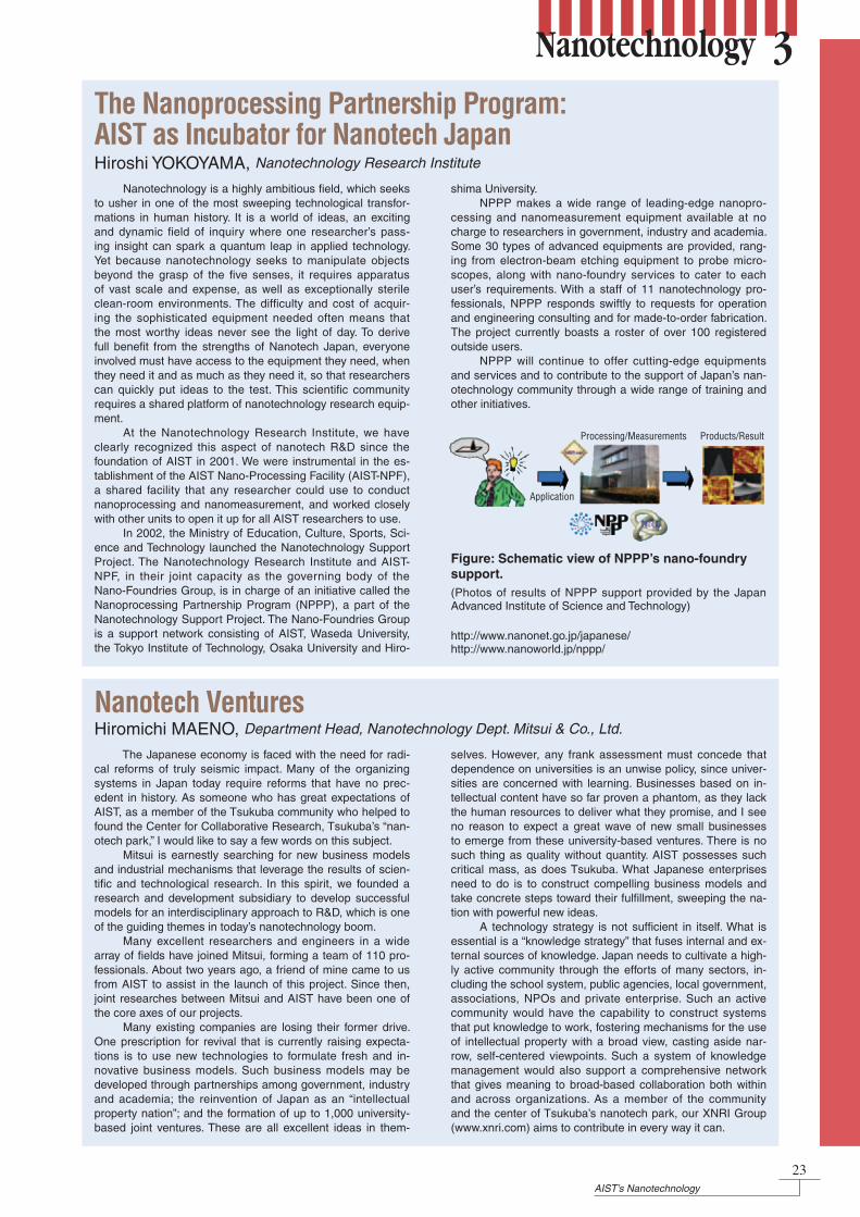
The Nanoprocessing Partnership Program: AIST as Incubator for Nanotech Japan
shima University. NPPP makes a wide range of leading-edge nanopro-cessing and nanomeasurement equipment available at no charge to researchers in government, industry and academia. Some 30 types of advanced equipments are provided, rang-ing from electron-beam etching equipment to probe micro-scopes, along with nano-foundry services to cater to each user’s requirements. With a staff of 11 nanotechnology pro-fessionals, NPPP responds swiftly to requests for operation and engineering consulting and for made-to-order fabrication. The project currently boasts a roster of over 100 registered outside users. NPPP will continue to offer cutting-edge equipments and services and to contribute to the support of Japan’s nan-otechnology community through a wide range of training and other initiatives.
Nanotechnology is a highly ambitious field, which seeks to usher in one of the most sweeping technological transfor-mations in human history. It is a world of ideas, an exciting and dynamic field of inquiry where one researcher’s pass-ing insight can spark a quantum leap in applied technology. Yet because nanotechnology seeks to manipulate objects beyond the grasp of the five senses, it requires apparatus of vast scale and expense, as well as exceptionally sterile clean-room environments. The difficulty and cost of acquir-ing the sophisticated equipment needed often means that the most worthy ideas never see the light of day. To derive full benefit from the strengths of Nanotech Japan, everyone involved must have access to the equipment they need, when they need it and as much as they need it, so that researchers can quickly put ideas to the test. This scientific community requires a shared platform of nanotechnology research equip-ment. At the Nanotechnology Research Institute, we have clearly recognized this aspect of nanotech R&D since the foundation of AIST in 2001. We were instrumental in the es-tablishment of the AIST Nano-Processing Facility (AIST-NPF), a shared facility that any researcher could use to conduct nanoprocessing and nanomeasurement, and worked closely with other units to open it up for all AIST researchers to use. In 2002, the Ministry of Education, Culture, Sports, Sci-ence and Technology launched the Nanotechnology Support Project. The Nanotechnology Research Institute and AIST-NPF, in their joint capacity as the governing body of the Nano-Foundries Group, is in charge of an initiative called the Nanoprocessing Partnership Program (NPPP), a part of the Nanotechnology Support Project. The Nano-Foundries Group is a support network consisting of AIST, Waseda University, the Tokyo Institute of Technology, Osaka University and Hiro-
Hiroshi YOKOYAMA, Nanotechnology Research Institute
Nanotech Ventures
selves. However, any frank assessment must concede that dependence on universities is an unwise policy, since univer-sities are concerned with learning. Businesses based on in-tellectual content have so far proven a phantom, as they lack the human resources to deliver what they promise, and I see no reason to expect a great wave of new small businesses to emerge from these university-based ventures. There is no such thing as quality without quantity. AIST possesses such critical mass, as does Tsukuba. What Japanese enterprises need to do is to construct compelling business models and take concrete steps toward their fulfillment, sweeping the na-tion with powerful new ideas. A technology strategy is not sufficient in itself. What is essential is a “knowledge strategy” that fuses internal and ex-ternal sources of knowledge. Japan needs to cultivate a high-ly active community through the efforts of many sectors, in-cluding the school system, public agencies, local government, associations, NPOs and private enterprise. Such an active community would have the capability to construct systems that put knowledge to work, fostering mechanisms for the use of intellectual property with a broad view, casting aside nar-row, self-centered viewpoints. Such a system of knowledge management would also support a comprehensive network that gives meaning to broad-based collaboration both within and across organizations. As a member of the community and the center of Tsukuba’s nanotech park, our XNRI Group (www.xnri.com) aims to contribute in every way it can.
The Japanese economy is faced with the need for radi-cal reforms of truly seismic impact. Many of the organizing systems in Japan today require reforms that have no prec-edent in history. As someone who has great expectations of AIST, as a member of the Tsukuba community who helped to found the Center for Collaborative Research, Tsukuba’s “nan-otech park,” I would like to say a few words on this subject. Mitsui is earnestly searching for new business models and industrial mechanisms that leverage the results of scien-tific and technological research. In this spirit, we founded a research and development subsidiary to develop successful models for an interdisciplinary approach to R&D, which is one of the guiding themes in today’s nanotechnology boom. Many excellent researchers and engineers in a wide array of fields have joined Mitsui, forming a team of 110 pro-fessionals. About two years ago, a friend of mine came to us from AIST to assist in the launch of this project. Since then, joint researches between Mitsui and AIST have been one of the core axes of our projects. Many existing companies are losing their former drive. One prescription for revival that is currently raising expecta-tions is to use new technologies to formulate fresh and in-novative business models. Such business models may be developed through partnerships among government, industry and academia; the reinvention of Japan as an “intellectual property nation”; and the formation of up to 1,000 university-based joint ventures. These are all excellent ideas in them-
Hiromichi MAENO, Department Head, Nanotechnology Dept. Mitsui & Co., Ltd.
http://www.nanonet.go.jp/japanese/http://www.nanoworld.jp/nppp/
23AIST’s Nanotechnology
Figure: Schematic view of NPPP’s nano-foundry support.(Photos of results of NPPP support provided by the Japan Advanced Institute of Science and Technology)
Processing/Measurements Products/Result
Application
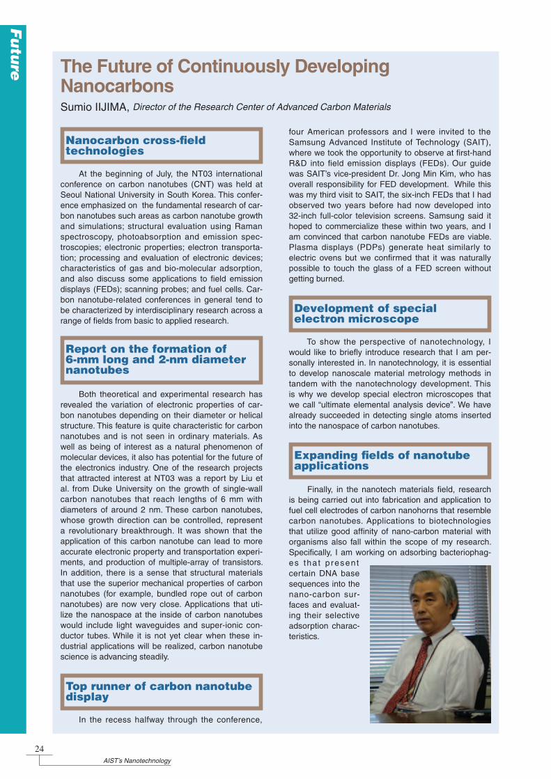
24AIST’s Nanotechnology
The Future of Continuously Developing Nanocarbons
four American professors and I were invited to the Samsung Advanced Institute of Technology (SAIT), where we took the opportunity to observe at first-hand R&D into field emission displays (FEDs). Our guide was SAIT’s vice-president Dr. Jong Min Kim, who has overall responsibility for FED development. While this was my third visit to SAIT, the six-inch FEDs that I had observed two years before had now developed into 32-inch full-color television screens. Samsung said it hoped to commercialize these within two years, and I am convinced that carbon nanotube FEDs are viable. Plasma displays (PDPs) generate heat similarly to electric ovens but we confirmed that it was naturally possible to touch the glass of a FED screen without getting burned.
To show the perspective of nanotechnology, I would like to briefly introduce research that I am per-sonally interested in. In nanotechnology, it is essential to develop nanoscale material metrology methods in tandem with the nanotechnology development. This is why we develop special electron microscopes that we call “ultimate elemental analysis device”. We have already succeeded in detecting single atoms inserted into the nanospace of carbon nanotubes.
Finally, in the nanotech materials field, research is being carried out into fabrication and application to fuel cell electrodes of carbon nanohorns that resemble carbon nanotubes. Applications to biotechnologies that utilize good affinity of nano-carbon material with organisms also fall within the scope of my research. Specifically, I am working on adsorbing bacteriophag-es tha t p resent certain DNA base sequences into the nano-carbon sur-faces and evaluat-ing their selective adsorption charac-teristics.
At the beginning of July, the NT03 international conference on carbon nanotubes (CNT) was held at Seoul National University in South Korea. This confer-ence emphasized on the fundamental research of car-bon nanotubes such areas as carbon nanotube growth and simulations; structural evaluation using Raman spectroscopy, photoabsorption and emission spec-troscopies; electronic properties; electron transporta-tion; processing and evaluation of electronic devices; characteristics of gas and bio-molecular adsorption, and also discuss some applications to field emission displays (FEDs); scanning probes; and fuel cells. Car-bon nanotube-related conferences in general tend to be characterized by interdisciplinary research across a range of fields from basic to applied research.
Both theoretical and experimental research has revealed the variation of electronic properties of car-bon nanotubes depending on their diameter or helical structure. This feature is quite characteristic for carbon nanotubes and is not seen in ordinary materials. As well as being of interest as a natural phenomenon of molecular devices, it also has potential for the future of the electronics industry. One of the research projects that attracted interest at NT03 was a report by Liu et al. from Duke University on the growth of single-wall carbon nanotubes that reach lengths of 6 mm with diameters of around 2 nm. These carbon nanotubes, whose growth direction can be controlled, represent a revolutionary breakthrough. It was shown that the application of this carbon nanotube can lead to more accurate electronic property and transportation experi-ments, and production of multiple-array of transistors. In addition, there is a sense that structural materials that use the superior mechanical properties of carbon nanotubes (for example, bundled rope out of carbon nanotubes) are now very close. Applications that uti-lize the nanospace at the inside of carbon nanotubes would include light waveguides and super-ionic con-ductor tubes. While it is not yet clear when these in-dustrial applications will be realized, carbon nanotube science is advancing steadily.
In the recess halfway through the conference,
Sumio IIJIMA, Director of the Research Center of Advanced Carbon Materials
Nanocarbon cross-field technologies
Report on the formation of 6-mm long and 2-nm diameter nanotubes
Top runner of carbon nanotube display
Development of special electron microscope
Expanding fields of nanotube applications
Fu
ture

AIST’s Nanotechnology Technical Development Outlook
to fruition, but there are also many fields where basic research can find quick practical application. By the li-aison of its research departments, Intellectual Property Division, TLOs (AIST Innovations), and the Innovation Center for Start-ups, AIST is building a system that can provide rapid support across the whole spectrum, from the search for promising research results, to their implementation.
To rapidly boost nanotechnology development, we believe it is necessary to train nanotech personnel and actively appeal to industry. Through the Nanoprocess-ing Partnership Program and the Innovative MEMS Business Support Program, we are stepping up techni-cal support of researchers in industry, providing with the latest nanoprocessing and measurement equip-ments and as well showing the operation know-hows. We also plan to exhibit in various nanotechnology-related trade fairs and actively organize nanotechnol-ogy seminars. AIST has been a world-leading pioneer in nano-technology through pursuing several nanotechnology-related projects such as the Atom Technology Project, accumulating a range of results and know-how. In its history, AIST has made it clear that nanotechnology is not only for the hi-tech world but also extends to ener-gy-saving and environment friendly technologies, new biotechnologies, and innovative production processes that result in high-quality component materials. Based on the research results achieved to date, AIST will continue to aim for further breakthroughs that contrib-ute to the development of the nanotechnology industry.
AIST is developing a policy of merging subdivided areas of knowledge and establishing an integrated system in which a wide range of researchers from dif-ferent fields can work on specific research topics. With “Type-II Basic Research”1) as the core axis, continuous research, from “Type-I Basic Research”2) up to de-velopment, will be performed as “Full-Research”. By relating this to its liaison functions with industry, gov-ernment, and universities, AIST hopes to boost the de-velopment of industrial technology. “Full-Research” is involving in the integration of a wide range of research fields, so that AIST is advantageous. Nanotechnology holds out great promise as one of the core technolo-gies of this approach.
In nanotechnology research, there are three main needs: a strong need to produce new concepts by merging different research fields together, the need for a concentrated approach focused on clear goals, and the need for close collaboration among research-ers under strong leadership. In addition to the nano-technology, materials, and manufacturing fields, AIST embraces such fields as life-science, information tech-nology, energy, environment, standards and metrol-ogy, and has developed an environment conducive to cross-field joint research with researchers from outside the nanotech field. Promoting interdisciplinary joint research with researchers in the above areas, AIST aims to establish an industrial infrastructure — nano-industry — from nanotechnology. AIST also promotes the establishment of the special research style in nan-otechnology, the computer-aided nanotechnology, by encouraging its talented human resources in computa-tional science to participate in nanotechnology-related research.
Technology licensing is an important issue for AIST. Because that nanotechnology is regarded as one of the “aces in the hole” reinforcing the com-petitiveness of Japanese industry, it is vital to promote nanotechnology research with concrete views for practical and industrial applications. Nanotechnol-ogy includes many research fields that need long-term perspective and a considerable period to come
Kazuo IGARASHI, Research Coordinator
25AIST’s Nanotechnology
1) Type-II Basic Research: Motivated by certain economic and social needs, research that combines various pieces of already established universal knowledge (including theories, natural laws, principles, and theorems), performs repeated observations, experimentation, and theoretical calculations, and by these methods and results derives regular and universal knowledge and a specific path to realize certain goals.2) Type-I Basic Research: Research to discover, interpret, and form universal theories (including natural laws, principles, and theorems) through observation, experimentation, and theoretical calculation of unknown phenomena.
“Full-Research” from nanotechnology
From nanotechnology, to nano-industry
Fierce development competition needs smooth technology transfer
Rapidly boosting nanotech development

26AIST’s Nanotechnology


Edition and Publication :Publication Office, Information & Publication Division, Public Relations DepartmentNational Institute of Advanced Industrial Science and Technology (AIST)
AIST Tsukuba Central 3, 1-1-1 Umezono, Tsukuba, Ibaraki 305-8563, JapanTEL: +81-29-861-4128 FAX: +81-29-861-4129 Email: [email protected] URL: http://www.aist.go.jp/• Reproduction in whole or in part without written permission is prohibited.• Contribution and remarks from other organizations don’t represent with AIST's views.


