Semiconductor Group 1 10.94 ● High Performance 16-bit CPU with 4-Stage Pipeline ● 100 ns Instruction Cycle Time at 20 MHz CPU Clock ● 500 ns Multiplication (16 × 16 bits), 1 μs Division (32 / 16 bit) ● Enhanced Boolean Bit Manipulation Facilities ● Register-Based Design with Multiple Variable Register Banks ● Single-Cycle Context Switching Support ● Up to 256 KBytes Linear Address Space for Code and Data ● 1 KByte On-Chip RAM ● 32 KBytes On-Chip ROM (SAB 83C166W only) ● Programmable External Bus Characteristics for Different Address Ranges ● 8-Bit or 16-Bit External Data Bus ● Multiplexed or Demultiplexed External Address/Data Buses ● Hold and Hold-Acknowledge Bus Arbitration Support ● 512 Bytes On-Chip Special Function Register Area ● Idle and Power Down Modes ● 8-Channel Interrupt-Driven Single-Cycle Data Transfer Facilities via Peripheral Event Controller (PEC) ● 16-Priority-Level Interrupt System ● 10-Channel 10-bit A/D Converter with 9.7 μs Conversion Time ● 16-Channel Capture/Compare Unit ● Two Multi-Functional General Purpose Timer Units with 5 Timers ● Two Serial Channels (USARTs) ● Programmable Watchdog Timer ● Up to 76 General Purpose I/O Lines ● Direct clock input without prescaler ● Supported by a Wealth of Development Tools like C-Compilers, Macro-Assembler Packages, Emulators, Evaluation Boards, HLL-Debuggers, Simulators, Logic Analyzer Disassemblers, Programming Boards ● On-Chip Bootstrap Loader ● 100-Pin Plastic MQFP Package (EIAJ) C16x-Family of High-Performance CMOS 16-Bit Microcontrollers Preliminary SAB 80C166W/83C166W / 83C166W 16-Bit Microcontroller SAB 80C166W/ 83C166W/ 83C166W
Transcript
Semiconductor Group 1 10.94
High Performance 16-bit CPU with 4-Stage Pipeline 100 ns Instruction Cycle Time at 20 MHz CPU Clock 500 ns Multiplication (16 × 16 bits), 1 µs Division (32 / 16 bit) Enhanced Boolean Bit Manipulation Facilities Register-Based Design with Multiple Variable Register Banks Single-Cycle Context Switching Support Up to 256 KBytes Linear Address Space for Code and Data 1 KByte On-Chip RAM 32 KBytes On-Chip ROM (SAB 83C166W only) Programmable External Bus Characteristics for Different Address Ranges 8-Bit or 16-Bit External Data Bus Multiplexed or Demultiplexed External Address/Data Buses Hold and Hold-Acknowledge Bus Arbitration Support 512 Bytes On-Chip Special Function Register Area Idle and Power Down Modes 8-Channel Interrupt-Driven Single-Cycle Data Transfer Facilities via Peripheral Event
Controller (PEC) 16-Priority-Level Interrupt System 10-Channel 10-bit A/D Converter with 9.7 µs Conversion Time 16-Channel Capture/Compare Unit Two Multi-Functional General Purpose Timer Units with 5 Timers Two Serial Channels (USARTs) Programmable Watchdog Timer Up to 76 General Purpose I/O Lines Direct clock input without prescaler Supported by a Wealth of Development Tools like C-Compilers, Macro-Assembler Packages,
The SAB 80C166W/83C166W is a representative of the Siemens SAB 80C166 family of fullfeatured single-chip CMOS microcontrollers. It combines high CPU performance (up to 10 millioninstructions per second) with high peripheral functionality and enhanced IO-capabilities. Thesedevices derive the CPU clock signal (operating clock) directly from the on-chip oscillator withoutusing a prescaler. This reduces the device’s EME.
Figure 1Logic Symbol
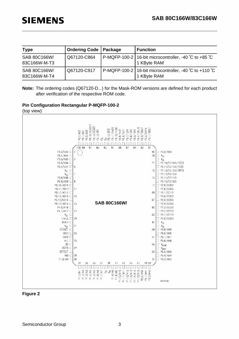
Ordering Information
Type Ordering Code Package Function
SAB 83C166W-5M On Request P-MQFP-100-2 16-bit microcontroller, 0 ˚C to +70 ˚C,1 KByte RAM and 32 KByte ROM
SAB 83C166W-5M-T3
Q67120-D... P-MQFP-100-2 16-bit microcontroller, -40 ˚C to +85 ˚C,1 KByte RAM and 32 KByte ROM
SAB 83C166W-5M-T4
Q67120-D... P-MQFP-100-2 16-bit microcontroller, -40 ˚C to +110 ˚C1 KByte RAM and 32 KByte ROM
SAB 80C166W/83C166W-M
On Request P-MQFP-100-2 16-bit microcontroller, 0 ˚C to +70 ˚C1 KByte RAM
SAB80C166W
SAB 80C166W/83C166W
Semiconductor Group 3
Note: The ordering codes (Q67120-D...) for the Mask-ROM versions are defined for each productafter verification of the respective ROM code.
Port 4 is a 2-bit bidirectional I/O port. It is bit-wiseprogrammable for input or output via direction bits. For a pinconfigured as input, the output driver is put into high-impedance state.In case of an external bus configuration, Port 4 can be used tooutput the segment address lines:P4.0 A16 Least Significant Segment Addr. LineP4.1 A17 Most Significant Segment Addr. Line
20
19
XTAL1
XTAL2
I
O
XTAL1: Input to the oscillator amplifier and input to theinternal clock generator
XTAL2: Output of the oscillator amplifier circuit.To clock the device from an external source, drive XTAL1,while leaving XTAL2 unconnected. Minimum and maximumhigh/low and rise/fall times specified in the AC Characteristicsmust be observed.
222324
BUSACT,EBC1,EBC0
III
External Bus Configuration selection inputs. These pins aresampled during reset and select either the single chip mode orone of the four external bus configurations:BUSACT EBC1 EBC0 Mode/Bus Configuration0 0 0 8-bit demultiplexed bus0 0 1 8-bit multiplexed bus0 1 0 16-bit muliplexed bus0 1 1 16-bit demultiplexed bus1 0 0 Single chip mode1 0 1 Reserved.1 1 0 Reserved.1 1 1 Reserved.ROMless versions must have pin BUSACT tied to ‘0’.
27 RSTIN I Reset Input with Schmitt-Trigger characteristics. A low levelat this pin for a specified duration while the oscillator is runningresets the SAB 80C166W/83C166W. An internal pullupresistor permits power-on reset using only a capacitorconnected to VSS.
28 RSTOUT O Internal Reset Indication Output . This pin is set to a lowlevel when the part is executing either a hardware-, asoftware- or a watchdog timer reset. RSTOUT remains lowuntil the EINIT (end of initialization) instruction is executed.
SAB 80C166W/83C166W
Semiconductor Group 5
29 NMI I Non-Maskable Interrupt Input. A high to low transition at thispin causes the CPU to vector to the NMI trap routine. Whenthe PWRDN (power down) instruction is executed, the NMI pinmust be low in order to force the SAB 80C166W/83C166W togo into power down mode. If NMI is high, when PWRDN isexecuted, the part will continue to run in normal mode.If not used, pull NMI high externally.
29 ALE O Address Latch Enable Output. Can be used for latching theaddress into external memory or an address latch in themultiplexed bus modes.
26 RD O External Memory Read Strobe. RD is activated for everyexternal instruction or data read access.
30 - 3740 - 47
P1.0 –P1.15
I/O Port 1 is a 16-bit bidirectional I/O port. It is bit-wiseprogrammable for input or output via direction bits. For a pinconfigured as input, the output driver is put into high-impedance state. Port 1 is used as the 16-bit address bus (A)in demultiplexed bus modes and also after switching from ademultiplexed bus mode to a multiplexed bus mode..
48 - 5356 - 59
P5.0 –P5.9
II
Port 5 is a 10-bit input-only port with Schmitt-Triggercharacteristics. The pins of Port 5 also serve as the (up to 10)analog input channels for the A/D converter, where P5.xequals ANx (Analog input channel x).
62 - 77
62
75
76
77
P2.0 –P2.15
I/O
I/O
I/OOI/OOI/OI
Port 2 is a 16-bit bidirectional I/O port. It is bit-wiseprogrammable for input or output via direction bits. For a pinconfigured as input, the output driver is put into high-impedance state.The following Port 2 pins also serve for alternate functions:P2.0 CC0IO CAPCOM: CC0 Cap.-In/Comp.Out... ... ...P2.13 CC13IO CAPCOM: CC13 Cap.-In/Comp.Out,
BREQ External Bus Request OutputP2.14 CC14IO CAPCOM: CC14 Cap.-In/Comp.Out,
HLDA External Bus Hold Acknowl. OutputP2.15 CC15IO CAPCOM: CC15 Cap.-In/Comp.Out,
HOLD External Bus Hold Request Input
Pin Definitions and Functions (cont’d)
PinNo.
Symbol Input (I)Output (O)
Function
SAB 80C166W/83C166W
Semiconductor Group 6
80 - 92,95 - 97
808182838485
8687
8889909192959697
P3.0 –P3.15
I/OI/O
IOIOII
II
OI/OOI/OOOIO
Port 3 is a 16-bit bidirectional I/O port. It is bit-wiseprogrammable for input or output via direction bits. For a pinconfigured as input, the output driver is put into high-impedance state.The following Port 3 pins also serve for alternate functions:P3.0 T0IN CAPCOM Timer T0 Count InputP3.1 T6OUT GPT2 Timer T6 Toggle Latch OutputP3.2 CAPIN GPT2 Register CAPREL Capture InputP3.3 T3OUT GPT1 Timer T3 Toggle Latch OutputP3.4 T3EUD GPT1 Timer T3 Ext.Up/Down Ctrl.InputP3.5 T4IN GPT1 Timer T4 Input for
Count/Gate/Reload/CaptureP3.6 T3IN GPT1 Timer T3 Count/Gate InputP3.7 T2IN GPT1 Timer T2 Input for
Count/Gate/Reload/CaptureP3.8 TxD1 ASC1 Clock/Data Output (Asyn./Syn.)P3.9 RxD1 ASC1 Data Input (Asyn.) or I/O (Syn.)P3.10 T×D0 ASC0 Clock/Data Output (Asyn./Syn.)P3.11 R×D0 ASC0 Data Input (Asyn.) or I/O (Syn.)P3.12 BHE Ext. Memory High Byte Enable Signal,P3.13 WR External Memory Write StrobeP3.14 READY Ready Signal InputP3.15 CLKOUT System Clock Output (=CPU Clock)
98 – 58 – 15
P0.0 –P0.15
I/O Port 0 is a 16-bit bidirectional IO port. It is bit-wiseprogrammable for input or output via direction bits. For a pinconfigured as input, the output driver is put into high-impedance state.In case of an external bus configuration, Port 0 serves as theaddress (A) and address/data (AD) bus in multiplexed busmodes and as the data (D) bus in demultiplexed bus modes.Demultiplexed bus modes:Data Path Width: 8-bit 16-bitP0.0 – P0.7: D0 – D7 D0 - D7P0.8 – P0.15: output! D8 - D15Multiplexed bus modes:Data Path Width: 8-bit 16-bitP0.0 – P0.7: AD0 – AD7 AD0 - AD7P0.8 – P0.15: A8 - A15 AD8 - AD15
54 VAREF - Reference voltage for the A/D converter.
55 VAGND - Reference ground for the A/D converter.
Pin Definitions and Functions (cont’d)
PinNo.
Symbol Input (I)Output (O)
Function
SAB 80C166W/83C166W
Semiconductor Group 7
7, 18,38, 61,79, 93
VCC - Digital Supply Voltage:+ 5 V during normal operation and idle mode.≥ 2.5 V during power down mode
6, 21,39, 60,78, 94
VSS - Digital Ground.
Pin Definitions and Functions (cont’d)
PinNo.
Symbol Input (I)Output (O)
Function
SAB 80C166W/83C166W
Semiconductor Group 8
Functional Description
The architecture of the SAB 80C166W/83C166W combines advantages of both RISC and CISCprocessors and of advanced peripheral subsystems in a very well-balanced way. The followingblock diagram gives an overview of the different on-chip components and of the advanced, highbandwidth internal bus structure of the SAB 80C166W/83C166W.
Note : All time specifications refer to a CPU clock of 20 MHz(see definition in the AC Characteristics section).
Figure 3Block Diagram
SAB 80C166W/83C166W
Semiconductor Group 9
Memory Organization
The memory space of the SAB 80C166W/83C166W is configured in a Von Neumann architecturewhich means that code memory, data memory, registers and I/O ports are organized within thesame linear address space which includes 256 KBytes. Address space expansion to 16 MBytes isprovided for future versions. The entire memory space can be accessed bytewise or wordwise.Particular portions of the on-chip memory have additionally been made directly bit addressable.
The SAB 83C166W contains 32 KBytes of on-chip mask-programmable ROM for code or constantdata. The ROM can be mapped to either segment 0 or segment 1.
1 KByte of on-chip RAM is provided as a storage for user defined variables, for the system stack,general purpose register banks and even for code. A register bank can consist of up to 16 wordwide(R0 to R15) and/or bytewide (RL0, RH0, …, RL7, RH7) so-called General Purpose Registers(GPRs).
512 bytes of the address space are reserved for the Special Function Register area. SFRs arewordwide registers which are used for controlling and monitoring functions of the different on-chipunits. 98 SFRs are currently implemented. Unused SFR addresses are reserved for futuremembers of the SAB 80C166 family.
In order to meet the needs of designs where more memory is required than is provided on chip, upto 256 KBytes of external RAM and/or ROM can be connected to the microcontroller.
External Bus Controller
All of the external memory accesses are performed by a particular on-chip External Bus Controller(EBC). It can be programmed either to Single Chip Mode when no external memory is required, orto one of four different external memory access modes, which are as follows:
In the demultiplexed bus modes, addresses are output on Port 1 and data is input/output on Port 0.In the multiplexed bus modes both addresses and data use Port 0 for input/output.
Important timing characteristics of the external bus interface (Memory Cycle Time, Memory Tri-State Time, Read/Write Delay and Length of ALE, ie. address setup/hold time with respect to ALE)have been made programmable to allow the user the adaption of a wide range of different types ofmemories. In addition, different address ranges may be accessed with different bus characteristics.Access to very slow memories is supported via a particular ‘Ready’ function. A HOLD/HLDAprotocol is available for bus arbitration.
For applications which require less than 64 KBytes of external memory space, a non-segmentedmemory model can be selected. In this case all memory locations can be addressed by 16 bits andPort 4 is not required to output the additional segment address lines.
SAB 80C166W/83C166W
Semiconductor Group 10
Central Processing Unit (CPU)
The main core of the CPU consists of a 4-stage instruction pipeline, a 16-bit arithmetic and logic unit(ALU) and dedicated SFRs. Additional hardware has been spent for a separate multiply and divideunit, a bit-mask generator and a barrel shifter.
Based on these hardware provisions, most of the SAB 80C166W/83C166W’s instructions can beexecuted in just one machine cycle which requires 100 ns at 20-MHz CPU clock. For example, shiftand rotate instructions are always processed during one machine cycle independent of the numberof bits to be shifted. All multiple-cycle instructions have been optimized so that they can be executedvery fast as well: branches in 2 cycles, a 16 × 16 bit multiplication in 5 cycles and a 32-/16 bit divisionin 10 cycles. Another pipeline optimization, the so-called ‘Jump Cache’, allows reducing theexecution time of repeatedly performed jumps in a loop from 2 cycles to 1 cycle.
The CPU disposes of an actual register context consisting of up to 16 wordwide GPRs which arephysically allocated within the on-chip RAM area. A Context Pointer (CP) register determines thebase address of the active register bank to be accessed by the CPU at a time. The number ofregister banks is only restricted by the available internal RAM space. For easy parameter passing,a register banks may overlap others.
Figure 4CPU Block Diagram
32 KByte in theSAB 83C166W
1 KByte
SAB 80C166W/83C166W
Semiconductor Group 11
A system stack of up to 512 bytes is provided as a storage for temporary data. The system stack isallocated in the on-chip RAM area, and it is accessed by the CPU via the stack pointer (SP) register.Two separate SFRs, STKOV and STKUN, are implicitly compared against the stack pointer valueupon each stack access for the detection of a stack overflow or underflow.
The high performance offered by the hardware implementation of the CPU can efficiently be utilizedby a programmer via the highly efficient SAB 80C166W/83C166W instruction set which includes thefollowing instruction classes:
– Arithmetic Instructions– Logical Instructions– Boolean Bit Manipulation Instructions– Compare and Loop Control Instructions– Shift and Rotate Instructions– Prioritize Instruction– Data Movement Instructions– System Stack Instructions– Jump and Call Instructions– Return Instructions– System Control Instructions– Miscellaneous Instructions
The basic instruction length is either 2 or 4 bytes. Possible operand types are bits, bytes and words.A variety of direct, indirect or immediate addressing modes are provided to specify the requiredoperands.
SAB 80C166W/83C166W
Semiconductor Group 12
Interrupt System
With an interrupt response time within a range from just 250 ns to 600 ns (in case of internalprogram execution), the SAB 80C166W/83C166W is capable of reacting very fast to the occurenceof non-deterministic events.
The architecture of the SAB 80C166W/83C166W supports several mechanisms for fast and flexibleresponse to service requests that can be generated from various sources internal or external to themicrocontroller. Any of these interrupt requests can be programmed to being serviced by theInterrupt Controller or by the Peripheral Event Controller (PEC).
In contrast to a standard interrupt service where the current program execution is suspended anda branch to the interrupt vector table is performed, just one cycle is ‘stolen’ from the current CPUactivity to perform a PEC service. A PEC service implies a single byte or word data transfer betweenany two memory locations with an additional increment of either the PEC source or the destinationpointer. An individual PEC transfer counter is implicity decremented for each PEC service exceptwhen performing in the continuous transfer mode. When this counter reaches zero, a standardinterrupt is performed to the corresponding source related vector location. PEC services are verywell suited, for example, for supporting the transmission or reception of blocks of data, or fortransferring A/D converted results to a memory table. The SAB 80C166W/83C166W has 8 PECchannels each of which offers such fast interrupt-driven data transfer capabilities.
A separate control register which contains an interrupt request flag, an interrupt enable flag and aninterrupt priority bitfield exists for each of the possible interrupt sources. Via its related register, eachsource can be programmed to one of sixteen interrupt priority levels. Once having been acceptedby the CPU, an interrupt service can only be interrupted by a higher prioritized service request. Forthe standard interrupt processing, each of the possible interrupt sources has a dedicated vectorlocation.
Software interrupts are supported by means of the ‘TRAP’ instruction in combination with anindividual trap (interrupt) number.
The following table shows all of the possible SAB 80C166W/83C166W interrupt sources and thecorresponding hardware-related interrupt flags, vectors, vector locations and trap (interrupt)numbers:
The SAB 80C166W/83C166W also provides an excellent mechanism to identify and to processexceptions or error conditions that arise during run-time, so-called ‘Hardware Traps’. Hardwaretraps cause immediate non-maskable system reaction which is similar to a standard interruptservice (branching to a dedicated vector table location). The occurence of a hardware trap isadditionally signified by an individual bit in the trap flag register (TFR). Except when another higherprioritized trap service is in progress, a hardware trap will interrupt any actual program execution. Inturn, hardware trap services can normally not be interrupted by standard or PEC interrupts.
The following table shows all of the possible exceptions or error conditions that can arise during run-time:
Class A Hardware Traps:Non-Maskable InterruptStack OverflowStack Underflow
NMISTKOFSTKUF
NMITRAPSTOTRAPSTUTRAP
0008H0010H0018H
02H04H06H
IIIIII
Class B Hardware Traps:Undefined OpcodeProtected InstructionFaultIllegal Word OperandAccessIllegal Instruction AccessIllegal External BusAccess
UNDOPCPRTFLT
ILLOPA
ILLINAILLBUS
BTRAPBTRAP
BTRAP
BTRAPBTRAP
0028H0028H
0028H
0028H0028H
0AH0AH
0AH
0AH0AH
II
I
II
Reserved [002CH –003CH]
[0BH – 0FH]
Software TrapsTRAP Instruction
Any[0000H –01FCH]in stepsof 04H
Any[00H – 7FH]
CurrentCPUPriority
SAB 80C166W/83C166W
Semiconductor Group 15
Capture/Compare (CAPCOM) Unit
The CAPCOM unit supports generation and control of timing sequences on up to 16 channels witha maximum resolution of 400 ns (@ 20 MHz CPU clock). The CAPCOM unit is typically used tohandle high speed I/O tasks such as pulse and waveform generation, pulse width modulation(PMW), Digital to Analog (D/A) conversion, software timing, or time recording relative to externalevents.
Two 16-bit timers (T0/T1) with reload registers provide two independent time bases for the capture/compare register array.
The input clock for the timers is programmable to several prescaled values of the CPU clock, or maybe derived from an overflow/underflow of timer T6 in module GPT2. This provides a wide range ofvariation for the timer period and resolution and allows precise adjustments to the applicationspecific requirements. In addition, an external count input for CAPCOM timer T0 allows eventscheduling for the capture/compare registers relative to external events.
The capture/compare register array contains 16 dual purpose capture/compare registers, each ofwhich may be individually allocated to either CAPCOM timer T0 or T1, and programmed for captureor compare function. Each register has one port pin associated with it which serves as an input pinfor triggering the capture function, or as an output pin to indicate the occurence of a compare event.
When a capture/compare register has been selected for capture mode, the current contents of theallocated timer will be latched (captured) into the capture/compare register in response to anexternal event at the port pin which is associated with this register. In addition, a specific interruptrequest for this capture/compare register is generated. Either a positive, a negative, or both apositive and a negative external signal transition at the pin can be selected as the triggering event.The contents of all registers which have been selected for one of the five compare modes arecontinuously compared with the contents of the allocated timers. When a match occurs between thetimer value and the value in a capture/compare register, specific actions will be taken based on theselected compare mode.
Compare Modes Function
Mode 0 Interrupt-only compare mode;several compare interrupts per timer period are possible
Mode 1 Pin toggles on each compare match;several compare events per timer period are possible
Mode 2 Interrupt-only compare mode;only one compare interrupt per timer period is generated
Mode 3 Pin set ‘1’ on match; pin reset ‘0’ on compare time overflow;only one compare event per timer period is generated
DoubleRegister Mode
Two registers operate on one pin; pin toggles on each compare match;several compare events per timer period are possible.
SAB 80C166W/83C166W
Semiconductor Group 16
Figure 5CAPCOM-Unit Block Diagram
x = 0y = 1
SAB 80C166W/83C166W
Semiconductor Group 17
General Purpose Timer (GPT) Unit
The GPT unit represents a very flexible multifunctional timer/counter structure which may be usedfor many different time related tasks such as event timing and counting, pulse width and duty cyclemeasurements, pulse generation, or pulse multiplication.
The GPT unit incorporates five 16-bit timers which are organized in two separate modules, GPT1and GPT2. Each timer in each module may operate independently in a number of different modes,or may be concatenated with another timer of the same module.
Each of the three timers T2, T3, T4 of module GPT1 can be configured individually for one of threebasic modes of operation, which are Timer, Gated Timer, and Counter Mode. In Timer Mode, theinput clock for a timer is derived from the CPU clock, divided by a programmable prescaler, whileCounter Mode allows a timer to be clocked in reference to external events.Pulse width or duty cycle measurement is supported in Gated Timer Mode, where the operation ofa timer is controlled by the ‘gate’ level on an external input pin. For these purposes, each timer hasone associated port pin (TxIN) which serves as gate or clock input. The maximum resolution of thetimers in module GPT1 is 400 ns (@ 20 MHz CPU clock).
Figure 6Block Diagram of GPT1
SAB 80C166W/83C166W
Semiconductor Group 18
The count direction (up/down) for each timer is programmable by software. For timer T3 the countdirection may additionally be altered dynamically by an external signal on a port pin (T3EUD) tofacilitate e. g. position tracking.
Timer T3 has an output toggle latch (T3OTL) which changes its state on each timer overflow/underflow. The state of this latch may be output on a port pin (T3OUT) e.g. for timeout monitoringof external hardware components, or may be used internally to clock timers T2 and T4 formeasuring long time periods with high resolution.
In addition to their basic operating modes, timers T2 and T4 may be configured as reload or captureregisters for timer T3. When used as capture or reload registers, timers T2 and T4 are stopped. Thecontents of timer T3 is captured into T2 or T4 in response to a signal at their associated input pins(TxIN). Timer T3 is reloaded with the contents of T2 or T4 triggered either by an external signal orby a selectable state transition of its toggle latch T3OTL. When both T2 and T4 are configured toalternately reload T3 on opposite state transitions of T3OTL with the low and high times of a PWMsignal, this signal can be constantly generated without software intervention.
Figure 7Block Diagram of GPT2
SAB 80C166W/83C166W
Semiconductor Group 19
With its maximum resolution of 200 ns (@ 20 MHz), the GPT2 module provides precise eventcontrol and time measurement. It includes two timers (T5, T6) and a capture/reload register(CAPREL). Both timers can be clocked with an input clock which is derived from the CPU clock viaa programmable prescaler. The count direction (up/down) for each timer is programmable bysoftware. Concatenation of the timers is supported via the output toggle latch (T6OTL) of timer T6,which changes its state on each timer overflow/underflow.
The state of this latch may be used to clock timer T5, or it may be output on a port pin (T6OUT). Theoverflows/underflows of timer T6 can additionally be used to clock the CAPCOM timers T0 or T1,and to cause a reload from the CAPREL register. The CAPREL register may capture the contentsof timer T5 based on an external signal transition on the corresponding port pin (CAPIN), and timerT5 may optionally be cleared after the capture procedure. This allows absolute time differences tobe measured or pulse multiplication to be performed without software overhead.
A/D Converter
For analog signal measurement, a 10-bit A/D converter with 10 multiplexed input channels and asample and hold circuit has been integrated on-chip. It uses the method of successiveapproximation. The sample time (for loading the capacitors) and the conversion time adds up to9.7 us @ 20 MHz CPU clock.
Overrun error detection/protection is provided for the conversion result register (ADDAT): aninterrupt request will be generated when the result of a previous conversion has not been read fromthe result register at the time the next conversion is complete.
For applications which require less than 10 analog input channels, the remaining channel inputs canbe used as digital input port pins.
The A/D converter of the SAB 80C166W/83C166W supports four different conversion modes. In thestandard Single Channel conversion mode, the analog level on a specified channel is sampled onceand converted to a digital result. In the Single Channel Continuous mode, the analog level on aspecified channel is repeatedly sampled and converted without software intervention. In the AutoScan mode, the analog levels on a prespecified number of channels are sequentially sampled andconverted. In the Auto Scan Continuous mode, the number of prespecified channels is repeatedlysampled and converted.
The Peripheral Event Controller (PEC) may be used to automatically store the conversion resultsinto a table in memory for later evaluation, without requiring the overhead of entering and exitinginterrupt routines for each data transfer.
SAB 80C166W/83C166W
Semiconductor Group 20
Parallel Ports
The SAB 80C166W/83C166W provides up to 76 I/O lines which are organized into five input/outputports and one input port. All port lines are bit-addressable, and all input/output lines are individually(bit-wise) programmable as inputs or outputs via direction registers. The I/O ports are truebidirectional ports which are switched to high impedance state when configured as inputs. Duringthe internal reset, all port pins are configured as inputs.
All port lines have programmable alternate input or output functions associated with them. Port 0and Port 1 may be used as address and data lines when accessing external memory, while Port 4outputs the additional segment address bits A17/A16 in systems where segmentation is enabled toaccess more than 64 KBytes of memory. Port 2 is associated with the capture inputs or compareoutputs of the CAPCOM unit and/or with optional bus arbitration signals (BREQ, HLDA, HOLD).Port 3 includes alternate functions of timers, serial interfaces, optional bus control signals (WR,BHE, READY) and the system clock output (CLKOUT). Port 5 is used for the analog input channelsto the A/D converter. All port lines that are not used for these alternate functions may be used asgeneral purpose I/O lines.
Serial Channels
Serial communication with other microcontrollers, processors, terminals or external peripheralcomponents is provided by two serial interfaces with identical functionality, Asynchronous/Synchronous Serial Channels ASC0 and ASC1.
They are upward compatible with the serial ports of the Siemens SAB 8051x microcontroller familyand support full-duplex asynchronous communication up to 625 Kbaud and half-duplexsynchronous communication up to 2.5 Mbaud @ 20 MHz CPU clock.
Two dedicated baud rate generators allow to set up all standard baud rates without oscillator tuning.For transmission, reception, and erroneous reception 3 separate interrupt vectors are provided foreach serial channel.
In asynchronous mode, 8- or 9-bit data frames are transmitted or received, preceded by a start bitand terminated by one or two stop bits. For multiprocessor communication, a mechanism todistinguish address from data bytes has been included (8-bit data + wake up bit mode).In synchronous mode one data byte is transmitted or received synchronously to a shift clock whichis generated by the SAB 80C166W/83C166W.
A loop back option is available for testing purposes.
A number of optional hardware error detection capabilities has been included to increase thereliability of data transfers. A parity bit can automatically be generated on transmission or bechecked on reception. Framing error detection allows to recognize data frames with missing stopbits. An overrun error will be generated, if the last character received has not been read out of thereceive buffer register at the time the reception of a new character is complete.
SAB 80C166W/83C166W
Semiconductor Group 21
Watchdog Timer
The Watchdog Timer represents one of the fail-safe mechanisms which have been implemented toprevent the controller from malfunctioning for longer periods of time.
The Watchdog Timer is always enabled after a reset of the chip, and can only be disabled in the timeinterval until the EINIT (end of initialization) instruction has been executed. Thus, the chip’s start-upprocedure is always monitored. The software has to be designed to service the Watchdog Timerbefore it overflows. If, due to hardware or software related failures, the software fails to do so, theWatchdog Timer overflows and generates an internal hardware reset and pulls the RSTOUT pin lowin order to allow external hardware components to be reset.
The Watchdog Timer is a 16-bit timer, clocked with the CPU clock divided either by 2 or by 128. Thehigh byte of the Watchdog Timer register can be set to a prespecified reload value (stored inWDTREL) in order to allow further variation of the monitored time interval. Each time it is servicedby the application software, the high byte of the Watchdog Timer is reloaded. Thus, time intervalsbetween 25 µs and 420 ms can be monitored (@ 20 MHz CPU clock). The default Watchdog Timerinterval after reset is 6.55 ms (@ 20 MHz CPU clock).
Bootstrap Loader
The SAB 80C166W/83C166W provides a built-in bootstrap loader (BSL), which allows to startprogram execution out of the SAB 80C166W/83C166W’s internal RAM. This start program isloaded via the serial interface ASC0 and does not require external memory or an internal ROM.
The SAB 80C166W/83C166W enters BSL mode, when ALE is sampled high at the end of ahardware reset and if NMI becomes active directly after the end of the internal reset sequence. BSLmode is entered independent of the bus mode selected via EBC0, EBC1 and BUSACT.
After entering BSL mode the SAB 80C166W/83C166W scans the RXD0 line to receive a zero byte,ie. one start bit, eight ‘0’ data bits and one stop bit. From the duration of this zero byte it calculatesthe corresponding baudrate factor with respect to the current CPU clock and initializes ASC0accordingly. Using this baudrate, an acknowledge byte is returned to the host that provides theloaded data. The SAB 80C166W/83C166W returns the value <55H>.
The next 32 bytes received via ASC0 are stored sequentially into locations 0FA40H through0FA5FH of the internal RAM. To execute the loaded code the BSL then jumps to location 0FA40H.The loaded program may load additional code / data, change modes, etc.
The SAB 80C166W/83C166W exits BSL mode upon a software reset (ignores the ALE level) or ahardware reset (remove conditions for entering BSL mode before).
Instruction Set Summary
The summary on the following pages lists the instructions of the SAB 80C166W/83C166W orderedinto logical groups.
SAB 80C166W/83C166W
Semiconductor Group 22
Instruction Set Summary
Mnemonic Description Bytes
Arithmetic Operations
ADD Rw, Rw Add direct word GPR to direct GPR 2
ADD Rw, [Rw] Add indirect word memory to direct GPR 2
ADD Rw, [Rw +] Add indirect word memory to direct GPR and post-increment source pointer by 2
2
ADD Rw, #data3 Add immediate word data to direct GPR 2
ADD reg, #data16 Add immediate word data to direct register 4
ADD reg, mem Add direct word memory to direct register 4
ADD mem, reg Add direct word register to direct memory 4
ADDB Rb, Rb Add direct byte GPR to direct GPR 2
ADDB Rb, [Rw] Add indirect byte memory to direct GPR 2
ADDB Rb, [Rw +] Add indirect byte memory to direct GPR andpost-increment source pointer by 1
2
ADDB Rb, #data3 Add immediate byte data to direct GPR 2
ADDB reg, #data8 Add immediate byte data to direct register 4
ADDB reg, mem Add direct byte memory to direct register 4
ADDB mem, reg Add direct byte register to direct memory 4
ADDC Rw, Rw Add direct word GPR to direct GPR with Carry 2
ADDC Rw, [Rw] Add indirect word memory to direct GPR with Carry 2
ADDC Rw, [Rw +] Add indirect word memory to direct GPR with Carry andpost-increment source pointer by 2
2
ADDC Rw, #data3 Add immediate word data to direct GPR with Carry 2
ADDC reg, #data16 Add immediate word data to direct register with Carry 4
ADDC reg, mem Add direct word memory to direct register with Carry 4
ADDC mem, reg Add direct word register to direct memory with Carry 4
ADDCB Rb, Rb Add direct byte GPR to direct GPR with Carry 2
ADDCB Rb, [Rw] Add indirect byte memory to direct GPR with Carry 2
ADDCB Rb, [Rw +] Add indirect byte memory to direct GPR with Carry andpost-increment source pointer by 1
2
ADDCB Rb, #data3 Add immediate byte data to direct GPR with Carry 2
ADDCB reg, #data8 Add immediate byte data to direct register with Carry 4
ADDCB reg, mem Add direct byte memory to direct register with Carry 4
SAB 80C166W/83C166W
Semiconductor Group 23
Arithmetic Operations (cont’d)
ADDCB mem, reg Add direct byte register to direct memory with Carry 4
SUB Rw, Rw Subtract direct word GPR from direct GPR 2
SUB Rw, [Rw] Subtract indirect word memory from direct GPR 2
SUB Rw, [Rw +] Subtract indirect word memory from direct GPR andpost-increment source pointer by 2
2
SUB Rw, #data3 Subtract immediate word data from direct GPR 2
SUB reg, #data16 Subtract immediate word data from direct register 4
SUB reg, mem Subtract direct word memory from direct register 4
SUB mem, reg Subtract direct word register from direct memory 4
SUBB Rb, Rb Subtract direct byte GPR from direct GPR 2
SUBB Rb, [Rw] Subtract indirect byte memory from direct GPR 2
SUBB Rb, [Rw +] Subtract indirect byte memory from direct GPR andpost-increment source pointer by 1
2
SUBB Rb, #data3 Subtract immediate byte data from direct GPR 2
SUBB reg, #data8 Subtract immediate byte data from direct register 4
SUBB reg, mem Subtract direct byte memory from direct register 4
SUBB mem, reg Subtract direct byte register from direct memory 4
SUBC Rw, Rw Subtract direct word GPR from direct GPR with Carry 2
SUBC Rw, [Rw] Subtract indirect word memory from direct GPR with Carry 2
SUBC Rw, [Rw +] Subtract indirect word memory from direct GPR withCarry and post-increment source pointer by 2
2
SUBC Rw, #data3 Subtract immediate word data from direct GPR with Carry 2
SUBC reg, #data16 Subtract immediate word data from direct register withCarry
4
SUBC reg, mem Subtract direct word memory from direct register with Carry 4
SUBC mem, reg Subtract direct word register from direct memory with Carry 4
SUBCB Rb, Rb Subtract direct byte GPR from direct GPR with Carry 2
SUBCB Rb, [Rw] Subtract indirect byte memory from direct GPR with Carry 2
SUBCB Rb, [Rw +] Subtract indirect byte memory from direct GPR with Carryand post-increment source pointer by 1
2
SUBCB Rb, #data3 Subtract immediate byte data from direct GPR with Carry 2
SUBCB reg, #data8 Subtract immediate byte data from direct register with Carry 4
Instruction Set Summary (cont’d)
Mnemonic Description Bytes
SAB 80C166W/83C166W
Semiconductor Group 24
Arithmetic Operations (cont’d)
SUBCB reg, mem Subtract direct byte memory from direct register with Carry 4
SUBCB mem, reg Subtract direct byte register from direct memory with Carry 4
MUL Rw, Rw Signed multiply direct GPR by direct GPR (16-16-bit) 2
MULU Rw, Rw Unsigned multiply direct GPR by direct GPR (16-16-bit) 2
DIV Rw Signed divide register MDL by direct GPR (16-/16-bit) 2
DIVL Rw Signed long divide register MD by direct GPR (32-/16-bit) 2
DIVLU Rw Unsigned long divide register MD by direct GPR(32-/16-bit)
2
DIVU Rw Unsigned divide register MDL by direct GPR (16-/16-bit) 2
CPL Rw Complement direct word GPR 2
CPLB Rb Complement direct byte GPR 2
NEG Rw Negate direct word GPR 2
NEGB Rb Negate direct byte GPR 2
Logical Instructions
AND Rw, Rw Bitwise AND direct word GPR with direct GPR 2
AND Rw, [Rw] Bitwise AND indirect word memory with direct GPR 2
AND Rw, [Rw +] Bitwise AND indirect word memory with direct GPR andpost-increment source pointer by 2
2
AND Rw, #data3 Bitwise AND immediate word data with direct GPR 2
AND reg, #data16 Bitwise AND immediate word data with direct register 4
AND reg, mem Bitwise AND direct word memory with direct register 4
AND mem, reg Bitwise AND direct word register with direct memory 4
ANDB Rb, Rb Bitwise AND direct byte GPR with direct GPR 2
ANDB Rb, [Rw] Bitwise AND indirect byte memory with direct GPR 2
ANDB Rb, [Rw +] Bitwise AND indirect byte memory with direct GPRand post-increment source pointer by 1
2
ANDB Rb, #data3 Bitwise AND immediate byte data with direct GPR 2
ANDB reg, #data8 Bitwise AND immediate byte data with direct register 4
ANDB reg, mem Bitwise AND direct byte memory with direct register 4
ANDB mem, reg Bitwise AND direct byte register with direct memory 4
Instruction Set Summary (cont’d)
Mnemonic Description Bytes
SAB 80C166W/83C166W
Semiconductor Group 25
Logical Instructions (cont’d)
OR Rw, Rw Bitwise OR direct word GPR with direct GPR 2
OR Rw, [Rw] Bitwise OR indirect word memory with direct GPR 2
OR Rw, [Rw +] Bitwise OR indirect word memory with direct GPRand post-increment source pointer by 2
2
OR Rw, #data3 Bitwise OR immediate word data with direct GPR 2
OR reg, #data16 Bitwise OR immediate word data with direct register 4
OR reg, mem Bitwise OR direct word memory with direct register 4
OR mem, reg Bitwise OR direct word register with direct memory 4
ORB Rb, Rb Bitwise OR direct byte GPR with direct GPR 2
ORB Rb, [Rw] Bitwise OR indirect byte memory with direct GPR 2
ORB Rb, [Rw +] Bitwise OR indirect byte memory with direct GPR andpost-increment source pointer by 1
2
ORB Rb, #data3 Bitwise OR immediate byte data with direct GPR 2
ORB reg, #data8 Bitwise OR immediate byte data with direct register 4
ORB reg, mem Bitwise OR direct byte memory with direct register 4
ORB mem, reg Bitwise OR direct byte register with direct memory 4
XOR Rw, Rw Bitwise XOR direct word GPR with direct GPR 2
XOR Rw, [Rw] Bitwise XOR indirect word memory with direct GPR 2
XOR Rw, [Rw +] Bitwise XOR indirect word memory with direct GPR andpost-increment source pointer by 2
2
XOR Rw, #data3 Bitwise XOR immediate word data with direct GPR 2
XOR reg, #data16 Bitwise XOR immediate word data with direct register 4
XOR reg, mem Bitwise XOR direct word memory with direct register 4
XOR mem, reg Bitwise XOR direct word register with direct memory 4
XORB Rb, Rb Bitwise XOR direct byte GPR with direct GPR 2
XORB Rb, [Rw] Bitwise XOR indirect byte memory with direct GPR 2
XORB Rb, [Rw +] Bitwise XOR indirect byte memory with direct GPR andpost-increment source pointer by 1
2
XORB Rb, #data3 Bitwise XOR immediate byte data with direct GPR 2
XORB reg, #data8 Bitwise XOR immediate byte data with direct register 4
XORB reg, mem Bitwise XOR direct byte memory with direct register 4
XORB mem, reg Bitwise XOR direct byte register with direct memory 4
Instruction Set Summary (cont’d)
Mnemonic Description Bytes
SAB 80C166W/83C166W
Semiconductor Group 26
Boolean Bit Manipulation Operations
BCLR bitaddr Clear direct bit 2
BSET bitaddr Set direct bit 2
BMOV bitaddr, bitaddr Move direct bit to direct bit 4
BMOVN bitaddr, bitaddr Move negated direct bit to direct bit 4
BAND bitaddr, bitaddr AND direct bit with direct bit 4
BOR bitaddr, bitaddr OR direct bit with direct bit 4
BXOR bitaddr, bitaddr XOR direct bit with direct bit 4
BCMP bitaddr, bitaddr Compare direct bit to direct bit 4
BFLDH bitoff, #mask8,#data8
Bitwise modify masked high byte of bit-addressabledirect word memory with immediate data
4
BFLDL bitoff, #mask8,#data8
Bitwise modify masked low byte of bit-addressabledirect word memory with immediate data
4
CMP Rw, Rw Compare direct word GPR to direct GPR 2
CMP Rw, [Rw] Compare indirect word memory to direct GPR 2
CMP Rw, [Rw +] Compare indirect word memory to direct GPR andpost-increment source pointer by 2
2
CMP Rw, #data3 Compare immediate word data to direct GPR 2
CMP reg, #data16 Compare immediate word data to direct register 4
CMP reg, mem Compare direct word memory to direct register 4
CMPB Rb, Rb Compare direct byte GPR to direct GPR 2
CMPB Rb, [Rw] Compare indirect byte memory to direct GPR 2
CMPB Rb, [Rw +] Compare indirect byte memory to direct GPR andpost-increment source pointer by 1
2
CMPB Rb, #data3 Compare immediate byte data to direct GPR 2
CMPB reg, #data8 Compare immediate byte data to direct register 4
CMPB reg, mem Compare direct byte memory to direct register 4
Compare and Loop Control Instructions
CMPD1 Rw, #data4 Compare immediate word data to direct GPR anddecrement GPR by 1
2
CMPD1 Rw, #data16 Compare immediate word data to direct GPR anddecrement GPR by 1
4
Instruction Set Summary (cont’d)
Mnemonic Description Bytes
SAB 80C166W/83C166W
Semiconductor Group 27
Compare and Loop Control Instructions (cont’d)
CMPD1 Rw, mem Compare direct word memory to direct GPR anddecrement GPR by 1
4
CMPD2 Rw, #data4 Compare immediate word data to direct GPR anddecrement GPR by 2
2
CMPD2 Rw, #data16 Compare immediate word data to direct GPR anddecrement GPR by 2
4
CMPD2 Rw, mem Compare direct word memory to direct GPR anddecrement GPR by 2
4
CMPI1 Rw, #data4 Compare immediate word data to direct GPR andincrement GPR by 1
2
CMPI1 Rw, #data16 Compare immediate word data to direct GPR andincrement GPR by 1
4
CMPI1 Rw, mem Compare direct word memory to direct GPR andincrement GPR by 1
4
CMPI2 Rw, #data4 Compare immediate word data to direct GPR andincrement GPR by 2
2
CMPI2 Rw, #data16 Compare immediate word data to direct GPR andincrement GPR by 2
4
CMPI2 Rw, mem Compare direct word memory to direct GPR andincrement GPR by 2
4
Prioritize Instruction
PRIOR Rw, Rw Determine number of shift cycles to normalize directword GPR and store result in direct word GPR
2
Shift and Rotate Instructions
SHL Rw, Rw Shift left direct word GPR;number of shift cycles specified by direct GPR
2
SHL Rw, #data4 Shift left direct word GPR;number of shift cycles specified by immediate data
2
SHR Rw, Rw Shift right direct word GPR;number of shift cycles specified by direct GPR
2
Instruction Set Summary (cont’d)
Mnemonic Description Bytes
SAB 80C166W/83C166W
Semiconductor Group 28
Shift and Rotate Instructions (cont’d)
SHR Rw, #data4 Shift right direct word GPR;number of shift cycles specified by immediate data
2
ROL Rw, Rw Rotate left direct word GPR;number of shift cycles specified by direct GPR
2
ROL Rw, #data4 Rotate left direct word GPR;number of shift cycles specified by immediate data
2
ROR Rw, Rw Rotate right direct word GPR;number of shift cycles specified by direct GPR
2
ROR Rw, #data4 Rotate right direct word GPR;number of shift cycles specified by immediate data
2
ASHR Rw, Rw Arithmetic (sign bit) shift right direct word GPR;number of shift cycles specified by direct GPR
2
ASHR Rw, #data4 Arithmetic (sign bit) shift right direct word GPR;number of shift cycles specified by immediate data
2
Data Movement
MOV Rw, Rw Move direct word GPR to direct GPR 2
MOV Rw, #data4 Move immediate word data to direct GPR 2
MOV reg, #data16 Move immediate word data to direct register 4
MOV Rw, [Rw] Move indirect word memory to direct GPR 2
MOV Rw, [Rw+] Move indirect word memory to direct GPR andpost-increment source pointer by 2
2
MOV [Rw], Rw Move direct word GPR to indirect memory 2
MOV [-Rw], Rw Pre-decrement destination pointer by 2 and move directword GPR to indirect memory
2
MOV [Rw], [Rw] Move indirect word memory to indirect memory 2
MOV [Rw+], [Rw] Move indirect word memory to indirect memory andpost-increment destination pointer by 2
2
MOV [Rw], [Rw+] Move indirect word memory to indirect memory andpost-increment source pointer by 2
2
MOV Rw,[Rw + #data16]
Move indirect word memory by base plus constant todirect GPR
4
MOV [Rw + #data16],Rw
Move direct word GPR to indirect memory by base plusconstant
4
Instruction Set Summary (cont’d)
Mnemonic Description Bytes
SAB 80C166W/83C166W
Semiconductor Group 29
Data Movement (cont’d)
MOV [Rw], mem Move direct word memory to indirect memory 4
MOV mem, [Rw] Move indirect word memory to direct memory 4
MOV reg, mem Move direct word memory to direct register 4
MOV mem, reg Move direct word register to direct memory 4
MOVB Rb, Rb Move direct byte GPR to direct GPR 2
MOVB Rb, #data4 Move immediate byte data to direct GPR 2
MOVB reg, #data8 Move immediate byte data to direct register 4
MOVB Rb, [Rw] Move indirect byte memory to direct GPR 2
MOVB Rb, [Rw +] Move indirect byte memory to direct GPR andpost-increment source pointer by 1
2
MOVB [Rw], Rb Move direct byte GPR to indirect memory 2
MOVB [-Rw], Rb Pre-decrement destination pointer by 1 and movedirect byte GPR to indirect memory
MOVB [Rw +], [Rw] Move indirect byte memory to indirect memory andpost-increment destination pointer by 1
2
MOVB [Rw], [Rw +] Move indirect byte memory to indirect memory andpost-increment source pointer by 1
2
MOVB Rb,[Rw + #data16]
Move indirect byte memory by base plus constant todirect GPR
4
MOVB [Rw + #data16],Rb
Move direct byte GPR to indirect memory by base plusconstant
4
MOVB [Rw], mem Move direct byte memory to indirect memory 4
MOVB mem, [Rw] Move indirect byte memory to direct memory 4
MOVB reg, mem Move direct byte memory to direct register 4
MOVB mem, reg Move direct byte register to direct memory 4
MOVBS Rw, Rb Move direct byte GPR with sign extension to directword GPR
2
MOVBS reg, mem Move direct byte memory with sign extension to directword register
4
MOVBS mem, reg Move direct byte register with sign extension to directword memory
4
Instruction Set Summary (cont’d)
Mnemonic Description Bytes
SAB 80C166W/83C166W
Semiconductor Group 30
Data Movement (cont’d)
MOVBZ Rw, Rb Move direct byte GPR with zero extension to directword GPR
2
MOVBZ reg, mem Move direct byte memory with zero extension to directword register
4
MOVBZ mem, reg Move direct byte register with zero extension to directword memory
4
Jump and Call Operations
JMPA cc, caddr Jump absolute if condition is met 4
JMPI cc, [Rw] Jump indirect if condition is met 2
JMPR cc, rel Jump relative if condition is met 2
JMPS seg, caddr Jump absolute to a code segment 4
JB bitaddr, rel Jump relative if direct bit is set 4
JBC bitaddr, rel Jump relative and clear bit if direct bit is set 4
JNB bitaddr, rel Jump relative if direct bit is not set 4
JNBS bitaddr, rel Jump relative and set bit if direct bit is not set 4
CALLA cc, caddr Call absolute subroutine if condition is met 4
CALLI cc, [Rw] Call indirect subroutine if condition is met 2
CALLR rel Call relative subroutine 2
CALLS seg, caddr Call absolute subroutine in any code segment 4
PCALL reg, caddr Push direct word register onto system stack and callabsolute subroutine
4
TRAP #trap7 Call interrupt service routine via immediate trap number 2
System Stack Operations
POP reg Pop direct word register from system stack 2
PUSH reg Push direct word register onto system stack 2
SCXT reg, #data16 Push direct word register onto system stack und updateregister with immediate data
4
SCXT reg, mem Push direct word register onto system stack und updateregister with direct memory
4
Instruction Set Summary (cont’d)
Mnemonic Description Bytes
SAB 80C166W/83C166W
Semiconductor Group 31
Return Operations
RET Return from intra-segment subroutine 2
RETS Return from inter-segment subroutine 2
RETP reg Return from intra-segment subroutine and pop directword register from system stack
2
RETI Return from interrupt service subroutine 2
System Control
SRST Software Reset 4
IDLE Enter Idle Mode 4
PWRDN Enter Power Down Mode(supposes NMI-pin being low)
4
SRVWDT Service Watchdog Timer 4
DISWDT Disable Watchdog Timer 4
EINIT Signify End-of-Initialization on RSTOUT-pin 4
Miscellaneous
NOP Null operation 2
Instruction Set Summary (cont’d)
Mnemonic Description Bytes
SAB 80C166W/83C166W
Semiconductor Group 32
Instruction Set Summary Notes
Data Addressing Modes
Rw: – Word GPR (R0, R1, … , R15)
Rb: – Byte GPR (RL0, RH0, …, RL7, RH7)
reg: – SFR or GPR(in case of a byte operation on an SFR, only the low byte can be accessed via ‘reg’)
mem: – Direct word or byte memory location
[…]: – Indirect word or byte memory location(Any word GPR can be used as indirect address pointer, except for the arithmetic,logical and compare instructions, where only R0 to R3 are allowed)
bitaddr: – Direct bit in the bit-addressable memory area
bitoff: – Direct word in the bit-addressable memory area
#data: – Immediate constant(The number of significant bits which can be specified by the user is represented bythe respective appendix ’x’)
#mask8: – Immediate 8-bit mask used for bit-field modifications
Multiply and Divide Operations
The MDL and MDH registers are implicit source and/or destination operands of the multiply anddivide instructions.
Branch Target Addressing Modes
caddr: – Direct 16-bit jump target address (Updates the Instruction Pointer)
seg: – Direct 2-bit segment address(Updates the Code Segment Pointer)
rel: – Signed 8-bit jump target word offset address relative to the Instruction Pointer of thefollowing instruction
#trap7: – Immediate 7-bit trap or interrupt number.
SAB 80C166W/83C166W
Semiconductor Group 33
Branch Condition Codes
cc: Symbolically specifiable condition codes
cc_UC – Unconditionalcc_Z – Zerocc_NZ – Not Zerocc_V – Overflowcc_NV – No Overflowcc_N – Negativecc_NN – Not Negativecc_C – Carrycc_NC – No Carrycc_EQ – Equalcc_NE – Not Equalcc_ULT – Unsigned Less Thancc_ULE – Unsigned Less Than or Equalcc_UGE – Unsigned Greater Than or Equalcc_UGT – Unsigned Greater Thancc_SLE – Signed Less Than or Equalcc_SGE – Signed Greater Than or Equalcc_SGT – Signed Greater Thancc_NET – Not Equal and Not End-of-Table
Instruction Op Codes in Hexadecimal Order
The table on the following pages lists the SAB 80C166W/83C166W’s instruction opcodes in ahexadecimal order. This table allows to find the instruction which is associated with a given opcode.
Semiconductor Group 34
SAB 80C166W/83C166W
Hex-code
Num-ber ofBytes
Mnemonic Operands
00 2 ADD Rw, Rw
01 2 ADDB Rb, Rb
02 4 ADD reg, mem
03 4 ADDB reg, mem
04 4 ADD mem, reg
05 4 ADDB mem, reg
06 4 ADD reg, #data16
07 4 ADDB reg, #data8
08 2 ADD Rw, [Rw +] orRw, [Rw] orRw, #data3 1)
09 2 ADDB Rb, [Rw +] orRb, [Rw] orRb, #data3 1)
0A 4 BFLDL bitoff, #mask8,#data8
0B 2 MUL Rw, Rw
0C 2 ROL Rw, Rw
0D 2 JMPR cc_UC, rel
0E 2 BCLR bitoff.0
0F 2 BSET bitoff.0
10 2 ADDC Rw, Rw
11 2 ADDCB Rb, Rb
12 4 ADDC reg, mem
13 4 ADDCB reg, mem
14 4 ADDC mem, reg
15 4 ADDCB mem, reg
16 4 ADDC reg, #data16
17 4 ADDCB reg, #data8
18 2 ADDC Rw, [Rw +] orRw, [Rw] orRw, #data3 1)
19 2 ADDCB Rb, [Rw +] orRb, [Rw] orRb, #data3 1)
1A 4 BFLDH bitoff, #mask8,#data8
1B 2 MULU Rw, Rw
1C 2 ROL Rw, #data4
1D 2 JMPR cc_NET, rel
1E 2 BCLR bitoff.1
1F 2 BSET bitoff.1
20 2 SUB Rw, Rw
21 2 SUBB Rb, Rb
22 4 SUB reg, mem
23 4 SUBB reg, mem
24 4 SUB mem, reg
25 4 SUBB mem, reg
26 4 SUB reg, #data6
27 4 SUBB reg, #data8
28 2 SUB Rw, [Rw +] orRw, [Rw] orRw, #data3 1)
29 2 SUBB Rb, [Rw +] orRb, [Rw] orRb, #data3 1)
2A 4 BCMP bitaddr, bitaddr
2B 2 PRIOR Rw, Rw
2C 2 ROR Rw, Rw
2D 2 JMPR cc_EQ, rel orcc_Z, rel
2E 2 BCLR bitoff.2
2F 2 BSET bitoff.2
30 2 SUBC Rw, Rw
31 2 SUBCB Rb, Rb
32 4 SUBC reg, mem
Hex-code
Num-ber ofBytes
Mnemonic Operands
Semiconductor Group 35
SAB 80C166W/83C166W
33 4 SUBCB reg, mem
34 4 SUBC mem, reg
35 4 SUBCB mem, reg
36 4 SUBC reg, #data16
37 4 SUBCB reg, #data8
38 2 SUBC Rw, [Rw +] orRw, [Rw] orRw, #data3 1)
39 2 SUBCB Rb, [Rw +] orRb, [Rw] orRb, #data3 1)
3A 4 BMOVN bitaddr, bitaddr
3B - - -
3C 2 ROR Rw, #data4
3D 2 JMPR cc_NE, rel orcc_NZ, rel
3E 2 BCLR bitoff.3
3F 2 BSET bitoff.3
40 2 CMP Rw, Rw
41 2 CMPB Rb, Rb
42 4 CMP reg, mem
43 4 CMPB reg, mem
44 - - -
45 - - -
46 4 CMP reg, #data16
47 4 CMPB reg, #data8
48 2 CMP Rw, [Rw +] orRw, [Rw] orRw, #data3 1)
49 2 CMPB Rb, [Rw +] orRb, [Rw] orRb, #data3 1)
4A 4 BMOV bitaddr, bitaddr
4B 2 DIV Rw
Hex-code
Num-ber ofBytes
Mnemonic Operands
4C 2 SHL Rw, Rw
4D 2 JMPR cc_V, rel
4E 2 BCLR bitoff.4
4F 2 BSET bitoff.4
50 2 XOR Rw, Rw
51 2 XORB Rb, Rb
52 4 XOR reg, mem
53 4 XORB reg, mem
54 4 XOR mem, reg
55 4 XORB mem, reg
56 4 XOR reg, #data16
57 4 XORB reg, #data8
58 2 XOR Rw, [Rw +] orRw, [Rw] orRw, #data3 1)
59 2 XORB Rb, [Rw +] orRb, [Rw] orRb, #data3 1)
5A 4 BOR bitaddr, bitaddr
5B 2 DIVU Rw
5C 2 SHL Rw, #data4
5D 2 JMPR cc_NV, rel
5E 2 BCLR bitoff.5
5F 2 BSET bitoff.5
60 2 AND Rw, Rw
61 2 ANDB Rb, Rb
62 4 AND reg, mem
63 4 ANDB reg, mem
64 4 AND mem, reg
65 4 ANDB mem, reg
66 4 AND reg, #data16
67 4 ANDB reg, #data8
Hex-code
Num-ber ofBytes
Mnemonic Operands
Semiconductor Group 36
SAB 80C166W/83C166W
68 2 AND Rw, [Rw +] orRw, [Rw] orRw, #data3 1)
69 2 ANDB Rb, [Rw +] orRb, [Rw] orRb, #data3 1)
6A 4 BAND bitaddr, bitaddr
6B 2 DIVL Rw
6C 2 SHR Rw, Rw
6D 2 JMPR cc_N, rel
6E 2 BCLR bitoff.6
6F 2 BSET bitoff.6
70 2 OR Rw, Rw
71 2 ORB Rb, Rb
72 4 OR reg, mem
73 4 ORB reg, mem
74 4 OR mem, reg
75 4 ORB mem, reg
76 4 OR reg, #data16
77 4 ORB reg, #data8
78 2 OR Rw, [Rw +] orRw, [Rw] orRw, #data3 1)
79 2 ORB Rb, [Rw +] orRb, [Rw] orRb, #data3 1)
7A 4 BXOR bitaddr, bitaddr
7B 2 DIVLU Rw
7C 2 SHR Rw, #data4
7D 2 JMPR cc_NN, rel
7E 2 BCLR bitoff.7
7F 2 BSET bitoff.7
80 2 CMPI1 Rw, #data4
81 2 NEG Rw
Hex-code
Num-ber ofBytes
Mnemonic Operands
82 4 CMPI1 Rw, mem
83 - - -
84 4 MOV [Rw], mem
85 - - -
86 4 CMPI1 Rw, #data16
87 4 IDLE
88 2 MOV [-Rw], Rw
89 2 MOVB [-Rw], Rb
8A 4 JB bitaddr, rel
8B - - -
8C - - -
8D 2 JMPR cc_C, rel orcc_ULT, rel
8E 2 BCLR bitoff.8
8F 2 BSET bitoff.8
90 2 CMPI2 Rw, #data4
91 2 CPL Rw
92 4 CMPI2 Rw, mem
93 - - -
94 4 MOV mem, [Rw]
95 - - -
96 4 CMPI2 Rw, #data16
97 4 PWRDN
98 2 MOV Rw, [Rw+]
99 2 MOVB Rb, [Rw+]
9A 4 JNB bitaddr, rel
9B 2 TRAP #trap7
9C 2 JMPI cc, [Rw]
9D 2 JMPR cc_NC, rel orcc_UGE, rel
9E 2 BCLR bitoff.9
9F 2 BSET bitoff.9
A0 2 CMPD1 Rw, #data4
Hex-code
Num-ber ofBytes
Mnemonic Operands
Semiconductor Group 37
SAB 80C166W/83C166W
A1 2 NEGB Rb
A2 4 CMPD1 Rw, mem
A3 - - -
A4 4 MOVB [Rw], mem
A5 4 DISWDT
A6 4 CMPD1 Rw, #data16
A7 4 SRVWDT
A8 2 MOV Rw, [Rw]
A9 2 MOVB Rb, [Rw]
AA 4 JBC bitaddr, rel
AB 2 CALLI cc, [Rw]
AC 2 ASHR Rw, Rw
AD 2 JMPR cc_SGT, rel
AE 2 BCLR bitoff.10
AF 2 BSET bitoff.10
B0 2 CMPD2 Rw, #data4
B1 2 CPLB Rb
B2 4 CMPD2 Rw, mem
B3 - - -
B4 4 MOVB mem, [Rw]
B5 4 EINIT
B6 4 CMPD2 Rw, #data16
B7 4 SRST
B8 2 MOV [Rw], Rw
B9 2 MOVB [Rw], Rb
BA 4 JNBS bitaddr, rel
BB 2 CALLR rel
BC 2 ASHR Rw, #data4
BD 2 JMPR cc_SLE, rel
BE 2 BCLR bitoff.11
BF 2 BSET bitoff.11
C0 2 MOVBZ Rw, Rb
Hex-code
Num-ber ofBytes
Mnemonic Operands
C1 - - -
C2 4 MOVBZ reg, mem
C3 - - -
C4 4 MOV [Rw +#data16],Rw
C5 4 MOVBZ mem, reg
C6 4 SCXT reg, #data16
C7 - - -
C8 2 MOV [Rw], [Rw]
C9 2 MOVB [Rw], [Rw]
CA 4 CALLA cc, addr
CB 2 RET
CC 2 NOP
CD 2 JMPR cc_SLT, rel
CE 2 BCLR bitoff.12
CF 2 BSET bitoff.12
D0 2 MOVBS Rw, Rb
D1 - - -
D2 4 MOVBS reg, mem
D3 - - -
D4 4 MOV reg, mem
D5 4 MOVBS mem, reg
D6 4 SCXT reg, mem
D7 - - -
D8 2 MOV [Rw+], [Rw]
D9 2 MOVB [Rw+], [Rw]
DA 4 CALLS seg, caddr
DB 2 RETS
DC - - -
DD 2 JMPR cc_SGE, rel
DE 2 BCLR bitoff.13
DF 2 BSET bitoff.13
Hex-code
Num-ber ofBytes
Mnemonic Operands
Semiconductor Group 38
SAB 80C166W/83C166W
E0 2 MOV Rw, #data4
E1 2 MOVB Rb, #data4
E2 4 PCALL reg, caddr
E3 - - -
E4 4 MOVB [Rw +#data16],Rb
E5 - - -
E6 4 MOV reg, #data16
E7 4 MOVB reg, #data8
E8 2 MOV [Rw], [Rw+]
E9 2 MOVB [Rw], [Rw+]
EA 4 JMPA cc, caddr
EB 2 RETP reg
EC 2 PUSH reg
ED 2 JMPR cc_UGT, rel
EE 2 BCLR bitoff.14
EF 2 BSET bitoff.14
F0 2 MOV Rw, Rw
F1 2 MOVB Rb, Rb
F2 4 MOV reg, mem
F3 4 MOVB reg, mem
F4 4 MOVB Rb,[Rw + #data16]
F5 - - -
F6 4 MOV mem, reg
F7 4 MOVB mem, reg
F8 - - -
F9 - - -
FA 4 JMPS seg, caddr
FB 2 RETI
FC 2 POP reg
FD 2 JMPR cc_ULE, rel
Hex-code
Num-ber ofBytes
Mnemonic Operands
FE 2 BCLR bitoff.15
FF 2 BSET bitoff.15
Hex-code
Num-ber ofBytes
Mnemonic Operands
SAB 80C166W/83C166W
Semiconductor Group 39
Notes
1) These instructions are encoded by means of additional bits in the operand field of theinstruction
x0H – x7H: Rw, #data3 or Rb, #data3x8H – xBH: Rw, [Rw] or Rb, [Rw]xCH – xFH: Rw, [Rw +] or Rb, [Rw +]
For these instructions only the lowest four GPRs, R0 to R3, can be used as indirect addresspointers.
Notes on the JMPR Instructions
The condition code to be tested for the JMPR instructions is specified by the opcode.Two mnemonic representation alternatives exist for some of the condition codes.
Notes on the BCLR and BSET Instructions
The position of the bit to be set or to be cleared is specified by the opcode. The operand‘bitoff.n’ (n = 0 to 15) refers to a particular bit within a bit-addressable word.
Notes on the Undefined Opcodes
A hardware trap occurs when one of the undefined opcodes signified by ‘----’ is decoded bythe CPU.
SAB 80C166W/83C166W
Semiconductor Group 40
Special Function Registers Overview
The following table lists all SFRs which are implemented in the SAB 80C166W/83C166W inalphabetical order. Bit-addressable SFRs are marked with the letter “b” in column “Name”.
An SFR can be specified via its individual mnemonic name. Depending on the selected addressingmode, an SFR can be accessed via its physical address (using the Data Page Pointers), or via itsshort 8-bit address (without using the Data Page Pointers).
Special Function Registers Overview
Name PhysicalAddress
8-BitAddress
Description ResetValue
ADCIC b FF98H CCH A/D Converter End of Conversion InterruptControl Register
0000H
ADCON b FFA0H D0H A/D Converter Control Register 0000H
ADDAT FEA0H 50H A/D Converter Result Register 0000H
WDTCON FFAEH D7H Watchdog Timer Control Register 0000H
ZEROS b FF1CH 8EH Constant Value 0’s Register (read only) 0000H
Special Function Registers Overview (cont’d)
Name PhysicalAddress
8-BitAddress
Description ResetValue
SAB 80C166W/83C166W
Semiconductor Group 45
Absolute Maximum Ratings
Ambient temperature under bias (TA):SAB 83C166W-5M, SAB 80C166W-M ........................................................................... 0 to + 70 ˚CSAB 83C166W-5M-T3, SAB 80C166W-M-T3 ........................................................... – 40 to + 85 ˚CSAB 83C166W-5M-T4, SAB 80C166W-M-T4 .........................................................– 40 to + 110 ˚CStorage temperature (Tstg) ....................................................................................... – 65 to + 150 ˚CVoltage on VCC pins with respect to ground (VSS) ..................................................... – 0.5 to + 6.5 VVoltage on any pin with respect to ground (VSS) .................................................– 0.5 to VCC + 0.5 VInput current on any pin during overload condition.................................................. – 10 to + 10 mAAbsolute sum of all input currents during overload condition ............................................. |100 mA|Power dissipation........................................................................................................................ 1 W
Note: Stresses above those listed under “Absolute Maximum Ratings” may cause permanentdamage to the device. This is a stress rating only and functional operation of the device atthese or any other conditions above those indicated in the operational sections of thisspecification is not implied. Exposure to absolute maximum rating conditions for extendedperiods may affect device reliability. During overload conditions (VIN > VCC or VIN < VSS) thevoltage on pins with respect to ground (VSS) must not exceed the values defined by theAbsolute Maximum Ratings.
Parameter Interpretation
The parameters listed in the following partly represent the characteristics of the SAB 80C166W/83C166W and partly its demands on the system. To aid in interpreting the parameters right, whenevaluating them for a design, they are marked in column “Symbol”:
CC (Controller Characteristics):The logic of the SAB 80C166W/83C166W will provide signals with the respective timingcharacteristics.
SR (System Requirement):The external system must provide signals with the respective timing characteristics to the SAB80C166W/83C166W.
SAB 80C166W/83C166W
Semiconductor Group 46
DC Characteristics
VCC = 5 V ± 10 %; VSS = 0 VTA = 0 to + 70 ˚C for SAB 83C166W-5M, SAB 80C166W/83C166W-MTA = – 40 to + 85 ˚C for SAB 83C166W-5M-T3, SAB 80C166W/83C166W-M-T3TA = – 40 to + 110 ˚C for SAB 83C166W-5M-T4, SAB 80C166W/83C166W-M-T4
Parameter Symbol Limit Values Unit Test Condition
min. max.
Input low voltage VIL SR – 0.5 0.2 VCC
– 0.1V –
Input high voltage(all except RSTIN and XTAL1)
VIH SR 0.2 VCC
+ 0.9VCC + 0.5 V –
Input high voltage RSTIN VIH1 SR 0.6 VCC VCC + 0.5 V –
Input high voltage XTAL1 VIH2 SR 0.7 VCC VCC + 0.5 V –
Output low voltage(Port 0, Port 1, Port 4, ALE, RD,WR, BHE, CLKOUT, RSTOUT)
VOL CC – 0.45 V IOL = 2.4 mA
Output low voltage(all other outputs)
VOL1 CC – 0.45 V IOL1 = 1.6 mA
Output high voltage(Port 0, Port 1, Port 4, ALE, RD,WR, BHE, CLKOUT, RSTOUT)
VOH CC 0.9 VCC
2.4– V IOH = – 500 µA
IOH = – 2.4 mA
Output high voltage(all other outputs)
VOH1 CC 0.9 VCC
2.4– V
VIOH = – 250 µAIOH = – 1.6 mA
Input leakage current 1) IOZ CC – ± 1 µA 0 V < VIN < VCC
Read active current 5) IRL4) – 500 – µA VOUT = VOLmax
ALE inactive current 5) IALEL3) – 150 µA VOUT = VOLmax
ALE active current 5) IALEH4) 2100 – µA VOUT = VOHmin
XTAL1 input current I IL CC – ± 20 µA 0 V < VIN < VCC
Pin capacitance 6)
(digital inputs/outputs)CIO CC – 10 pF f = 1 MHz
TA = 25 ˚C
Power supply current ICC – 50 +5 x fCPU
mA Reset activefCPU in [MHz] 7)
Idle mode supply current I ID – 30 +1.5 x fCPU
mA fCPU in [MHz] 7)
Power-down mode supply current IPD – 50 µA VCC = 5.5 V 8)
SAB 80C166W/83C166W
Semiconductor Group 47
Notes1) This specification does not apply to the analog input (Port 5.x) which is currently converted.
3) The maximum current may be drawn while the respective signal line remains inactive.
4) The minimum current must be drawn in order to drive the respective signal line active.
5) This specification is only valid during Reset, or during Hold-mode.
6) Not 100% tested, guaranteed by design characterization.
7) The supply current is a function of the operating frequency. This dependency is illustrated in the figure below.These parameters are tested at 20 MHz CPU clock with all outputs open.
8) This parameter is tested including leakage currents. All inputs (including pins configured as inputs) at 0 V to0.1 V or at VCC – 0.1 V to VCC, VREF = 0 V, all outputs (including pins configured as outputs) disconnected.A voltage of VCC ≥ 2.5 V is sufficient to retain the content of the internal RAM during power down mode.
Figure 8Supply/Idle Current as a Function of Operating Frequency
SAB 80C166W/83C166W
Semiconductor Group 48
A/D Converter CharacteristicsVCC = 5 V ± 10 %; VSS = 0 VTA = 0 to + 70 ˚C for SAB 83C166W-5M, SAB 80C166W/83C166W-MTA = – 40 to + 85 ˚C for SAB 83C166W-5M-T3, SAB 80C166W/83C166W-M-T3TA = – 40 to + 110 ˚C for SAB 83C166W-5M-T4, SAB 80C166W/83C166W-M-T44.0 V ≤ VAREF ≤ VCC + 0.1 V; VSS – 0.1 V ≤ VAGND ≤ VSS + 0.2 V
Notes
1) VAIN may exceed VAGND or VAREF up to the absolute maximum ratings. However, the conversion result in thesecases will be X000H or X3FFH, respectively.
2) During the sample time the input capacitance CI can be charged/discharged by the external source. Theinternal resistance of the analog source must allow the capacitors to reach their final voltage level within tS.After the end of the sample time tS, changes of the analog input voltage have no effect on the conversion result.The value for the sample clock is tSC = TCL x 32.
3) This parameter includes the sample time tS, the time for determining the digital result and the time to load theresult register with the conversion result.The value for the conversion clock is tCC = TCL x 32.
4) During the conversion the ADC’s capacitance must be repeatedly charged or discharged. The internalresistance of the respective current source must allow the capacitors to reach their final voltage level withinthe indicated time. The maximum internal resistance results from the CPU clock period.
5) This parameter depends on the ADC control logic. It is not a real maximum value, but rather a fixum.
Parameter Symbol Limit Values Unit Test Condition
min. max.
Analog input voltage range VAIN SR VAGND VAREF V 1)
Sample time tS CC – 2 tSC2) 5)
Conversion time tC CC – 10 tCC +tS + 4TCL
3) 5)
Total unadjusted error TUE CC – ± 2 LSB VAREF = VCC
VAGND = VSS
Internal resistance of referencevoltage source
RAREF CC – tCC / 250- 0.25
kΩ tCC in [ns] 4)
Internal resistance of analogsource
RASRCCC – tS / 500- 0.25
kΩ tS in [ns] 4)
SAB 80C166W/83C166W
Semiconductor Group 49
Testing Waveforms
Figure 9Input Output Waveforms
Figure 10Float Waveforms
Memory Cycle Variables
The timing tables below use three variables which are derived from registers SYSCON andBUSCON1 and represent the special characteristics of the programmed memory cycle. Thefollowing table describes, how these variables are to be computed.
Description Symbol Values
ALE Extension tA TCL x <ALECTL>
Memory Cycle Time Waitstates tC 2TCL x (15 - <MCTC>)
Memory Tristate Time tF 2TCL x (1 - <MTTC>)
AC inputs during testing are driven at 2.4 V for a logic ‘1’ and 0.4 V for a logic ‘0’.Timing measurements are made at VIH min for a logic ‘1’ and VIL max for a logic ‘0’.
For timing purposes a port pin is no longer floating when a 100 mV change from loadvoltage occurs, but begins to float when a 100 mV change from the loadedVOH/VOL level occurs(IOH/IOL = 20 mA).
SAB 80C166W/83C166W
Semiconductor Group 50
AC CharacteristicsExternal Clock Drive XTAL1VCC = 5 V ± 10 %; VSS = 0 VTA = 0 to + 70 ˚C for SAB 83C166W-5M, SAB 80C166W/83C166W-MTA = – 40 to + 85 ˚C for SAB 83C166W-5M-T3, SAB 80C166W/83C166W-M-T3TA = – 40 to + 110 ˚C for SAB 83C166W-5M-T4, SAB 80C166W/83C166W-M-T4
Note: In order to run the SAB 80C166W/83C166W at a CPU clock of 20 MHz the duty cycle of theoscillator clock must be 0.5, ie. the relation between the oscillator high and low phases mustbe 1:1. So the variation of the duty cycle of the oscillator clock limits the maximum operatingspeed of the device.The 16 MHz values in the tables are given as an example for a typical duty cycle variation ofthe oscillator clock from 0.4 to 0.6.
Figure 11External Clock Drive XTAL1
Parameter Symbol CPU Clock = 16 MHzDuty cycle 0.4 to 0.6
Variable CPU Clock1/TCLP = 1 to 20 MHz
Unit
min. max. min. max.
Oscillator period TCLP SR 62.5 62.5 50 1000 ns
High time tCLH SR 25 – 25 TCLP-tCLL ns
Low time tCLL SR 25 – 25 TCLP-tCLH ns
Rise time tR SR – 10 – 10 ns
Fall time tF SR – 10 – 10 ns
Oscillator duty cycle DC SR 0.4 0.6 25 / TCLP 1 - 25 / TCLP
Clock cycle TCL 25 37.5 TCLP x DCmin TCLP x DCmax ns
SAB 80C166W/83C166W
Semiconductor Group 51
AC Characteristics (cont’d)Multiplexed BusVCC = 5 V ± 10 %; VSS = 0 VTA = 0 to + 70 ˚C for SAB 83C166W-5M, SAB 80C166W/83C166W-MTA = – 40 to + 85 ˚C for SAB 83C166W-5M-T3, SAB 80C166W/83C166W-M-T3TA = – 40 to +110 ˚C for SAB 83C166W-5M-T4, SAB 80C166W/83C166W-M-T4CL (for Port 0, Port 1, Port 4, ALE, RD, WR, BHE, CLKOUT) = 100 pFALE cycle time = 6 TCL (150 ns at 20-MHz CPU clock)
Parameter Symbol CPU Clock = 16 MHzDuty cycle 0.4 to 0.6
Variable CPU Clock1/TCLP = 1 to 20 MHz
Unit
min. max. min. max.
ALE high time t5 CC 15 + tA – TCLmin - 10+ tA
– ns
Address setup to ALE t6 CC 10 + tA – TCLmin - 15+ tA
– ns
Address hold after ALE t7 CC 15 + tA – TCLmin - 10+ tA
– ns
ALE falling edge to RD,WR (with RW-delay)
t8 CC 15 + tA – TCLmin - 10+ tA
– ns
ALE falling edge to RD,WR (no RW-delay)
t9 CC -10 + tA – -10 + tA – ns
Address float after RD,WR (with RW-delay)
t10 CC – 5 – 5 ns
Address float after RD,WR (no RW-delay)
t11 CC – 42.5 – TCLmax + 5 ns
RD, WR low time(with RW-delay)
t12 CC 52.5 + tC – TCLP - 10+ tC
– ns
RD WR low time(no RW-delay)
t13 CC 77.5 + tC – TCLP + TCLmin- 10 + tC
– ns
RD to valid data in(with RW-delay)
t14 SR – 47.5 + tC – TCLP - 20+ tC
ns
RD to valid data in(no RW-delay)
t15 SR – 72.5 + tC – TCLP + TCLmin
- 20 + tCns
ALE low to valid data in t16 SR – 72.5+ tA + tC
– TCLP + TCLmin- 20 + tC
ns
Address to valid data in t17 SR – 100+ 2tA + tC
– 2TCLP - 25+ 2tA + tC
ns
Data hold after RDrising edge
t18 SR 0 – 0 – ns
SAB 80C166W/83C166W
Semiconductor Group 52
Data float after RD t19 SR – 47.5 + tF – TCLP - 15+ tF
ns
Data valid to WR t22 CC 47.5 + tC – TCLP - 15+ tC
– ns
Data hold after WR t23 CC 47.5 + tF – TCLP - 15+ tF
– ns
ALE rising edge after RD,WR
t25 CC 47.5 + tF – TCLP - 15+ tF
– ns
Address hold after RD,WR
t27 CC 47.5 + tF – TCLP - 15+ tF
– ns
Parameter Symbol CPU Clock = 16 MHzDuty cycle 0.4 to 0.6
Variable CPU Clock1/TCLP = 1 to 20 MHz
Unit
min. max. min. max.
SAB 80C166W/83C166W
Semiconductor Group 53
Figure 12-1External Memory Cycle: Multiplexed Bus, With Read/Write Delay, Normal ALE
BUS
Read Cycle
RD
Data In
Data OutAddress
Address
t10
Address
ALE
A17-A16(A15-A8)
BHE
BUS
Write Cycle
WR
t5 t16
t17
t6 t7
t25
t27
t18
t19
t14
t12
t10t22
t23
t12
t8
t8
SAB 80C166W/83C166W
Semiconductor Group 54
Figure 12-2External Memory Cycle: Multiplexed Bus, With Read/Write Delay, Extended ALE
Data OutAddress
Data InAddress
t10
Address
ALE
A17-A16(A15-A8)
BHE
BUS
Read Cycle
RD
BUS
Write Cycle
WR
t5 t16
t17
t6 t7
t25
t27
t18
t19
t14
t12
t10t22
t23
t12
t8
t8
SAB 80C166W/83C166W
Semiconductor Group 55
Figure 12-3External Memory Cycle: Multiplexed Bus, No Read/Write Delay, Normal ALE
Data OutAddress
Address Data In
Address
ALE
A17-A16(A15-A8)
BHE
BUS
Read Cycle
RD
BUS
Write Cycle
WR
t5 t16
t17
t6 t7
t25
t27
t18
t19
t15
t13
t22
t23
t13
t9
t9t11
t11
SAB 80C166W/83C166W
Semiconductor Group 56
Figure 12-4External Memory Cycle: Multiplexed Bus, No Read/Write Delay, Extended ALE
Data OutAddress
Data InAddress
Address
ALE
A17-A16(A15-A8)
BHE
BUS
Read Cycle
RD
BUS
Write Cycle
WR
t5 t16
t17
t6 t7
t25
t27
t18
t19
t15
t13
t22
t23
t13
t9
t9 t11
t11
SAB 80C166W/83C166W
Semiconductor Group 57
AC Characteristics (cont’d)Demultiplexed BusVCC = 5 V ± 10 %; VSS = 0 VTA = 0 to + 70 ˚C for SAB 83C166W-5M, SAB 80C166W/83C166W-MTA = – 40 to + 85 ˚C for SAB 83C166W-5M-T3, SAB 80C166W/83C166W-M-T3TA = – 40 to + 110 ˚C for SAB 83C166W-5M-T4, SAB 80C166W/83C166W-M-T4CL (for Port 0, Port 1, Port 4, ALE, RD, WR, BHE, CLKOUT) = 100 pFALE cycle time = 4 TCL (100 ns at 20-MHz CPU clock)
Parameter Symbol CPU Clock = 16 MHzDuty cycle 0.4 to 0.6
Variable CPU Clock1/TCLP = 1 to 20 MHz
Unit
min. max. min. max.
ALE high time t5 CC 15 + tA – TCLmin - 10+ tA
– ns
Address setup to ALE t6 CC 10 + tA – TCLmin - 15+ tA
– ns
ALE falling edge to RD,WR (with RW-delay)
t8 CC 15 + tA – TCLmin - 10+ tA
– ns
ALE falling edge to RD,WR (no RW-delay)
t9 CC -10 + tA – -10+ tA
– ns
RD, WR low time (with RW-delay)
t12 CC 52.5 + tC – TCLP - 10+ tC
– ns
RD, WR low time (no RW-delay)
t13 CC 77.5 + tC – TCLP+TCLmin- 10 + tC
– ns
RD to valid data in (with RW-delay)
t14 SR – 47.5 + tC – TCLP - 20+ tC
ns
RD to valid data in (no RW-delay)
t15 SR – 72.5 + tC – TCLP+TCLmin- 20 + tC
ns
ALE low to valid data in t16 SR – 72.5+ tA + tC
– TCLP+TCLmin- 20 + tA + tC
ns
Address to valid data in t17 SR – 100+ 2 tA + tC
– 2TCLP - 25+ 2tA + tC
ns
Data hold after RDrising edge
t18 SR 0 – 0 – ns
Data float after RD risingedge (with RW-delay)
t20 SR – 47.5 + tF – TCLP - 15+ tF
ns
Data float after RD risingedge (no RW-delay)
t21 SR – 15 + tF – TCLmin - 10+ tF
ns
Data valid to WR t22 CC 47.5 + tC – TCLP - 15+ tC
– ns
SAB 80C166W/83C166W
Semiconductor Group 58
Data hold after WR t24 CC 15 + tF – TCLmin - 10+ tF
– ns
ALE rising edge after RD,WR
t26 CC -10 + tF – -10+ tF
– ns
Address hold after RD,WR
t28 CC 0 + tF – 0+ tF
– ns
Parameter Symbol CPU Clock = 16 MHzDuty cycle 0.4 to 0.6
Variable CPU Clock1/TCLP = 1 to 20 MHz
Unit
min. max. min. max.
SAB 80C166W/83C166W
Semiconductor Group 59
Figure 13-1External Memory Cycle: Demultiplexed Bus, With Read/Write Delay, Normal ALE
Data Out
Data In
Address
ALE
A17-A16A15-A0
BHE
BUS(D15-D8)
D7-D0
Read Cycle
RD
Write Cycle
t5 t16
t17
t6
t26
t28
t18
t20
t14
t12
t22
t24
t12
t8
t8
BUS(D15-D8)
D7-D0
WR
SAB 80C166W/83C166W
Semiconductor Group 60
Figure 13-2External Memory Cycle: Demultiplexed Bus, With Read/Write Delay, Extended ALE
Data Out
Data In
Address
ALE
A17-A16A15-A0
BHE
Read Cycle
RD
Write Cycle
t5 t16
t17
t6
t26
t28
t18
t20
t14
t12
t22
t24
t12
t8
t8
BUS(D15-D8)
D7-D0
BUS(D15-D8)
D7-D0
WR
SAB 80C166W/83C166W
Semiconductor Group 61
Figure 13-3External Memory Cycle: Demultiplexed Bus, No Read/Write Delay, Normal ALE
Data Out
Data In
Address
ALE
A17-A16A15-A0
BHE
Read Cycle
RD
Write Cycle
t5 t16
t17
t6
t26
t28
t18
t21
t15
t13
t22
t24
t13
t9
t9
BUS(D15-D8)
D7-D0
BUS(D15-D8)
D7-D0
WR
SAB 80C166W/83C166W
Semiconductor Group 62
Figure 13-4External Memory Cycle: Demultiplexed Bus, No Read/Write Delay, Extended ALE
Data Out
Data In
Address
ALE
A17-A16A15-A0
BHE
Read Cycle
RD
Write Cycle
WR
t5 t16
t17
t6
t26
t28
t18
t21
t15
t13
t22
t24
t13
t9
t9
BUS(D15-D8)
D7-D0
BUS(D15-D8)
D7-D0
SAB 80C166W/83C166W
Semiconductor Group 63
AC Characteristics (cont’d)CLKOUT and READYVCC = 5 V ± 10 %; VSS = 0 VTA = 0 to + 70 ˚C for SAB 83C166W-5M, SAB 80C166W/83C166W-MTA = – 40 to + 85 ˚C for SAB 83C166W-5M-T3, SAB 80C166W/83C166W-M-T3TA = – 40 to + 110 ˚C for SAB 83C166W-5M-T4, SAB 80C166W/83C166W-M-T4CL (for Port 0, Port 1, Port 4, ALE, RD, WR, BHE, CLKOUT) = 100 pF
Notes
1) These timings are given for test purposes only, in order to assure recognition at a specific clock edge.
2) Demultiplexed bus is the worst case. For multiplexed bus 2TCL are to be added to the maximum values. Thisadds even more time for deactivating READY.
Parameter Symbol CPU Clock = 16 MHzDuty cycle 0.4 to 0.6
Variable CPU Clock1/TCLP = 1 to 20 MHz
Unit
min. max. min. max.
CLKOUT cycle time t29 CC 62.5 62.5 TCLP TCLP ns
CLKOUT high time t30 CC 15 – TCLmin – 10 – ns
CLKOUT low time t31 CC 15 – TCLmin – 10 – ns
CLKOUT rise time t32 CC – 5 – 5 ns
CLKOUT fall time t33 CC – 5 – 5 ns
CLKOUT rising edge toALE falling edge
t34 CC 0 + tA 10 + tA 0 + tA 10 + tA ns
Synchronous READYsetup time to CLKOUT
t35 SR 10 – 10 – ns
Synchronous READYhold time after CLKOUT
t36 SR 10 – 10 – ns
Asynchronous READYlow time
t37 SR 77.5 – TCLP + 15 – ns
Asynchronous READYsetup time 1)
t58 SR 20 – 20 – ns
Asynchronous READYhold time 1)
t59 SR 0 – 0 – ns
Async. READY hold timeafter RD, WR high(Demultiplexed Bus) 2)
t60 SR 0 0+ 2tA + tF 2)
0 TCL - 25+ 2tA + tF 2)
ns
SAB 80C166W/83C166W
Semiconductor Group 64
Figure 14CLKOUT and READY
Notes
1) Cycle as programmed, including MCTC waitstates (Example shows 0 MCTC WS).
2) The leading edge of the respective command depends on RW-delay.
3) READY sampled HIGH at this sampling point generates a READY controlled waitstate,READY sampled LOW at this sampling point terminates the currently running bus cycle.
4) READY may be deactivated in response to the trailing (rising) edge of the corresponding command (RD orWR).
5) If the Asynchronous READY signal does not fulfill the indicated setup and hold times with respect to CLKOUT(eg. because CLKOUT is not enabled), it must fulfill t37 in order to be safely synchronized. This is guaranteed,if READY is removed in reponse to the command (see Note 4)).
6) Multiplexed bus modes have a MUX waitstate added after a bus cycle, and an additional MTTC waitstate maybe inserted here.For a multiplexed bus with MTTC waitstate this delay is 2 CLKOUT cycles, for a demultiplexed bus withoutMTTC waitstate this delay is zero.
7) The next external bus cycle may start here.
CLKOUT
ALE
t30
t34
SyncREADY
t35 t36 t35 t36
AsyncREADY
t58 t59 t58 t59
waitstateREADY
MUX/Tristate 6)
t32 t33
t29
Running cycle 1)
t31
t37
3) 3)
5)
CommandRD, WR
t604)
see 6)
2)
7)
3) 3)
SAB 80C166W/83C166W
Semiconductor Group 65
AC Characteristics (cont’d)External Bus Arbitration
VCC = 5 V ± 10 %; VSS = 0 VTA = 0 to + 70 ˚C for SAB 83C166W-5M, SAB 80C166W/83C166W-MTA = – 40 to + 85 ˚C for SAB 83C166W-5M-T3, SAB 80C166W/83C166W-M-T3TA = – 40 to + 110 ˚C for SAB 83C166W-5M-T4, SAB 80C166W/83C166W-M-T4CL (for Port 0, Port 1, Port 4, ALE, RD, WR, BHE, CLKOUT) = 100 pF
Parameter Symbol CPU Clock = 16 MHzDuty cycle 0.4 to 0.6
Variable CPU Clock1/TCLP = 1 to 20 MHz
Unit
min. max. min. max.
HOLD input setup timeto CLKOUT
t61 SR 20 – 20 – ns
CLKOUT to HLDA highor BREQ low delay
t62 CC – 50 – 50 ns
CLKOUT to HLDA lowor BREQ high delay
t63 CC – 60 – 60 ns
Other signals release t66 CC – 25 – 25 ns
Other signals drive t67 CC – 60 – 60 ns
SAB 80C166W/83C166W
Semiconductor Group 66
Figure 15External Bus Arbitration, Releasing the Bus
Notes
1) The SAB 80C166W/83C166W will complete the currently running bus cycle before granting bus access.
2) This is the first possibility for BREQ to get active.
CLKOUT
HOLD
t61
HLDA
t63
OtherSignals
1)
1)
2)BREQ
t62
t66
SAB 80C166W/83C166W
Semiconductor Group 67
Figure 16External Bus Arbitration, (Regaining the Bus)
Notes
1) This is the last chance for BREQ to trigger the indicated regain-sequence.Even if BREQ is activated earlier, the regain-sequence is initiated by HOLD going high.Please note that HOLD may also be deactivated without the SAB 80C166W/83C166W requesting the bus.
2) The next SAB 80C166W/83C166W driven bus cycle may start here.