Jianhua Zeng,a Lei Chen,a Qiaofeng Dai,a Sheng Lan*a and Shaolong Tie*b
We proposed a scheme in which normal Raman scattering is coupled with hyper-Raman scattering for
generating a strong anti-Stokes hyper-Raman scattering in nanomaterials by using femtosecond laser
pulses. The proposal was experimentally demonstrated by using a single-layer MoS2 on a SiO2/Si sub-
strate, a 17 nm-thick MoS2 on an Au/SiO2 substrate and a 9 nm-thick MoS2 on a SiO2–SnO2/Ag/SiO2 sub-
strate which were confirmed to be highly efficient for second harmonic generation. A strong anti-Stokes
hyper-Raman scattering was also observed in other nanomaterials possessing large second-order sus-
ceptibilities, such as silicon quantum dots self-assembled into “coffee” rings and tubular Cu-doped ZnO
nanorods. In all the cases, many Raman inactive vibration modes were clearly revealed in the anti-Stokes
hyper-Raman scattering. Apart from the strong anti-Stokes hyper-Raman scattering, Stokes hyper-Raman
scattering with small Raman shifts was detected during the ablation process of thick MoS2 layers. It was
also observed by slightly defocusing the excitation light. The detection of anti-Stokes hyper-Raman scatter-
ing may serve as a new technique for studying the Raman inactive vibration modes in nanomaterials.
1 Introduction
Raman scattering in which the scattered photons carry theinformation of the target material has been developed as apowerful technique for material analysis. Although bothStokes and anti-Stokes components are expected to appear in aRaman scattering spectrum, only the Stokes component isobserved in most cases because of the much larger populationof the ground state. In the cases when the excitation intensityof the laser light is sufficiently strong, one can anticipate theobservation of a second-order Raman (or hyper-Raman) scat-tering whose intensity is much weaker than the first-order one.Hyper-Raman scattering was demonstrated many years ago byusing high-power nanosecond or picosecond lasers.1–5 Sincesome vibration modes are Raman inactive but hyper-Ramanactive due to the different symmetry selection rules,6–10 hyper-Raman scattering has become a complementary tool ofnormal Raman scattering for revealing silent vibration modes
that are invisible in both Raman and infrared absorptionspectra.
So far, most hyper-Raman scattering measurements havebeen performed by using nanosecond or picosecond laserswith large average powers and low repetition rates.1–5,11–16 Inthis case, the Stokes hyper-Raman component is found to bemuch stronger than the anti-Stokes one, similar to thatobserved in the normal Raman scattering. The advantage ofusing the nanosecond and picosecond lasers is the narrowlinewidth of the laser pulses which offers a good spectralresolution for the vibration modes. However, the long pulsewidth and a low repetition rate of nanosecond and picosecondlasers generally lead to a long integration time (e.g., severalhours or one day) for the weak hyper-Raman scatteringsignal.2,4 For this reason, femtosecond (fs) lasers with largepeak powers and high repetition rates have been employed inthe excitation of the hyper-Raman scattering signal.17–19 It wasfound that the hyper-Raman scattering signal could beefficiently generated and the integration time was significantlyreduced to a few seconds.18,19 More interestingly, it wasnoticed that the intensity of the anti-Stokes hyper-Raman com-ponent was comparable or even stronger than that of theStokes one.18 This behavior is quite important because insome cases the observation of Stokes hyper-Raman scatteringis severely disturbed by other nonlinear optical signals such asthe two-photon-induced luminescence when fs lasers are used.Previously, the second harmonic generation (SHG) of silicon
†Electronic supplementary information (ESI) available. See DOI: 10.1039/c5nr06105a
aGuangdong Provincial Key Laboratory of Nanophotonic Functional Materials and
Devices, School of Information and Optoelectronic Science and Engineering,
South China Normal University, Guangzhou 510006, P. R. China.
E-mail: [email protected] of Chemistry and Environment, South China Normal University,
(Si) nanoparticles was investigated by using fs laser pulses anda strong anti-Stokes hyper-Raman scattering was observedtogether with the extremely efficient SHG.20 The phenomenadescribed above indicate the possibility of generating highlyefficient anti-Stokes hyper-Raman scattering by using fs laserpulses with high repetition rates and also raise the questionwhy anti-Stokes hyper-Raman scattering appears to be muchstronger than the Stokes one in the case of fs laser excitation.
If we review the physical mechanism for the well-established technique of coherent anti-Stokes Raman scatter-ing,21 which is shown in Fig. 1(a), we can easily propose
a scheme for generating highly efficient anti-Stokes hyper-Raman scattering by utilizing the coupling between thenormal Raman and hyper-Raman scattering processes, asshown in Fig. 1(b). In this case, the effective population of theexcited state is induced by the Raman scattering process. Afterthat, the transition to a virtual state can be achieved by simul-taneously absorbing two photons of the fundamental light pro-vided that the transition rate is larger than the decay rate ofthe excited state to the ground state. Apparently, such a con-dition can be satisfied by using fs laser pulses with large peakpowers and high repetition rates and nanomaterials with largesecond-order nonlinear susceptibilities (χ(2)) which render alarge transition rate from the excited state to the virtual state.
In general, nanometer-sized materials possess much largersecond-order nonlinear susceptibilities (χ(2)) as compared withtheir bulk counterparts. For bulk materials with centro-symmetry such as Si and gold (Au), their second-order non-linear susceptibilities (χ(2)) are expected to vanish. However, ithas been shown that Si and Au nanoparticles exhibit efficientSHG because of the deviation from the symmetric shape andthe breaking of symmetry at the interfaces.20,22,23 For two-dimensional materials such as MoS2, efficient SHG wasobserved only in MoS2 with odd layers especially the single-layer MoS2.
24–29 The χ(2) of single-layer MoS2 (∼10−7 m V−1) wasfound to be seven orders of magnitude larger than that of bulkMoS2 (∼10−14 m V−1).24 A similar behavior was observed inZnO and other semiconductors. For bulk ZnO, the χ(2) wasfound to be ∼10−12 m V−1 while that of ZnO quantum dots(QDs) was determined to be ∼10−9 m V−1.30 Besides, a largeχ(2) of ∼10−4 m V−1 was found in InAs/GaAs self-assembledQDs.31 All these phenomena clearly indicate that the proposedscheme is highly suitable for detecting the silent vibrationmodes in nanomaterials.
In this article, we demonstrated the proposal mainly byusing MoS2, a two-dimensional material which has attractedtremendous interest in recent years because of its potentialapplications in the fabrication of electronic and photonicdevices.32–41 In addition, we also confirmed, by using Si QDsself-assembled into “coffee” rings and tubular Cu-doped ZnOnanorods (NRs) as examples, that the observation of stronganti-Stokes hyper-Raman scattering is a popular phenomenonwhen nanomaterials with a large χ(2) are excited by fs laserpulses. The detection of anti-Stokes hyper-Raman scatteringmay become a new technique for studying the Raman inactivevibration modes in nanomaterials.
2 Experimental section
Several nanomaterials were chosen to study the proposed anti-Stokes hyper-Raman scattering by using fs laser excitation,including thin MoS2 layers on different substrates, Si QDs self-assembled into “coffee” rings, and tubular Cu-doped ZnONRs. The common feature of these nanomaterials is theverified large χ(2) and efficient SHG.
Fig. 1 (a) Principle of the coherent anti-Stokes Raman scattering tech-nique. The emission of an anti-Stokes Raman scattering photon (ωas) isinduced by the interaction of two photons (ω1 and ω2) with a frequencydifference equal to ωR. The relationship between the wave vectors of thefour photons involved in the coherent anti-Stokes scattering process isshown in the inset. (b) Schematic showing the coupling between anormal Raman scattering and a hyper-Raman scattering. The populationof the excited state is induced by the normal Raman scattering (ω1 →ω2). The transition from the excited state to the virtual state and theemission of an anti-Stokes hyper-Raman scattering photon is inducedby the hyper-Raman scattering process (2ω1 → ωHas). The relationshipbetween the wave vectors of the five photons involved in the coupledscattering process is shown in the inset.
In our experiments, Si QDs were prepared via a chemicaletching by using Si powder as the precursor and a mixture of60 wt% HNO3 and 46 wt% HF as the solution, respectively.The detailed description can be found in the previous litera-ture.42 Transmission electron microscopy observation revealedthat the diameter of the obtained Si QDs was 2 ± 0.25 nm. Itwas found that Si QDs were self-assembled into “coffee” ringsafter the evaporation of water. Such “coffee” rings composedof Si QDs exhibited a strong SHG under the excitation of fslaser pulses. The detailed method for preparing tubular Cu-doped ZnO NRs can be found in our recent publication.43
MoS2 layers were exfoliated on a SiO2/Si substrate with a300 nm-thick SiO2 film, an Au/SiO2 substrate composed ofa 50 nm-thick Au film on a silica substrate of ∼360 μm, anda SiO2–SnO2/Ag/SiO2 substrate composed of a 20 nm-thickSiO2–SnO2 layer and a 50 nm-thick Ag film on a silica substrateof ∼360 μm (see ESI, Fig. S1(a)†). The colors exhibited by theMoS2 layers on different substrates were examined undera microscope. Basically, we can easily calculate the reflectionspectrum of a thin MoS2 layer with a certain thickness anddeduce the chromaticity coordinate of the MoS2 layer. By corre-lating the calculated chromaticity coordinate with the actuallyobserved color, one can give a rough estimation for the thick-ness of the MoS2 layer (see ESI, Fig. S2†). The normal Ramanspectra of the MoS2 layers were recorded by using a Ramanspectrometer (Invia, Renishaw) at excitation wavelengths of514 and 785 nm (see ESI, Fig. S3†).
The fs laser light with a repetition rate of 76 MHz and aduration of 130 fs delivered by a fs oscillator (Mira 900S,Coherent) was focused on the nanomaterials by using the 60×objective lens (NA = 0.85) of an inverted microscope (AxioObserver A1, Zeiss). The nonlinear optical signals generated bythe nanomaterials were collected by using the same objectivelens and directed to a combination of a spectrometer (SR-500i-B1, Andor) and a coupled-charge device (DU970N, Andor) foranalysis (see ESI, Fig. S1(b)†).
3 Results and discussion3.1 Anti-Stokes hyper-Raman scattering observed insingle-layer MoS2 on a SiO2/Si substrate
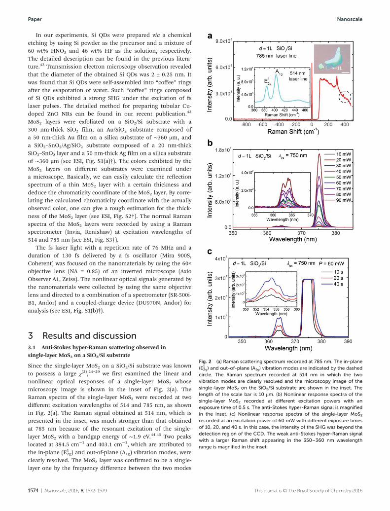
Since the single-layer MoS2 on a SiO2/Si substrate was knownto possess a large χ(2),24–29 we first examined the linear andnonlinear optical responses of a single-layer MoS2 whosemicroscopy image is shown in the inset of Fig. 2(a). TheRaman spectra of the single-layer MoS2 were recorded at twodifferent excitation wavelengths of 514 and 785 nm, as shownin Fig. 2(a). The Raman signal obtained at 514 nm, which ispresented in the inset, was much stronger than that obtainedat 785 nm because of the resonant excitation of the single-layer MoS2 with a bandgap energy of ∼1.9 eV.44,45 Two peakslocated at 384.5 cm−1 and 403.1 cm−1, which are attributed tothe in-plane (E1
2g) and out-of-plane (A1g) vibration modes, wereclearly resolved. The MoS2 layer was confirmed to be a single-layer one by the frequency difference between the two modes
Fig. 2 (a) Raman scattering spectrum recorded at 785 nm. The in-plane(E12g) and out-of-plane (A1g) vibration modes are indicated by the dashedcircle. The Raman spectrum recorded at 514 nm in which the twovibration modes are clearly resolved and the microscopy image of thesingle-layer MoS2 on the SiO2/Si substrate are shown in the inset. Thelength of the scale bar is 10 μm. (b) Nonlinear response spectra of thesingle-layer MoS2 recorded at different excitation powers with anexposure time of 0.5 s. The anti-Stokes hyper-Raman signal is magnifiedin the inset. (c) Nonlinear response spectra of the single-layer MoS2recorded at an excitation power of 60 mW with different exposure timesof 10, 20, and 40 s. In this case, the intensity of the SHG was beyond thedetection region of the CCD. The weak anti-Stokes hyper-Raman signalwith a larger Raman shift appearing in the 350–360 nm wavelengthrange is magnified in the inset.
which is estimated to be 18.6 cm−1.46 No anti-Stokes Ramanscattering was observed in the Raman spectra.
In Fig. 2(b), we present the nonlinear response spectra ofthe single-layer MoS2 recorded by using a fs laser light at750 nm. The exposure time of the CCD, which corresponds tothe integration time of the nonlinear optical signals, waschosen to be 0.5 s. Apart from the strong second harmonic(SH) observed at 375 nm, one can see a nonlinear signal com-posed of two peaks appearing at the short-wavelength side ofthe SH (see the inset of Fig. 2(b)). They are attributed to theanti-Stokes hyper-Raman scattering related to two vibrationmodes with Raman shifts of about 793 cm−1 and 923 cm−1,respectively. These two modes are not found in the normalRaman spectrum of MoS2.
47 In contrast to the normal Ramanscattering, Stokes hyper-Raman scattering was not observed inthe nonlinear response spectra of the single-layer MoS2. Earlyin 2000, Nayfeh et al. also observed a strong anti-Stokeshyper-Raman scattering in the microcrystalline films com-posed of ultrasmall Si nanoparticles which exhibited extremelystrong SHG.20 In their case, the intensity of the anti-Stokeshyper-Raman scattering was even stronger than that of the SH.
In order to resolve more vibration modes in the nonlinearresponse spectra, we increased the integration time from 10 to40 s, as shown in Fig. 2(c). Six vibration modes were clearlyrevealed and their Raman shifts were estimated to be772 cm−1, 888 cm−1, 1378 cm−1, 1492 cm−1, 1594 cm−1 and1667 cm−1, respectively (see ESI, Fig. S4† for the details ofextracting the Raman shifts of these vibration modes).
In Fig. 1(b), it can be seen that the transition rate from theexcited state to the virtual state should be larger than thedecay rate of the excited state to the ground state in order toobserve the anti-Stokes hyper Raman scattering. In this case,the hyper-Rayleigh scattering, which corresponds to SHG, isalso strong because of the large transition rate from theexcited state to the virtual state. For this reason, an enhance-ment in hyper-Raman scattering is also accompanied by anenhancement in SHG, as shown in Fig. 2(c) where the inte-gration time for the nonlinear signals is increased. In otherwords, any method which can be employed to enhance SHGwill also benefit the enhancement in hyper-Raman scattering.
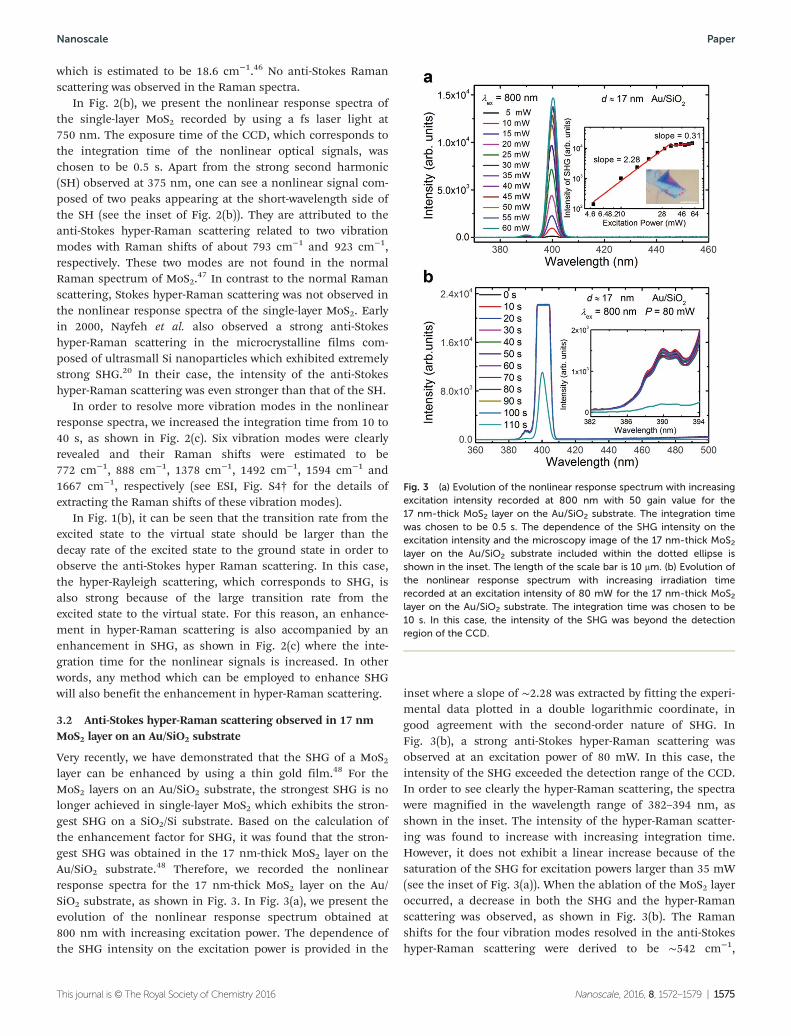
3.2 Anti-Stokes hyper-Raman scattering observed in 17 nmMoS2 layer on an Au/SiO2 substrate
Very recently, we have demonstrated that the SHG of a MoS2layer can be enhanced by using a thin gold film.48 For theMoS2 layers on an Au/SiO2 substrate, the strongest SHG is nolonger achieved in single-layer MoS2 which exhibits the stron-gest SHG on a SiO2/Si substrate. Based on the calculation ofthe enhancement factor for SHG, it was found that the stron-gest SHG was obtained in the 17 nm-thick MoS2 layer on theAu/SiO2 substrate.48 Therefore, we recorded the nonlinearresponse spectra for the 17 nm-thick MoS2 layer on the Au/SiO2 substrate, as shown in Fig. 3. In Fig. 3(a), we present theevolution of the nonlinear response spectrum obtained at800 nm with increasing excitation power. The dependence ofthe SHG intensity on the excitation power is provided in the
inset where a slope of ∼2.28 was extracted by fitting the experi-mental data plotted in a double logarithmic coordinate, ingood agreement with the second-order nature of SHG. InFig. 3(b), a strong anti-Stokes hyper-Raman scattering wasobserved at an excitation power of 80 mW. In this case, theintensity of the SHG exceeded the detection range of the CCD.In order to see clearly the hyper-Raman scattering, the spectrawere magnified in the wavelength range of 382–394 nm, asshown in the inset. The intensity of the hyper-Raman scatter-ing was found to increase with increasing integration time.However, it does not exhibit a linear increase because of thesaturation of the SHG for excitation powers larger than 35 mW(see the inset of Fig. 3(a)). When the ablation of the MoS2 layeroccurred, a decrease in both the SHG and the hyper-Ramanscattering was observed, as shown in Fig. 3(b). The Ramanshifts for the four vibration modes resolved in the anti-Stokeshyper-Raman scattering were derived to be ∼542 cm−1,
Fig. 3 (a) Evolution of the nonlinear response spectrum with increasingexcitation intensity recorded at 800 nm with 50 gain value for the17 nm-thick MoS2 layer on the Au/SiO2 substrate. The integration timewas chosen to be 0.5 s. The dependence of the SHG intensity on theexcitation intensity and the microscopy image of the 17 nm-thick MoS2layer on the Au/SiO2 substrate included within the dotted ellipse isshown in the inset. The length of the scale bar is 10 μm. (b) Evolution ofthe nonlinear response spectrum with increasing irradiation timerecorded at an excitation intensity of 80 mW for the 17 nm-thick MoS2layer on the Au/SiO2 substrate. The integration time was chosen to be10 s. In this case, the intensity of the SHG was beyond the detectionregion of the CCD.
∼655 cm−1, ∼761 cm−1 and ∼846 cm−1 (see ESI, Fig. S4 andTables S1 and S2† for the details of extracting the Ramanshifts of these vibration modes). These four vibration modesare also not found in the normal Raman spectrum of MoS2.
47
In addition, it is noticed that the vibration modes observed inthe 17 nm-thick MoS2 layer on the Au/SiO2 substrate aredifferent from those observed in the single-layer MoS2 on theSiO2/Si substrate. Apart from the difference in thickness, thisbehavior implies that the enhancement in hyper-Ramanscattering provided by the thin gold film is selective. Moreexperiments are needed to clarify this issue.
3.3 Stokes hyper-Raman scattering observed in the ablationof MoS2 layers
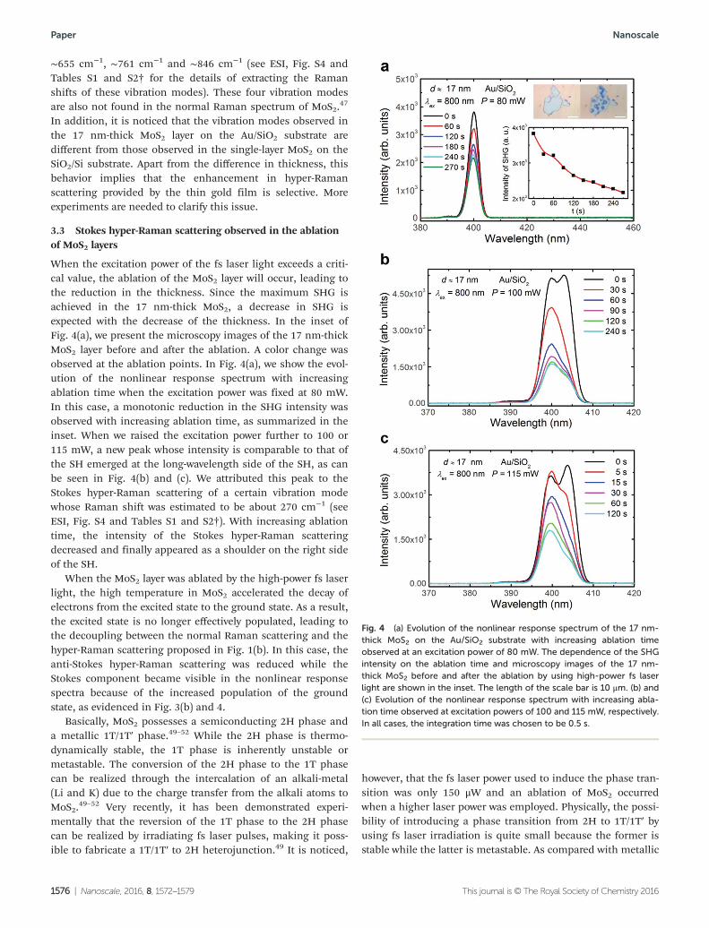
When the excitation power of the fs laser light exceeds a criti-cal value, the ablation of the MoS2 layer will occur, leading tothe reduction in the thickness. Since the maximum SHG isachieved in the 17 nm-thick MoS2, a decrease in SHG isexpected with the decrease of the thickness. In the inset ofFig. 4(a), we present the microscopy images of the 17 nm-thickMoS2 layer before and after the ablation. A color change wasobserved at the ablation points. In Fig. 4(a), we show the evol-ution of the nonlinear response spectrum with increasingablation time when the excitation power was fixed at 80 mW.In this case, a monotonic reduction in the SHG intensity wasobserved with increasing ablation time, as summarized in theinset. When we raised the excitation power further to 100 or115 mW, a new peak whose intensity is comparable to that ofthe SH emerged at the long-wavelength side of the SH, as canbe seen in Fig. 4(b) and (c). We attributed this peak to theStokes hyper-Raman scattering of a certain vibration modewhose Raman shift was estimated to be about 270 cm−1 (seeESI, Fig. S4 and Tables S1 and S2†). With increasing ablationtime, the intensity of the Stokes hyper-Raman scatteringdecreased and finally appeared as a shoulder on the right sideof the SH.
When the MoS2 layer was ablated by the high-power fs laserlight, the high temperature in MoS2 accelerated the decay ofelectrons from the excited state to the ground state. As a result,the excited state is no longer effectively populated, leading tothe decoupling between the normal Raman scattering and thehyper-Raman scattering proposed in Fig. 1(b). In this case, theanti-Stokes hyper-Raman scattering was reduced while theStokes component became visible in the nonlinear responsespectra because of the increased population of the groundstate, as evidenced in Fig. 3(b) and 4.
Basically, MoS2 possesses a semiconducting 2H phase anda metallic 1T/1T′ phase.49–52 While the 2H phase is thermo-dynamically stable, the 1T phase is inherently unstable ormetastable. The conversion of the 2H phase to the 1T phasecan be realized through the intercalation of an alkali-metal(Li and K) due to the charge transfer from the alkali atoms toMoS2.
49–52 Very recently, it has been demonstrated experi-mentally that the reversion of the 1T phase to the 2H phasecan be realized by irradiating fs laser pulses, making it poss-ible to fabricate a 1T/1T′ to 2H heterojunction.49 It is noticed,
however, that the fs laser power used to induce the phase tran-sition was only 150 μW and an ablation of MoS2 occurredwhen a higher laser power was employed. Physically, the possi-bility of introducing a phase transition from 2H to 1T/1T′ byusing fs laser irradiation is quite small because the former isstable while the latter is metastable. As compared with metallic
Fig. 4 (a) Evolution of the nonlinear response spectrum of the 17 nm-thick MoS2 on the Au/SiO2 substrate with increasing ablation timeobserved at an excitation power of 80 mW. The dependence of the SHGintensity on the ablation time and microscopy images of the 17 nm-thick MoS2 before and after the ablation by using high-power fs laserlight are shown in the inset. The length of the scale bar is 10 μm. (b) and(c) Evolution of the nonlinear response spectrum with increasing abla-tion time observed at excitation powers of 100 and 115 mW, respectively.In all cases, the integration time was chosen to be 0.5 s.
1T/1T′-MoS2, the absorption of laser energy by semiconducting2H-MoS2 is much smaller. Consequently, the fs laser power weused was almost three orders of magnitude larger than thatreported for inducing the 1T/1T′ to 2H phase transition. Inorder to confirm that the change in the SHG intensity and filmcolor was caused by ablation rather than phase transition, werecorded the Raman scattering spectra for the un-ablated andablated areas and found no change in the Raman scatteringpeaks (see ESI, Fig. S3b†). This result indicates that theirradiation of fs laser pulses results in the ablation of MoS2rather than the 2H to 1T/1T′ phase transition.
3.4 Stokes hyper-Raman scattering observed in the case ofdefocusing
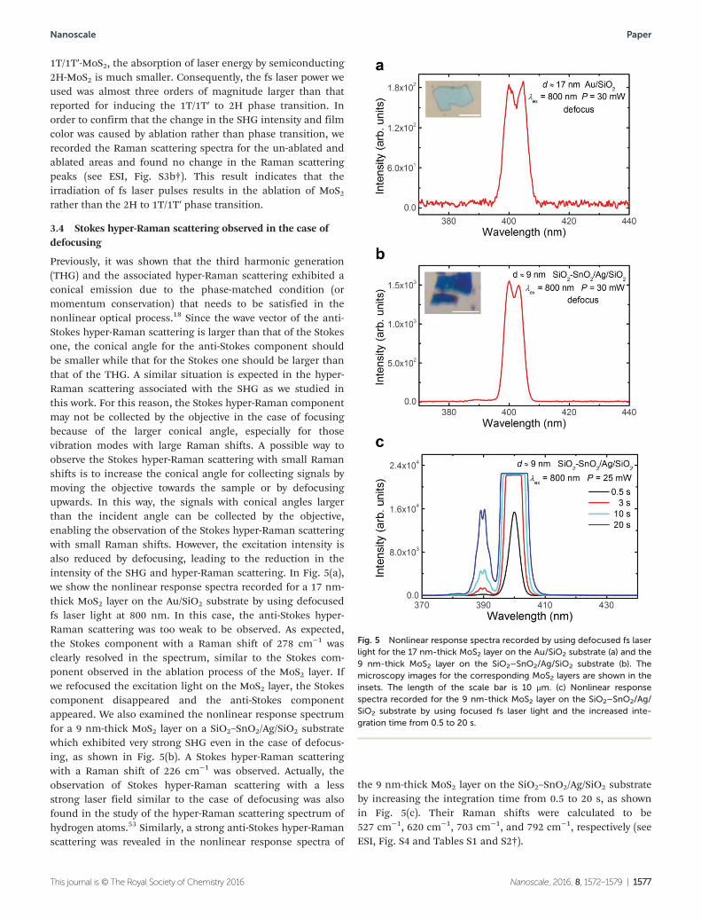
Previously, it was shown that the third harmonic generation(THG) and the associated hyper-Raman scattering exhibited aconical emission due to the phase-matched condition (ormomentum conservation) that needs to be satisfied in thenonlinear optical process.18 Since the wave vector of the anti-Stokes hyper-Raman scattering is larger than that of the Stokesone, the conical angle for the anti-Stokes component shouldbe smaller while that for the Stokes one should be larger thanthat of the THG. A similar situation is expected in the hyper-Raman scattering associated with the SHG as we studied inthis work. For this reason, the Stokes hyper-Raman componentmay not be collected by the objective in the case of focusingbecause of the larger conical angle, especially for thosevibration modes with large Raman shifts. A possible way toobserve the Stokes hyper-Raman scattering with small Ramanshifts is to increase the conical angle for collecting signals bymoving the objective towards the sample or by defocusingupwards. In this way, the signals with conical angles largerthan the incident angle can be collected by the objective,enabling the observation of the Stokes hyper-Raman scatteringwith small Raman shifts. However, the excitation intensity isalso reduced by defocusing, leading to the reduction in theintensity of the SHG and hyper-Raman scattering. In Fig. 5(a),we show the nonlinear response spectra recorded for a 17 nm-thick MoS2 layer on the Au/SiO2 substrate by using defocusedfs laser light at 800 nm. In this case, the anti-Stokes hyper-Raman scattering was too weak to be observed. As expected,the Stokes component with a Raman shift of 278 cm−1 wasclearly resolved in the spectrum, similar to the Stokes com-ponent observed in the ablation process of the MoS2 layer. Ifwe refocused the excitation light on the MoS2 layer, the Stokescomponent disappeared and the anti-Stokes componentappeared. We also examined the nonlinear response spectrumfor a 9 nm-thick MoS2 layer on a SiO2–SnO2/Ag/SiO2 substratewhich exhibited very strong SHG even in the case of defocus-ing, as shown in Fig. 5(b). A Stokes hyper-Raman scatteringwith a Raman shift of 226 cm−1 was observed. Actually, theobservation of Stokes hyper-Raman scattering with a lessstrong laser field similar to the case of defocusing was alsofound in the study of the hyper-Raman scattering spectrum ofhydrogen atoms.53 Similarly, a strong anti-Stokes hyper-Ramanscattering was revealed in the nonlinear response spectra of
the 9 nm-thick MoS2 layer on the SiO2–SnO2/Ag/SiO2 substrateby increasing the integration time from 0.5 to 20 s, as shownin Fig. 5(c). Their Raman shifts were calculated to be527 cm−1, 620 cm−1, 703 cm−1, and 792 cm−1, respectively (seeESI, Fig. S4 and Tables S1 and S2†).
Fig. 5 Nonlinear response spectra recorded by using defocused fs laserlight for the 17 nm-thick MoS2 layer on the Au/SiO2 substrate (a) and the9 nm-thick MoS2 layer on the SiO2–SnO2/Ag/SiO2 substrate (b). Themicroscopy images for the corresponding MoS2 layers are shown in theinsets. The length of the scale bar is 10 μm. (c) Nonlinear responsespectra recorded for the 9 nm-thick MoS2 layer on the SiO2–SnO2/Ag/SiO2 substrate by using focused fs laser light and the increased inte-gration time from 0.5 to 20 s.
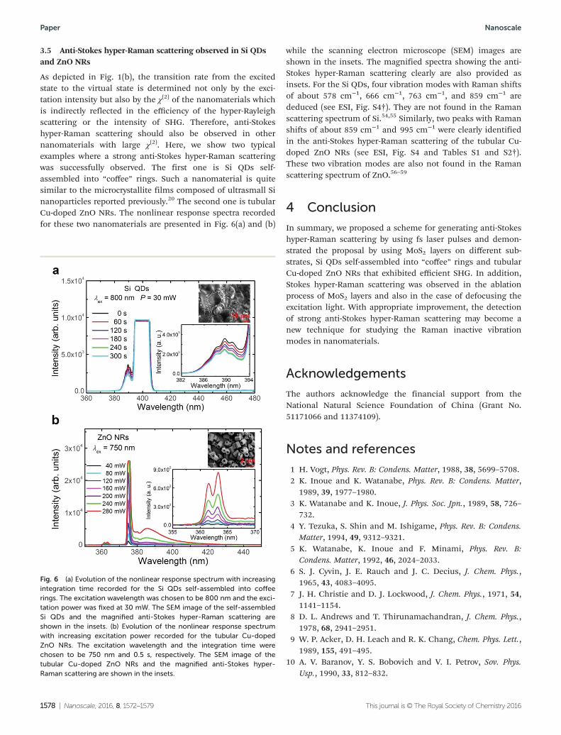
3.5 Anti-Stokes hyper-Raman scattering observed in Si QDsand ZnO NRs
As depicted in Fig. 1(b), the transition rate from the excitedstate to the virtual state is determined not only by the exci-tation intensity but also by the χ(2) of the nanomaterials whichis indirectly reflected in the efficiency of the hyper-Rayleighscattering or the intensity of SHG. Therefore, anti-Stokeshyper-Raman scattering should also be observed in othernanomaterials with large χ(2). Here, we show two typicalexamples where a strong anti-Stokes hyper-Raman scatteringwas successfully observed. The first one is Si QDs self-assembled into “coffee” rings. Such a nanomaterial is quitesimilar to the microcrystallite films composed of ultrasmall Sinanoparticles reported previously.20 The second one is tubularCu-doped ZnO NRs. The nonlinear response spectra recordedfor these two nanomaterials are presented in Fig. 6(a) and (b)
while the scanning electron microscope (SEM) images areshown in the insets. The magnified spectra showing the anti-Stokes hyper-Raman scattering clearly are also provided asinsets. For the Si QDs, four vibration modes with Raman shiftsof about 578 cm−1, 666 cm−1, 763 cm−1, and 859 cm−1 arededuced (see ESI, Fig. S4†). They are not found in the Ramanscattering spectrum of Si.54,55 Similarly, two peaks with Ramanshifts of about 859 cm−1 and 995 cm−1 were clearly identifiedin the anti-Stokes hyper-Raman scattering of the tubular Cu-doped ZnO NRs (see ESI, Fig. S4 and Tables S1 and S2†).These two vibration modes are also not found in the Ramanscattering spectrum of ZnO.56–59
4 Conclusion
In summary, we proposed a scheme for generating anti-Stokeshyper-Raman scattering by using fs laser pulses and demon-strated the proposal by using MoS2 layers on different sub-strates, Si QDs self-assembled into “coffee” rings and tubularCu-doped ZnO NRs that exhibited efficient SHG. In addition,Stokes hyper-Raman scattering was observed in the ablationprocess of MoS2 layers and also in the case of defocusing theexcitation light. With appropriate improvement, the detectionof strong anti-Stokes hyper-Raman scattering may become anew technique for studying the Raman inactive vibrationmodes in nanomaterials.
Acknowledgements
The authors acknowledge the financial support from theNational Natural Science Foundation of China (Grant No.51171066 and 11374109).
Notes and references
1 H. Vogt, Phys. Rev. B: Condens. Matter, 1988, 38, 5699–5708.2 K. Inoue and K. Watanabe, Phys. Rev. B: Condens. Matter,
1989, 39, 1977–1980.3 K. Watanabe and K. Inoue, J. Phys. Soc. Jpn., 1989, 58, 726–
732.4 Y. Tezuka, S. Shin and M. Ishigame, Phys. Rev. B: Condens.
Matter, 1994, 49, 9312–9321.5 K. Watanabe, K. Inoue and F. Minami, Phys. Rev. B:
Condens. Matter, 1992, 46, 2024–2033.6 S. J. Cyvin, J. E. Rauch and J. C. Decius, J. Chem. Phys.,
1965, 43, 4083–4095.7 J. H. Christie and D. J. Lockwood, J. Chem. Phys., 1971, 54,
1141–1154.8 D. L. Andrews and T. Thirunamachandran, J. Chem. Phys.,
1978, 68, 2941–2951.9 W. P. Acker, D. H. Leach and R. K. Chang, Chem. Phys. Lett.,
1989, 155, 491–495.10 A. V. Baranov, Y. S. Bobovich and V. I. Petrov, Sov. Phys.
Usp., 1990, 33, 812–832.
Fig. 6 (a) Evolution of the nonlinear response spectrum with increasingintegration time recorded for the Si QDs self-assembled into coffeerings. The excitation wavelength was chosen to be 800 nm and the exci-tation power was fixed at 30 mW. The SEM image of the self-assembledSi QDs and the magnified anti-Stokes hyper-Raman scattering areshown in the insets. (b) Evolution of the nonlinear response spectrumwith increasing excitation power recorded for the tubular Cu-dopedZnO NRs. The excitation wavelength and the integration time werechosen to be 750 nm and 0.5 s, respectively. The SEM image of thetubular Cu-doped ZnO NRs and the magnified anti-Stokes hyper-Raman scattering are shown in the insets.
11 H. Vogt and G. Neumann, Phys. Status Solidi B, 1979, 92,57–63.
12 H. Vogt, J. A. Sanjurjo and G. Rossbroich, Phys. Rev. B:Condens. Matter, 1982, 26, 5904–5910.
13 A. V. Baranov, K. Inoue, K. Toba, A. Yamanaka, V. I. Petrovand A. V. Fedorov, Phys. Rev. B: Condens. Matter, 1996, 53,R1721–R1724.
14 K. Inoue, A. Yamanaka, K. Toba, A. V. Baranov,A. A. Onushchenko and A. V. Fedorov, Phys. Rev. B:Condens. Matter, 1996, 54, R8321–R8324.
15 M. Mizuno, H. Hamaguchi and T. Tahara, J. Phys. Chem. A,2002, 106, 3599–3604.
16 J. Kneipp, H. Kneipp and K. Kneipp, Proc. Natl. Acad.Sci. U. S. A., 2006, 103, 17149–17153.
17 S. O. Konorov, D. A. Akimov, A. A. Ivanov, M. V. Alfimovand A. M. Zheltikov, J. Exp. Theor. Phys., 2004, 99, 19–27.
18 D. Homoelle, K. D. Moll, A. L. Gaeta and R. W. Boyd, Phys.Rev. A, 2005, 72, 011802(R).
19 A. Fontes, K. Ajito, A. A. R. Neves, W. L. Moreira, A. A. deThomaz, L. C. Barbosa, A. M. de Paula and C. L. Cesar,Phys. Rev. E: Stat. Phys., Plasmas, Fluids, Relat. Interdiscip.Top., 2005, 72, 012903.
20 M. H. Nayfeh, O. Akcakir, G. Belomoin, N. Barry,J. Therrien and E. Gratton, Appl. Phys. Lett., 2000, 77, 4086–4088.
21 A. Zumbusch, G. R. Holtom and X. S. Xie, Phys. Rev. Lett.,1999, 82, 4142–4145.
22 C. Hubert, L. Billot, P.-M. Adam, R. Bachelot, P. Royer,J. Grand, D. Gindre, K. D. Dorkenoo and A. Fort, Appl. Phys.Lett., 2007, 90, 181105.
23 G. Liu, H. Deng, G. Li, L. Chen, Q. Dai, S. Lan and S. Tie,Plasmonics, 2014, 9, 1471–1480.
24 N. Kumar, S. Najmaei, Q. Cui, F. Ceballos, P. M. Ajayan,J. Lou and H. Zhao, Phys. Rev. B: Condens. Matter, 2013, 87,161403(R).
25 L. M. Malard, T. V. Alencar, A. P. M. Barboza, K. F. Mak andA. M. dePaula, Phys. Rev. B: Condens. Matter, 2013, 87,201401(R).
26 Y. Li, Y. Rao, K. F. Mak, Y. You, S. Wang, C. R. Dean andT. F. Heinz, Nano Lett., 2013, 13, 3329–3333.
27 W. T. Hsu, Z. A. Zhao, L. J. Li, C. H. Chen, M. H. Chiu,P. S. Chang, Y. C. Chou and W. H. Chang, ACS Nano, 2014,8, 2951–2958.
28 X. B. Yin, Z. L. Ye, D. A. Chenet, Y. Ye, K. O’Brien,J. C. Hone and X. Zhang, Science, 2014, 344, 488–490.
29 R. Wang, H. C. Chien, J. Kumar, N. Kumar, H. Y. Chiu andH. Zhao, Appl. Mater. Interfaces, 2014, 6, 314–318.
30 D. Maikhuri, S. P. Purohit and K. C. Mathur, AIP Adv., 2015,5, 047115.
31 S. Sauvage, T. Brunhes, P. Boucaud, A. Lemaitre,J.-M. Gerard, F. Glotin, R. Prazeres and J.-M. Ortega, Phys.Status Solidi B, 2001, 224, 595–598.
32 L. Liu, S. B. Kumar, Y. Ouyang and J. Guo, IEEE Trans.Electron Devices, 2011, 58, 3042–3047.
33 Y. Yoon, K. Ganapathi and S. Salahuddin, Nano Lett., 2011,11, 3768–3773.
34 H. Wang, L. Yu, Y.-H. Lee, Y. Shi, A. Hsu, M. Chin, L.-J. Li,M. Dubey, J. Kong and T. Palacios, Nano Lett., 2012, 12,4674–4680.
35 B. Radisavljevic, M. B. Whitwick and A. Kis, ACS Nano,2011, 5, 9934–9938.
36 S. Bertolazzi, J. Brivio and A. Kis, ACS Nano, 2011, 5, 9703–9709.
37 Q. He, Z. Zeng, Z. Yin, H. Li, S. Wu, X. Huang andH. Zhang, Small, 2012, 8, 2994–2999.
38 J. Pu, Y. Yomogida, K.-K. Liu, L.-J. Li, Y. Iwasa andT. Takenobu, Nano Lett., 2012, 12, 4013–4017.
39 Z. Yin, H. Li, H. Li, L. Jiang, Y. Shi, Y. Sun, G. Lu, Q. Zhang,X. Chen and H. Zhang, ACS Nano, 2012, 6, 74–80.
40 H. S. Lee, S.-W. Min, Y.-G. Chang, P. M. Kyu, T. Nam,H. Kim, J. H. Kim, S. Ryu and S. Im, Nano Lett., 2012, 12,3695–3700.
41 M. Shanmugam, T. Bansal, C. A. Durcan and B. Yu, Appl.Phys. Lett., 2012, 100, 153901.
42 K. Sato, H. Tsuji, K. Hirakuri, N. Fukata and Y. Yamauchi,Chem. Commun., 2009, 3759–3761.
43 X. Wan, X. Liang, C. Zhang, X. Li, W. Liang, H. Xu, S. Lanand S. Tie, Chem. Eng. J., 2015, 272, 58–68.
44 K. F. Mak, C. Lee, J. Hone, J. Shan and T. F. Heinz, Phys.Rev. Lett., 2010, 105, 136805.
45 H. Zeng, J. Dai, W. Yao, D. Xiao and X. Cui, Nat. Nanotech-nol., 2012, 7, 490–493.
46 H. Li, Q. Zhang, C. C. R. Yap, B. K. Tay, T. H. T. Edwin,A. Olivier and D. Baillargeat, Adv. Funct. Mater., 2012, 22,1385–1390.
47 B. C. Windom, W. G. Sawyer and D. W. Hahn, Tribol. Lett.,2011, 42, 301–310.
48 J. Zeng, M. Yuan, W. Yuan, Q. Dai, H. Fan, S. Lan andS. Tie, Nanoscale, 2015, 7, 13547–13553.
49 Y. Guo, D. Sun, B. Ouyang, A. Raja, J. Song, T. F. Heinz andL. E. Brus, Nano Lett., 2015, 15, 5081–5088.
50 X. Fan, P. Xu, D. Zhou, Y. Sun, Y. C. Li, M. A. T. Nguyen,M. Terrones and T. E. Mallouk, Nano Lett., 2015, 15, 5956–5960.
51 M. Chhowalla, D. Voiry, J. Yang, H. S. Shin and K. P. Loh,MRS Bull., 2015, 40, 585–591.
52 G. Gao, Y. Jiao, F. Ma, Y. Jiao, E. Waclawik and A. Du,J. Phys. Chem. C, 2015, 119, 13124–13128.
53 Z. Zhou and J. Yuan, Phys. Rev. A, 2008, 77, 063411.54 M. H. Brodsky, M. Cardona and J. J. Cuomo, Phys. Rev. B:
Solid State, 1977, 16, 3556–3571.55 R. Wang, G. Zhou, Y. Liu, S. Pan, H. Zhang, D. Yu and
Z. Zhang, Phys. Rev. B: Condens. Matter, 2000, 61, 16827–16832.
56 X. Wang, S. Yang, J. Wang, M. Li, X. Jiang, G. Du, X. Liuand R. P. H. Chang, J. Cryst. Growth, 2001, 226, 123–129.
57 F. J. Manjón, B. Marí, J. Serrano and A. H. Romer, J. Appl.Phys., 2005, 97, 053516.
58 N. H. Nickel, F. Friedrich, J. F. Rommeluère and P. Galtier,Appl. Phys. Lett., 2005, 87, 211905.
59 S.-S. Lo and D. Huang, Langmuir, 2010, 26, 6762–6766.