32
* CAD (Computer Aided Design) FOR PRINTED WIRING BOARDS * DESIGN FOR MANUFACTURABILITY ConDnued..
| Date post: | 30-Jun-2018 |
| Category: |
Documents |
| Upload: | trankhuong |
| View: | 215 times |
| Download: | 0 times |
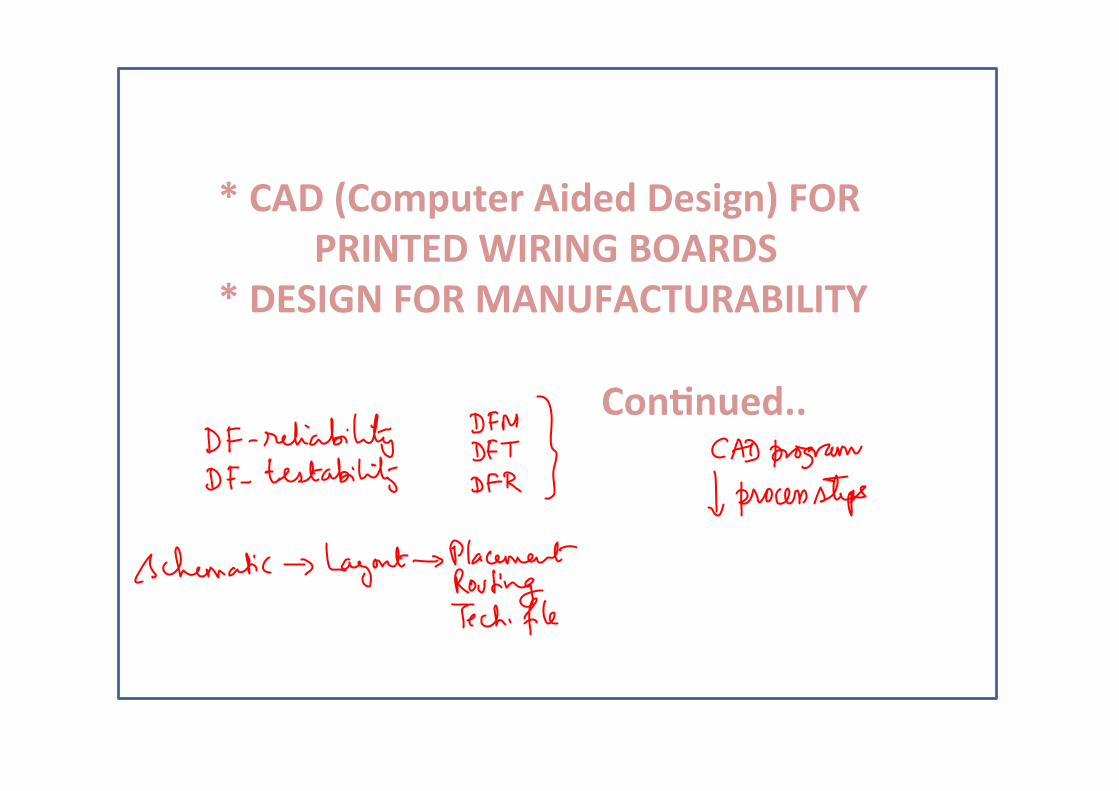
* CAD (Computer Aided Design) FOR PRINTED WIRING BOARDS
* DESIGN FOR MANUFACTURABILITY
ConDnued..

Layout will automatically insert footprints into a board based on the information in the Capture "PCB Footprint" field.

Design rules must be entered into the layout system before the traces can be placed. Design Rules are required in terms of the minimum spacing allowed between electrical items on the design and for assigning minimum values to certain parameters which may be requ i red by the manufac tur ing processes.
To set a board layout finally before rou1ng begins: o Define resource files and the target directory for the design o Select the units of measurement o Create the board outline o Define the layer stack o Set system grids o Specify the component types used in the design o Define the manufacturing technology and complexity o Set spacing rules o Define padstacks o Define vias o Select colour se?ngs for the graphical display of your design

Board Outline and Grid Se?ngs

Spacing rules and Netlist selec1on for rou1ng

Fan out Fan-out is a method for routing surface mount pads where densely packed boards that prohibit routing on surface layers on your board (like BGA array fine pitch with high pin count IC). Fan-out routes surface mount pads to a via so the pad can be routed to other layers like POWER and GND plane. Fan-‐out applica1ons: o Mul1layer boards that include power and ground planes o Densely packed boards that prohibit rou1ng on the surface layers o Boards that include fine-‐pitch components that impede surface rou1ng o Boards that need minimum route exposure

Placing components in Layout Module- a short demo by video

Auto (Routing)
• Rou1ng follows placement • Netlist –key to rou1ng successfully • Set design rules before rou1ng • Different packages have different rou1ng algorithms • Speed is not the key factor, successful comple1on with shorter interconnect lengths is the issue
• Try manual, assisted and fully auto • High-‐density board rou1ng requires 1me, modifica1on of design rules if required and complete understanding of layout

Auto rou1ng: single-‐sided board: a demo

Auto rou1ng: double-‐sided board: a demo


Auto rou1ng: four-‐layer board: a demo

Gerber file genera1on (Tech files)

Example of a Drill Report file

Signal Checks Conductor Width Spacing Annular Ring Drill to Copper Hole Registration Text Features Missing Copper Features Connection Missing Holes Unconnected Lines Rout to Copper
Plane Checks Drill to Copper Annular Ring Spacing Conductor Width Thermal Air gap / Spoke Width Missing Copper Rout to Copper Drill Registration Clearance smaller than hole
Solder Mask Checks Solder Mask Clearance Coverage Rout to Mask Spacing Missing Solder Mask Clearance Exposed Lines Partial Clearances
Silk Screen Checks Silk Screen to Mask Spacing Silk Screen to Copper Spacing Silk Screen to Hole Spacing Silk Screen to Rout Spacing Line Width Text Height Silk Screen Over Copper Text
Drill Checks Hole Size Duplicate Holes Hole Spacing Touching Holes Plane Shorts Holes to Rout Missing Holes
Source: Sierra Circuits
DFM Checklist

(anti-pad)
Thermal relief pads are connected to the plane and isolation pads are not connected to the plane.

A special pattern etched around a via or a plated through-hole to connect it into a power or ground plane. A thermal relief pad is necessary to prevent too much heat being absorbed into the power or ground plane when the board is being soldered.
Via/Pin with thermal Via/Pin without thermal

Thermal reliefs on a PCB are to make it easier to solder and desolder through-hole components when you have a PCB with internal planes, large Cu poured planes or wide conducting traces. Without the relief pattern the plane will act as a heat sink drawing much of the heat away from the lead you are trying to solder or desolder. This could be a cold solder joint or the need to apply excess heat while soldering, resulting in a damage to the board.

Board Design for BGAs
q Solder mask should cover the vias (tenting process) q Solder mask is a material which prevents ‘bridging’ of tracks q Minimizes cross talk between tracks q SMD and NSMD defined vias are both common for BGA pads; reliability is an issue; non solder mask defined pads are better
q High routing density achieved with this design process q HDI interconnect technology is a requirement for BGA/CSPs

q Designers need to be aware of !!
Textbook for this course: ‘Fundamentals of Microsystems Packaging’ by Rao Tummala


m


END of CHAPTER


