Cadmium selenide@sulfide nanoparticle composites: Facile precipitation preparation, characterization, and investigation of their photocatalyst activity Omid Amiri a,b , Masoud Salavati-Niasari a,n , S. Mostafa Hosseinpour-Mashkani c , Ali Rafiei d , Samira Bagheri e a Institute of Nano Science and NanoTechnology, University of Kashan, P.O. Box 87317-51167, Kashan, Iran b Young Researchers and Elite Club, Kashan Branch, Islamic Azad University, Kashan, Iran c Center for Nanoscience and Technology, IST, Jawaharlal Nehru Technological University Hyderabad, Hyderabad-500085, Andhra Pradesh, India d Department of Chemistry, University of Sistan and Baluchestan, Zahedan, Iran e Centre for Research in Nanotechnology & Catalysis (NANOCAT), 3rd Floor, Block A, Institute of Postgraduate Studies (IPS) Building, University of Malaya, Kuala Lumpur-50603, Malaysia article info Keywords: Nanoparticles Semiconductors Photocatalyst activity Core–shell Electron microscopy abstract We report a two-step synthesis and structural characterization of CdSe/CdS core/shell nanoparticles by the precipitation method. Besides, the effects of preparation parameters such as reaction temperature, the speed of the reaction stirrer, and the rate of adding sulfide source on the size, morphology, and photocatalyst activity of CdSe/CdS core–shell nanoparticles were studied by SEM images and degradation of methyl orange (MO) dye test. The structure and composition of the obtained products were characterized by X-ray diffraction (XRD), transmission electron microscopy (TEM), high-resolution field-emission transmission electron microscope (HRTEM), photoluminescence spectroscopy (PL), scan- ning electronic microscopy (SEM), spectra energy dispersive analysis of X-ray (EDS), and ultraviolet–visible (UV–vis) techniques. & 2014 Elsevier Ltd. All rights reserved. 1. Introduction Recently, in the nanomaterial family, characterization and application of semiconductors have received substan- tial attention due to their unique chemical and physical properties. These properties can be exploited and utilized for various applications, including optoelectronic devices, biological probes, and analytical sensors [1–6]. It has been recognized that the quality of semiconductors can affect significantly their potential applications. Therefore, it is of primary importance to develop convenient, low-cost and green methods to synthesize high-quality semiconductors. In particular, ligand protected semiconductors such as CdSe have been increasingly explored as analytical tools in many biological fields since the seminar works from Alivisatos and coworkers [7] and Chan and Nie [8]. The surface atoms of semiconductors usually have fewer adjacent coordinate atoms and more dangling bonds, which can be thought as defects as compared with the bulk atoms. These defects may induce additional electronic states in the band gap, mix with the intrinsic states to a substantial extent, influence the spacing of the energy levels, and lead to debase the optical properties of semi- conductors. An obvious progress toward the preparation of durable semiconductors with high semiconductors is the passivation of their surface with an inorganic shell with Contents lists available at ScienceDirect journal homepage: www.elsevier.com/locate/mssp Materials Science in Semiconductor Processing http://dx.doi.org/10.1016/j.mssp.2014.06.020 1369-8001/& 2014 Elsevier Ltd. All rights reserved. n Corresponding author. Tel.: þ98 361 555 2383; fax: þ98 361 555 29 30. E-mail address: [email protected](M. Salavati-Niasari). Materials Science in Semiconductor Processing 27 (2014) 261–266
Transcript
Contents lists available at ScienceDirect
Materials Science in Semiconductor Processing
Materials Science in Semiconductor Processing 27 (2014) 261–266
http://d1369-80
n CorrE-m
journal homepage: www.elsevier.com/locate/mssp
Cadmium selenide@sulfide nanoparticle composites: Facileprecipitation preparation, characterization, and investigationof their photocatalyst activity
Omid Amiri a,b, Masoud Salavati-Niasari a,n, S. Mostafa Hosseinpour-Mashkani c,Ali Rafiei d, Samira Bagheri e
a Institute of Nano Science and Nano Technology, University of Kashan, P.O. Box 87317-51167, Kashan, Iranb Young Researchers and Elite Club, Kashan Branch, Islamic Azad University, Kashan, Iranc Center for Nanoscience and Technology, IST, Jawaharlal Nehru Technological University Hyderabad, Hyderabad-500085,Andhra Pradesh, Indiad Department of Chemistry, University of Sistan and Baluchestan, Zahedan, Irane Centre for Research in Nanotechnology & Catalysis (NANOCAT), 3rd Floor, Block A, Institute of Postgraduate Studies (IPS) Building,University of Malaya, Kuala Lumpur-50603, Malaysia
We report a two-step synthesis and structural characterization of CdSe/CdS core/shellnanoparticles by the precipitation method. Besides, the effects of preparation parameterssuch as reaction temperature, the speed of the reaction stirrer, and the rate of addingsulfide source on the size, morphology, and photocatalyst activity of CdSe/CdS core–shellnanoparticles were studied by SEM images and degradation of methyl orange (MO) dyetest. The structure and composition of the obtained products were characterized by X-raydiffraction (XRD), transmission electron microscopy (TEM), high-resolution field-emissiontransmission electron microscope (HRTEM), photoluminescence spectroscopy (PL), scan-ning electronic microscopy (SEM), spectra energy dispersive analysis of X-ray (EDS), andultraviolet–visible (UV–vis) techniques.
& 2014 Elsevier Ltd. All rights reserved.
1. Introduction
Recently, in the nanomaterial family, characterizationand application of semiconductors have received substan-tial attention due to their unique chemical and physicalproperties. These properties can be exploited and utilizedfor various applications, including optoelectronic devices,biological probes, and analytical sensors [1–6]. It has beenrecognized that the quality of semiconductors can affectsignificantly their potential applications. Therefore, it is ofprimary importance to develop convenient, low-cost and
: þ98 361 555 29 30.ti-Niasari).
green methods to synthesize high-quality semiconductors.In particular, ligand protected semiconductors such asCdSe have been increasingly explored as analytical toolsin many biological fields since the seminar works fromAlivisatos and coworkers [7] and Chan and Nie [8].The surface atoms of semiconductors usually have feweradjacent coordinate atoms and more dangling bonds,which can be thought as defects as compared with thebulk atoms. These defects may induce additional electronicstates in the band gap, mix with the intrinsic states to asubstantial extent, influence the spacing of the energylevels, and lead to debase the optical properties of semi-conductors. An obvious progress toward the preparation ofdurable semiconductors with high semiconductors is thepassivation of their surface with an inorganic shell with
O. Amiri et al. / Materials Science in Semiconductor Processing 27 (2014) 261–266262
wider band gap. Various II–VI semiconductors have beeninvestigated as shell material for CdSe semiconductors toimprove the QYs and chemical stability [9–14]. Core/shellmaterials Such as CdS/ZnS [15] CdSe/CdS [16] CdSe/ZnSe[17] CdS/Cd(OH)2 [18], and CdS/HgS/CdS [19] consist of acore structural domain covered by a shell domain [20].In comparison to heterogeneous core/shell nanostructures(two different kinds of materials for the core and theshell), the homogeneous core/shell nanostructures(the same material for both the core and the shell) aremuch more difficult to prepare [20]. There are quite a widerange of available methods to prepare core/shell typenanoparticles during the past several years [15–17]. Sev-eral methods have been used for the preparation ofCdSe@CdSe core shells, Including sonochemistry, sol-vothermal and reflux [21–23]. The new preparing methoddescribed here is inexpensive. The method consists ofsimple steps, allowing for low cost processing.
Semiconductors have beenwidely used as photocatalystsfor environmental problems in recent years. The normalpractical applications of the semiconductors for widespreadenvironmental solutions were found in the fields of waterpurification, waste water treatment, hazardous waste con-trol, air purification, water disinfection and the like. Indus-trial waste waters containing toxic organic dyes have seriousproblems to the environment [24]. About 1–20% of the totalworld production of dyes is lost during the dyeing processand is released into the environment as textile effluents[25,26]. It must be noted that organic dyes can produce toxicsubstances through oxidation, hydrolysis or other chemicalreactions occurring in the wastewater phase [27–29]. Thedecolorization of dyes in the industrial wastewater hasreceived increasing attention. Herein, we report a simplebut effective method for direct preparation of core/shellnanoparticles CdSe/CdS using cadmium acetate, thioaceta-mide and selenium tetrachloride as precursors in presenceof sodium dodecyl sulfate as the surfactant by the precipita-tion method. Preliminary tests on these nanoparticles fordegradation of methyl orange (MO) dye were positive,which indicates CdSe/CdS core/shell nanoparticles are sui-table materials for photocatalytic applications.
Table 1Reaction conditions for CdSe/CdS core/shell nanoparticles.
X-ray diffraction (XRD) patterns were recorded by aPhilips-X’Pert Pro, X-ray diffractometer using Ni-filteredCu Kα radiation at scan range of 10o2θo80. Scanningelectron microscopy (SEM) images were obtained on LEO-1455VP equipped with an energy dispersive X-ray spectro-scopy. Transmission electron microscope (TEM) imageswere obtained on a Philips EM208S transmission electronmicroscope with an accelerating voltage of 100 kV. Roomtemperature photoluminescence (Pl) properties were stu-died on a Perkin–Elmer (LS 55) fluorescence spectrophot-ometer. The energy dispersive spectrometry (EDS) analysiswas studied by XL30, Philips microscope. UV–vis diffusereflectance spectroscopy analysis (UV–vis) was carried outusing Shimadzu UV–vis scanning spectrometer.
2.2. Synthesis of CdSe core nanoparticles
CdSe nanostructures were prepared by the followingexperimental sequence: in a typical procedure, 700 mg ofCd(CH3COO)2 �2H2O was dissolved in 50 ml of distilledwater. A stoichiometric amount of sodium dodecyl sulfatedissolved in an equal volume of distilled water was addeddrop-wise into the above solution. Finally, 40 ml of thesolution containing 580 mg of SeCl4 was added drop wiseto it under magnetic stirring. This solution was stirreduntil a homogeneous solution was obtained. The finalsolution was heated at 70 1C for 1 h under stirring. As aresult, a red precipitate was finally produced.
2.3. Overcoating with CdS
In a typical experiment, 700 mg of Cd(CH3COO)2 �2H2Owas dissolved in aqueous solution contain CdSe nanoparti-cles (40 ml) under stirring; after 30 min stirring, a solutioncontaining Thioacetamide (TAA) was added. After that, thecontent was magnetically stirred at various conditions.Upon Cd precursor and S precursor addition, the solutioncolor changed from red to lemon-yellow. Finally, the as-produced precipitate was filtered, washed by de-ionizedwater and absolute ethanol and dried in vacuum. Table 1shows the conditions of reactions in details.
2.4. Photocatalytic studies
The photocatalytic activity of the CdSe/CdS core–shellnanoparticles was studied by the degradation of MO dye asa target pollutant. The photocatalytic reaction systemincluded a 500 ml cylindrical glass reactor equipped witha light source, which was located axially and held in aquartz immersion tube. A circulating water jacket wasemployed to cool the radiation source and cancel theinfrared radiation, thus preventing any heating of thesuspension. In a typical photocatalytic test performed atroom temperature, 0.3 g of photocatalyst nanopartiles wasadded into 20 ml MO aqueous solution, and then dispersedby stirring for 30 min. Later, a 250 W halogen lamp wasswitched on the suspension. A 250 W high-pressure mer-cury lamp (GYZ-250) was fixed at a distance of 30 cmabove the surface solution. After 90 min, 5 ml of thesuspension was sampled. Then, the changes of MO con-centration were monitored using a UV–vis spectrophot-ometer (U 3010, Hitachi, Japan).
Fig. 2. (a) UV–vis diffuse reflectance spectra of CdSe nanoparticles andCdSe/CdS core–shell nanoparticles. (b) Room temperature PL spectra of:CdS (red line) CdSe/CdS core–shell nanoparticles (blue line). (For inter-pretation of the references to color in this figure legend, the reader isreferred to the web version of this article.)
O. Amiri et al. / Materials Science in Semiconductor Processing 27 (2014) 261–266 263
3. Results and discussion
The crystal structure and phase composition of theCdSe nanoparticles and CdSe/CdS core/shell nanoparticlesof the products were characterized by powder X-raydiffraction patterns, as shown in Fig. 1a and b, respectively.The diffraction peaks observed in Fig. 1a can be indexed topure cubic phase cadmium selenide (space group P63mc,JCPDS No. 75-0581). Fig. 1b shows the X-ray diffractionpatterns of as-prepared CdSe/CdS core/shell. According toFig. 1b, no peaks from other phases or impurities can bedetected. In addition, all the diffraction peaks can bereadily indexed as the cubic structure CdSe/CdS core/shellnanoparticles, which is in agreement with the literature(JCPDS No. 77-0245). The UV–vis absorption spectra of theCdSe/CdS core–shell and CdSe nanoparticles wererecorded as shown in Fig. 2a. Utilizing Tauc's formula,the optical band gap (Eg) can be experimentally obtainedfrom the absorption coefficient according to the followingEq. (1):
ðαhυÞ ¼ Aðhυ�EgÞn ð1Þ
where α is the absorption coefficient, A is constant and ndepends on the type of electronic transition and can beany value between 1/2 and 3 [15]. The photoluminescence(PL) of the prepared CdS and CdSe/CdS core shells areshown in Fig. 2b. It can be seen that the photolumines-cence intensity of CdSe/CdS core shells, compared to CdSnanoparticles, increased and the emission peak (520 nm)was red shifted for 60 nm. This is because the growth of aCdS shells, as observed in XRD and HRTEM images,suppressed deep trap emissions by passivating most ofthe vacancies and trapping sites on the CdSe crystallitesurface, which resulted in photoluminescence dominatedby band edge recombination. The effects of the reactiontemperature, the speed of reaction stirrer, and the rate ofadding sulfide source on the morphology of CdSe/CdScore–shell nanoparticles prepared using precipitationmethod have been investigated by SEM images. SEMimages of samples 1–3 prepared at 70 1C by reaction stirrerwith the speed of 400 rpm are shown in Fig. 3a–c,respectively. It is clear that the best nanoparticle was
obtained at 1 ml/min rate of adding the sulfide source(Fig. 3b), and further increase of this rate did not produceseparated particles. It can be concluded that when theconcentration of thioacetamide is increased, the concen-tration of S2� also increases. These free S2� ions resultedfrom the excessive number of thioacetamide moleculesbind to the surface of the CdSe/CdS core–shell nanoparti-cles. In addition, hydrogen as well as and S–S bonds areformed between thioacetamide molecules. The CdSe/CdScore–shell nanoparticles cross-link together via hydrogenbonds and S–S bond interactions. Thus, the optimumadding rate is 1 ml/min in the current experiment (sampleno. 2). TEM and HRTEM images were taken to characterizethe morphology and size distribution of semiconductors.The TEM and HRTEM images of CdSe nanaoparticles ascores and CdSe/CdS core–shell nanoparticles are shown inFig. 4. According to Fig. 4a, the synthesized CdSe nanao-particles were monodispersed with an average diameter of
Fig. 3. SEM images of CdSe/CdS core–shell nanoparticles (a) sample 1, (b) sample 2, (c) sample 3.
Fig. 4. TEM images of CdSe (a) and subsequent CdSe/CdS core/shell nanoparticles (b). (c) and (d) Are the corresponding HRTEM images of (a) and (b),respectively.
O. Amiri et al. / Materials Science in Semiconductor Processing 27 (2014) 261–266264
10 nm. Fig. 4b, the TEM image of the as-synthesized CdSe/CdS core–shell nanoparticles, shows they have a sphericalshape. Based on the synthesis process, the sharp contrastin the TEM image between the core and shell region is due
to the difference between electron penetration efficiencyon CdSe and CdS. Fig. 4c and d shows the HRTEM images ofCdSe and CdSe/CdS core–shell nanoparticles, respectively.The HRTEM image of the CdSe nanoparticles is shown in
Fig. 5. SEM images of CdSe/CdS core–shell nanoparticles (a) sample 4, (b) sample 5.
Fig. 6. SEM images of CdSe/CdS core–shell nanoparticles (a) sample 6, (b) sample 7, (c) sample 8.
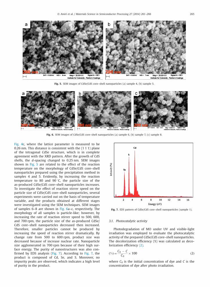
Fig. 7. EDS pattern of CdSe/CdS core–shell nanoparticles (sample 1).
O. Amiri et al. / Materials Science in Semiconductor Processing 27 (2014) 261–266 265
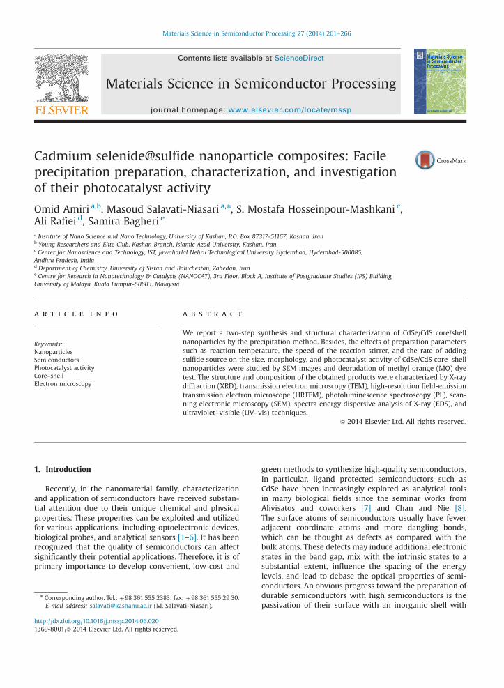
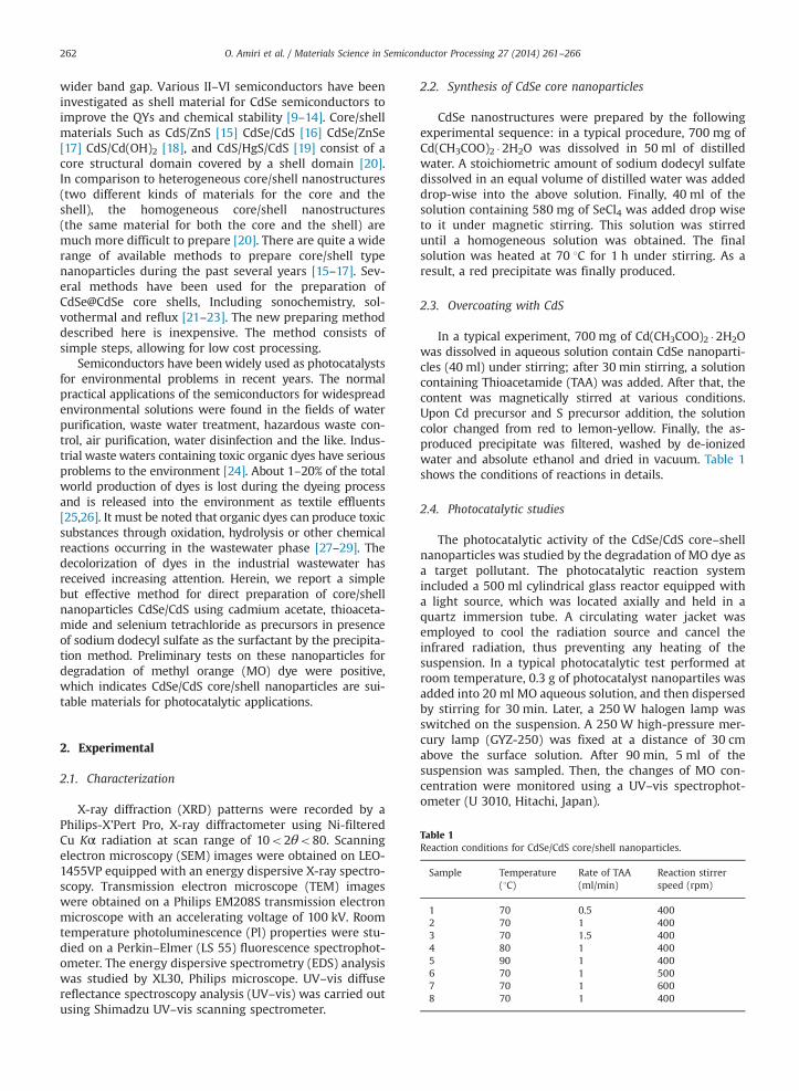
Fig. 4c, where the lattice parameter is measured to be0.26 nm. This distance is consistent with the (1 1 1) planeof the tetragonal CdSe structure, which is in completeagreement with the XRD pattern. After the growth of CdSshells, the d-spacing changed to 0.25 nm. SEM imagesshown in Fig. 5 are related to the effect of the reactiontemperature on the morphology of CdSe/CdS core–shellnanoparticles prepared using the precipitation method insamples 4 and 5. Evidently, by increasing the reactiontemperature to 80 and 90 1C, the particle size of theas-produced CdSe/CdS core–shell nanoparticles increases.To investigate the effect of reaction stirrer speed on theparticle size of CdSe/CdS core–shell nanoparticles, severalexperiments were carried out on the basis of temperaturevariable, and the products obtained at different stageswere investigated using the SEM techniques. SEM imagesof samples 6–8 are shown in Fig. 6a–c, respectively. Themorphology of all samples is particle-like; however, byincreasing the rate of reaction stirrer speed to 500, 600,and 700 rpm, the particle size of the as-produced CdSe/CdS core–shell nanoparticles decreased then increased.Therefore, smaller particles cannot be produced byincreasing the speed of reaction stirrer dramatically. Bychange rate from 500 to 600 rpm, product size wasdecreased because of increase nuclear rate. Nanoparticlesize agglomerated in 700 rpm because of their high sur-face energy. The purity of nanostructures was also con-firmed by EDS analysis (Fig. 7). According to Fig. 7, theproduct is composed of Cd, Se, and S. Moreover, noimpurity peaks are observed, which indicates a high levelof purity in the product.
3.1. Photocatalytic activity
Photodegradation of MO under UV and visible-lightirradiation was employed to evaluate the photocatalyticactivity of the prepared CdSe/CdS core–shell nanoparticles.The decolorization efficiency (%) was calculated as deco-lorization efficiency (2).
ð%Þ ¼ C0 � CC0
� 100 ð2Þ
where C0 is the initial concentration of dye and C is theconcentration of dye after photo irradiation.
Fig. 8. Effect of different CdSe/CdS core–shell nanoparticles samples ondegradation rates of MO.
O. Amiri et al. / Materials Science in Semiconductor Processing 27 (2014) 261–266266
Fig. 8 shows the effect of reaction temperature, stirrerspeed, and rate of adding sulfide source in the absorbanceprofiles of MO solution in presence of CdSe/CdS core–shellnanoparticles under UV irradiation. It seems the increasein rate of adding sulfide results in an increase in photo-catalytic activity. Moreover, photocatalytic activity of sam-ple no. 3 decreases because the increase in rate of addingTAA leads to agglomeration of nanoparticles. Furthermore,with by increasing the reaction temperature up to 80 1C,photocatalytic activity increases. The increase in reactiontemperature up to 90 1C results in a decrease in photo-catalytic activity of CdSe/CdS core–shell nanoparticles,which is due to agglomeration of core–shell nanoparticles.Finally, the increase in stirrer speed results in a decrease inphotocatalytic activity CdSe/CdS core–shell nanoparticles.It seems the increase in stirrer speed causes agglomerationof CdSe/CdS core–shell nanoparticles. Thus, the optimumcondition for high photocatalytic activity yield is forsample no. 2. Also we evaluate degradation rates of MOfor blank sample (without nanoparticle under UV irradia-tion). Only 5% of Mo was degradated after 90 min.
4. Conclusions
A variety of CdSe/CdS core–shell nanoparticles with goodadsorption performance were prepared by a facile precipita-tion process. Cd(CH3COO)2 �2H2O, TAA and SeCl4 were usedas starting reagents in distilled water. In this paper, weinvestigated the effect of preparation parameters such asreaction temperature, stirrer speed, and rate of addingsulfide source on the morphology CdSe/CdS core–shellnanoparticles. Furthermore, Photocatalytic activity was con-trolled by reaction temperature, stirrer speed, and rate ofadding sulfide source. CdSe/CdS core–shell nanoparticleswere characterized by XRD, Pl, TEM, HRTEM, EDX, and
SEM. As a result, the optimum condition for high photo-catalytic activity yield is for sample no. 2
Acknowledgment
The authors are grateful to the University of Kashan forsupporting this work with Grant no.159271/130.
M. Leblanc, J. Phys. Chem. B 109 (2005) 3793–3799.[12] A. Mansson, M. Sundberg, M. Balaz, R. Bunk, I.A. Nicholls, P. Omling,
S. Tagerud, L. Montelius, Biochem. Biophys. Res. Commun. 314(2004) 529–534.
[13] B.R. Venugopal, N. Ravishankos, C.R. Perrey, C. Shivakumara,M. Rajamathi, J. Phys. Chem. B 110 (2006) 772–776.
[14] Z.A. Peng, X.G. Peng, J. Am. Chem. Soc. 123 (2001) 183–184.[15] O. Amiri, H. Emadi, M. Hosseinpour-Mashkani, M. Sabet,
M. Mohammadi Rad, RSC Adv 4 (2014) 10990–10996.[16] A.E. Raevskaya, A.L. Stroyuk, S.Y. Kuchmiy, J. Colloid Interface Sci.
302 (2006) 133–141.[17] S.K. Tripathi, M. Sharma, Mater. Res. Bull. 48 (2013) 1837–1844.[18] L. Spanhel, M. Haase, H. Weller, A. Henglein, J. Am. Chem. Soc. 109
(1987) 5649–5655.[19] A. Mews, A. Eychmueller, M. Giersig, D. Schooss, H. Weller, J. Phys.
2210–2216.[21] Ya Bao, Ju Li, Yi Wang, L. Yu, Ji Wang, Opt. Mater. 34 (2012)
1588–1592.[22] Ji. B. Jiang, P. Huo, P. Wang, Y. Yi., Wu, G. Bian, J. Mater. Chem. C 2
(2014) 2528–2533.[23] M. Cirillo, Ta. Aubert, Ra. Gomes, R. Deun, Philippe Emplit, Chem.
Mater. 26 (2014) 1154–1160.[24] U.G. Akpan, B.H. Hameed, J. Hazard. Mater. 170 (2009) 520–529.[25] H. Zollinger (Ed.), Color Chemistry: Synthesis, Properties and Appli-
cations of Organic Dyes and Pigments, second ed. VCH, Weinheim,Germany, 1991.
[26] J. Weber, V.C. Stickney, Water Res. 27 (1993) 63–67.[27] U. Pagga, D. Bruan, Chemosphere 15 (1986) 479–491.[28] A. Bianco-Prevot, C. Baiocchi, M.C. Brussino, E. Pramauro, P. Savarino,
V. Augugliaro, G. Marci, L. Palmisano, Environ. Sci. Technol. 35(2001) 971–979.
[29] B. Neppolian, H.C. Choi, S. Sakthivel, B. Arabindoo, V. Murugesan,Chemosphere 46 (2002) 1173–1181.


![Selenide alternative in Python - Introducing Selene [SeleniumCamp 2016]](https://static.documents.pub/doc/80x56/586fd51a1a28ab18428b4a77/selenide-alternative-in-python-introducing-selene-seleniumcamp-2016.jpg)


