Cadmium Tin Oxide and Zinc Magnesium Oxide Prepared by Hollow Cathode Sputtering for CdTe Photovoltaics Journal: 2017 MRS Spring Meeting Manuscript ID MRSS17-2629975 Manuscript Type: Symposium ES14 Date Submitted by the Author: 05-May-2017 Complete List of Authors: Delahoy, Alan; New Jersey Institute of Technology Peng, Shou; China Triumph International Engineering Co Ltd Patra, Payal; New Jersey Innovation Institute Manda, Surya; New Jersey Institute of Technology Saraf, Akash; New Jersey Institute of Technology Chen, Yunfei; New Jersey Institute of Technology Tan, Xuehai; New Jersey Institute of Technology Chin, Ken; New Jersey Institute of Technology Keywords: photovoltaic, thin film, sputtering
Transcript
Cadmium Tin Oxide and Zinc Magnesium Oxide Prepared by
Hollow Cathode Sputtering for CdTe Photovoltaics
Journal: 2017 MRS Spring Meeting
Manuscript ID MRSS17-2629975
Manuscript Type: Symposium ES14
Date Submitted by the Author: 05-May-2017
Complete List of Authors: Delahoy, Alan; New Jersey Institute of Technology Peng, Shou; China Triumph International Engineering Co Ltd Patra, Payal; New Jersey Innovation Institute Manda, Surya; New Jersey Institute of Technology Saraf, Akash; New Jersey Institute of Technology Chen, Yunfei; New Jersey Institute of Technology
Tan, Xuehai; New Jersey Institute of Technology Chin, Ken; New Jersey Institute of Technology
Keywords: photovoltaic, thin film, sputtering
Cadmium Tin Oxide and Zinc Magnesium Oxide Prepared by Hollow Cathode Sputtering
for CdTe Photovoltaics
Alan E. Delahoy1, Shou Peng2,3, Payal Patra4, Surya Manda1, Akash Saraf1, Yunfei Chen1, Xuehai Tan1, and Ken K. Chin1
1CNBM New Energy Materials Research Center, Department of Physics, New Jersey Institute of Technology, Newark, NJ, USA 2Bengbu Design and Research Institute for Glass Industry, Bengbu, China 3China Triumph International Engineering Co. Ltd., Shanghai, China 4New Jersey Innovation Institute, Newark, NJ, USA
ABSTRACT
This work reports the fabrication and characterization of superstrate-type Zn1-xMgxO/CdTe heterojunction solar cells on both CdxSnyO and commercial SnO2:F transparent conducting oxides (TCOs) in which the ZMO and CTO layers are produced for the first time by hollow cathode sputtering. The sputtering is conducted in a reactive mode using metal or alloyed metal targets fitted to a custom-made linear cathode. It is notable that the CdS buffer layer conventionally employed in CdTe solar cells is entirely replaced by the ZMO window layer. The use of ZMO is found to eliminate the blue loss associated with CdS optical absorption and further results in a higher open-circuit voltage. Key parameters were found to be the conduction band offset at the ZMO/CdTe interface and the ZMO thickness. It was discovered that the ZMO exhibits intense photoluminescence even at room temperature. Most of the solar cells were fabricated in the FTO/ZMO/CdTe configuration although CTO/ZMO/CdTe solar cells were also demonstrated. The CTO was produced with an electron mobility of 46 cm2 V-1s-1 without any post-deposition annealing or treatment.
INTRODUCTION
Photovoltaic modules based on thin-film polycrystalline cadmium telluride are now being
manufactured at the multi-GW/year scale. The highest reported efficiencies at the module and cell level are 18.6% (aperture) and 22.1%, respectively. Some of the important factors that determine the attainable efficiency are: TCO properties such as conductivity and transmittance [1]; buffer layer properties such as bandgap and the band offset at the absorber – buffer interface [2,3]; the CdTe absorber properties such as the minority carrier (electron) lifetime and mobility, and the majority carrier (hole) concentration [4]; bandgap engineering [5]; and the quality and stability of the back contact. Until 2013, the open-circuit voltage Voc of CdTe solar cells generally fell in the range 800 - 875 mV [6], representing a significant deficit relative to the Shockley-Queisser limit. (Recently, a Voc > 1.0 V was achieved using single-crystal CdTe doped with P [7], and a Voc of 1.1 V was achieved in a CdTe/Cd1-xMgxTe double-heterostructure cell [8].) Furthermore, the short-circuit current density Jsc suffered significant losses due to optical absorption in the CdS (or CdS:O) buffer layer. The line of work reported here focusses on optimization of the front side of the solar cell, viz. the TCO and buffer layers, and addresses both
Page 1 of 12
the Voc and Jsc limitations. In particular, we have targeted a high mobility, low absorption TCO and a wide gap widow/buffer layer offering minimal blue loss and an optimized ∆Ec
abs-window
band offset. It is widely appreciated that the detailed properties and performance of functional layers depend not only on the composition of the layer but also on the method and process conditions used to deposit the layer. It is therefore of interest to grow the TCO and widow/buffer layers by a technique so far unexplored in the field of thin-film CdTe photovoltaics and with promise for scale up.
EXPERIMENT
The mixed metal oxides CTO and ZMO are deposited by hollow cathode sputtering (HCS)
using a proprietary, dual-cathode, linear (15 cm) source operated in a reactive mode [9]. HCS is a versatile, scalable process for metal oxide deposition featuring low lattice damage in the deposited layers [10, and references therein]. Two facing metal targets are used and mixed metal oxides can be produced. The sputtering can be conducted in DC or bipolar pulsed DC modes. The species are entrained and carried to the substrate by a high flow rate of the working gas (argon). The gas flow rates are set by mass flow controllers and the chamber pressure is maintained by automatic pressure control. The substrates are heated and translated past the exit slot of the cathode. A photo of the deposition system is shown in figure 1. The basic geometric configuration has been described in previous publications, e.g. [9]. For special purposes (e.g. rate monitoring) the film growth on a polished Si wafer was tracked using a 650 nm laser diode source and monitoring of the reflected beam intensity (figure 2).
Figure 1. Photo of the hollow cathode sputtering system at NJIT.
Time (s)
0 1000 2000 3000 4000
Reflectance (arb. units)
0.00
0.05
0.10
0.15
0.20
0.25
0.30
HC CdxSnyO
Figure 2. Laser reflectance monitoring of CdxSnyO growth.
Film thicknesses are determined using a Dektak IIA stylus profilometer. Their optical
properties are determined using a Filmetrics F10-RT-UVX Reflectance/Transmittance measurement system. Film resistivity and mobility are determined using an Ecopia 21 HMS-3000 Hall system in a square van der Pauw configuration formed by etching. The magnetic field (0.57 T) was measured using an AlphaLab Hall magnetometer. Solar cell fabrication involves
Page 2 of 12
the steps of CdTe deposition on glass/TCO/ZMO by close-spaced sublimation (Ts ≤ 610 °C), CdCl2 treatment, NP etch, back contact application (including CuxO deposition and annealing), and scribing for cell definition. The use of O2 during CSS [11] was discontinued for these experiments. Solar cells were characterized by J-V curves at AM1.5 100 mW/cm2 obtained using a Newport xenon solar simulator and a Keithley 2401 sourcemeter, and by quantum efficiency measurements using a tungsten-halogen source dispersed by a grating monochromator and referenced to a calibrated silicon sensor from Gamma Scientific. Photoluminescence was conducted using a Kimmon HeCd laser (325 nm line, 200 mW) for excitation, followed by light collecting optics, chopper, grating monochromator, Si photodiode, pre-amp, and lock-in detection (SRS 510). DISCUSSION
Electrical properties of CTO and ZMO films
To prepare cadmium tin oxide (CTO) the cathode was fitted with one pure Cd target and one pure Sn target. The principal variables studied were substrate temperature, target powers, and oxygen flow. Other parameters were held fixed at values determined during prior optimization of ZnO. Table I shows the electrical parameters of three of the more interesting CTO films. Film B265, with resistivity ρ = 3.78 x 10⁻⁴ Ω cm, had an excellent mobility µ = 46.5 cm2/Vs, and a sheet resistance of 6.5 Ω/sq. We note that films with high carrier concentrations (e.g. B166, with ne = 1.05 x 1021 cm-3) tend to have lower mobilities because of increased ionized impurity scattering [9, 10].
Table I. Electrical properties of CdxSnyO and Zn1-xMgxO layers prepared by hollow cathode sputtering.
Run # Matl. Rsh
Ω/sq.
Carrier
conc. ne
( /cm3)
Mobility
µ
(cm2/Vs)
Resistivity
ρ
(Ω cm)
B265 CTO 6.5 3.55 x 10²⁰ 46.5 3.78 x 10⁻⁴ B160 CTO 7.9 4.08 x 10²⁰ 41.9 3.65 x 10⁻⁴ B166 CTO 4.3 1.05 x 10²¹ 30.5 1.95 x 10⁻⁴ B184 ZMO 4.5 x 10³ 1.05 x 10¹⁹ 8.64 6.89 x 10⁻² B189 ZMO 1.7 x 10⁷ 5.52 x 10¹⁵ 1.94 5.83 x 10²
Scrutiny of the deposition conditions for these and many other CTO films suggests that the Cd/Sn ratio ratio in the film plays a strong role in determining carrier concentration ne, resistivity ρ, and also optical properties. We hypothesized that a temperature-dependent desorption process at the film surface exists for Cd, and film mass measurements supported this hypothesis. It further appeared that the Cd loss could be mitigated by increasing the oxygen partial pressure. We concluded that ne declined with decreasing Cd/Sn ratio. Mamazza et al. co-sputtered CdO and SnO2 at room temperature to produce amorphous CTO films that became polycrystalline
Page 3 of 12
after annealing above 580 °C. An annealed film with µ = 32.3 cm2/Vs, ne = 7.4 x 10²⁰ /cm3, and ρ = 2.1 x 10⁻⁴ Ω cm was produced [12]. In contrast, we have produced CTO films with µ > 40 cm2/Vs in the as-deposited state. Meng et al. likewise produced CTO by RF magnetron sputtering but the films required annealing to attain a low resistivity [13]. It should be noted that RF sputtering is unsuitable for high-throughput manufacturing.
Our Hall effect data confirms the n-type conductivity of all CTO films made to date. The nature of the donors was in the past commonly ascribed to point defects such as oxygen vacancies or interstitial Cd [14] but more recent work indicates that the oxygen vacancy is a very deep donor with transition energy at ECBM – 0.66 eV while the SnCd2 anti-site defect is a shallow donor at ECBM – 0.05 eV with a low formation energy [15].
To prepare Zn1-xMgxO films two Zn0.85Mg0.15 metal alloy targets were fitted to the cathode representing an initial choice for the Mg content. Again, the as-deposited films were n-type and it was found that the carrier concentration could be controlled over a wide range (1015 – 1019 cm-
3) by the oxygen flow used during deposition. These results are shown in figure 3.
Oxygen flow rate [sccm]
40 60 80 100 120 140 160 180 200 220
Carrier concentration [cm-3]
1e+15
1e+16
1e+17
1e+18
1e+19
1e+20
Zn1-xMg
xO
Figure 3. Control of ZMO carrier density via flow rate of O2 during deposition by HCS (15 cm cathode). Optical properties of CTO and ZMO films
In figure 4 we show the spectral T, R, A and T/(1-R) for CTO film B155. In contrast to AZO, free carrier absorption only becomes noticeable for λ > 1000 nm, and so does not reduce the Jsc
of a CdTe-based solar cell (EgCdTe = 1.5 eV).
Page 4 of 12
Wavelength [nm]
200 400 600 800 1000 1200 1400 1600
T, R, A, T/(1-R) [%]
0
20
40
60
80
100
Transmittance
Reflectance
Absorptance
T/(1-R)
CdxSn
yO (B155)
T
R
Figure 4. Optical data for cadmium tin oxide (CTO) prepared using 15 cm cathode.
Wavelength [nm]
200 400 600 800 1000 1200 1400 1600
T, R, A [%]
0
20
40
60
80
100
Transmittance
Reflectance
Absorptance
Zn1-xMg
xO (B189)
T
R
Figure 5. Optical data for zinc magnesium oxide (ZMO) prepared using 15 cm cathode.
We may extract the optical absorption coefficient α(λ) using the equation
−−=
)(1
)(ln
1)(
λλ
λαR
T
t (1)
where t is the film thickness. Assuming the fundamental absorption transitions are direct and allowed, then
)())(( 2gEEEE −∝α for E > Eg (2)
and a standard Tauc plot can be used to determine the bandgap Eg. The bandgaps for films B160 and B155 were found to be 3.25 and 3.41 eV (see table II).
Table II. Parameters deduced from optical measurements on CdxSnyO, ZnO, ZnO:Al, and Zn1-xMgxO films.
For transitions between band tails, Urbach’s rule suggests that d(ln(α))/dE = ζ/kT = constant (for
Page 5 of 12
a given temperature). The inverse slope of the absorption edge is called the Urbach parameter EU which is therefore given by
1)(ln(
−
=dE
dEU
α for E < Eg (3)
The Urbach parameter for the two CTO films B155 and B160 are given in Table II. It is of interest that the semi-log plot of α(E) versus E (not shown) for the heavily-doped CTO film B154 (ne = 8.08 x 1020 cm-3) exhibits an almost linear dependence from below the band edge to above the band edge reminiscent of the donor band seen in AZO.
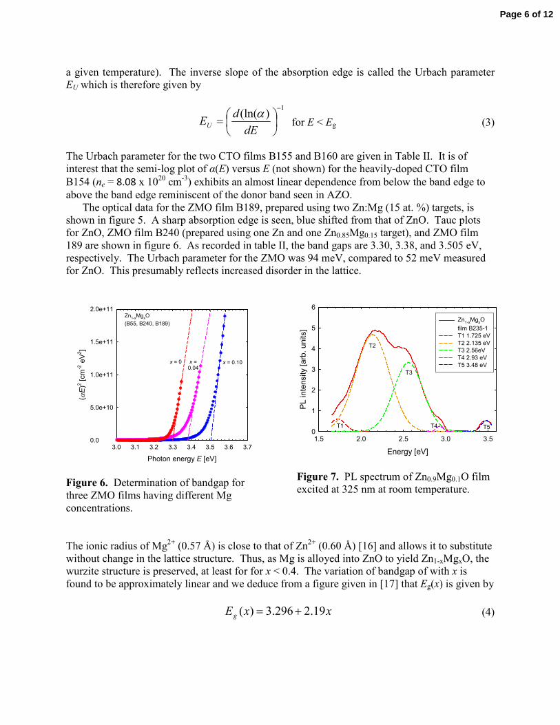
The optical data for the ZMO film B189, prepared using two Zn:Mg (15 at. %) targets, is shown in figure 5. A sharp absorption edge is seen, blue shifted from that of ZnO. Tauc plots for ZnO, ZMO film B240 (prepared using one Zn and one Zn0.85Mg0.15 target), and ZMO film 189 are shown in figure 6. As recorded in table II, the band gaps are 3.30, 3.38, and 3.505 eV, respectively. The Urbach parameter for the ZMO was 94 meV, compared to 52 meV measured for ZnO. This presumably reflects increased disorder in the lattice.
Photon energy E [eV]
3.0 3.1 3.2 3.3 3.4 3.5 3.6 3.7
(αE)2 [cm-2 eV2]
0.0
5.0e+10
1.0e+11
1.5e+11
2.0e+11Zn
1-xMg
xO
(B55, B240, B189)
x = 0 x = 0.04
x = 0.10
Figure 6. Determination of bandgap for three ZMO films having different Mg concentrations.
Energy [eV]
1.5 2.0 2.5 3.0 3.5
PL intensity [arb. units]
0
1
2
3
4
5
6
Zn1-xMg
xO
film B235-1
T1 1.725 eV
T2 2.135 eV
T3 2.56eV
T4 2.93 eV
T5 3.48 eV
T1
T2
T3
T4 T5
Figure 7. PL spectrum of Zn0.9Mg0.1O film excited at 325 nm at room temperature.
The ionic radius of Mg2+ (0.57 Å) is close to that of Zn2+ (0.60 Å) [16] and allows it to substitute without change in the lattice structure. Thus, as Mg is alloyed into ZnO to yield Zn1-xMgxO, the wurzite structure is preserved, at least for for x < 0.4. The variation of bandgap of with x is found to be approximately linear and we deduce from a figure given in [17] that Eg(x) is given by
xxEg 19.2296.3)( += (4)
Page 6 of 12
Based on this equation, the Mg contents in the two ZMO films B240 and B189 are x = 0.04 and 0.10, respectively. For larger values of x phase separation may occur with some MgO (rocksalt structure) occurring. We emphasize that when writing Zn0.9Mg0.1O the x = 0.1 value was deduced from film optical data and not from physical measurement of the Mg concentration.
The ZMO films prepared using two Zn0.85Mg0.15 targets were found to exhibit exceptionally bright photoluminescence. The luminescence of ZMO has previously been described by Shibata et al. [18]. PL measurements conducted at room temperature, with 325 nm excitation, yielded the PL spectrum (uncorrected for system response) shown in figure 7. The spectrum was deconvoluted into 5 Gaussian peaks as shown. T5 represents the near band edge emission. T2 and T3 may represent donor-acceptor pair transitions, while T1 may represent recombination of electrons on oxygen donors with valence band holes [19]. By varying the Mg content, which will shift Ec and some, but not all, other levels relative to Ev, we may hope to better identify the origins of the observed transitions. Temperature stability of CTO films
Many TCO materials are degraded after high temperature annealing or processing [10]. We
found, for example, that ZnO:Al increased in resistivity by 20% after only 15 minutes at 375°C. On the other hand, we found that a CdxSnyO (CTO) film heated for 15 minutes at 400°C with a CdS/glass resting on top decreased in resistivity by 7% and increased in optical transmittance by 1%. These transmittance figures (Tglass+film/Tglass) were obtained using a white LED as a light source and a Si detector. The measurements are shown in table III. Similar results were obtained even at an annealing temperature of 550°C. The study demonstrates that CTO films produced by HCS can withstand the high temperature processing involved in CdTe device fabrication.
Table III. Annealing studies performed on CdxSnyO films.
Run
#
Anneal
status
Thick-
ness t
(nm)
Carrier
conc. ne
(/cm3)
Mobility
µ
(cm2/Vs)
Resistivity
ρ
(Ω cm)
Rsh
(Ω/sq.)
Transm.
(%)
235 before 310 3.78 x 10²⁰ 44.8 3.68 x 10⁻⁴ 11.8 84.7
235 after 306 4.49 x 10²⁰ 40.7 3.42 x 10⁻⁴ 11.2 85.8
Device properties
The superstrate devices being investigated in this program have the general structure:
glass/TCO/window/CdTe/ohmic contact. With ZMO replacing CdS as the window layer, the band diagram of this type 1 (straddling) heterojunction device becomes that shown in figure 8.
Page 7 of 12
Distance
-0.1 0.0 0.1 0.2 0.3
Energy [eV]
-2
-1
0
1
2
n-ZMO p-CdTe
∆Ec
EFp
EFn
Figure 8. Schematic band diagram for the ZMO/CdTe straddling heterojunction interface region showing a ∆Ec < 0 band offset (several features not to scale).
Wavelength [nm]
300 400 500 600 700 800 900
Quantum efficiency
0.0
0.1
0.2
0.3
0.4
0.5
0.6
0.7
0.8
0.9
1.0
glass/FTO/CdS/CdTe
glass/FTO/RF Zn1-xMg
xO/CdTe
glass/FTO/HCS Zn1-xMg
xO/CdTe
glass/FTO/HCS Zn1-xMg
xO/CdTe
Jsc = 25.8 mA cm
-2
Jsc = 20.4 mA cm
-2
Figure 9. External quantum efficiency versus wavelength for cells with CdS, RF ZMO, and HCS ZMO buffer layers.
The ranges of some of the relevant material parameters needed to construct such a diagram are shown in table IV. From Anderson’s rule, the conduction band offset ∆Ec between the absorber and the window layers is given by
abswindow
window
c
abs
cc EEE χχ −=−=∆ (5)
where χ is the electron affinity of the layer in question. By raising the Ec of the Zn1-xMgxO window layer by introducing Mg, the magnitude of ∆Ec can be brought into the favorable range of 0.1 – 0.3 eV (spike rather than cliff offset). The introduction of ZMO into thin-film solar cells was first studied in the context of CIGS [2, 3, 20-22] and later in CdTe [23].
Table IV. Some film parameters pertinent to determination of the band diagram.
Using the Zn0.9Mg0.1O described above in devices fully fabricated at NJIT with the structure glass/FTO/ZMO/CdTe or glass/CTO/ZMO/CdTe has enabled us to almost completely eliminate the blue loss previously resulting from optical absorption in the dead CdS layer. This statement is supported by the dramatic improvement in external quantum efficiency (EQE) for λ < 550 nm exhibited by devices using ZMO as a window layer. This is shown in figure 9. At 400 nm, for example, the EQE can be more than doubled. The short-circuit density implied by integration of the best measured EQE multiplied by the 100 mW cm-2 AM1.5 solar photon flux distribution is 25.8 mA cm-2 for a device with ZMO compared to 20.4 mA cm-2 for a standard device with CdS.
Page 8 of 12
Cadmium sulfide has been used in CdTe solar cells for more than 40 years, and despite the impressive results recently reported by the CSU group [24], it still came as a surprise that we could substitute ZMO for CdS and immediately make working solar cells with high yields. Earlier work in the CIGS area identified seven distinct benefits resulting from the use of a CdS buffer layer deposited by chemical bath deposition [25] and much effort has been expended in trying to develop a satisfactory replacement. There is no consistency in the literature regarding use or definition of the terms window and buffer; here, since the CdS has been eliminated, we prefer to use the term window layer. At a minimum, the ZMO is successful in the roles of HRT (high resistance transparent) layer, wide-gap window layer, control of the ∆Ec
abs-window band
offset, and apparently also as the n+ layer in an n+ p heterojunction. For the glass/FTO/ZMO/CdTe cells we observed that the linear dark J –V curves maintained
a conventional diode shape with low series resistance and high shunt resistance in the dark. Interestingly, however, the curves exhibited an increased turn-on voltage relative to that obtained using CdS, as shown in figure 10. In this paper we define a dark J –V voltage shift Vsh,d (at a fixed current density) as VZMO,d (5 mA cm-2) – VCdS,d (5 mA cm-2). The magnitude of Vsh,d was found to correlate with ZMO thickness, with oxygen flow perhaps also playing a role, and possibly other (non-ZMO related) hidden parameters.
Voltage [V]
-0.4 -0.2 0.0 0.2 0.4 0.6 0.8 1.0 1.2
Current density [mA cm-2]
0
5
10
15
20
FTO/CdS/CdTe
FTO/Zn1-xMg
xO (thick)/CdTe
FTO/Zn1-xMg
xO (thin)/CdTe
voltageshift
Figure 10. Dark J-V characteristics for CdS/CdTe and two ZMO/CdTe solar cells on FTO revealing the substantial voltage shift obtainable with ZMO.
Voltage [V]
0.4 0.5 0.6 0.7 0.8 0.9 1.0 1.1 1.2
Ln(JD mA/cm2)
-6
-4
-2
0
2
4
6
ZMO/CdTe
CdS/CdTe 25 mA/cm
2
A = 3.00A = 1.85
Figure 11. Semi-log dark J-V plot for CdS/CdTe and ZMO/CdTe solar cells.
A significant difference in the semi-log plots of dark J –V was found for devices with CdS
and ZMO window layers, as shown in figure 11. Diode ideality factors of 1.85 and 3.0 were observed for the two types of device.
We may confidently predict that sufficiently large ∆Ec offsets will enter into the transport properties of these heterojunction devices as carriers have to surmount the ∆Ec barrier by thermionic emission. For barriers > 0.4 eV it is easily calculated that thermionic emission cannot support a photocurrent density of 25 mA cm-2 and so reduced collection will occur. We might also expect the dark current to be modulated by a factor
Page 9 of 12
∆−=
kT
Ef cexp (6)
which can account for the observed shift in the dark J –V.
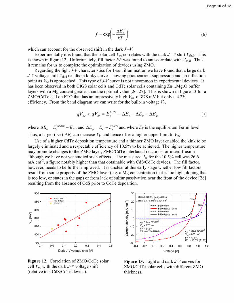
Experimentally it is found that the solar cell Voc correlates with the dark J –V shift Vsh,d. This is shown in figure 12. Unfortunately, fill factor FF was found to anti-correlate with Vsh,d. Thus, it remains for us to complete the optimization of devices using ZMO.
Regarding the light J-V characteristics for 1-sun illumination we have found that a large dark J-V voltage shift Vsh,d results in kinky curves showing photocurrent suppression and an inflection point as Voc is approached. This type of J-V curve is not uncommon in experimental devices. It has been observed in both CIGS solar cells and CdTe solar cells containing Zn1-xMgxO buffer layers with a Mg content greater than the optimal value [26, 27]. This is shown in figure 13 for a ZMO/CdTe cell on FTO that has an impressively high Voc of 878 mV but only a 4.2% efficiency. From the band diagram we can write for the built-in voltage Vbi
pnc
CdTe
gbioc EEEEqVqV ∆−∆−∆−=< [7]
where F
window
cn EEE −=∆ , and CdTe
vFp EEE −=∆ and where EF is the equilibrium Fermi level.
Thus, a larger (-ve) cE∆ can increase Vbi and hence offer a higher upper limit to Voc.
Use of a higher CdTe deposition temperature and a thinner ZMO layer enabled the kink to be largely eliminated and a respectable efficiency of 10.5% to be achieved. The higher temperature may promote changes to the ZMO layer, ZMO/CdTe interfacial reactions, or interdiffusion although we have not yet studied such effects. The measured Jsc for the 10.5% cell was 26.6 mA cm-2, a figure notably higher than that obtainable with CdS/CdTe devices. The fill factor, however, needs to be further improved. It is unclear at this early stage whether low fill factors result from some property of the ZMO layer (e.g. a Mg concentration that is too high, doping that is too low, or states in the gap) or from lack of sulfur passivation near the front of the device [28] resulting from the absence of CdS prior to CdTe deposition.
Dark J-V voltage shift [V]
-0.1 0.0 0.1 0.2 0.3 0.4 0.5
Voc [mV]
780
800
820
840
860
880
900
FTO/ZMO
Plot 1 Regr
FTO/CdS
Figure 12. Correlation of ZMO/CdTe solar cell Voc with the dark J-V voltage shift (relative to a CdS/CdTe device).
Voltage [V]
-0.4 -0.2 0.0 0.2 0.4 0.6 0.8 1.0 1.2
Current density [mA cm-2]
-30
-20
-10
0
10
20
30
B276 dark
B276 light (1 sun)
B260 dark
B260 light (1 sun)
glass/FTO/Zn1-xMg
xO/CdTe
area: 0.179 cm2 / 0.174 cm
2
Jsc = 26.6 mA/cm
2
Voc = 823 mV
FF = 47.8%Eff. = 10.5% (B276)
Jsc = 22.0 mA/cm
2
Voc = 878 mV
FF = 21.6%Eff. = 4.2% (B260)
B276
B260
Figure 13. Light and dark J-V curves for ZMO/CdTe solar cells with different ZMO thickness.
Page 10 of 12
CONCLUSIONS
A custom-built hollow cathode sputtering (HCS) system was used to prepare high quality
CTO and ZMO layers for use in CdTe solar cells. CTO layers with carrier concentrations up to 1.05 x 10²¹ /cm3 or mobilities up to 46.5 cm2/Vs were demonstrated. Carrier concentrations in ZMO could be controlled over the range 1015 – 1019 /cm3. High Voc’s up to 878 mV and Jsc’s up to 26 mA/cm2 obtained in a preliminary round of experiments demonstrate that ZMO provides a means to obtain competitive CdTe solar cells without use of a CdS buffer layer. Various temperature-dependent studies are expected to shed light on the window-absorber band offset and the activation energy of the dominant recombination path. The flexibility of HCS to produce almost any type of metal oxide offers a route for comprehensive optimization of the entire front side (TCO/window layer) of thin film CdTe solar cells.
ACKNOWLEDGMENTS
The research was supported by a two-year Research Agreement executed between NJII and
CTIEC.
REFERENCES
1. X. Wu, J.C. Keane, R.G. Dhere, C. DeHart, D.S. Albin, A. Duda, T.A. Gessert, S. Asher,
D.H. Levi, and P. Sheldon, Proc. 17th
Eur. Photovolt. Sol. Energy Conf. (James & James Ltd., London, 2001) pp. 995-1000.
2. T. Minemoto, Y. Hashimoto, W. Shams-Kolahi, T. Satoh, T. Negami, H. Takakura, and Y. Hamakawa, Sol. Energy Mater. Sol. Cells 75, 121-126 (2003).
3. A. Yamada, K. Matsubara, K. Sakurai, S. Ishizuka, H. Tampo, P.J. Fons, K. Iwata, and S. Niki, Appl. Phys. Lett. 85, 5607-5609 (2004).
4. J.N. Duenow, J.M. Burst, D.S. Albin, M.O. Reese, S.A. Jensen, S.W. Johnston, D. Kuciauskas, S.K. Swain, T Ablekim, K.G. Lynn, A.L. Fahrenbruch, and W.K. Metzger, IEEE J. Photovolt. 6, 1641-1644 (2016).
5. D.E. Swanson, J.R. Sites, and W.S. Sampath, Sol. Energy Mater. Sol. Cells 159, 389-394 (2017).
6. M. Gloeckler, I. Sankin, and Z. Zhao, IEEE J. Photovolt. 3, 1389-1393 (2013). 7. J.M. Burst, J.N. Duenow, D.S. Albin, E. Colegrove, M.O. Reese, J.A. Aguiar, C-S. Jiang,
M.K. Patel, M.M. Al-Jassim, D. Kuciauskas, and S. Swain, Nat. Energy 1, 16015, (2016). 8. Y. Zhao, M. Boccard, S. Liu, J. Becker, X-H. Zhao, C.M. Campbell, E. Suarez, M.B.
Lassise, Z. Holman, and Y-H. Zhang, Nat. Energy 1, 16067 (2016). 9. A.E. Delahoy, S. Falk, P. Patra, R. Korotkov, B. Siepchen, S. Peng, and K.K. Chin, 43
rd
IEEE Photovolt. Specialist Conf. 1443-1448 (2016). 10. A.E. Delahoy and S. Guo, Transparent Conductive Oxides for Photovoltaics, Chapter 17
in Handbook of Photovoltaic Science and Engineering, 2nd Edition, Edited by A. Luque and S. Hegedus (Wiley, Chichester, 2011) pp. 716-796.
Page 11 of 12
11. V. Krishnakumar, B. Späth, C. Drost, C. Kraft, B. Siepchen, A. Delahoy, X. Tan, K. Chin, S. Peng, D. Hirsch, O. Zywitzki, T. Modes, and H. Morgner, Thin Solid Films (2016).
12. R. Mamazza, D.L. Morel, and C.S. Ferekides, Thin Solid Films 484, 26-33 (2005). 13. T. Meng, B. McCandless, W. Buchanan, E. Kimberly, and R. Birkmire, J. Alloy
Compd. 556, 39-44 (2013). 14. E. Leja, T. Stapiński, and K. Marszałek, Thin Solid Films 125, 119-122 (1985). 15. S.B. Zhang and S.H. Wei, Appl. Phys. Lett. 80, 1376-1378 (2002). 16. R.D. Shannon, Acta Cryst. A32, 751-767 (1976). 17. M. Lorenz, E.M. Kaidashev, H. Von Wenckstern, V. Riede, C. Bundesmann, D.
Spemann, G. Benndorf, H. Hochmuth, A. Rahm, H.C. Semmelhack, and M. Grundmann, Solid-St. Electron. 47, 2205-2209 (2003).
18. H. Shibata, H. Tampo, K. Matsubara, A. Yamada, K. Sakurai, S. Ishizuka, S. Niki, and M. Sakai, Appl. Phys. Lett. 90, 124104 (2007).
19. M. Trunk, V. Venkatachalapathy, A. Galeckas, and A.Y. Kuznetsov, Appl. Phys. Lett. 97, 211901 (2010).
20. J.V. Li, X. Li, Y. Yan, C-S. Jiang, W.K. Metzger, I.L. Repins, M.A. Contreras, and D.H. Levi, J. Vac. Sci. Technol. B 27, 2384-2389 (2009).
21. F. Erfurth, A. Grimm, J. Palm, T.P. Niesen, F. Reinert, L. Weinhardt, and E. Umbach, Appl. Phys. Lett. 98, 142107 (2011).
22. C.S. Lee, S. Kim, Y.M. Shin, B.G. Park, B.T. Ahn, and H. Kwon, RSC Adv. 4, 36784-36790 (2014).
23. T. Song, A. Kanevce, and J.R. Sites, J. Appl. Phys. 119, 233104 (2016). 24. J. Sites, A. Munshi, J. Kephart, D. Swanson, and W.S. Sampath, 43
rd IEEE Photovolt.
Specialist Conf. 3632-3635 (2016). 25. A.E. Delahoy, M. Akhtar, J. Cambridge, L. Chen, R. Govindarajan, S. Guo, and M.J.
Romero, 29th
IEEE Photovolt. Specialist Conf. 640-643 (2002). 26. T. Törndahl, C. Platzer-Björkman, J. Kessler, and M. Edoff, Prog. Photovolt: Res.
Appl. 15, 225-235 (2007). 27. J.M. Kephart, J.W. McCamy, Z. Ma, A. Ganjoo, F.M. Alamgir, and W.S. Sampath, Sol.
Energy Mater. Sol. Cells 157, 266-275 (2016). 28. A.E. Delahoy, Z. Cheng, and K.K. Chin, 39