203


CALIBRATION TECHNIQUES IN NYQUIST A /D CONVERTERS

THE INTERNATIONAL SERIES IN ENGINEERING AND COMPUTER SCIENCE
ANALOG CIRCUITS AND SIGNAL PROCESSING Consulting Editor: Mohammed Ismail. Ohio State University
Related Titles: WIDE-BANDWIDTH HIGH-DYNAMIC RANGE D/A CONVERTERS
Doris,Konstantinos, van Roermund, Arthur, Leenaerts, Domine Vol. 871 ISBN: 0-387-30415-0
METHODOLOGY FOR THE DIGITAL CALIBRATION OF ANALOG CIRCUITS AND SYSTEMS: WITH CASE STUDIES
Pastre, Marc, Kayal, Maher Vol. 870, ISBN: 1-4020-4252-3
HIGH-SPEED PHOTODIODES IN STANDARD CMOS TECHNOLOGY Radovanovic, Sasa, Annema, Anne-Johan, Nauta, Bram Vol. 869, ISBN: 0-387-28591-1
LOW-POWER LOW-VOLTAGE SIGMA-DELTA MODULATORS IN NANOMETER CMOS Yao, Libin, Steyaert, Michiel, Sansen, Willy Vol. 868, ISBN: 1-4020-4139-X
DESIGN OF VERY HIGH-FREQUENCY MULTIRATE SWITCHED-CAPACITOR CIRCUITS U, Seng Pan, Martins, Rui Paulo, Epifänio da Franca, José Vol. 867, ISBN: 0-387-26121-4
DYNAMIC CHARACTERISATION OF ANALOGUE-TO-DIGITAL CONVERTERS Dallet, Dominique; Machado da Silva, José(Eds.) Vol. 860, ISBN: 0-387-25902-3
ANALOG DESIGN ESSENTIALS Sansen, Willy Vol. 859, ISBN: 0-387-25746-2
DESIGN OF WIRELESS AUTONOMOUS DATALOGGER IC’S Claes and Sansen Vol. 854, ISBN: 1-4020-3208-0
MATCHING PROPERTIES OF DEEP SUB-MICRON MOS TRANSISTORS Croon, Sansen, Maes Vol. 851, ISBN: 0-387-24314-3
LNA-ESD CO-DESIGN FOR FULLY INTEGRATED CMOS WIRELESS RECEIVERS Leroux and steyaert Vol. 843, ISBN: 1-4020-3190-4
SYSTEMATIC MODELING AND ANALYSIS OF TELECOM FRONTENDS AND THEIR BUILDING BLOCKS Vanassche, Gielen, Sansen Vol. 842, ISBN: 1-4020-3173-4
LOW-POWER DEEP SUB-MICRON CMOS LOGIC SUB-THRESHOLD CURRENT REDUCTION Van der Meer, van Staveren, van Roermund Vol. 841, ISBN: 1-4020-2848-2
WIDEBAND LOW NOISE AMPLIFIERS EXPLOITING THERMAL NOISE CANCELLATION Bruccoleri, Klumperink, Nauta Vol. 840, ISBN: 1-4020-3187-4
CMOS PLL SYSTHESIZERS: ANALYSIS AND DESIGN Shu, Keliu, Sánchez-Sinencio, Edgar Vol. 783, ISBN: 0-387-23668-6
SYSTEMATIC DESIGN OF SIGMA-DELTA ANALOG-TO-DIGITAL CONVERTERS Bajdechi and Huijsing Vol. 768, ISBN: 1-4020-7945-1
OPERATIONAL AMPLIFIER SPEED AND ACCURACY IMPROVEMENT Ivanov and Filanovsky Vol. 763, ISBN: 1-4020-7772-6
STATIC AND DYNAMIC PERFORMANCE LIMITATIONS FOR HIGH SPEED D/A CONVERTERS Van den Bosch, Steyaert and Sansen Vol. 761, ISBN: 1-4020-7761-0
DESIGN AND ANALYSIS OF HIGH EFFICIENCY LINE DRIVERS FOR Xdsl Piessens and Steyaert Vol. 759, ISBN: 1-4020-7727-0
LOW POWER ANALOG CMOS FOR CARDIAC PACEMAKERS Silveira and Flandre Vol. 758, ISBN: 1-4020-7719-X
MIXED-SIGNAL LAYOUT GENERATION CONCEPTS Lin, van Roermund, Leenaerts Vol. 751, ISBN: 1-4020-7598-7

and
Philips Research, Eindhoven, The Netherlands
University of Twente, Enschede, The Netherlands
Hendrik van der Ploeg
By
Bram Nauta
CALIBRATION TECHNIQUES IN NYQUIST
A/D CONVERTERS

A C.I.P. Catalogue record for this book is available from the Library of Congress.
Published by Springer,P.O. Box 17, 3300 AA Dordrecht, The Netherlands.
Printed on acid-free paper
All Rights Reserved
No part of this work may be reproduced, stored in a retrieval system, or transmittedin any form or by any means, electronic, mechanical, photocopying, microfilming, recording
or otherwise, without written permission from the Publisher, with the exceptionof any material supplied specifically for the purpose of being entered
and executed on a computer system, for exclusive use by the purchaser of the work.
Printed in the Netherlands
© 2006 Springer
www.springer.com
ISBN-10 1-4020-4634-0 (HB)ISBN-13 978-1-4020-4634-6 (HB)ISBN-10 1-4020-4635-9 (e-book)ISBN-13 978-1-4020-4635-9 (e-book)

Aan Ria en mijn ouders

Table of contents
List of abbreviations
List of symbols
Preface
1 Introduction 11.1 A/D conversion systems . . . . . . . . . . . . . . . . . . . . . . 11.2 Motivation and objectives . . . . . . . . . . . . . . . . . . . . . . 51.3 Layout of the book . . . . . . . . . . . . . . . . . . . . . . . . . 5
2 Accuracy, speed and power relation 72.1 Introduction . . . . . . . . . . . . . . . . . . . . . . . . . . . . . 72.2 IC-technology accuracy limitations . . . . . . . . . . . . . . . . . 8
2.2.1 Process mismatch . . . . . . . . . . . . . . . . . . . . . . 82.2.22.2.3 Matching versus noise requirements . . . . . . . . . . . . 11
2.3 Speed and power . . . . . . . . . . . . . . . . . . . . . . . . . . 112.4 Maximum speed . . . . . . . . . . . . . . . . . . . . . . . . . . . 132.5 . . . . . . . . . . . . . . . . . . . . . 152.6 Conclusions . . . . . . . . . . . . . . . . . . . . . . . . . . . . . 18
3 A/D converter architecture comparison 213.1 Introduction . . . . . . . . . . . . . . . . . . . . . . . . . . . . . 213.2 Flash . . . . . . . . . . . . . . . . . . . . . . . . . . . . . . . . . 22
3.2.1 Full flash . . . . . . . . . . . . . . . . . . . . . . . . . . 233.2.2 Interpolation . . . . . . . . . . . . . . . . . . . . . . . . 263.2.3 Averaging . . . . . . . . . . . . . . . . . . . . . . . . . . 29
3.3 Folding and interpolation . . . . . . . . . . . . . . . . . . . . . . 333.4 Two-step . . . . . . . . . . . . . . . . . . . . . . . . . . . . . . . 38
Thermal noise . . . . . . . . . . . . . . . . . . . . . . . 10
CMOS technology trends
xi
xiii
xvii

Table of contents
3.5 Pipe-line . . . . . . . . . . . . . . . . . . . . . . . . . . . . . . . 463.6 Successive approximation . . . . . . . . . . . . . . . . . . . . . . 543.7 Theoretical power consumption comparison . . . . . . . . . . . . 56
3.7.1 Figure-of-Merit (FoM) . . . . . . . . . . . . . . . . . . . 573.7.2 Architecture comparison as a function of the resolution . . 573.7.3 Architecture comparison as a function of the sampling speed 65
3.8 Conclusions . . . . . . . . . . . . . . . . . . . . . . . . . . . . . 66
4 Enhancement techniques for two-step A/D converters 674.1 Introduction . . . . . . . . . . . . . . . . . . . . . . . . . . . . . 674.2 Error sources in a two-step architecture . . . . . . . . . . . . . . 674.3 Residue gain in two-step A/D converters . . . . . . . . . . . . . . 69
4.3.1 Single-residue signal processing . . . . . . . . . . . . . . 694.3.2 Dual-residue signal processing . . . . . . . . . . . . . . . 714.3.3 Conclusions . . . . . . . . . . . . . . . . . . . . . . . . . 75
4.4 Offset calibration . . . . . . . . . . . . . . . . . . . . . . . . . . 754.4.1 Introduction . . . . . . . . . . . . . . . . . . . . . . . . . 754.4.2 Calibration overview . . . . . . . . . . . . . . . . . . . . 754.4.3 Conclusions . . . . . . . . . . . . . . . . . . . . . . . . . 82
4.5 Mixed-signal chopping and calibration . . . . . . . . . . . . . . . 834.5.1 Residue amplifier offset chopping . . . . . . . . . . . . . 834.5.2 Offset extraction from digital output . . . . . . . . . . . . 844.5.3 Pseudo random chopping . . . . . . . . . . . . . . . . . . 884.5.4 Offset extraction and analog compensation . . . . . . . . 914.5.5 Offset extraction in a dual-residue two-step converter . . . 934.5.6 Conclusions . . . . . . . . . . . . . . . . . . . . . . . . . 102
5 A 10-bit two-step ADC with analog online calibration 1035.1 Introduction . . . . . . . . . . . . . . . . . . . . . . . . . . . . . 1035.2
5.2.1 Coarse quantizer accuracy . . . . . . . . . . . . . . . . . 1065.2.2 D/A converter and subtractor accuracy . . . . . . . . . . . 1075.2.3 Coarse and fine A/D converter references . . . . . . . . . 1085.2.4 Amplifier gain and offset accuracy . . . . . . . . . . . . . 109
5.3 Circuit design . . . . . . . . . . . . . . . . . . . . . . . . . . . . 1105.3.1 Track-and-hold circuit . . . . . . . . . . . . . . . . . . . 1115.3.2 Coarse A/D, D/A converter and subtractor . . . . . . . . . 1115.3.3 Coarse ladder requirements . . . . . . . . . . . . . . . . . 1125.3.4 Offset compensated residue amplifier . . . . . . . . . . . 1135.3.5 Fine A/D converter . . . . . . . . . . . . . . . . . . . . . 1145.3.6 Timing . . . . . . . . . . . . . . . . . . . . . . . . . . . 116
viii
Two-Step architecture . . . . . . . . . . . . . . . . . . . . . . . 105

Table of contents
5.4 Experimental results . . . . . . . . . . . . . . . . . . . . . . . . 1175.5 Discussion . . . . . . . . . . . . . . . . . . . . . . . . . . . . . . 1215.6 Conclusions . . . . . . . . . . . . . . . . . . . . . . . . . . . . . 122
6 A 12-bit two-step ADC with mixed-signal chopping and calibration 1236.1 Introduction . . . . . . . . . . . . . . . . . . . . . . . . . . . . . 1236.2 Two-step architecture . . . . . . . . . . . . . . . . . . . . . . . . 126
6.2.1 Interleaved sample-and-hold . . . . . . . . . . . . . . . . 1276.2.2 Coarse A/D converter . . . . . . . . . . . . . . . . . . . . 1286.2.3 Switching and residue signal generation . . . . . . . . . . 1296.2.4 Residue amplifiers . . . . . . . . . . . . . . . . . . . . . 132
6.3 Mixed-signal chopping and calibration . . . . . . . . . . . . . . . 1336.3.1 Residue amplifier offset . . . . . . . . . . . . . . . . . . 1346.3.2 Chopping . . . . . . . . . . . . . . . . . . . . . . . . . . 1346.3.3 Digital extraction . . . . . . . . . . . . . . . . . . . . . . 135
6.4 Circuit design . . . . . . . . . . . . . . . . . . . . . . . . . . . . 1366.4.1 Interleaved sample-and-hold . . . . . . . . . . . . . . . . 1366.4.2 Coarse A/D converter . . . . . . . . . . . . . . . . . . . . 1376.4.3 Residue amplifier with offset compensating current D/A
converter . . . . . . . . . . . . . . . . . . . . . . . . . . 1386.4.4 Folding-and-interpolating fine A/D converter . . . . . . . 139
6.5 Experimental results . . . . . . . . . . . . . . . . . . . . . . . . 1416.6 Discussion . . . . . . . . . . . . . . . . . . . . . . . . . . . . . . 1456.7 Conclusions . . . . . . . . . . . . . . . . . . . . . . . . . . . . . 146
7 A low-power 16-bit three-step ADC for imaging applications 1497.1 Introduction . . . . . . . . . . . . . . . . . . . . . . . . . . . . . 1497.2 Three-step architecture . . . . . . . . . . . . . . . . . . . . . . . 151
7.2.1 Sample-and-hold . . . . . . . . . . . . . . . . . . . . . . 1537.2.2 Resolution distribution . . . . . . . . . . . . . . . . . . . 1547.2.3 Switching . . . . . . . . . . . . . . . . . . . . . . . . . . 154
7.3 Noise considerations . . . . . . . . . . . . . . . . . . . . . . . . 1567.4 Mixed-signal chopping and calibration . . . . . . . . . . . . . . . 158
7.4.1 Mid and fine residue amplifier stage calibration . . . . . . 1587.4.2 Quick calibration . . . . . . . . . . . . . . . . . . . . . . 160
7.5 Supply voltages . . . . . . . . . . . . . . . . . . . . . . . . . . . 1617.6 Experimental results . . . . . . . . . . . . . . . . . . . . . . . . 1627.7 Discussion . . . . . . . . . . . . . . . . . . . . . . . . . . . . . . 1677.8 Conclusions . . . . . . . . . . . . . . . . . . . . . . . . . . . . . 168
ix

Table of contents
8 Conclusions 169
A Static and dynamic accuracy requirements 173A.1 Static error requirments . . . . . . . . . . . . . . . . . . . . . . . 173A.2 Dynamic error requirements . . . . . . . . . . . . . . . . . . . . 175
References 177
Index 189
x

List of abbreviations
A/D analog-to-digitalADC analog-to-digital converterAMP amplifierATV analog televisionCCD charge-coupled deviceCDS correlated double samplingCMOS complementary metal oxide semiconductorCVBS composite video baseband signalD/A digital-to-analogDAC digital-to-analog converterDC direct currentDNL differential non-linearityDSP digital signal processorDTV digital televisionEDGE enhanced data rates for GSM evolutionENOB effective-number-of-bitsEPROM electrically-programmable read-only memoryERBW effective resolution bandwidthGSM global system for mobile communicationIC integrated circuitINL integral non-linearityINT integratorLSB least-significant-bitMSB most-significant-bitMSCC mixed-signal chopping and calibrationOPAMP operational amplifierOR over-rangePCB printed circuit boardPROM programmable read-only memory
xi

List of abbreviations
RAM random-access memoryRF radio frequencyROM read-only memorySAR successive approximationSFDR spurious free dynamic rangeS/H sample-and-holdSHA sample-and-hold amplifierSINAD signal-to-noise and distortionSiP system-in-packageSNR signal-to-noise ratioSoC system-on-a-chipSUB subrangeT/H track-and-holdTHA track-and-hold amplifierTHD total harmonic distortionUR under-rangeVGA variable gain amplifierXOR exclusive orYUV luminance and chrominance signals
xii

List of symbols
a ratio between fin, fs and fc -A gain factor -AC capacitor mismatch process parameter
√C
Afa folding amplifier gain -AVT
threshold mismatch process parameter mVµmAβ current factor mismatch process parameter %µmC symbol for capacitance FCgs gate-source capacitance FCintr minimum required capacitance FCLOAD load capacitance FCmatching capacitance resulting from matching requirement FCminimum minimum required capacitance FCnoise capacitance resulting from noise requirement FCox oxide capacitance per unit area F/m2
Cp parasitic capacitance FCx F
DRpp peak-to-peak signal to rms noise dBENOB, DC effective-number-of-bits at DC -f−3dB 3 dB frequency HzFf folding factor -Fint interpolation factor -FoM figure-of-merit pJFoMVpp figure-of-merit normalized to 1 Vpp V2pJfc chop signal frequency HzfENOB,DC−0.5 frequency with 0.5 ENOB loss in ENOB w.r.t.
ENOB, DCHz
fin input signal frequency Hzfs sample frequency Hz
requirementscapacitance determined by noise or matching
−
xiii
□
□
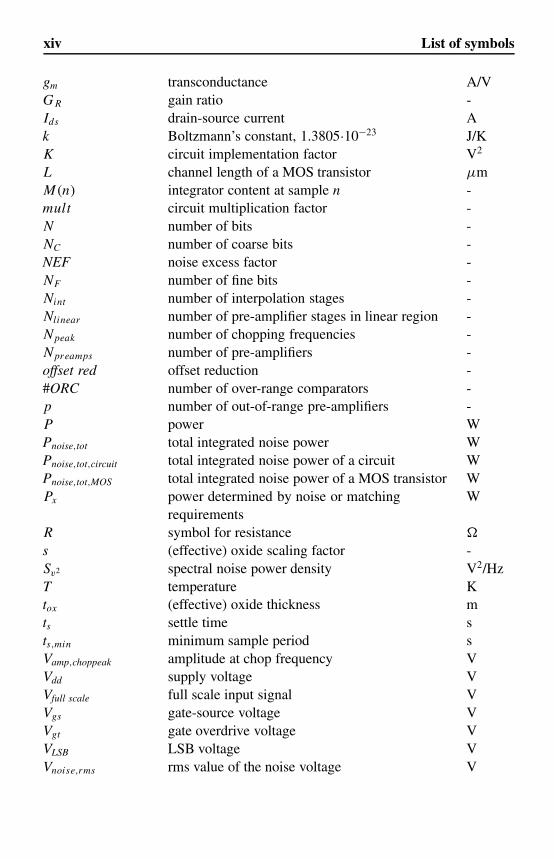
List of symbols
gm transconductance A/VGR gain ratio -Ids drain-source current Ak Boltzmann’s constant, 1.3805·10−23 J/KK circuit implementation factor V2
L channel length of a MOS transistor µmM(n) integrator content at sample n -mult circuit multiplication factor -N number of bits -NC number of coarse bits -NEF noise excess factor -NF number of fine bits -Nint number of interpolation stages -Nlinear number of pre-amplifier stages in linear region -Npeak number of chopping frequencies -Npreamps number of pre-amplifiers -offset red offset reduction -#ORC number of over-range comparators -p number of out-of-range pre-amplifiers -P power WPnoise,tot total integrated noise power WPnoise,tot,circuit total integrated noise power of a circuit WPnoise,tot,MOS total integrated noise power of a MOS transistor WPx W
R symbol for resistance �
s (effective) oxide scaling factor -Sv2 spectral noise power density V2/HzT temperature Ktox (effective) oxide thickness mts settle time sts,min minimum sample period sVamp,choppeak amplitude at chop frequency VVdd supply voltage VVfull scale full scale input signal VVgs gate-source voltage VVgt gate overdrive voltage VVLSB LSB voltage VVnoise,rms rms value of the noise voltage V
requirementspower determined by noise or matching
xiv

List of symbols
Voffset offset voltage VVpp peak-to-peak voltage VVrms rms value of the voltage VVshift,n nth reference voltage VVsignal,rms rms value of the signal voltage VVT threshold voltage VW channel width of a MOS transistor µmx ratio between coarse comparator and residue
amplifier offset-
xNF normalizing factor for equal data rate -β current factor µA/V2
�C error in the capacitance Fε settling error -εcoarse quantization coarse quantization error -εfine quantization fine quantization error -εfine range fine range error -εgain gain error -εoffset offset error -εreference reference error -εsubtraction subtraction error -γ white noise factor -µn,p mobility of electrons, holes cm2/Vsπ pi, 3.141593 -σ standard deviation -σC spread of the capacitance FσVoffset spread of the offset voltage Vτ time constant sτmin minimum achievable time constant sτunit time constant of one buffer unit s
xv
□

Preface
The advances in Integrated Circuits brought us advanced electronic systems avail-able for large groups of people. By putting more and more functionality on an in-tegrated circuit (IC) these systems could become cheap in mass production. Many
Today, most electronic systems process signals in digital format. This way low-cost accurate circuits with a very high density can be made. The signals in the
It is beneficial to integrate these A/D and D/Aconverters in the same IC as the digital functions for cost and size reasons. Sincethe digital ICs are generally implemented in CMOS technology, this requires A/Dand D/A converters in CMOS as well, which poses quite some challenges in thedesign since CMOS technology is optimized for digital circuits.
Analog-to-digital converters can roughly be split in two families. The first fam-ily is the one of the high accuracy and low speed converters, often referred to asoversampled converters, typically used for audio and low MHz range. In theseconverters the speed of the technology is exploited to relax the accuracy demandsof the analog circuits. The second family is the one of the high speed, mediumaccuracy converters, also referred to as Nyquist converters. Here oversamplingcannot be used and the accuracy has to come from the analog circuits itself. Ac-curacy is generally achieved by relying on matching of equally designed on-chipcomponents, which works better for larger-size components on a chip. However iflarge components have to work at high speed, this requires high power dissipation.So these converters generally have a trade-off in power, speed and accuracy.
This book deals with Nyquist-type converters. The basic idea exploited here is touse the available digital processing power of the CMOS technology to calibratecritical analog parts of the A/D converter. This way the analog accuracy demandsof the components can be relaxed and smaller sized-components can be used, res-ulting in a reduction in power consumption. This book starts with an introductionin the field, exploring the power, accuracy and speed space. The conclusion is thattwo-step converters form a good base for investigating the calibration techniques.
researchers work on the advances in integration of complex systems.
to-analog converters are required.real world however are all analog, and therefore analog-to-digital and digital-
xvii

Preface
In the remaining chapters several calibration algorithms are described, and severalIC realizations of calibrated two-step converters are presented.
The book was originally the PhD thesis of Hendrik van der Ploeg who wrote itafter 9 years of experience in A/D converter design at Philips Research laborat-ories. I really enjoyed working with Hendrik to prepare his thesis and now I feelvery happy that it has been published as a book. I believe this book is really worthreading for a broad group of scientists and engineers.
Bram Nauta,Professor,University of Twente,The Netherlands
Enschede, January 2006
xviii

Chapter 1
Introduction
1.1 A/D conversion systems
In modern systems, most of the signal processing is performed in the digital do-main. Digital circuits have a lower sensitivity to noise and are less susceptibleto fluctuations in supply and process variations. Unlike with analog circuits, sig-nal processing in the digital domain offers greater programmability, error correc-tion and storage possibilities. Since the world around us is analog and humans
They are found inmany systems that require digital signal processing. This book focuses on A/Dconverters. A/D converters can be classified into two groups. There are A/D con-verters with a high accuracy and a low sample rate and A/D converters with a lowaccuracy and a high sample rate. This is illustrated in figure 1.1.
The first group includes sigma-delta converters for audio, signal transmissionand instrumentation systems, while the second group includes video, camera andwide-band signal transmission systems. In order to increase the accuracy or thespeed specifications of the A/D converters in both groups more power is required.The A/D converters from the second group of converters are dealt with in thisbook. They are found in products like television sets, security cameras, medicalimaging devices, instrumentation, etc. The sampling speed required for these ap-plications is generally in excess of 25 MSample/s and the resolution is 10 bits ormore. A few examples of these applications are shown in figure 1.2.
The position of the A/D converter in such systems is shown in figure 1.3. In thisfigure, the signal is conditioned in the analog domain before it is applied to theA/D converter.
1
to-analog (D/A) converters represent important building blocks.perceive information in the analog form, analog-to-digital (A/D) and digital-

2
sample rate [MSps]
resolution [bits]
morepower
lesspower
this work
high resolution,low frequency
low resolution,high frequency
Figure 1.1: High accuracy, low speed A/D converters and low accuracy,high speed A/D converters and the position of this work
Figure 1.2: Systems with A/D converters with sampling speeds in excessof 25 MSample/s and a resolution of 10 bits or more
log world and the digital signal processing and digital memory. For example, theA/D converter converts the down-converted radio frequency (RF) antenna signalto the digital domain. In the case of figure 1.3, the filtering and channel selectionis performed in the analog domain. Another example is an analog video signalwith an aspect ratio of 4:3, which is converted to the digital domain. In the di-gital domain a field memory and additional processing is used to resize the videosignal to an aspect ratio of 16:9. A D/A converter converts this signal back to theanalog domain to be applied to a display [1]. Similar signal processing is required
As shown in figure 1.3, the A/D converters form the connection between the ana-
Introduction

3
MobileCable
ATV/DTV
Communicationpipe
AD
C/D
AC
Sensorpipe
AD
C Storagepipe
AD
C/D
AC
Outputprocessing
DA
C
DigitalProcessing(hardware/software)
Powermanagement
ImageUltrasound
X-ray
OpticalHarddrive
DisplaySound
communication
Power
Figure 1.3: The position of the A/D converter in the system, with signalconditioning in the analog domain
to convert a video signal with a 50 Hz frame rate to a video signal with a 100 Hzframe rate.
The performance level should be such that the system is not affected by the imper-fections of the data converter. Its design is therefore extremely important. Becauseof the trend towards decreasing feature sizes on silicon, it is becoming cheaper toshift analog functions, such as amplifying, filtering and mixing, into the digitaldomain. This involves shifting the A/D converter towards the input of the system;an extreme example of this is shown in figure 1.4.
MobileCable
ATV/DTV
Communicationpipe
AD
C/D
AC
Sensorpipe
AD
C Storagepipe
AD
C/D
AC
Outputprocessing
DA
C
DigitalProcessing(hardware/software)
Powermanagement
ImageUltrasound
X-ray
OpticalHarddrive
DisplaySound
communication
Power
Figure 1.4: The A/D converter shifted towards the input of the system
In order to shift the A/D converter towards the input of such systems, A/D convert-ers are required with a greater dynamic range and higher sampling speeds becausethere is less analog signal conditioning. This makes even higher demands on theA/D converter and potentially increases the power consumption. The calibrationtechniques investigated in this book enables to increase the accuracy without in-creasing the power consumption of the A/D converter.
1.1 A/D conversion systems

4
If the specifications are known from the application, the challenges in the design ofA/D converters arise from the technology used. The application generally determ-ines the integrated circuit (IC) technology, which is mainly a cost-driven choice.Due to the high level of integration of systems on a chip, the digital functional-ity and therefore the area occupied by digital circuitry becomes dominant. Thismeans a technology has to be chosen that is optimized for digital circuitry. In thiscase the technology is optimized for high-density digital circuits, which allows theuse of small feature sizes that achieve a high packing density. The parameters ofthis technology are typically optimized for the digital circuitry and are thereforeless suitable for high-performance analog circuits. On the other hand, there aretechnologies that are better suited for the design of dedicated high-performanceanalog circuits. Although the stand-alone analog circuits can achieve a high per-formance, these components have to be integrated into the overall system at ahigher, system-in- package (SiP) level. This is in contradiction with the increas-ingly higher level of integration of systems-on-a-chip (SoC). However, the useof multi-die packages as shown in figure 1.5 also offers advantages because thedigital circuitry can be designed on a digital chip, in a dedicated digital comple-mentary metal oxide semiconductor (CMOS) technology, whilst the analog cir-cuits are designed in a dedicated analog technology. This allows fast scaling ofthe digital part whilst the analog performance with the analog chip is maintainedand digital cross-talk is prevented.
Figure 1.5: System-in-package (from [2]) with analog TV processor anda digital signal processor
Introduction

5
A/D converter calibration techniques are applicable for any technology, howeverthis book focuses on the design of A/D converters for highly integrated systems.The focus is, therefore, on designing A/D converters in CMOS.
1.2 Motivation and objectives
The main focus of this book is on improving the supply power efficiency of A/Dconverters capable of handling input signal frequencies up to the Nyquist fre-quency by using calibration. The boundary condition is to use standard CMOStechnology without additional options. This allows us to use the A/D converterin a system-on-a-chip with a high level of integration. This book is split up intothree main subjects:
• General analysis of the relation between the specified accuracy and speedand the resulting power for A/D converters.
•able power efficiency.
• Investigation of enhancement techniques instrumental in increasing the levelof accuracy whilst maintaining the power consumption of A/D converters.
The results from these investigations are used in the circuit design and realizationof three A/D converters.
1.3 Layout of the book
In chapter 2 the relation between the required accuracy and speed and the powerconsumption in the design of A/D converters is explained.
be derived. The
For a given accuracy, the total minimum required capacitance of an A/D converteris a strong function of the architecture used. Chapter 3 describes the A/D con-verter architectures which are applicable for the scope of this book. The totalminimum required capacitance is derived for each architecture and this result isused to compare the power consumption of these architectures. A benchmark hasbeen carried out on recently published A/D converters and this is compared to the
Comparison of the various A/D converter architectures with respect to achiev-
generations.consumption. This relation is also investigated over different CMOS technologycalculated capacitance combined with the speed is a measure of the power
The minimum re-quired capacitance, whether determined by matching or noise requirements, will
This capacitance is charged and discharged at a certain speed.
Motivation and objectives1.2

6
theoretical derivation. It is on the basis of this comparison that the two-step A/Dconverter architecture has been selected for further investigation.
In subranging A/D converters, matching of the ranges of the different quantizationstages is very important. Chapter 4 presents dual-residue signal processing [3] inorder to relax this requirement. The next part of chapter 4 deals with calibrationtechniques for reducing the matching requirements and the resulting minimumrequired capacitances. Different calibration techniques are discussed and the the-ory of a developed mixed-signal chopping and calibration (MSCC) algorithm ispresented.
The design and the measurement results of a 10-bit two-step A/D converter arepresented in chapter 5. In this design the dual-residue signal processing togetherwith an analog offset compensation technique is demonstrated. The mixed-signalchopping and calibration algorithm is demonstrated in chapter 7 by means of a12-bit two-step A/D converter. Chapter 7 shows the extension of the two-stepto a 16-bit three-step converter in order to reduce the power consumption of thequantization stages. This design uses two independent mixed-signal chopping andcalibration blocks.
In chapter 8 the main conclusions are summarized and recommendations for fur-ther research are presented.
Introduction

Chapter 2
2.1 Introduction
An A/D converter consists of several building blocks. Each of these buildingblocks has accuracy and speed requirements which are A/D converter architecturedependent. This chapter derives the relation between the accuracy, the speed andthe resulting power consumption. This makes it possible to make a comparisonbetween various A/D converter architectures based on the required accuracy andspeed of the different building blocks.
The static (DC) accuracy of such building blocks is determined by the matching ofcomponents, which is technology dependent. The noise generated in a circuit setsa limit on the achievable
’
dynamic’ accuracy. In analog circuit design there aretwo main sources of noise: noise that arises as a result of a non-ideal environment(such as supply or ground noise) and noise from passive and active electronicdevices. These sources of noise reduce the quality of the analog output signal ofthe circuit. Here only the electronic device noise is considered. In general, bothmismatch and noise determine the quality of the conversion of a signal from theanalog domain to the digital domain, assuming accurate timing. Section 2.2 showsthat in order to guarantee a certain degree of accuracy in a given technology, the re-quired conversion quality results in minimum device sizes and therefore minimumrequired capacitances. This minimum required capacitance together with the con-version speed is a measure for the minimum required power consumption, whichis described in section 2.3. The minimum required capacitance is connected to abuffer which has its own parasitic capacitance. When this parasitic capacitance islarger than the load capacitance, the speed is limited by this parasitic capacitance.
power relation
7
Accuracy, speed and

8
The maximum achievable speed is discussed in section 2.4. Since the parametersthat determine the accuracy and the speed are technology dependent, some trendsin CMOS technologies are discussed in section 2.5.
2.2 IC-technology accuracy limitations
An A/D converter consists of non-ideal components. The specifications of theA/D converter can be translated into the accuracy demands of the respective com-ponents. The non-idealities are caused by both component spread determined byIC-processing and physical limits. In section 2.2.1 the effect of the IC-processingon component spread is described. Noise sets the limit for the smallest signalthat can be processed with a specified quality. The effect of device noise on A/Dparameters is discussed in section 2.2.2. Matching and noise demands result ina minimum required capacitance, which sets the minimum required power. Thisresult is used in the next chapter to compare different A/D converter architectures.
2.2.1 Process mismatch
Due to spread in the IC-processing, nominally identical devices have limitedmatching. This mismatch is caused by differences in doping concentration andlithographic deviations on an atomic scale between two devices with identicallayout. The effect of mismatch on the drain current in two identical devices canbe calculated by using the expression that approximates the drain current of aCMOS transistor in saturation:
Ids = β
2
W
L
(Vgs − VT
)2, (2.1)
with β = µn,pCox . Many spread mechanisms in the manufacture of transistors(such as: distribution of implants, local mobility fluctuations, oxide granularity,oxide charges, etc.) cause spread of transistor parameters. On a small area theseprocesses have approximately a normal distribution. If a transistor consists of alarge number of such - uncorrelated - small areas, the variation caused by theseprocesses is a normal distribution with a spread which is proportional to 1√
WL.
These variations cause the current factor β and the threshold voltage VT of twoidentical transistors to differ from each other [4, 5]:
σ (�β )
β= Aβ√
WL(2.2)
σ (�VT ) = AVT√WL
(2.3)
Accuracy, speed and powe r relation
□
□
□
□□
□
□

9
AVTis technology dependent and is proportional to the (effective) gate oxide
thickness (tox) [5]. Aβ is supposed to be determined by local mobility variations.These have a low dependence on processing and are therefore almost constant fordifferent technologies [4].
Using equations 2.2 and 2.3 the VT mismatch (σ(Voffset
)) in two identical devices
with the same operation conditions can be calculated:
σ(Voffset
) =√
(σ (�VT ))2 +(
Vgs − VT
2· σ (�β )
β
)2
(2.4)
For values for Vgt = Vgs−VT , which are generally used below 200 mV to 300 mV,the VT mismatch is dominant over the β mismatch [4]. This reduces equation 2.4to:
σ(Voffset
) = AVT√WL
(2.5)
To show the effect of mismatch between two transistors on the accuracy of anA/D converter, the input differential pair of, for example, a comparator or pre-amplifier (figure 2.1) is considered. The offset of this input pair can be calculatedusing equation 2.5.
in+ in
vdd
vss
Voffset
out+out
Cgs Cgs
Figure 2.1: Simple differential input pair with mismatch
The differential input capacitance is mainly determined by the series connectionof two gate source capacitors Cgs that equals Cgs
2 . The required matching is afunction of the area of the transistors used. Since the differential input capacitancealso depends on this area it is derived that the input capacitance of a differentialpair is dependent on the required matching:
Cmatching = Cgs
2
(AVT
σ(Voffset
))2
(2.6)
–
–
IC-technology accuracy limitations2.2
□
□
□
□
□

10
For a transistor in saturation the capacitance per unit area is approximated byCgs = 2
3Cox . The gate-drain capacitance is excluded for simplicity. This meansthat when the required matching of an input pair of a comparator is increased,the input capacitance increases by the square of this increase in accuracy. Equa-tion 2.6 enables the calculation of the minimum intrinsic capacitance for a givenaccuracy requirement of Voffset.
2.2.2
The random motion of electrons in a conductor causes a noise voltage across theconductor. This voltage is proportional to the absolute temperature. The generatedsquared voltage of a resistor with resistance R has a spectral density of:
Sv2(f ) = 4kT R, f ≥ 0, (2.7)
where k = 1.38 × 10⁻²³ J/K is the Boltzmann constant. The spectral density inequation 2.7 gives the squared noise voltage per Hz. The noise power density isflat for the whole frequency spectrum, but because each conductor is connectedto some kind of capacitance (for example a parasitic capacitance or the hold ca-pacitor of a sample-and-hold circuit) the bandwidth of the noise is limited to theRC time constant of the resulting circuit. The total integrated noise power at theoutput of an RC circuit is:
Pnoise,tot = kT
C, (2.8)
which is independent of the resistance R. If the resistor in equation 2.8 is re-placed by a MOS transistor connected as a common drain configuration, the totalintegrated noise power becomes:
Pnoise,tot,MOS = γkT
C(2.9)
The factor γ equals 23 for a long channel (> 2µm) device in saturation and has a
value between one and two for short channel devices [6] in saturation.
If the conductor is not a single component as in equation 2.8 and equation 2.9, buta circuit consisting of more elements (for example a unity gain buffer), the totalintegrated output noise power becomes:
Pnoise,tot,circuit = NEFkT
C, (2.10)
when γ is set at one. The factor NEF represents the noise excess factor [7]. Thisis the ratio between the noise of the respective circuit and a single transistor. The
Thermal noise
Accuracy, speed and powe r relation
□ □

11
NEF is determined by the actual circuit implementation. Equation 2.10 can berewritten as an rms value of the noise voltage:
Vnoise,rms =√
NEFkT
C(2.11)
When the input signal is supposed to be a sine wave with an rms value ofVsignal,rms = Vpp
2√
2and the required signal-to-noise ratio (SNR) is known from
the A/D converter specification, the absolute minimum required capacitance toachieve this can be calculated:
Cnoise = 8 · NEF · 10SNR[dB]
10 kT
V 2pp
(2.12)
Equation 2.12 shows that when the required accuracy increases by a factor of 2,which means the required SNR is increased by 6 dB, the required capacitanceincreases by a factor of 4.
2.2.3 Matching versus noise requirements
For a given circuit the component sizes are determined by the matching demandsand the noise demands and the minimum required capacitances can be calculated.When the capacitance due to matching requirements is dominant, no additional ca-pacitor is required to fulfil the total integrated noise requirement. However, whenmatching is not critical, which is the case in a track-and-hold amplifier (THA), forexample, the minimum required capacitance Cminimum is determined primarily bythe noise requirements:
Cminimum = MAX(Cmatching, Cnoise
)(2.13)
This minimum required capacitor Cminimum can be used to calculate the requiredpower. This is discussed in the next section.
2.3 Speed and power
For an A/D converter to operate with sufficient accuracy, the error made dur-ing quantization needs to be sufficiently small. For a Nyquist A/D converter theimplemented number of bits determines the quantization error. To limit furtherdegradation of the input signal, the errors added due to implementation, like mis-match errors, noise and settling errors, need to be sufficiently small. The effects ofmismatch errors and noise are dependent on the actual A/D converter implement-ation and are discussed in chapter 3. Another important source of errors is settling
Speed and Power2.3

12
(or dynamic) errors. The bandwidth or speed of the analog circuitry is generallydependent on accuracy and power. This section determines the relation betweenthese parameters. First of all, sampled signals are considered. Then it is shownthat if the analog signal does not exceed the Nyquist frequency, the sampled andnon-sampled signals will have a similar speed, power and accuracy relation.
The conceptual circuit is shown in figure 2.2. This can, for example, be a unitygain buffer with input transconductance gm. The settling errors are made when theload capacitor in figure 2.2 is not charged completely by the active circuit. Thisload capacitor can be determined by matching or noise requirements.
in out
CLOAD
activecircuit
Figure 2.2: An active circuit with an input transconductance gm drivingCLOAD
The circuit from figure 2.2 has to respond to a full range step signal with sufficientaccuracy. The allowed settling error is determined by the A/D converter architec-ture, as will be discussed in chapter 3. The settling error is generally composedof a linear settling part and a slewing part. Only linear settling is considered here.However, the errors due to insufficient linear settling do not distort the signal butcause an attenuation of the signal (which is unwanted for some architectures). Fora certain maximum available settling time ts , which is a function of the samplerate of the A/D converter, a load capacitor CLOAD and a maximum allowed settlingerror ε, the required transconductance gm of the circuit in figure 2.2 is calculatedby:
gm = −CLOAD ln(ε)
ts(2.14)
The required power of the active circuit in figure 2.2 is proportional to the transcon-ductance gm of equation 2.14:
P = K · gm = K · −CLOAD ln(ε)
ts, (2.15)
where K is determined by the actual circuit implementation and the technology. Inequation 2.15, CLOAD and ε are both dependent on the required accuracy, which isdependant on the A/D architecture. If these are increased, therefore, the power isincreased by the same amount to maintain an equal settling time ts . In this case the
Accuracy, speed and powe r relation

13
operating point condition of the active circuit in figure 2.2 remains constant andonly the currents and widths of the transistors are scaled. The power is inverselyproportional to the settling time ts . However, when the parasitic capacitance ofthe active circuit becomes approximately CLOAD, this dependency is no longerinversely proportional. This is discussed in the next section.
When the signal applied to the load capacitor is not sampled, as is the case in theinput stage of a THA, for example, the circuit from figure 2.2 has to provide suffi-cient analog bandwidth. Suppose the available settling time ts from equation 2.14is equal to the sample period 1
fsof a certain A/D converter. Then f−3dB can be
written, using equation 2.14, as:
f−3dB = gm
2πCLOAD= − ln(ε)
2πts= − ln(ε)
π
fs
2, (2.16)
From equation 2.16 it can be concluded that for ε < 0.04 (this equals a accuracyof N < 4 bit), the analog bandwidth (f−3dB) is larger than the Nyquist frequency(fs
2 ), when the settling time of the respective circuit equals 1fs
. For the sake of sim-plicity, in the comparison of the different A/D converter architectures in the nextchapter the circuits working with the analog sampled and non-sampled signals aretreated similarly.
The next chapter derives the total intrinsic capacitive load depending on the A/Dconverter architecture and the accuracy. To be able to make a comparison ofthe architectures described, it is assumed that the content of the active circuit infigure 2.2 and the technology are the same for all architectures, which means K inequation 2.15 is constant. This allows comparison of the minimum power requiredby the different architectures.
2.4 Maximum speed
The power needed to drive the capacitive load of the circuit from figure 2.2 islinearly dependent on the load when the parasitic capacitance of this circuit isnegligible with respect to the load capacitance. In general this is the case if therequired time constant τ is large. This is explained in the following equation:
τ = CLOAD + Cp
gm
, (2.17)
with Cp as the parasitic capacitance. When the time constant τ is large, Cp is neg-ligible with respect to CLOAD and equation 2.17 can be rewritten to equation 2.14.However, when a smaller time constant is required, the gm of the circuit needsto be increased. This is done by increasing the currents and the widths W of the
Maximum speed2.4
14
transistors equally. For example, two equal circuits can virtually be put in parallelto achieve half the settling time while maintaining the same operating condition.This is shown in figure 2.3.
in out
CLOAD
activecircuit
activecircuit
in out
activecircuit
CLOAD
CP
CP
CP
Figure 2.3: Halving the time constant by doubling the circuit
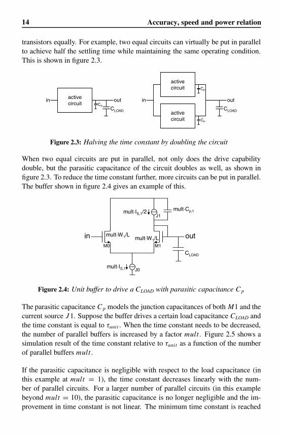
When two equal circuits are put in parallel, not only does the drive capabilitydouble, but the parasitic capacitance of the circuit doubles as well, as shown infigure 2.3. To reduce the time constant further, more circuits can be put in parallel.The buffer shown in figure 2.4 gives an example of this.
in out
CLOAD
mult·Cp,1
mult·W1/L mult·W1/L
mult·IS,1/2
mult·IS,1
M0 M1
J0
J1
Figure 2.4: Unit buffer to drive a CLOAD with parasitic capacitance Cp
The parasitic capacitance Cp models the junction capacitances of both M1 and thecurrent source J1. Suppose the buffer drives a certain load capacitance CLOAD andthe time constant is equal to τunit . When the time constant needs to be decreased,the number of parallel buffers is increased by a factor mult . Figure 2.5 shows asimulation result of the time constant relative to τunit as a function of the numberof parallel buffers mult .
If the parasitic capacitance is negligible with respect to the load capacitance (inthis example at mult = 1), the time constant decreases linearly with the num-ber of parallel circuits. For a larger number of parallel circuits (in this examplebeyond mult = 10), the parasitic capacitance is no longer negligible and the im-provement in time constant is not linear. The minimum time constant is reached
Accuracy, speed and powe r relation

15
0,00
0,01
0,10
1,00
1 10 100 1000 10000 100000
τunit(mult) [s]
mult
τmin
Figure 2.5: Simulation of the relative time constant as a function of thenumber of parallel buffers
when the parasitic capacitance is dominant over the load capacitor (see also equa-tion 2.17). This means that no speed improvement is achieved when the powerof the circuit is increased, since gm and Cp increase equally. In general, thismeans that for a power-efficient implementation the parasitic capacitance shouldbe smaller than the applied load capacitance, otherwise more than half of the out-put power of the circuit is consumed to drive its own parasitic capacitance. Theminimum time constant τmin which can be reached is independent of the appliedload capacitance CLOAD and is determined by the ratio of gm and Cp of the actualcircuit implementation.
2.5
Important parameters which determine the matching and the allowed signal swingare technology dependent. The required load as derived earlier in this chapter istherefore determined very much by the technology used. The parameters whichdetermine the required power and the minimum achievable settling time, such asthe current factor β , minimum gate length L and parasitic capacitances are alsodependent on the technology.
Minimum power scaling
The oxide breakdown voltage and therefore the oxide material and thickness de-termines the permitted supply voltage and achievable signal swing. In this sec-tion the scaling factor for the (effective) oxide thickness (tox) and minimum gatelength is assumed to be s. As a starting point, for a certain realization of a circuitin the 0.18 µm CMOS technology, s is set to one. s is smaller than one for more
CMOS technology trends
CMOS technology trends
2.5
□

16
advanced technologies. With the use of equations 2.6 and 2.11, equations 2.18and 2.19 derive the relative dependence of the minimum required capacitancefor a matching and a noise-limited design as a function of s. It is assumed thatAVT
[5], Cox and Vrms [8] are scaling with s and that NEF remains constant fordifferent technologies.
Cmatching = Cox
3
(AVT
σ (Voffset)
)2
∝ 1
s(2.18)
Cnoise = NEF kT
V 2noise,rms
∝ 1
s2(2.19)
Figure 2.6 shows the theoretical relative dependance of the minimum requiredcapacitance for different technologies.
Scaling factor s
Rel
ativ
e C
mat
chin
gch
ange
Rel
ativ
e C
nois
ech
ange
Scaling factor s
Figure 2.6: The relative capacitance dependence on the scaling factor s
The curve of Cmatching left side (for small s) is dashed, since it is dependenton technology parameters, which might not have the dependency on technology,as described above, for future technologies. As can be seen in figure 2.6, formatching- and noise-limited designs the capacitance increases with 1
sand 1
s2 re-spectively. To calculate the resulting power, it is assumed that the bandwidth (orthe required settling time) remains constant, that Vgt scales linearly with Vdd , andthat gm
Idsis inversely proportional to Vgt (for the chosen operation point where Vgt
is between 100 mV and 300 mV [8]):
P = Vdd · Ids
Ids∝Vgt · gm
gm∝Cx∝ Vdd · Cx
}Vdd∝s⇒ Px ∝ Cx · s2 (2.20)
In equation 2.20 Cx is Cmatching for a matching-limited design and Cnoise for anoise-limited design. Figure 2.7 shows the resulting relative power dependencefor a matching- and a noise-limited design as a function of the scaling factor s.
Accuracy, speed and powe r relation
□
□

17
Scaling factor s
Rel
ativ
e P
mat
chin
gch
ange
Rel
ativ
e P
nois
ech
ange
Scaling factor s
1Pnoise ∝sPmatching ∝
Figure 2.7: The relative power dependence on the scaling factor s forconstant bandwidth
Vgt cannot be scaled down infinitely with s. For small Vgt (near sub-threshold),gm
Idsis not inverse proportional to Vgt , but gm
Idsbecomes inversely proportional to√
Vgt [8]. In this case equation 2.20 changes into:
Ids ∝ √Vgt · gm ∝ √
Vdd · Cx ⇒ Px ∝ Cx · s32 (2.21)
Due to the non-linear relation between gm
Idsand 1
Vgtfor small Vgt the power becomes
approximately inversely proportional to the square root of s for a noise-limiteddesign, while it is proportional to the square root of s for a matching-limiteddesign. This is indicated in figure 2.7 with the dotted lines. This means that forlow accuracy, high-speed A/D converters it is advantageous to move into a moreadvanced technology, while a high-accuracy A/D converter, which is generallynoise limited, is more power efficient in an older technology (if the A/D converterarchitecture is kept constant).
An interesting situation occurs for advanced technologies (s < 1 in figure 2.7)when the supply voltage is kept constant and critical transistors are implementedin the most advanced, thin oxide transistors. The voltages on and between alltransistor terminals then have to be sufficiently small. The non-critical transistorsare implemented in thick-oxide technology. The critical transistors determine thegm. In this case, the noise capacitance shown in figure 2.6 does not change asa function of s, while the matching dependent capacitance is proportional to s,since the input signal amplitude can be maintained. Because Vdd and therefore Vgt
do not scale, the power for a noise-limited design will remain constant, but moreimportantly, the power for a matching-limited design will remain proportional tos. This, however, is not a standard design technique.
CMOS technology trends2.5

18
Maximum speed scaling
The parasitic capacitance determines the maximum achievable speed. Generally,the major contribution of the parasitic capacitance (Cp in figure 2.3) at the outputof a circuit comes from the drain junction capacitor. This drain junction capa-citance is relatively constant per unit width over several CMOS technologies [9].However, due to scaling with s, the minimum L scales with s, β scales with 1
s
and Vgt is scaled with s. Scaling of the quadratic equation for the drain currentresults in:
Ids = β
2· W
L· V 2
gt ∝ 1
s· W
ss2 ∝ W ∝ Cp (2.22)
It shows that Ids is proportional to the parasitic capacitance, regardless of thescaling factor s. Using the relation between gm
Idsand Vgt , the effect of scaling on
the minimum time constant τmin can be derived:
1
τmin
∝ gm
Cp
∝ gm
Ids
∝ 1
Vgt
∝ 1
s(2.23)
In equation 2.23 it is shown that the minimum time constant scales with s. Thismeans that when using a more advanced technology, the maximum achievablespeed is increased. In equation 2.23 it is assumed that Vgt is between 100 mVand 300 mV [8]. For smaller Vgt ,
gm
Idsis inversely proportional to
√Vgt . The
relation between τmin and s then becomes less than linear and the improvement inmaximum speed when the design is transferred to a more advanced technology isless than for designs with Vgt < 100 mV.
If the most advanced transistors are used while the supply voltage is kept constant,Vgt can also be kept constant. This results in τmin ∝ 1
s2 .
2.6 Conclusions
The minimum required capacitances in an A/D converter are determined by thenoise or the matching requirements. The minimum required capacitance fromboth the noise and the matching requirements are quadratically dependent on therequired accuracy, while the total capacitance is determined by the maximum ofthe capacitance from the noise or matching requirement. This maximum capacit-ance needs to be charged with the respective signal with sufficient accuracy withina certain time period, which is a measure for the power consumption. The totalrequired capacitance, the accuracy and the speed are A/D converter architecture
Accuracy, speed and powe r relation
□
□
19
dependent. This makes it possible to compare the power consumption of differentA/D converter architectures, as discussed in chapter 3.
This comparison can be made because the power consumption is proportional tothe load capacitance and inversely proportional to the available settling time, ifthe parasitic capacitor is smaller than the load capacitance. If the available set-tling time approaches its lower limit, which means that the parasitic capacitancereaches the load capacitance, the power consumption is no longer inversely pro-portional to the time constant, but increases dramatically.
In this chapter it is shown that in matching-limited designs it is beneficial to usethe most advanced technology. The decreasing power supply reduces the allowedsignal swing, however the matching parameter AVT
also decreases. For noise-limited designs, the input signal amplitude should be as large as possible, whichcalls for older technologies with larger supply voltages. The maximum speed isachieved in the most advanced technologies where the ratio between gm and theparasitic capacitance Cp generally increases.
The errors caused by matching errors can be reduced by using calibration tech-niques, which will be discussed in chapter 4. The capacitance resulting frommatching requirements can therefore be decreased. However since noise is a ran-dom process, it can not be calibrated and the capacitance determined by noiserequirements is the lower limit and can not be reduced by calibration.
2.6 Conclusions

Chapter 3
A/D converter architecturecomparison
3.1 Introduction
A number of different A/D architectures exist for a given set of specifications.This chapter describes the main known architectures and their limitations in termsof minimum required capacitance, power and speed. The architectures can bebroadly classified into parallel and serial structures. The former include flash,
signal is made by a number of parallel devices (i.e. comparators). The secondcategory includes pipe-line and successive approximation, where in general only
Sigma Delta, counting and (dual)slope A/D converters are not taken into account in this comparison, since onlywide-band or Nyquist converters are considered in this book.
The choice of technology is determined primarily by the application. There aretwo main possibilities in this respect. First is the class of stand-alone A/D convert-ers. For this class, the specifications to be achieved by the A/D converter determ-ine the technology. In this book the focus is on the second class, the embeddedapplications, where the analog part, which contains the A/D converter, needs tobe integrated with the digital circuits on a single chip. For systems with large di-gital processing this means that the A/D converter has to be designed in a CMOStechnology optimized for digital circuits. For example, the supply voltage in thiscase is reduced with newer technologies. A/D converters designed in CMOS tech-nologies optimized for digital circuits have an additional requirement. They needto be robust with respect to scaling. Newer digital CMOS technologies allow re-duction of the area of the digital circuitry, which is cost efficient. However, the
folding and two (or multi) step converter, where the decision about an input
21
one device is (re-)used to make the decision.

22
analog circuits, like A/D converters, also have to operate in this newer technology(with reduced supply voltage). The matching parameters for transistors, resistorsand capacitors that are determined by the technology are also very important inthe design of A/D converters. The basic A/D converter architectures are describedin this chapter, however publications about these architectures deal with morespecific solutions to ensure the greatest possible independence from the limitingprocessing parameters.
The different A/D converter architectures can be compared with each other withrespect to power efficiency because, together with the achieved accuracy andsampling speed, the efficiency of the architecture can be derived. In chapter 2 itis derived that the power is proportional to the capacitance that has to be charged.This capacitance is a function of the architecture. In the next sections the min-imum capacitance required to perform a proper conversion is derived from thearchitecture. This is called the intrinsiccapacitance Cintr . This capacitance can bedetermined by noise or matching requirements. Together with the speed requiredto charge this capacitance, the figure-of-merit of the architectures is derived, en-abling a proper comparison of the power efficiency for each architecture. This isdone in section 3.7. In the comparison the power required in the digital part of therespective A/D converter is ignored for the sake of simplicity.
The architectures that are compared in this chapter are integrated circuit, Nyquistconverters. These are:
• Flash
• Folding
• Two-Step / Subranging
• Pipe-line
• Successive approximation
Each section first describes the architecture and its accuracy-limiting componentsand from this the total intrinsic capacitance is calculated.
3.2 Flash
The most commonly known architecture is the flash A/D converter [10, 11, 12, 13,14]. This architecture has several implementation possibilities. First the full-flasharchitecture is considered, and then two enhancement techniques are described:interpolation and averaging.
A/D Converter architecture comparison
23
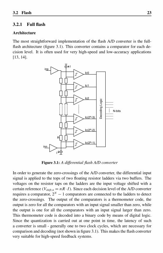
3.2.1 Full flash
Architecture
The most straightforward implementation of the flash A/D converter is the full-flash architecture (figure 3.1). This converter contains a comparator for each de-cision level. It is often used for very high-speed and low-accuracy applications[13, 14].
inn
Ic0
Ic1
Ic2
Ic(2N-3)
Ic(2N-2)
Ic(2N-1)
inp
Dec
odin
g Lo
gic
N-bits
I
I
R
Figure 3.1: A differential flash A/D converter
In order to generate the zero-crossings of the A/D converter, the differential inputsignal is applied to the tops of two floating resistor ladders via two buffers. Thevoltages on the resistor taps on the ladders are the input voltage shifted with acertain reference (Vshift,n = nR ·I ). Since each decision level of the A/D converterrequires a comparator, 2N − 1 comparators are connected to the ladders to detectthe zero-crossings. The output of the comparators is a thermometer code, theoutput is zero for all the comparators with an input signal smaller than zero, whilethe output is one for all the comparators with an input signal larger than zero.This thermometer code is decoded into a binary code by means of digital logic.Since the quantization is carried out at one point in time, the latency of sucha converter is small - generally one to two clock cycles, which are necessary forcomparison and decoding (not shown in figure 3.1). This makes the flash converter
Flash
very suitable for high-speed feedback systems.
3.2

24
Accuracy
Since each level of the flash A/D converter has to be detected with the accuracy ofthe overall converter accuracy, each comparator making this decision should havethis accuracy. The offset of the input stage of each comparator must therefore besufficiently low (section 2.2.1). The number of bits N which have to be resolvedby the A/D converter determines the accuracy of a decision level. In general,the accuracy of a decision level has to be within 1
4 of a least-significant bit (LSB)(appendix A) for a degradation of less than 2.4 dB in signal-to-noise and distortion(SINAD).
Intrinsic capacitance
The intrinsic capacitance, which consists of the capacitive load of the comparat-ors, is determined by two factors. The number of bits (N) of the A/D converterdetermines the number of comparators and the required comparator accuracy. Thenumber of comparators is 2N − 1. Since the offset voltage of the comparators isassumed to be a Gaussian distribution with zero mean and a standard deviationσ , the probability that all comparators of the flash converter are within a certainlimit can be calculated [1]. This probability corresponds to the yield of the A/Dconverter. The required σVoffset of a single comparator is a function of this requiredyield. The condition that all the comparators must have an offset smaller than 1
4 ofan LSB results in the following equation for the yield of an N-bit flash converter:
Yield =(
1 − P
(Voffset
σ>
LSB
4σ
))2N−1
(3.1)
The probability function P is in this case normalized to the standard normal dis-tribution N(0,1). This equation can be used to derive the demands for σVoffset if ayield of 0.99 is required, with a maximum offset of 1
4 of an LSB. Figure 3.2 shows
the required ratioσVoffset
VLSBto achieve a yield of 0.99, as a function of the number of
bits (N).
As can be seen in figure 3.2, the difference betweenσVoffset
VLSBfor N = 1 and N = 20
is only a factor two, while the difference between N = 1 and N = 20 in thenumber of comparators is already 220. Therefore, for the sake of simplicity for thecalculation of the intrinsic capacitance the maximum allowed comparator offsetvoltage is assumed to have a constant value of 0.0625, for all N , which equals14 of LSB
4 . The size of the input transistors is calculated using equation 2.6, with
A/D Converter architecture comparison

25
N [bits]
][ VLSB
Voffset −0.0625
VLSB
Voffset =
Figure 3.2: RequiredσVoffset
VLSBas a function of the number of bits (N) for a
yield of 0.99, with a maximum offset of LSB4
σVoffset = Vpp
4·4·2N = Vpp
2N+4 . The total intrinsic capacitance of these comparators canthen be calculated by:
Cintr,flash = (2N − 1) · Cdiff ,input,matching ≈ CoxA2VT
3V 2pp
· 23N+8 (3.2)
The total intrinsic capacitance is calculated in equation 3.2 assuming that the off-set of the comparators is only determined by the input transistors. In practice, thecircuitry after the input transistors also contributes to the offset, depending on theactual implementation. For the sake of simplicity, however, only the input tran-sistors are considered in this analysis. If the number of bits in a flash converter isincreased, the load increases by a factor of 8 for every extra bit. Figure 3.3 showsthe total load capacitance as a function of N .
From figure 3.3 the total intrinsic capacitance of the flash A/D converter canbe calculated. For example, for an 0.18µm technology: AVT
= 5 mV, Cox =2 and Vpp = 1 V, for a 10-bit converter the intrinsic capacitance is over
16 nF! Because of the large amount of comparators needed at the overall accur-acy, this capacitance is high for large N . Consequently, techniques to reduce theintrinsic capacitance of a flash A/D converter, like interpolation and averaging,have been developed. They are described in the next sections.
Flash3.2
7 fF/µm
□
□

26
N [bits]
10AC
VC 92Vox
2ppintr,flash
T
−⋅
~23N
3.2.2 Interpolation
Architecture
The required zero-crossings can be derived from the floating ladders directly asshown in figure 3.1. This requires 2N − 1 input pairs connected to the ladders.The 2N − 1 required zero-crossings can also be generated by interpolation [15] ofpre-amplifier outputs as shown in figure 3.4a.
The pre-amplifiers with gain A in figure 3.4a generate the zero-crossings of theladder taps. By taking the outputs of adjacent pre-amplifiers, additional zero-crossings are generated as shown in figure 3.4b. This interpolation substantiallydecreases the input capacitance seen at the ladder, since the number of input pairsis halved. The number of interpolation stages (Nint ) can be more than one. Whenseveral interpolating pre-amplifier stages are used (Nint > 1) instead of only onepre-amplifier stage, the number of input pairs connected to the ladders is reducedeven further. 2N − 1 comparators are still required for the quantization of the2N − 1 zero-crossings. When gain is applied in the interpolating pre-amplifierstages, however, the accuracy requirements of these comparators are reduced. Theintrinsic capacitance of the comparators is thus greatly reduced.
In practice, the transfer curve of a pre-amplifier is non-ideal. The active regionof the input of a pre-amplifier, consisting of a differential pair, is limited by thelimited linear region of this input transistor pair. When the linear region is notsufficient, the interpolated zero-crossings deviate from the wanted position [16].
A/D Converter architecture comparison
function of the number of bits (N)Figure 3.3: Total intrinsic capacitance of a flash A/D converter as a
[ ]–

27
o(x)
on(x)
o(x+2)
on(x+2)
o(x-2)
on(x-2)
on(x)
o(x)
o(x+2)
on(x+2)
Ic(x)
Ic(x-1)
Ic(x-2)
Ic(x+1)
Ic(x+2)
Ic(x)Ic(x+1)
Ic(x+2)
A
A
A
output [V]
input [V]
Figure 3.4: Interpolation of pre-amplifier outputs (a) and additional zero-crossing generation (b) for one interpolation stage (Nint = 1)
additional power is required for a sufficiently large linear region.
Intrinsic capacitance reduction
The gain factor A of each stage reduces the accuracy requirements of the sub-sequent stages. For the sake of simplicity it is supposed that the gain factor A isequal to A0 for all stages and the offset contribution referred to the input scaleswith A0 per interpolation stage. The intrinsic capacitance of one input pair ineach interpolation stage i can then be calculated as a function of the number ofinterpolation stages Nint :
Cintr,pair,i =(Nint
A0+ 1) · CoxA
2VT
3A2i0 V 2
pp
· 22N+8, (3.3)
for 0 ≤ i ≤ Nint . In figure 3.4a it can be seen that the input capacitance of onepre-amplifier is given by equation 3.3 for i = 0, while the input capacitance ofone comparator is given by equation 3.3 for i = 1 = Nint . With equation 3.3 thetotal intrinsic capacitance of an interpolated flash A/D converter can be calculatedas a function of Nint , by summing the intrinsic capacitances Cintr,pair,i of all theinput pairs in each interpolation stage:
Flash
(a) (b)
In this derivation it is assumed that the interpolation is ideal, which means that no
3.2
□

28
Cintr,flash interpolation =Nint∑i=0
(2N−(Nint −i) − 1)Cintr,pair,i
≈Nint∑i=0
2N−(Nint −i)Cintr,pair,i (3.4)
To calculate the effect of interpolation on the intrinsic capacitance of a flash A/Dconverter equation 3.4 is divided by equation 3.2:
Cintr,flash interpolation
Cintr,flash≈
Nint∑i=0
(Nint
A0+ 1
)· 2i−Nint
A2i0
(3.5)
This ratio is only dependent on the number of subsequent interpolation stages Nint
and the pre-amplifier gain A0. Equation 3.5 is plotted in figure 3.5 as a functionof A0, with Nint as a parameter.
A0
Nint
][ C
C
intr,flash
ioninterpolat intr,flash −
Nint = 1
Nint = 2Nint = 3Nint = 4
Figure 3.5: Improvement in intrinsic capacitance by using interpolationas a function of the pre-amplifier gain A0 with the interpola-tion factor Nint as a parameter
When Nint = 0 the ratio of equation 3.5 equals one, since this is the same asthe flash A/D converter without interpolation. This is independent of the gainA0, since there is no pre-amplifier stage. For Nint ≥ 1 and low gain A0, theA/D converter with interpolation has more intrinsic capacitance than the flash A/Dconverter without interpolation. The reason for this is that with interpolation morestages contribute to the offset with respect to the flash A/D converter, which causesa higher intrinsic capacitance. For larger gain A0, the effect of the gain is that the
A/D Converter architecture comparison
[ ]–
= 0 (= full flash)

29
stages after the first interpolation stage contribute less to the total input-referredoffset, resulting in a lower intrinsic capacitance. For the limit case, when the gainA0 becomes very high (∼10), only the first interpolation stage determines thetotal offset. Since the first stage consists of 2N−Nint − 1 stages with respect to 2N
stages in a flash A/D converter without interpolation, the maximum achievableimprovement is equal to ∼2Nint, which is the result of equation 3.5 for large A0.In practice, however, the A0 is limited by the achievable linear region of the pre-amplifiers and the achievable gain-bandwidth product. The pre-amplifiers need tobe linear for a sufficiently large input signal swing for proper interpolation.
From 3.5 we can conclude that already for moderate gain values (A0 ∼4) the im-provement in intrinsic capacitance is close to 2Nint . This improvement is causedby reducing the number of required accurate pre-amplifiers and therefore reducingthe intrinsic capacitance. When interpolation is used with only a small gain factor,for example for very high-speed converters [14], the total intrinsic capacitance isnot reduced. However, interpolation is beneficial, since at the input fewer ampli-fiers with high accuracy are required, which reduces the input capacitance of thefirst stage of the converter.
Interpolation reduces (under the condition of sufficiently high A0) the total in-trinsic capacitance of the A/D converter, but it does not reduce the mismatcheffects of each individual amplifier. The next paragraph describes a techniquewhich improves the overall A/D converter linearity without increasing the size ofthe input transistors.
3.2.3 Averaging
Architecture
Averaging [17, 18, 19, 14] is a technique which improves the overall linearityof the A/D converter by averaging the error of an individual amplifier with sev-eral neighboring amplifiers. This is achieved by sharing the outputs of adjacentpre-amplifiers by inserting averaging resistors. The pre-amplifiers with averagingresistors and the effects of these averaging resistors are shown in figure 3.6 [19].
Ideally, the relationship between input and output is a straight line, but because ofoffset errors (indicated by the open dots in figure 3.6a), a random pattern is shownaround the ideal curve as indicated by the thin lines connecting the open dots.The output resistors of the pre-amplifiers are indicated as the resistors between theopen dots and the black dots. The averaging resistors are connected between theblack dots. As can be seen, lowering this averaging resistor R2 pulls the curve toa straight line, which reduces the pre-amplifier offset effect. Increasing the outputresistances R1 of the pre-amplifiers also increases this effect. In fact the amount
Flash3.2

30
input [V]
digitaloutput
after averaging
R1 R2R1 R2
R1 R2R2
before averaging
Figure 3.6: Pre-amplifiers with averaging (a) and the effect of averagingon the transfer curve (b) [19]
of averaging is a function of the ratio R2R1
. Figure 3.7 shows the reduction of the
mismatch effect as a function of the ratio R2R1
in the case of an infinite pre-amplifierarray [14] and an infinite linear input range of the pre-amplifiers.
As can be concluded from figure 3.7, a smaller R2R1
ratio reduces the effect of mis-match of the pre-amplifiers. The first assumption in figure 3.7 is that the number ofpre-amplifiers is infinite. However, since the pre-amplifier array is not infinite inpractice, the R2
R1ratio cannot be reduced infinitely. This effect changes the position
of the zero-crossings of the pre-amplifiers at both ends of the array. The positions
However,unequally spaced reference voltages are undesirable for matching. A more accur-ate compensation is to apply out-of-range circuitry, such that the zero-crossingsof the in-range pre-amplifiers remain at their wanted position. By using an av-eraging termination circuit, which scales the resistors at both ends of the array,the required number of added over-range pre-amplifiers can be minimized. Theoperation of this termination circuit is described in [14]. The total number of out-of-range pre-amplifiers p required is a function of the ratio R2
R1and is described by
A/D Converter architecture comparison
(a)
(b)
the following equation:
that the zero-crossings after averaging are at their wanted position [14].of the zero-crossings can be restored by changing the reference voltages such

31
offset reduction [ ]
][ RR
1
2 −
Figure 3.7: Reduction in mismatch effect as a function of the ratio R2R1
,of an infinite pre-amplifier array and an infinite linear inputrange of the pre-amplifiers
p =√
1 + 8R1
R2− 1 (3.6)
For high order of averaging, more out-of-range pre-amplifiers are therefore re-quired, which increases the intrinsic capacitance.
The second assumption in figure 3.7 is the infinite linear range of the pre-amplifierinput stages. Since in practical realizations of pre-amplifiers the linear input rangeis limited, the amount of offset reduction of a certain pre-amplifier is limited bythe number of pre-amplifiers which are also in their linear input range. In general,the offset reduction after averaging is at maximum reduced by a factor
√Nlinear ,
where Nlinear is the number of pre-amplifier stages operating in the linear inputrange [19]. This is illustrated in the example where if the averaging resistance R2
is equal to zero, and for example 5 pre-amplifiers are in their linear input range,then these 5 pre-amplifiers can be seen as one lumped pre-amplifier, with a sizethat is 5 times larger. This reduces the mismatch with
√5.
Intrinsic capacitance reduction
Since the offset of the pre-amplifiers is reduced due to averaging, smaller devicescan be used in order to achieve the same accuracy. This reduces the intrinsic capa-citance (the total input capacitance of the pre-amplifier array). The reduction in in-
Flash
–
trinsic capacitance is calculated for an array of Npreamps (in-range) pre-amplifiers,
3.2

32
which is, for example, the input stage of the comparators in a flash A/D converter.This pre-amplifier array is shown in figure 3.8.
R1 R2R1 R2
R1 R2R1 R2
R1 R2R1R2
terminationpre-amps
terminationpre-amps
Figure 3.8: Pre-amplifier array, consisting of Npreamps pre-amplifiers
When averaging is applied to this array, which means that R2 < ∞, p (equa-tion 3.6) out-of-range pre-amplifiers have to be added in order to keep the zero-crossings at the wanted position. These additional pre-amplifiers have to be addedto the total Npreamps of the array. The resulting total intrinsic capacitance with re-spect to the total intrinsic capacitance of the reference pre-amplifier array can beexpressed as a function of the number of pre-amplifiers (Npreamps), the requiredout-of-range pre-amplifiers p and the offset reduction. The latter two are both afunction of R1 and R2.
Cintr,averaged array
Cintr,array (R2→∞)
=(Npreamps + p
(R2R1
))Npreamps
·(
offset red
(R2
R1
))2
(3.7)
The offset reduction (offset red) reduces the capacitance quadratically due to thequadratic relation between the capacitance and the required accuracy (2.2.1). Thereduction in intrinsic capacitance can be drawn as a function of the ratio R2
R1with
the number of pre-amplifiers Npreamps as a parameter.
As shown in figure 3.9, the maximum improvement which can be achieved equalsthe number of pre-amplifiers in the in-range part. The improvement can neverexceed this value since this is equal to the required size (and the respective in-trinsic capacitance) of one amplifier for sufficient matching. In this limit case theoffset of all the pre-amplifiers is averaged for each zero-crossing. The maximumreduction in intrinsic capacitance is therefore 1
Npreamps.
When more pre-amplifiers (Npreamps) are used, the reduction in intrinsic capacit-ance is larger, since more pre-amplifiers in their linear region contribute to theaveraging. For a certain value of R2
R1, for example 0.1, the reduction in capacitance
is larger for larger Npreamps . The reason for this is that the additional out-of-rangepre-amplifiers (p) are independent of Npreamps , but are relatively smaller for largerNpreamps . For a small R2
R1ratio the number of required out-of-range pre-amplifiers
becomes impractical since the reference range also has to increase. For example,
A/D Converter architecture comparison

33
][ C
C
)array(Rintr,
array averagedintr,
2
−∞→
Npreamps= 128
Npreamps= 64
Npreamps= 32
Npreamps= 8
Npreamps= 16
][ RR
1
2 −
Figure 3.9: Reduction in capacitance as a function of the ratio R2R1
, withthe number of pre-amplifiers Npreamps as a parameter
with equation 3.6 it can be calculated that for R2R1
= 0.1 the number of additionalpre-amplifiers is 8.
Due to its parallel signal processing, the flash A/D converter architecture is suit-able for high-speed conversion. However, this parallel processing also limits thepractical accuracy to 8 bits. Interpolation and averaging techniques reduce the in-trinsic capacitance, thus reducing the power consumption. These techniques canalso be combined [14].
3.3 Folding and interpolation
Architecture
For a higher number of bits it is obvious from figure 3.3 that the load of thecomparators of a flash A/D converter becomes significantly large. To reduce thenumber of comparators and the number of input stages, the folding and interpola-tion architecture can be used [20, 21, 22, 16, 23, 24]. By folding the input signal,the same comparators can be used for several parts of the total range. The numberof folds is called the folding factor Ff . Figure 3.10 shows one folding signal witha folding factor of 8.
However, the analog circuitry is not able to make the sharp transitions shown infigure 3.10. Nevertheless, between the transitions there is a linear region. Toensure linearity over the whole fine range a few parallel folding signals are
3.3 Folding and interpolation

34
input [V]
output [V]input
folded signalcomparatorlevels
Figure 3.10: Folding of input signal
input [V]
output [V]
folded signal 1
4 comparatorlevels
folded signal 2
4 comparatorlevels
Figure 3.11: Parallel folding by generating two folding signals
Instead of taking one folding signal with 8 detection levels (figure 3.10) it is alsopossible to use 2 folding signals shifted with respect to the input signal with 4 de-tection levels (figure 3.11) each. This can be expanded to 8 folding signals withone detection level each. However, generating these folding signals requires thesame amount of hardware as a full flash converter, since each zero-crossing isgenerated by one differential pair. To reduce the required number of differentialpairs, interpolation can be used to generate additional detection levels (or zero-crossings). Between the folding signals shown in figure 3.11 additional detectionlevels are generated by an interpolating resistor ladder [20, 22], as shown in fig-ure 3.12.
The number of additional interpolated levels is the interpolation factor (Fint ).For example, 16 detection levels can be generated with 4 folding amplifiers and4 times interpolation. The interpolation factor is limited by the requirement ofintegral non-linearity (INL). A larger interpolation factor requires a sufficientlyhigh linear region of the folding-amplifiers [16]. This is in contradiction with
’
A/D Converter architecture comparison
comparators.shows two parallel folding signals of which only the linear parts are applied to
linear’ part is used for conversion. Figure 3.11generated, of which only the

35
Folding amp
Folding amp
Folding amp
Folding amp
input
input [V]
output [V]
Figure 3.12: Interpolation of folding signals
proper folding which requires a small linear region, as will be explained later. Aninterpolation factor of 8 or 16 is often used [16, 19, 23]. For a proper conversionof the whole input range the different possible input voltages which correspondto the same folding output signal also have to be distinguished. This is done byconnecting the input signal directly to additional comparators which generate themost-significant-bits (MSBs) of the total A/D converter. The block diagram of thetotal folding A/D architecture is shown in figure 3.13.
Folding amp
Folding amp
Folding amp
Folding amp
input
Inte
rpol
atio
n
Com
para
tors
Com
p
Dec
oder
Data out
SHA
Figure 3.13: The folding and interpolation architecture
The sample-and-hold amplifier (SHA) at the input is required for high-frequencyinput signals because the folding pre-processing acts as an amplitude-dependentfrequency multiplier [16]. Since the folding and interpolating A/D architecturemakes its decision in one clock cycle, like the flash architecture it is very suitablefor high-speed applications.
Folding and interpolation3.3

36
Accuracy
The input signal is sampled by the SHA. The noise sampled in and generated bythis SHA directly influences the accuracy of the conversion. The accuracy of afolding architecture is mainly determined by the accuracy of the input transistorsof the folding amplifiers. The offset of these input pairs determines the INL of theconverter since this directly influences the positions of the zero-crossings. Theymust therefore have the accuracy of the overall A/D converter accuracy. Whensufficient gain in the folding amplifiers is applied the comparator offset require-ment is reduced by this gain. Other accuracy-determining factors are the size ofthe linear region of the folding amplifiers [16].
Intrinsic capacitance
When the input-referred offset of the folding amplifiers and the comparators isequally distributed, the total intrinsic capacitance of the folding amplifiers inputstage is calculated in a similar way to the flash A/D architecture:
Cintr, foldamps = 2N
Fint
· Cdiff ,input,matching = CoxA2VT
3FintV 2pp
· 23N+8 (3.8)
where Fint is the interpolation factor which is applied to the A/D converter andthe same yield conditions as in the flash architecture are considered. Because offolding, the number of required comparators is less than in the flash architectureand the gain in the folding amplifiers reduces the required comparator accuracy.The intrinsic capacitance from the comparators is calculated by:
Cintr, foldcomps = 2N
Ff
· Cdiff ,input,matching = CoxA2VT
3Ff Afa2V 2
pp
· 23N+8 (3.9)
where Ff is the folding factor and Afa is the gain of the folding amplifier. Ff
gives the number of times a comparator is reused in the total signal range. A lar-ger value means that fewer comparators are required, although the demand on thelinear region of the folding amplifiers increases. A small linear region is requiredbecause otherwise more than one differential pair influences a zero-crossing at theoutput of the folding amplifier. This problem can be solved by using transistorsin weak inversion to generate a small Vgt . To circumvent slow operation due tothe large accumulated junction capacitances at the output of the folding amplifiera trans-resistance amplifier is used [22]. Another solution is given by using cas-cading of the folding action [19]. This relaxes the Vgt demands but the numberof accurate input stages remains the same. The gain of the folding amplifiers Afa
A/D Converter architecture comparison
□
□

37
is limited by the limitation in linear region of the folding amplifiers, a large gaintogether with a large linear region will involve more power.
The total intrinsic capacitance of a folding A/D converter can be calculated bysumming the results of equation 3.8 and 3.9:
Cintr, folding = Cintr, foldamps + Cintr, foldcomps (3.10)
The result from equation 3.10 is shown in figure 3.14 as a function of N , with thefolding factor Ff and the interpolation factor Fint as a parameter.
N [bits]
Ff = 8 and 32, Fint = 8
Ff = 8, Fint = 16
Ff = 8, Fint = 32
10AC
VC 92Vox
2ppngintr,foldi
T
−⋅
~23N
Figure 3.14: Total intrinsic capacitance of a folding A/D converter as
f int
As can be seen in this figure, the folding factor does not influence the intrinsiccapacitance. This is caused by the fact that in this calculation the folding amplifiergain Afa is assumed to have a moderate value of only 4. The folding amplifierinput transistors are then dominant in the overall capacitance and the number ofcomparators hardly influences the intrinsic capacitance. The interpolation factor istherefore of greater importance. But doubling the interpolation factor only reducesthe number of input transistor pairs by half, which reduces the input capacitance of
In the comparison of the A/D converter architectures it will be made clear that theintrinsic capacitance of the SHA in a folding A/D converter is much less than the
parameter
Folding and interpolation3.3
[ ]–
flash A/D converter only by the interpolation factor (8-16).ting A/D converter architectures reduce the total capacitive load with respect to ament increases for a larger interpolation factor.of the dominating folding amplifiers only by half. And also the linearity require-
a function of the number of bits (N), with F and F as a
Generally, folding and interpola-

38
intrinsic capacitance due to matching requirements. It is therefore ignored in thecalculation of the total intrinsic capacitance of a folding A/D converter.
3.4 Two-step
By quantizing the analog signal in two steps, the number of comparators can bereduced significantly [25, 26]. A rough estimation determines in which part of therange the input signal lies and a more accurate quantization determines the digitalcode inside this part of the range. This section discusses the two-step architecture.A more general name is the subranging architecture, since more than two steps canalso be used for quantization [27].
Architecture
A two-step A/D converter divides the quantization into two steps [26]. First arough estimate is made with the coarse quantizer in the part of the range where theinput signal is. This information is used to subtract the coarse signal with a D/Aconverter from the input signal. The remaining residue signal is then quantized inthe fine quantizer to generate the LSBs. This is illustrated in figure 3.15.
input [V]
input
residue signalfinelevels
coarselevels
output [V]
Before the fine quantization is done, the residue signal is amplified by the residueamplifier to reduce the accuracy requirements in the fine A/D converter. Since thecoarse and the fine quantization do not take place at the same time, the use of asample-and-hold amplifier (SHA) is obligatory. The total two-step or subrangingarchitecture is shown in figure 3.16.
To make a proper conversion, first a settling phase is required for the coarse con-version and, following this, the signal has to be amplified and applied to the fine
A/D Converter architecture comparison
generate the residue signalFigure 3.15: Coarse levels determine the DAC subtraction levels to

39
CoarseADC
NC bitsDAC
FineADC
NF bits
DecoderRes
AMPSHA N bits
inputΣ+
Figure 3.16: Two-step A/D converter architecture
converter. This therefore requires twice the settling time with respect to the flashand folding and interpolating architecture, although the settling requirements dur-ing coarse conversion are relaxed with respect to the settling during fine conver-sion, as will be explained later.
Accuracy
The first component that determines the accuracy of the two-step converter is theSHA. Noise generated and sampled in the SHA deteriorates the analog input sig-nal which has to be quantized by the A/D converter. This generated and samplednoise has to be sufficiently low. To perform a proper total conversion the coarseA/D converter has to have an accuracy such that the resulting residue signal isalways in the range of the fine A/D converter. This means that the comparat-ors in the coarse A/D converter have to be accurate at the overall A/D converteraccuracy, which is N bit. An error made in the coarse conversion results in an out-of-range residue signal [28]. The coarse decision drives a D/A converter, whichgenerates an analog signal representing the coarse code. This D/A converter out-put is subtracted from the analog signal held by the SHA. It is obvious that thesignal generated by the D/A converter has to be N-bit accurate. But this does notcontribute to the power when the coarse references are used [28] and is thereforeomitted from the intrinsic capacitance calculation. The resulting residue signal isapplied to a residue amplifier. An offset in this residue amplifier results in shiftingthe residue signal within the fine range and causes the residue signal to be out-of-range in the fine A/D converter. The accuracy therefore needs to be the total A/Dconverter accuracy of N bit. The total offset error of the coarse A/D converter andthe residue amplifier need to be within one LSB of the total A/D converter. Thisis shown in figure 3.17.
If the residue signal remains within the grey area of figure 3.17, the transfer of thetotal A/D converter is always monotonic. This means that the coarse decision andthe offset of the residue amplifier always have to be within LSB
2 . The accuracyrequirements of the fine A/D converter are relaxed due to the gain of the residue
3.4 Two-step
−

40
LSB
residue signal
residue amplifier offset
coarse comparator offset
finelevels
input [V]
output [V]
Figure 3.17: Maximum allowed offset of both coarse A/D converter andresidue amplifier, indicated by the grey area
amplifier. The requirements of the fine comparators are the total A/D converteraccuracy divided by the gain of the residue amplifier.
Redundancy
The accuracy requirement of the subrange selection results in high demands on thecoarse A/D converter, as described above. When the coarse A/D converter makesan error, missing codes occur since the corresponding residue signal does not fitin the selected subrange. Figure 3.18a shows a proper subrange selection with itsoutput code. Figure 3.18b shows the effects of an incorrect subrange selection.
As can be seen in figure 3.18b, the errors in the coarse A/D converter cause theresidue signal to be out of range in the fine A/D converter. The coarse A/D con-verter accuracy requirements can be relaxed by using overlap of subsequent sub-ranges [29]. This means that additional comparator zero-crossings are presentoutside the fine A/D converter range. The result of these additional zero crossingsis that near a subrange transition a wanted code can originate from both subranges
A/D Converter architecture comparison

41
digitaloutput
input [V]
Fine range
input [V]
Fine range
Missing Codes
C(n) C(n+1) C(n+2) C(n) C(n+1) C(n+2)
digitaloutput
coarse comparator offsets
Figure 3.18: Residue signals resulting from a proper subrange selection(a) and errors due to coarse comparator offset when no sub-range overlap is used (b)
offsets on the overall transfer of the A/D converter when subrange overlap is used.
digitaloutput
input [V]C(n) C(n+1) C(n+2)
In-range
Under-range
Over-range
coarse comparator offsets
Figure 3.19: No subrange transition errors when subrange overlap is used
The digital encoding of the digital signals coming from the coarse and the fine A/Dconverter needs to resolve the errors from the coarse A/D converter. A schematicoverview of this is shown in figure 3.20.
The encoder needs to detect whether over- or under-range has occurred and onecoarse LSB is then subtracted or added to the coarse digital code accordingly.
3.4 Two-step
around this subrange transition. Figure 3.19 shows the effect of coarse comparator
(a)
(b)(a)

42
Coa
rse
A/D
Fin
e A
/D
If UR = 1 then,Coarse = Coarse – 1
If OR = 1 then,Coarse = Coarse + 1
Else Coarse = Coarse
Coarse*2NF + Fine
Output
ORUR
Figure 3.20: Digital decoding of over- and under-range occurrences
Redundancy1 is a very powerful optimization with respect to required accuracy.For example, when the fine range is doubled, the accuracy requirements of thecoarse A/D converter are reduced to half an LSB of this coarse converter, e.g. a 10-bit A/D converter with 5 coarse and 5 fine bits. Using half an additional subrangeon both sides increases the intrinsic capacitance of the fine A/D converter by 2,but reduces the load capacitance of the coarse A/D converter by a factor of 212!
Adding over-range to the fine A/D converter not only reduces the coarse A/Daccuracy, but also means the offset requirements of the residue amplifier can bereduced as well. Since residue amplifier offset causes a shift of the residue signalwithin the fine A/D converter range, this error can be traded-off with the error inthe subrange selection. Redundancy therefore reduces both A/D converter accur-acy and the residue amplifier offset requirement.
Generally, the accuracy of the fine A/D converter is increased by one bit. Com-pared to the bare minimum, a larger fine accuracy does not further reduce the re-quirements of the coarse A/D converter since then the monotonicity of the coarseA/D converter is not guaranteed.
Intrinsic capacitance
The coarse A/D converter accuracy and the residue amplifier accuracy are linkedtogether. If it is assumed that the over-range of the fine A/D converter is one bit,the sum of the error of the coarse A/D converter and the residue amplifier offset:
1 Redundancy can be used in all types of converters where a selection has to be made for the fol-lowing step. These are the pipe-lined, two-step and successive approximation (SAR) architectures,as explained later.
A/D Converter architecture comparison
Output =

43
Voffset,tot = Voffset,res amp + Voffset,crs comp
= Voffset,res amp + x · Voffset,res amp, (3.11)
with x = Voffset,crs comp
Voffset,res amp, is allowed to be half an LSB of the coarse A/D converter
resolution. In this case the over-range of the fine A/D converter is able to correctthese errors. With the use of equation 2.6 the total offset is expressed in thecapacitance of the input of the residue amplifier stage:
Voffset,tot ∝ 1√Cres amp
+ x√Cres amp
(3.12)
When equation 3.12 is rewritten, the total capacitance of both the coarse A/Dconverter and the residue amplifier stage can be expressed in x, Voffset,tot and thenumber of coarse bits NC:
Ctotal = Cres amp + 2NC · Ccrs comp
∝√
x + 1
Voffset,tot+ 2NC · 1
x2
√x + 1
Voffset,tot(3.13)
By minimizing equation 3.13, the optimum value for the ratio x between the offsetof the coarse comparators and the residue amplifier results in:
x = Voffset,crs comp
Voffset,res amp= 1
2NC
3
(3.14)
In the derivation above it is assumed that the coarse A/D converter consists of afull flash converter without enhancement techniques as interpolation or averaging.It is obvious that a different coarse A/D converter influences this ratio. Using theratio of equation 3.14, the intrinsic capacitance of the residue amplifier can beexpressed as a function of the number of coarse bits NC :
Cintr,res amp =(
1 +√
22NC
3
)2
· CoxA2VT
3V 2pp
· 22NC+8 (3.15)
The part after the brackets is the intrinsic capacitance required for a maximum ofLSB
4 offset error. The part between the brackets is the result of an optimum distri-bution of the offset errors over the coarse conversion and the residue amplifier (see
3.4 Two-step
□

44
equation 3.14). The intrinsic capacitance of the coarse A/D converter is calculatedin a similar way to the flash architecture (equation 3.2). With the only differencethat the accuracy of the coarse decision is dependent on the ratio of equation 3.14:
Cintr,crs ADC =
(1 +
√2
2NC3
)2
22NC
3
· CoxA2VT
3V 2pp
· 23NC+8 (3.16)
The accuracy of the fine A/D converter is chosen LSB4 (appendix A), since the
fine conversion determines the positions of the quantization levels contrary to thecoarse conversion, which only selects the proper subrange. The offset require-ment is divided by the gain of the residue amplifier, which is in general equal tohalf of the number of levels of the coarse A/D converter (2NC−1) since the signalapplied to the fine A/D converter consists of two subranges due to redundancy.The intrinsic capacitance of the fine A/D converter is then:
Cintr,fine ADC = CoxA2VT
3V 2pp
· 23N−3NC+12 (3.17)
Cintr,res amp, Cintr,crs ADC and Cintr,fine ADC are dependent on NC . The optimum valueof NC can be calculated by minimizing the sum of these capacitances. The op-timum value of NC can be approximated by:
NC,opt ≈ N + 1
2(3.18)
The total intrinsic capacitance resulting from the matching requirements in a twostep A/D converter is the sum of equation 3.15, 3.16 and 3.17:
Cintr match,twostep = Cintr,res amp + Cintr,crs ADC + Cintr,fine ADC (3.19)
Figure 3.21 shows the total capacitance of the two-step architecture and the
C (equation 3.18), as a function
In figure 3.21 the coarse and the fine A/D converters are based on the full flashA/D converter without enhancement techniques. If these techniques, such as inter-polation or averaging, are applied to these stages, the total capacitance is reducedsignificantly, since the intrinsic capacitance from the residue amplifier, which isnot reduced by such enhancement techniques, is not dominant in the total intrinsicmatching capacitance.
A/D Converter architecture comparison
contributions separately with optimum value for N
of N .
□
□

45
N [bits]
][ 10AC
VC 92Vox
2ppintr
T
−⋅ −Cintr match,twostep~21.4N
Cintr,res amp
Cintr,crs ADC
Cintr,fine ADC
Figure 3.21: Total intrinsic matching capacitance of a two-step A/D con-verter as a function of the number of bits (N) and the separatecontributions for optimum NC
The SHA which is required at the input of the two-step architecture (figure 3.16comprises a capacitor to hold the analog signal during the hold phase. Duringsampling, in addition to the input signal thermal noise is also sampled onto thiscapacitance. The amount of thermal noise is calculated by equation 2.12. Thissampled thermal noise has to be sufficiently low, as explained in section 2.2.2,to achieve an accuracy of N bits. When a buffer drives this capacitance (sec-tion 2.2.2), the required hold capacitance is given by:
Cintr,SHA = 8 · 22N+2NEF kT
V 2pp
, (3.20)
with NEF as the noise excess factor [7]. Equation 3.20 can be drawn as a functionof the number of bits N . This is shown in figure 3.22.
The sum of the values derived from figure 3.21 and figure 3.22 is the total in-trinsic capacitance of a two-step A/D converter. The intrinsic capacitance origin-ating from the sample and hold capacitance is small with respect to the intrinsicmatching capacitance. For example, in 0.18 µm CMOS, with AVT
= 5 mV,Cβ
ox = 7 fFµm2, Vpp = 1 V, NEF = 4 and N = 12, the total intrinsic matchingcapacitance is 35 pF, while Cintr,SHA is 13 pF. The coarse and fine A/D convertersare dominant in the total capacitance for accuracies up to 12 bits. This capacitancecan be reasonably reduced by architectural enhancements. However, when boththe coarse and fine flash A/D converters are optimized by using the techniquesdescribed in section 3.2, this difference becomes smaller. For higher accuraciesthe intrinsic capacitance from the SHA can even become dominant.
3.4 Two-step

46
N [bits]
]V[pF VC 22ppSHAintr, ⋅
~22N
Figure 3.22: Total intrinsic capacitance of a SHA in a two-step A/D con-verter as a function of the number of bits (N), with NEF = 4
The two-step architecture provides a large reduction in intrinsic capacitance com-pared to the flash architecture. However, to make a proper conversion, it is veryimportant in a two-step structure that the fine range fits exactly in a coarse range.In this derivation above it is assumed that the circuitry that provides this guaranteehas a negligible contribution to the intrinsic capacitance. In the next chapter of thisbook architectural changes are presented to deal with these range and gain topics.In the two-step architecture the coarse and the fine quantization take place withinone clock period. The next section describes the pipe-line architecture where thequantization operations take place serially.
3.5 Pipe-line
Architecture
The pipe-line architecture [29] shows a large similarity to the two-step architec-ture. A two-step A/D converter consists of 2 stages, while a pipe-line A/D con-verter generally consists of N stages, each including a SHA, an A/D converter,a D/A converter, a subtractor and an amplifier. The difference between the two-step and the pipe-line architecture is the SHA after each stage. The conceptual
The basic operation is the same as in the two-step architecture. The first stagesamples the analog input signal. This signal is converted to the digital domainto estimate the held input. The result from this quantization is applied to theD/A converter, which generates an analog signal that represents the digital A/D
A/D Converter architecture comparison
one-bit-per-stage pipe-line is shown in figure 3.23.

47
SHA1-bitADC
1-bitDAC
AmpΣ+
Stage 1 Stage NStage iInput
Figure 3.23: Pipe-line A/D converter architecture with one bit per stage
input signal. This produces the residue signal, which is amplified before it isapplied to the next stage. Contrary to the two-step architecture the second stagethen samples this amplified residue signal and the same operations take place.This is continued until all stages have performed their conversion. All digitaloutput values are combined to generate the digital output code. Due to the pipe-lining concept (caused by the inserted SHAs) the first stage can start samplinga new analog input signal while the second stage processes the previous sample.The speed of the conversion is therefore determined by the speed of a single stage.The drawback of this, however, is a larger latency. Figure 3.23 shows the case forone bit per stage, although more configurations are possible, such as one and ahalf bits per stage to resolve A/D converter errors [29] or a first stage with threebits and the remaining stages with one and a half bits per stage [30]. First the oneand a half bit first stage is considered and then the advantages with respect to adecreasing total intrinsic capacitance are described.
One and a half bits per stage relaxes the demands on the comparators (inside theADC in figure 3.23) since it adds redundancy, but does not change the require-ments for the capacitors in the SHA with respect to noise or absolute residue gainrequirements. Since the capacitors in the SHAs are dominant in the total intrinsiccapacitance, for the sake of simplicity the conceptual one bit per stage pipe-line
During a conversion cycle, first the signal is sampled and a conversion is per-formed. Subsequent to that the DAC has to be set with the proper code and thesubtraction has to be carried out. Within one clock cycle there are therefore twosettling actions that have to be performed, as in the two-step architecture.
A = 2
converter output. The D/A converter output is subtracted from the held analog
discussion.converter is considered, while the comparator requirements are left out of the
3.5 Pipe-line
–

48
Accuracy
The accuracy of the pipe-line architecture is determined mainly by two factors.The noise sampled in each pipe-line stage reduces the achievable SNR of theconverter. The one (and one and a half) bit per stage pipe-line architectures relyon the exact factor of two gain in each stage. This also puts constraints on thematching of capacitors. First the origin of noise is discussed.
In each stage of the pipe-line converter the analog signal is re-sampled. Thismeans that in each stage all of the wide-band noise generated in the switches andbuffers of that stage is folded back into the sampling base-band. Due to the gainafter each pipe-line stage, the contribution to the total noise of the last stages isless than the contribution of the first stages (referred to the input). Since the noisepower generated in each stage is inversely proportional to the load capacitance(equation 2.8), the required capacitances can be scaled. For example, the scalingfactor can be chosen such that the contribution in noise is equal for all stages.This, however, causes the power to be dominated by the first stage [31]. For theconceptual pipe-line A/D converter (without parasitic capacitances) the optimumscaling factor is two for the subsequent stages [31]. This means that the first stagecontributes the same amount of noise as the sum of all the remaining stages.
The gain factor of two is critical in the performance of the pipe-line architecture.This is equal for both the one bit or one and a half bit per stage architecture sinceredundancy does not solve gain errors. Generally, this gain factor is determined bythe ratio of two capacitors. Due to capacitor mismatch [32, 33] this gain factor candeviate from its ideal value, which causes INL errors. The capacitor mismatch isarea dependent. Larger capacitors have better matching. The total intrinsic capa-citance is determined by the largest capacitance determined by noise or matching.
For the one bit per stage A/D converter shown in figure 3.23 decision-accuratecomparators are required. However, when redundancy is applied (as in the two-step converter) the accuracy requirements of the comparators are reduced. Sincethe sampling capacitors are dominant in the total intrinsic capacitance, the com-parators are left out of the calculation.
Intrinsic capacitance
In this section first the minimum required capacitance for noise considerations iscalculated, then the matching of capacitors is discussed.
Due to re-sampling in each stage, the noise requirement can be considered sep-arately for each stage. In this derivation it is assumed that for each stage there is
A/D Converter architecture comparison

49
actions per stage, the required capacitance is two times larger. The contribution tothe total noise of each stage is chosen such that the capacitance of a certain stagehas the same value as the sum of the capacitances of all subsequent stages [31].In this case the first stage produces half of the total noise. When a buffer drivesthis capacitance (section 2.2.2), the total required capacitance in this case can becalculated by (equation 2.8):
Cintr,pipeline,noise,1 = 2 · 8 · 22N+2NEF kT
V 2pp
(3.21)
For the remaining stages the capacitance is scaled down by a factor of two. Therequired capacitance per stage as a function of the number of bits is then given by:
Cintr,pipeline,noise,i =(
2
2i−1
)8 · 22N+2NEF kT
V 2pp
(3.22)
the total intrinsic capacitance required for noise considerations can be calculatedby summing the capacitances of all the stages:
Cintr,pipeline,noise =N∑
i=1
Cnoise,pipeline,i = 2N+7(2N − 1
)NEF kT
V 2pp
(3.23)
The total intrinsic capacitance (equation 3.23) can be drawn as a function of thenumber of bits N . This is shown in figure 3.24.
N [bits]
~22N]V[pF VC 22
ppnoisepipeline,intr, ⋅
one sampling action [34]. When a pipe-line scheme is chosen with two sample
3.5 Pipe-line
with i as the stage number (1 ≤ i ≤ N). For an N-bit pipe-line A/D converter
function of the number of bits (N), with NEF = 4Figure 3.24: Total capacitive load of a pipe-line A/D converter as a

50
In this figure NEF from equation 3.23 is assumed to be four. As can be seen infigure 3.24, the capacitive load grows exponentially with the required accuracy.
To calculate the matching requirements of the capacitors it is assumed that thefollowing relation exists between the error due to mismatch in capacitance andthe value of the capacitance [32, 33]:
σC
C= AC√
C(3.24)
This equation supposes that an error in the capacitance is caused by fluctuationsin the thickness of the inter-metal layer. AC is a technology constant, dependenton the quality of the processing of the inter-metal layer. For example, in a doublepoly process the inter-poly oxide thickness is well controlled and therefore AC
is generally smaller than in the case of back-end capacitors. A general pipe-linestage is shown in figure 3.25.
in
C1
Aref
C1
C2
A
C2
+ +
out out+ +
Figure 3.25: A general pipe-line stage during sample phase (a) and holdand gain phase (b)
In the case of one bit per stage, the signal is sampled on capacitors C1 and C2
during the sample phase. During the hold and gain phase the charge of C1 istransferred to C2, which is then put in feedback. To ensure a gain of two, bothcapacitors shown in figure 3.25 have to have a ratio of C1
C2= 1. The maximum
error in the first stage, which results in a DNL (differential-non-linearity) errordue to a mismatch between C1 and C2, normalized to an LSB is given by:
DNL = �C1 · 2N−1
C1(3.25)
with �C1 = 4σC1 = 4AC · √C1. Rewriting equation 3.25 gives the minimum re-
quired input capacitance of the first stage for sufficient matching (equation 3.26).
Cintr,pipeline,match,1 = C1 + C2 = 2 · 22N+6A2C (3.26)
A/D Converter architecture comparison
–
– –
–
(a) (b)

51
The maximum allowed DNL is set at LSB4 . For sufficient yield, the maximum
allowed capacitance error has to be within σC
4 . As with the total capacitance cal-culated for the noise limitation, the same rule of scaling can be applied for calcu-lating the intrinsic capacitance for matching of the complete pipe-line converter.
Cintr,pipeline,match = 2N+8 (2N − 1
)A2
C (3.27)
The ratio between Cintr,pipeline,match and Cintr,pipeline,noise determines whether theintrinsic capacitance is determined by the noise or by the matching of capacitors.This ratio is given by:
Cintr,pipeline,match
Cintr,pipeline,noise
= 2A2CV 2
pp
kT · NEF(3.28)
It can be observed that this ratio is independent of the resolution (N). This meansthat the ratio holds for all of the stages inside a pipe-line converter. When theratio from equation 3.28 is smaller than 1, the intrinsic capacitance is determinedby the noise requirements and is calculated with equation 3.23. A ratio largerthan 1 means that the intrinsic capacitance is determined by the matching of thecapacitors and is calculated with equation 3.27 or calibration is required. Thisis described in the next chapter. Figure 3.26 shows the ratio as a function of thecapacitance matching parameter of a certain technology. This ratio is dependenton the signal amplitude and the NEF.
AC [√pF]
[ ]22ppnoisepipeline,intr,
matchpipeline,intr, VV
NEFC
C⋅
Vpp = 1 V,NE F = 4
Figure 3.26: The ratio of capacitor matching and noise requirements asfunction of the capacitance matching parameter AC
3.5 Pipe-line
requirements:This gives the following result for the total intrinsic capacitance for matching

52
From figure 3.26 it can be read that for Vpp = 1 V and a noise excess factor of
NEF = 4, the required capacitor matching is equal to AC = 91 pF12 . When for a
certain technology this matching is not achieved, the capacitors have to be scaledup for sufficient matching or calibration can be used to calibrate the gain factorof the respective stages. In [33] it is shown that when using a multi-bit first stagein a pipe-line A/D converter, the capacitor matching of the technology used issufficient and no increased capacitance or calibration is required.
Multi-bit first pipe-line stage
Using a multi-bit first pipe-line stage reduces the requirements and the intrinsiccapacitance of the subsequent stages [30, 35, 33, 36, 37]. As is shown above andin [31], the optimum scaling factor for the capacitances of succeeding stages isequal to the gain of the preceding stages.
equation 3.21 and equation 3.22, is then:
Pnoise,tot,onebit = kT
Cintr,pipeline,noise,1·(
2 − 1
2N−1
)(3.29)
When the pipe-line is implemented with a multi-bit first stage, the capacitor of thenext stage can be scaled with the gain of the first stage, which is generally 2NC ,where NC is the first stage resolution. The next stages are again scaled with afactor of two. This means that the total noise contribution of all the stages afterthe first stage is reduced by a factor of two for each additional bit in the first stage.The total thermal noise is then given by:
Pnoise,tot,mltbit = kT
Cintr,mltbitpipeline,noise,1·(
1 − 1
2N−2− 1
2NC−1
)(3.30)
For equal thermal noise, this means that the ratio between the intrinsic capacitanceof the first stage of a multi-bit pipe-line and a one-bit pipe-line is equal to:
Cintr,mltbitpipeline,noise,1
Cintr,pipeline,noise,1= 1 − 1
2N−2 − 12NC−1
2 − 12N−1
(3.31)
The total intrinsic capacitance of both the one-bit-per-stage and the multi-bit firststage pipe-line can be expressed in their respective first stage capacitances:
Cintr,pipeline,noise =(
2 − 1
2N−1
)· Cintr,pipeline,noise,1 (3.32)
A/D Converter architecture comparison
a-half bits) per stage this factor is two. The total thermal noise, calculated withIn the case of one bit (or one-and-
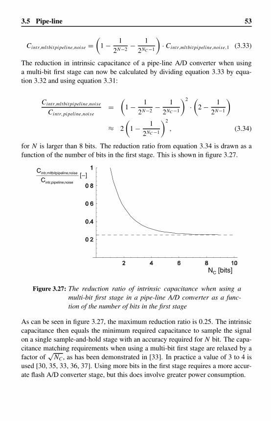
53
Cintr,mltbitpipeline,noise =(
1 − 1
2N−2− 1
2NC−1
)· Cintr,mltbitpipeline,noise,1 (3.33)
The reduction in intrinsic capacitance of a pipe-line A/D converter when usinga multi-bit first stage can now be calculated by dividing equation 3.33 by equa-tion 3.32 and using equation 3.31:
Cintr,mltbitpipeline,noise
Cintr,pipeline,noise
=(
1 − 1
2N−2− 1
2NC−1
)2
·(
2 − 1
2N−1
)
≈ 2
(1 − 1
2NC−1
)2
, (3.34)
for N is larger than 8 bits. The reduction ratio from equation 3.34 is drawn as afunction of the number of bits in the first stage. This is shown in figure 3.27.
NC [bits]
][ C
C
noisepipeline,ntr,i
noiseline,mltbitpipeintr, −
Figure 3.27: The reduction ratio of intrinsic capacitance when using amulti-bit first stage in a pipe-line A/D converter as a func-tion of the number of bits in the first stage
As can be seen in figure 3.27, the maximum reduction ratio is 0.25. The intrinsiccapacitance then equals the minimum required capacitance to sample the signalon a single sample-and-hold stage with an accuracy required for N bit. The capa-citance matching requirements when using a multi-bit first stage are relaxed by afactor of
√NC , as has been demonstrated in [33]. In practice a value of 3 to 4 is
used [30, 35, 33, 36, 37]. Using more bits in the first stage requires a more accur-ate flash A/D converter stage, but this does involve greater power consumption.
3.5 Pipe-line

54
3.6 Successive approximation
The pipe-line architecture uses a separate stage for each bit (in the one-bit-per-stage configuration). The successive approximation architecture uses the samequantization stage for each bit [38, 39, 40].
Architecture
The successive approximation A/D converter converts the analog signal to a di-gital code by a binary search. The SAR converter, shown in figure 3.28, consistsof a SHA, which has to hold the signal during the binary search.
SHA
D/A converter
input
Decision Register
Decision Logic
Pointerclock
Figure 3.28: Successive approximation A/D converter architecture
At the start of this binary search, the MSB of the D/A converter is set to one.All the other bits are set to zero. The (only) comparator decides whether theinput signal is larger or smaller than the signal from the D/A converter. After thisdecision, the MSB of the D/A converter is set according to this decision and theMSB 1 is set to one. Again the comparator compares the input signal to this newD/A converter value. This binary search continues until all bits have the propervalues. A conversion cycle is illustrated in figure 3.29.
The subtraction D/A converter can consist of a reference ladder with switches toselect the reference closest to the input signal level. However, for large resolution(>8 bits) a large amount of switches is required. The subtraction D/A convertercan also be based on charge redistribution [38, 40], which is done with capacitors.This, however, requires sufficient matching of capacitors.
A/D Converter architecture comparison
–

55
2
Vpp
4
Vpp
voltage
t
input
Sample input
N-times quantization cycle
1 total conversion cycle (N+1)
Sample input
Figure 3.29: Binary search of the output code
As can be seen in figure 3.29, a full conversion cycle takes an input sample timeplus N times a comparator decision cycle. In general this means that the conver-sion cycles of a SAR A/D converter has to be N + 1 times faster than the flasharchitecture to achieve the same Nyquist frequency. During the conversion cyclesredundancy can be applied, which relaxes both the accuracy and timing demandsof the quantization. The major power-consuming component in the SAR architec-ture is therefore generally the SHA. To optimize the power consumption a largerpart than 1
N+1 of the total sample period can be used for sampling the analog in-put signal. This means that the input sample time and the quantization cycles infigure 3.29 are not equally distributed over the full conversion cycle time. For thesake of simplicity, in the remainder of the calculation equal distribution (as shownin figure 3.29) is assumed.
Accuracy
As with the pipe-line architecture, both noise and capacitor matching are import-ant for the accuracy. The noise generated (or sampled) in the SHA needs to besufficiently low for the required accuracy, which is similar to the SHA of the two-step architecture. The D/A converter generally uses capacitors [38] (the samecapacitors as in the SHA [40]) to generate the proper subtraction signals. Thematching between the capacitors used in this subtractor determines the achievableaccuracy of the SAR converter. The comparator accuracy is not important, sincea comparator offset does not contribute to a conversion error. It only adds to theoffset of the overall SAR converter.
3.6 Successive approximation

56
Intrinsic capacitance
The capacitance in the SHA has to fulfill the noise requirements for a given num-ber of bits N . This is calculated with the same formula as for the two-step con-verter (equation 3.20). However, if the matching of capacitors of the technologyused is not sufficient for the given technology, the intrinsic capacitance has to beincreased and is given by equation 3.26. Equation 3.28 can be used to verify thematching of the capacitors used.
The intrinsic capacitance of the SAR architecture is therefore very similar to thatof the pipe-line converter. The difference is that the intrinsic capacitance of theSAR architecture is a factor of two less because there is only one stage. Theintrinsic capacitance determined by the noise requirement as a function of theresolution (N) is shown in figure 3.30.
N [bits]
]V[pF VC 22ppSARintr, ⋅
Figure 3.30: Total capacitive load of a SAR A/D converter as a function ofthe number of bits (N), with NEF = 4
Depending on the capacitor matching of the technology used, the intrinsic capa-citance shown in figure 3.30 has to be multiplied by the ratio shown in figure 3.26.
3.7 Theoretical power consumption comparison
In the previous section the theoretical minimum total capacitive load has been de-rived for several architectures. These results can be used to compare the efficiencyof the architectures as a function of the required number of bits N and the samplerate.
A/D Converter architecture comparison

57
3.7.1 Figure-of-Merit (FoM)
The FoM is calculated by dividing the power consumption of the A/D converterby the achieved accuracy and the minimum of the sample frequency and two timesthe resolution bandwidth (ERWB). This is explained with the aid of figure 3.31and given in equation 3.35.
ENOB
fin2
fs
ENOB,DCENOB,DC-0.5
fENOB,DC-0.5
Relevant for FoM
FoM = P
2ENOB,DCMIN(fs, 2fENOB,DC−0.5)(3.35)
The FoM is a measure for the required power per achieved resolution per con-version. Today, the state-of-the-art FoM for Nyquist A/D converters is around1 pJ/conversion, which means that 1 pJ per conversion cycle is required to convertan analog signal to a single bit.
3.7.2 Architecture comparison as a function of the resolution
Theoretical A/D converter comparison
Since the power consumption is proportional to the intrinsic
The intrinsiccapacitance determined by matching and noise is dependent on different techno-logy parameters. To be able to make a comparison between the architectures,
Figure 3.31: Representation of the figure of merit (FoM)
described earlier.Equation 3.35 is used for an objective comparison between the architectures
capacitance 2.15, in the calculation the calculated intrinsic capacitance for eacharchitecture is used as a measure for the power P in equation 3.35.
3.7 Theoretical power consumption comparison

58
realistic values for these technology parameters have to be chosen. To comparethe figure-of-merits therefore, as an example the technology parameters are set atvalues for a 0.18 µm technology. Those values are: Vpp = 1 V, Cox = 7 fF/µm2,AVT
= 5 mV and NEF = 4. However, this comparison can also be made for othertechnologies.
In the calculation of the intrinsic capacitance for each architecture the maximumallowed static error is set at LSB
4 (appendix A). The error of the signal on thecapacitor is not only determined by the static error, but is also a function of thesignal shape and the settling error that is causing a dynamic error. The signal shapeis considered to be a continuous analog signal (at the input of the A/D converteror a settling signal which is at maximum a full scale (Vpp) voltage step. Thebandwidth requirements of these signals are considered to be equal (section 2.3).To guarantee a total error of LSB
4 , an optimum distribution can be made betweenthe static and the settling error. The required power, when increasing the demandson the static error, is in general a quadratic function of the accuracy increment,while increasing the demands on the settling error is only a weak (logarithmic)function of the accuracy increment. Most of the allowed error of LSB
4 is thereforeassigned to the static error and the additional power required to reduce the settlingerror is ignored in the architecture comparison.
It assumed that the converters are able to handle signal frequencies up to theNyquist frequency. This means that in equation 3.35 fs of the respective A/Darchitecture is used. Since not all of the different architectures use a full sampleperiod for signal settling, a normalization factor (xNF ) is needed for equal datarate. The flash and folding architectures use a full sample period to drive the cal-culated intrinsic capacitances. The two-step and pipe-line architectures only havehalf a sample period available to drive the respective capacitances. This means
SAR architecture the available settle time is dependent on the number of bits. TheSAR architecture requires one cycle for tracking and N cycles for quantization.The normalization factor therefore equals N + 1. The normalization factors xNF
for each architecture are summarized in table 3.1.
The achieved ENOB at DC from equation 3.35 is assumed to be equal to 2N foreach architecture. As a reference, the capacitance required for sampling a signal atN-bit accuracy is chosen. This intrinsic capacitance is given by equation 3.20 andhas a normalization factor of one. For the architecture comparison the followingequation is used:
A/D Converter architecture comparison
the total sample period and the normalization factor equals two. In the case of thethat the settle time available to charge the intrinsic capacitances is only half of
□

59
Flash
Folding
Two step
Pipe lined
SAR
1
1
2
2
N+1
Architecture xNF
Table 3.1: The different A/D architectures with their normalizing factors xNF
FoMarch x
FoMref SHA= Cintr,x · xNF
Cintr,ref SHA(3.36)
The result of the comparison is shown in figure 3.32. The reference sample rate ischosen such that the calculated intrinsic capacitance dominates over the parasiticcapacitances.
Flash f int fa
Two-step
Pipelined, 1 bit 1st stageSAR
][ FoMFoM
SHA
X −
Pipelined, 4 bit 1st stage
Reference SHA
Figure 3.32: The figure-of-merit of different architectures relative to the in-trinsic capacitance of a single sample-and-hold as a functionof the number of bits N for
’
low’ sample rates
From figure 3.32 it can be seen that without enhancing techniques the flash archi-tecture is the least power-efficient architecture. This is due to the large amountof parallelism of this architecture. For each quantization level an accurate com-parator is required. The folding and interpolation architectures reduce the powerefficiency by reducing the required number of accurate input transistors by inter-
3.7 Theoretical power consumption comparison
polation. Also the number of comparators and their accuracy is reduced, by both
Folding, F = 8, N = 16, A = 4
N [bits]

60
folding and folding amplifier gain, respectively. From this figure it is clear thatthe power of a SHA is negligible in a folding A/D converter. Because of the re-duction in both the number of comparators and the accuracy requirement of thosecomparators by employing residue signal gain, the two-step architecture is able toincrease the power efficiency much further. The pipe-line architecture has a FoMwhich remains flat over the whole accuracy range. The intrinsic capacitance ofthe pipe-line is 8 times larger than the intrinsic capacitance of the single referencesample-and-hold. When the number of bits in the first stage is 4, the total intrinsiccapacitance is only 2 times larger. The SAR architecture has a smaller intrinsiccapacitor, although the available settling time is much smaller than the settlingtime of the pipe-line architecture.
From figure 3.32 it can be concluded that making sufficient gain just after the firststage results in the best architectures in terms of power efficiency.
Figure 3.32 shows the FoM of the architectures when no enhancement techniquessuch as interpolation, averaging or offset calibration are used. These enhancementtechniques reduce the intrinsic capacitances and therefore increase the power ef-ficiency. For example, when averaging is applied to the flash architecture, reduc-tion of intrinsic capacitance and thus of FoM of as much as a factor of 16 can beachieved. The same holds for the two-step architecture, the FoM of which can beoptimized by reducing the capacitive load of both the coarse and fine convertersand the residue amplifier, by averaging, interpolation techniques or calibration.This holds for accuracies below 14 to 16 bits, since above these accuracies theintrinsic capacitance is dominated by the sampling capacitor. The FoM of bothSAR and pipe-line architectures in figure 3.32 cannot be optimized further byenhancement techniques, since they are determined by the noise requirements.
This comparison is made using the technology parameters of a 0.18 µm techno-logy. Since for high accuracies the intrinsic capacitance of the two-step, pipe-lineand SAR architectures are determined by the noise requirements, the differencebetween these architectures remains the same for different technologies. For lowaccuracies, the intrinsic capacitances of the flash, folding and two-step architec-tures are determined by matching requirements. Since for more advanced tech-nologies the required capacitance for matching decreases faster than the requiredcapacitance for noise (section 2.5), the curves of these architectures will decreasewith respect to the other architectures.
A/D Converter architecture comparison

61
A/D converter comparison of realizations
The FoM of realized A/D converters can also be calculated and compared. How-ever, in the FoM calculated by equation 3.35 the input signal amplitude is notconsidered, while it is obvious from equation 2.6 and equation 2.12 that the in-put signal amplitude quadratically influences the intrinsic capacitance and thusthe power. Optimizing the input signal amplitude to the highest achievable valuetherefore greatly influences the required power. To be able to compare the real ar-chitecture efficiency, the FoM of equation 3.35 is normalized to Vpp = 1 V inputsignal amplitude, which was also the case in figure 3.32:
FoMVpp = P · V 2pp
2ENOB,DCMIN(fs, 2fENOB,DC−0.5)(3.37)
Tables 3.2 through 3.7 show the FoM calculated with equation 3.35 and the FoMnormalized to Vpp = 1 V using equation 3.37 of realized and published A/D con-verters from 1998 until 2004. Each table is sorted with the lowest FoMVpp on top.The realized A/D converters are distributed over the categories: flash, folding,
architecture, when in the realized two-step/subranging architecture re-sampling isalso applied (for example [27]). In this comparison the realized converter is put inthe two-step category if all of the two (or more) steps consist of more than threebits.
Table 3.2: Table of realized flash A/D converters
Ref N ENOB fs ERBW P FoM Vpp FoMVpp
[MS/s] [MHz] [mW] [pJ] [V] [pJV 2][41] 6 5,2 22 11 0,48 0,59 0,64 0,24[42] 7 6,1 450 80 50 4,56 0,8 2,92[14] 6 5,7 1500 500 328 6,31 1,2 9,09[43] 6 5,2 400 200 150 10,20 1 10,20[44] 6 5,8 500 160 225 12,62 1 12,62[45] 6 5,5 700 136 187 15,19 1 15,19[13] 6 5,6 900 450 300 6,87 1,5 15,46[46] 6 5,2 1300 750 545 11,41 1,6 29,20[47] 6 5,5 75 37,5 110 32,41 1 32,41[48] 8 7,1 200 50 655 47,75 1,3 80,69
The results of the calculation of the FoM normalized to Vpp = 1 V (FoMVpp)from the tables 3.2 through 3.7 and the ENOB dependency of the FoMVpp of the
3.7 Theoretical power consumption comparison
two-step/subranging, one-bit-first-stage pipe-line, multi-bit-first-stage pipe-line andSAR. It is difficult to distinguish between the pipe-line and two-step/subranging

62
Table 3.3: Table of realized folding A/D converters
Ref N ENOB fs ERBW P FoM Vpp FoMVpp
[MS/s] [MHz] [mW] [pJ] [V] [pJV 2][49] 8 7,5 1600 800 1270 4,38 0,8 2,81[24] 10 9,2 40 20 65 2,76 1,6 7,07[50] 8 7,5 600 400 200 1,84 2 7,37[51] 8 6,7 125 62,5 110 8,46 2 33,86[52] 8 7,7 10 5 76 36,55 1 36,55[53] 7 6,4 300 70 200 16,92 1,6 43,31
Table 3.4: Table of realized two-step/subranging A/D converters
Ref N ENOB fs ERBW P FoM Vpp FoMVpp
[MS/s] [MHz] [mW] [pJ] [V] [pJV 2][27] 14 12 100 50 1250 3,05 2 12,21[54] 8 7,6 100 50 118 6,08 1,6 15,57[55] 10 9,7 20 10 75 4,51 2 18,03[56] 12 10,3 50 25 850 13,48 1,6 34,52[28] 10 9,1 25 12,5 195 14,21 1,6 36,39[57] 13 11,1 40 15 800 12,15 2 48,60
Chap 7 16 10.8 20 2 141 19.7 2 79.1[58] 12 10,3 54 4 295 29,25 1,8 94,77
reference sample-and-hold capacitance are plotted in figure 3.33, with the realizedENOB on the x-axis.
From figure 3.33 it can be seen that the flash architecture is (barely or) not used atall for accuracies above 8 bits. This architecture is not suitable for high accuraciesbecause of the large intrinsic capacitance required. However, for low accuracies itcan be favorable to use interpolation and offset compensation techniques to reducethe intrinsic capacitance which optimizes the efficiency, which is shown by [41].
The realizations of the folding architecture show better efficiency than the realizedflash architectures, as expected from the intrinsic load capacitances. The realiza-tion described in [24] shows a good efficiency. This is the result of the use of aBiCMOS technology, which has better matching properties, resulting in a lowerintrinsic capacitance.
The realized FoMVpp of the two-step or subranging architectures is relatively con-stant for different values of the ENOB. In figure 3.32 it was shown that the FoMVpp
of a two-step converter increases less rapidly than the noise-limited architectures.Furthermore, because the two-step architecture is matching limited, calibration
A/D Converter architecture comparison

63
Table 3.5: Table of realized pipe-line A/D converters
Ref N ENOB fs ERBW P FoM Vpp FoMVpp
[MS/s] [MHz] [mW] [pJ] [V] [pJV 2][59] 10 9,2 220 100 135 1,15 1 1,15[60] 8 6,9 4000 800 4600 24,07 0,25 1,50[61] 8 6,5 20000 2000 9000 24,86 0,25 1,55[62] 10 8,7 140 70 123 2,11 1 2,11[63] 10 8,7 20 10 20 2,40 1 2,40[64] 10 9 30 15 16 1,04 1,6 2,67[65] 10 9,2 100 50 180 3,06 1 3,06[66] 10 8,7 30 15 16 1,28 1,6 3,28[34] 10 9,4 14,3 4 36 6,66 0,8 4,26[67] 10 9,4 80 40 69 1,28 2 5,11[68] 8 7,6 500 250 950 9,79 0,75 5,51[69] 15 12 20 8 233 3,56 1,5 6,97[70] 12 11,1 20 10 250 5,69 2 22,78[71] 12 10,8 10 5 338 18,96 1,6 48,53[72] 12 10,9 61 2,5 600 62,80 1,4 123,09[73] 14 12 20 10 720 8,79 4 140,63[74] 14 12,8 5 1 320 22,44 4 358,97
Table 3.6: Table of realized pipe-line A/D converters with a multi-bitfirst stage
Ref N ENOB fs ERBW P FoM Vpp FoMVpp
[MS/s] [MHz] [mW] [pJ] [V] [pJV 2][33] 14 12 75 37,5 341 1,11 2 4,44[36] 14 11,9 75 37,5 340 1,19 2 4,74[75] 12 50 23 780 4,14 1,2 5,96[76] 8 7,5 150 80 71 2,61 1,6 6,69[37] 12 11 75 37,5 290 1,89 2 7,55[30] 10 9,5 40 20 70 2,42 2 9,67[35] 12 11,3 65 32,5 480 2,93 2 11,72[77] 14 11,9 10 15 112 2,93 2 11,72[78] 15 11,7 40 19 394 3,12 2,25 15,78[79] 12 11 105 52,5 850 3,95 2 15,81
can be applied to reduce the intrinsic capacitance. This is discussed in the nextchapter.
As can be seen in figure 3.33, the FoMVpp of the pipe-line converter increases as afunction of the realized ENOB. The slope of the line through the realizations with
3.7 Theoretical power consumption comparison

64
Table 3.7: Table of realized SAR A/D converters
Ref N ENOB fs ERBW P FoM Vpp FoMVpp
[MS/s] [MHz] [mW] [pJ] [V] [pJV 2][80] 9 8,2 0,15 0,03 0,03 1,70 0,5 0,43[81] 8 7,7 0,1 0,045 0,0046 0,25 1,4 0,48[82] 8 7,2 20 10 12,9 4,39 1 4,39[83] 13,5 13 0,016 0,001 0,15 9,16 2,4 52,73[84] 12 11,5 0,125 0,0625 16 44,19 4 707,11
Flash
Folding
Two-stepSubranging
Pipe-line1 bit 1st stage
SAR
Pipe-lineMulti-bit 1st stage
ENOB,DC
FoMVpp[V2pJ/conv]
~ FoMref SHA~ 22ENOB
chapter 5
chapter 6chapter 7
0,10
1,00
10,00
100,00
1000,00
4 6 8 10 12 14 16
Figure 3.33: The figure of merit normalized to Vpp = 1 V of realized A/Dconverters and the slope of a reference SHA as a function ofthe achieved ENOB
low FoMVpp is equal to the slope of the FoMVpp of the reference sample-and-holdcapacitance. This is also equal to the expected slope shown in figure 3.24. Theconverters on this line are designed with capacitors, limited by the noise require-ments. Calibration does not reduce the capacitance in noise-limited designs. Theuse of a multi-bit first stage does, however, reduce the intrinsic capacitance withrespect to the one-bit first stage pipe-line converter, as is shown in figure 3.33.
An exception to this is the realization presented in [69], where a pipe-line A/Dconverter with a one-and-a-half-bit first stage achieves almost the same efficiency
A/D Converter architecture comparison

65
as the pipe-line A/D converters with a multi-bit first stage. This is a remarkableresult.
The SAR architecture is also a noise-limited design. This is shown in figure 3.33by the increasing FoMVpp as a function of the ENOB.
The result of the comparison of the realized A/D converters is not exactly equalto the theoretical result shown in figure 3.32. This is caused by the fact thatthe result from figure 3.32 shows the bare minimum achievable FoMVpp , whilethe realized FoMVpp depends very much on the actual implementation. However,figure 3.33 confirms the theory derived from figure 3.32 that for higher accuracies,the realizations of the two-step/subranging or pipe-line with multi-bit first stageA/D architectures are most efficient with respect to the other architectures. Forhigh accuracy the number of levels and the associated gain of the first stage haveto be large for high efficiency. In this case the dominant error source with respectto noise and matching is the first stage. After this first stage the contributions ofthe errors to the overall error are greatly reduced.
An important observation from figure 3.32 is that the FoM is not independent of theaccuracy for a given architecture, but increases for higher accuracy. This is causedby the fact that the capacitive load of the capacitance determined by both noise andmatching increases with 22N , while the achieved accuracy only increases with 2N .
3.7.3 Architecture comparison as a function of the sampling speed
Figure 3.32 shows the differences between the architectures for low sample rates.When the power is increased, indicated by mult in figure 2.5, the available settletime decreases by the same amount, allowing an increase of the sample rate. Whenthe power and sample rate are increased simultaneously, the FoM remains con-stant. However, when mult reaches the value where the available settle time doesnot decrease linearly with mult , the power increases more rapidly than the samplerate. This means that the FoM increases and the converter becomes less power ef-ficient.
This available settling time is used differently for the several A/D converter archi-tectures. As can be seen in table 3.1, the flash and folding architectures requireonly one settle period for one conversion cycle. The maximum achievable samplerate is therefore equal to 1
ts,min, where 1
ts,minis determined by the minimum achiev-
able time constant τmin (section 2.4). The two-step/subranging and pipe-line ar-chitectures use two settle periods within one conversion cycle, which results in amaximum sample rate of 1
2ts,min. The SAR architecture requires N + 1 settle peri-
ods for one conversion cycle, resulting in a maximum sample rate of 1(N+1)ts,min
.Non-idealities, such as necessary switching time in the two-step, pipe-line and
3.7 Theoretical power consumption comparison

66
SAR architectures or non-overlapping clock generation, which require part of thetotal sampling period, are not taken into account. This effect reduces the max-imum achievable sample rate of these architectures even further.
3.8 Conclusions
In this chapter the most important A/D converter architectures for high speed andhigh bandwidth are compared with respect to power consumption and maximumachievable speed. From the combination of figure 3.32 and the maximum achiev-able sample rates it can be concluded that for low sample rates the architectureswhich reduce the number of necessary accurate devices are much more powerefficient than the parallel type of converters like the flash and the folding architec-tures. This is especially the case for high accuracies, where the size of the intrinsiccapacitance of the flash and folding architecture becomes impractical. However,for high sample rates parallel architectures are more power efficient since the con-version is carried out in only one step.
Practical realizations also show the trend that for a high sample rate the flashand folding are the optimum architectures. However, due to the parallelism, theaccuracy is limited to 8/10 bits. For the higher accuracies two-step/subrangingand pipe-line with multi-bit first stage architectures are more efficient.
Designing for high accuracy requires some kind of calibration. When more bitsare applied in the first stage, the accuracy of the generation of the least significantbits becomes less critical. Generating more bits in the first stage(s) thus reducesthe calibration to only this stage. This is in contrast to the more parallel type ofarchitecture where all the decision blocks need calibration separately.
Because of its power efficiency for high resolution, the two-step architecture isfurther analyzed in the remainder of this book. The next chapter discusses
A/D Converter architecture comparison
enhancement techniques for this architecture to increase the accuracy withoutincreasing the power consumption, thereby increasing the power efficiency.

Chapter 4
Enhancement techniques fortwo-step A/D converters
4.1 Introduction
In the previous chapter the two-step architecture was chosen for further investiga-tion. This chapter first discusses the error sources in a two-step architecture. Themajor accuracy challenge in the two-step architecture is the need for an accurategain factor between the quantization stages to fit the residue signal exactly in thefine sub-range. In [3] an architectural solution for this requirement is provided,which is explained in section 4.3. Due to this solution, the offset of the residueamplifier stage becomes very important. Section 4.4 gives an overview of the ex-isting offset calibration methods as they are applicable on different A/D converterarchitectures. In section 4.5, a solution for background on-line digital offset ex-traction and analog compensation is discussed.
4.2 Error sources in a two-step architecture
Figure 4.1 shows the general diagram of the two-step architecture (section 3.4).Added to this figure are the main error sources which can limit the performanceof the two-step architecture.
Each of the error sources shown in figure 4.1 will be discussed and solutions areprovided in order to limit the performance reduction. The sample-and-hold is notconsidered since the requirements of this block in the two-step architecture arenot different from the requirements in other architectures.
67

68
SHA Coarse ADC DAC Fine ADCΣ Amp
εreference εcoarse quantization εsubtraction, εoffset
εgain, εoffsetεfine range, εfine quantization
input
error sources
• The coarse quantization determines the selection of the subranges and theDAC setting. When an error is made in this quantization (εcoarse quantization),the wrong subrange is selected, which results in missing codes, as shownin figure 3.18. By adding over-range to the fine A/D converter (section 3.4)the accuracy requirements of the coarse A/D converter are reduced signific-antly.
• The references of the D/A converter are important since they determine theaccuracy of the total A/D converter. An error in the references (εreference)results in an INL error. The reference therefore determines the accuracy ofthe overall A/D converter. In general, the matching of resistances providedin CMOS technology is sufficient [85, 86] for more than 12-bit accuracyand is adequate for the scope of this book.
• The subtraction of the input signal and the D/A converter output determinesthe overall achievable accuracy. An offset or a gain error in the subtraction(εsubtraction) results, for example, in an INL error. The consequences of theseerrors are similar to those of the errors made in the residue amplifier, whichwill be described later.
• The residue amplifier is an important accuracy-determining element of thetwo-step architecture. An offset (εoffset) on the residue amplifier or on thesubtractor gives a DC shift of the fine A/D converter reference with respectto the coarse A/D and D/A converter range. When over-range is applied inthe fine A/D converter (section 3.4), this offset can be larger than withoutover-range. However, an error in the gain factor of the residue amplifier(εgain) is much more critical [87]. A gain error in the cascade of the sub-tractor and the residue amplifier causes the total range of residue signal,which is the result of the subtraction of the input signal and the D/A con-verter signal, not to fit in the fine A/D converter range. This may lead tonon-monotonicity or missing codes [87]. The next section (4.3) discussesan architectural solution to overcome this limitation.
Enhancement techniques for two-step A/D converters
Figure 4.1: Diagram of the general two-step architecture with the possible
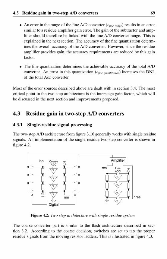
69
• An error in the range of the fine A/D converter (εfine range) results in an errorsimilar to a residue amplifier gain error. The gain of the subtractor and amp-lifier should therefore be linked with the fine A/D converter range. This isexplained in the next section. The accuracy of the fine quantization determ-ines the overall accuracy of the A/D converter. However, since the residueamplifier provides gain, the accuracy requirements are reduced by this gainfactor.
• The fine quantization determines the achievable accuracy of the total A/Dconverter. An error in this quantization (εfine quantization) increases the DNLof the total A/D converter.
Most of the error sources described above are dealt with in section 3.4. The mostcritical point in the two-step architecture is the interstage gain factor, which willbe discussed in the next section and improvements proposed.
4.3 Residue gain in two-step A/D converters
4.3.1 Single-residue signal processing
The two-step A/D architecture from figure 3.16 generally works with single residuesignals. An implementation of the single residue two-step converter is shown infigure 4.2.
Digital
Amplifier
inn
inp
res
nres
CoarseADC
FineADC
Figure 4.2: Two step architecture with single residue system
The coarse converter part is similar to the flash architecture described in sec-tion 3.2. According to the coarse decision, switches are set to tap the properresidue signals from the moving resistor ladders. This is illustrated in figure 4.3.
4.3 Residue gain in two-step A/D converters

70
input
residuesignals
inn inp
res
nres
Figure 4.3: Residue signal generation in a single residue system (with aresidue amplifier gain of 1)
For illustration purposes the residue amplifier gain in figure 4.3 is set at 1. Inpractice the gain is higher than 1. These residue signals are applied to a differentialamplifier, which applies its output to two resistor ladders which generate the finebits similar to the coarse converter. The amplitude of the residue signals, res andnres, applied to the fine ladders is determined by the resistance of a coarse tap, thecurrent in the coarse ladder and the gain of the residue amplifier.
The range of the fine A/D converter is determined by the current in and the resist-ance of the resistor ladders of the fine converter. Due to deviations in one of theelements mentioned above, ranging errors in the fine converter are easily made.Figure 4.4b shows the errors which occur when the gain of the residue amplifiersis less than expected.
The bold lines, res and nres, are the signals which are applied to the tops of bothresistor ladders. Because the gain of the residue signals is too low, the signal istoo small for the fine range. This can be seen at the beginning and at the end ofa subrange in figure 4.4b. This misfit causes jumps in the transfer curve of thetotal A/D converter at the subrange transitions, which leads to missing codes ornon-monotonicity. To circumvent this source of errors several precautions canbe taken. For example, if the fine range matches the full-scale residue amplifieroutput signal swing, which means that the references for fine converter experience
Enhancement techniques for two-step A/D converters
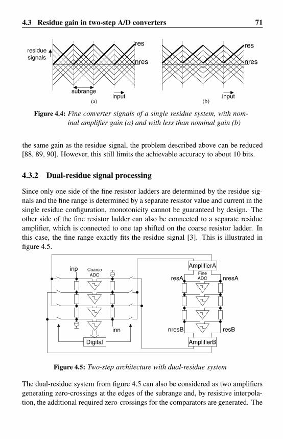
71
input input
residuesignals
res
nres
res
nres
subrange
Figure 4.4: Fine converter signals of a single residue system, with nom-inal amplifier gain (a) and with less than nominal gain (b)
[88, 89, 90]. However, this still limits the achievable accuracy to about 10 bits.
4.3.2 Dual-residue signal processing
Since only one side of the fine resistor ladders are determined by the residue sig-nals and the fine range is determined by a separate resistor value and current in thesingle residue configuration, monotonicity cannot be guaranteed by design. Theother side of the fine resistor ladder can also be connected to a separate residueamplifier, which is connected to one tap shifted on the coarse resistor ladder. Inthis case, the fine range exactly fits the residue signal [3]. This is illustrated infigure 4.5.
Digital
AmplifierA
inn
inp
AmplifierB
nresB resB
resA nresA
CoarseADC Fine
ADC
Figure 4.5: Two-step architecture with dual-residue system
The dual-residue system from figure 4.5 can also be considered as two amplifiersgenerating zero-crossings at the edges of the subrange and, by resistive interpola-tion, the additional required zero-crossings for the comparators are generated. The
4.3 Residue gain in two-step A/D converters
(a) (b)
the same gain as the residue signal, the problem described above can be reduced

72
switches are connected in such a way that, when switching from one subrange intothe next subrange, one amplifier remains connected to the coarse ladders, whilethe other amplifier changes two tap positions [91]. With this improved switch-ing, even with amplifier errors as described later, continuity and monotonicity areguaranteed. As a result of not only driving the top side, resA and nresA, of thefine reference ladders, but also the bottom side, resB and nresB, from the coarseresistor ladder, the range of the fine A/D converter is made directly dependent onthe selected coarse subrange and the amplifier gain. If in this case the gain of bothresidue amplifiers is reduced, it does not result in an error of the fine conversion.This is due to the fact that the fine range is dependent on the gain of the residueamplifiers. This is illustrated in figure 4.6.
input input
residuesignals
resB
nresBresA
nresA
resB
nresBresA
nresA
As can be seen in figure 4.6, the zero-crossings of the fine comparators remainat the same position, independently of the gain. The absolute gain of the tworesidue amplifiers is therefore not important. However, a lower residue amplifiergain increases the accuracy demands on the fine conversion. A difference in gainbetween the residue amplifiers causes the zero-crossings of the fine comparatorsto deviate from the ideal value. This effect is shown in figure 4.7.
As can be seen in figure 4.7a, the interpolated zero-crossings are shifted with re-spect to the ideal value and this causes an error in the transfer of the A/D converter.The maximum error in the INL curve from figure 4.7b can be calculated by:
INLmax,fine =√
GR − 1√GR + 1
· 2NF , (4.1)
with GR = AA
AB, the gain ratio of the gain of amplifier A and amplifier B and
NF is the number of bits of the fine A/D converter. By rewriting equation 4.1the maximum relative gain error |GR,max − 1| can be calculated. Assuming
(a) (b)
amplifier gain (a) and with less than nominal gain (b)Figure 4.6: Residue signals of a dual-residue system, with nominal
Enhancement techniques for two-step A/D converters

73
residuesignals
input
INL INLmax
input
Figure 4.7: Residue signals of a dual-residue system, with different gainfor both amplifiers (a) and the respective INL (b)
GR,max =(2NF +2 + 1
)2
(2NF +2 − 1
)2 (4.2)
In figure 4.8 the maximum relative gain error as a function of the required numberof bits NF in the fine A/D converter is shown.
NF [bits]
(∆GR,max–1) [%]
Figure 4.8: Maximum relative gain error as a function of the accuracy
The gain matching requirement is exponentially dependent on the number of bitsin the fine converter. When, for example, the fine A/D converter has to resolve8 bits (NF = 8), the required gain matching of the two residue amplifiers has
This matching is achieved by the intrinsic matching of
(figure A.1), then the maximum relative gain error is given by:that the maximum allowed INL is LSB
4 = 12NF +2 for less than 0.4 loss in ENOB
(a)
(b)
4.3 Residue gain in two-step A/D converters
to be better than 0.4%.

74
matching is required.
Another point for attention is the offset between the two residue amplifiers. Due tomismatch, the zero-crossings of the residue amplifiers can be shifted with respectto the wanted position. A difference between the offsets of the residue amplifiersresults in an INL error. This is illustrated in figure 4.9a.
residuesignals
input
INL INLmax
offset
input
Figure 4.9: Effect of residue amplifier offset on fine A/D converter zero-crossings (a) with the respective INL (b)
As can be seen in figure 4.9b, the INL curve follows a continuous line and therewill be no large code transitions due to the dual residue signal processing in thecase of amplifier offset. This is a result of interpolation between the two residueamplifier outputs, which determine the outer ends of the range. This means thatthe offset is spread over the whole range, the maximum DNL is therefore thedifference between the input-referred offsets of both amplifiers divided by theresolution of the fine A/D converter (equation 4.3). The maximum INL, however,is equal to this offset difference (equation 4.4).
DNLmax =∣∣∣∣Voffset A − Voffset B
2NF
∣∣∣∣ (4.3)
INLmax = ∣∣Voffset A − Voffset B
∣∣ (4.4)
To achieve an INL better than ±0.25 LSB, the difference in the amplifier offsethas to be within ±0.25 LSB.
the technology. The gain values of the amplifiers have to be calibrated if more
(a)
(b)
Enhancement techniques for two-step A/D converters

75
4.3.3 Conclusions
Dual-residue signal processing [3] is a powerful technique to circumvent rangingerrors which occur when the coarse subranges, residue amplifier gain and finerange are not coupled to each other. When improved switching is used, continu-ity and monotonicity are guaranteed. Dual-residue signal processing spreads theerrors of the amplifiers over the whole fine range, which results in an improvedDNL, and no missing codes will occur. A gain error is also spread over morecodes instead of causing missing codes. However, the difference in offset of thetwo residue amplifiers determines the INL of the overall A/D converter. For highaccuracy this means that the input devices of the amplifier need to be large toensure a sufficiently low offset. The next sections deal with offset calibrationtechniques, which allow the use of small input devices to improve the power andspeed of the converter.
4.4 Offset calibration
4.4.1 Introduction
In the single residue architecture, the offset of the residue amplifier is not critical.The over-range of the fine A/D converter is able to compensate the offset error.When dual-residue signal processing is used in a two-step architecture the offsetof the two residue amplifiers determines the INL, as described in the previoussection. The offset of the residue amplifier stage needs to be calibrated in orderto prevent the use of large input devices1 . This section describes a number ofcalibration techniques which can be applied to the two-step architecture.
4.4.2 Calibration overview
The offset of residue amplifiers in two-step converters, or in general in the criticalblocks of A/D architectures, can be calibrated in order to reduce the intrinsic capa-citance, thus reducing the required power. These critical blocks are, for example,
1Another option could be to calibrate the gain of a single residue system instead of the offset ina dual-residue system. However, in this book offset calibration is chosen over gain calibration sinceoffset can be measured and compensated more easily because it is a DC effect.
4.4 Offset calibration

76
the comparators or the amplifier stages. The calibration can be performed at sev-eral
’
moments’ during the lifetime of an A/D converter, as shown in figure 4.10.
Production Start-up Operation
Calibrationduring
production
Off-lineself-
calibration
Calibrationin
clock-cycle
Calibrationusing
output data
Generation ofadditional
calibration time
Figure 4.10: Calibration moments during the lifetime of A/D converters
These
’
moments’ occur during fabrication (testing), at start-up or continuouslyduring operation. Depending on when this
’
moment’ occurs, additional hardwareor calibration time, etc., is needed. These calibration schemes can be carried outeither in the analog or in the digital domain. The following paragraphs describethe different possibilities and their advantages and limitations.
Calibration during production
The most straightforward method of calibration is carried out off-line during fab-rication. When this method of calibration is used the process needs a type of pro-gramming facility on-chip, like laser-trimming or -cutting, or read-only memory(ROM) programming. These values are used for compensating the errors in theanalog or in the digital domain.
• A current D/A converter which is used for generating the references in, forexample, a two-step A/D converter can be calibrated by adjusting each ofthe separate current sources to their wanted value. This can be done byusing additional compensation D/A converters for generating the compens-ation current [92, 27]. These compensation D/A converters are programmedduring fabrication, for example by laser cutting or trimming. This can alsobe used to generate a compensation current for the offset current whichis generated in a differential pair due to mismatch [93]. Also other analogproperties like capacitor values can be calibrated by using the programmingpossibility during fabrication [79]. The advantage of laser trimming a
Enhancement techniques for two-step A/D converters

77
perfect’ circuit.
• The correction of the errors generated in the analog domain can also be per-formed in the digital domain [35, 94, 95]. In this case during fabrication(or testing) the errors of the A/D converter are measured in the digital do-main. The correction numbers are calculated and the correction data is pro-grammed during a fabrication step in a programmable read-only memory(PROM). When the A/D converter is used, the analog part generates rawdata, which contains errors caused, for example, by capacitor mismatch ortransistor mismatch. This raw data is used to estimate the correspondingerror. This error is then subtracted from the raw data, which results in thecorrected output data. As in the analog trimming case, when the raw datais sufficiently accurate not to influence the quantization error, the resultingA/D converter is perfect’, without static errors.
• To overcome calibration errors when the offsets change due to stress afterpackaging, both types of calibration during fabrication can be carried outby electrically-programmable read-only memory (EPROM) programmingduring the final test (after packaging) [96].
The disadvantage of calibration during fabrication is that an additional processingor fabrication step or testing time is required. Each individual A/D converter needsto be characterized separately, and the individual errors need to be corrected. Thisinvolves a lot of additional and expensive testing time. And since the calibra-tion is performed only once, errors which are caused, for example, by aging ortemperature-dependent behavior are not removed.
Off-line self-calibration
The analog error correction can be stored in a (P)ROM at fabrication, but whena random-access memory (RAM) is used an additional IC-processing step is notrequired. The RAM is programmed during a calibration cycle at start-up, but thiscan also be done during operation in a time interval when the A/D converter isnot used in the system. For example, during the line blanking in a video system.This type of calibration is generally known as self-calibration (or calibration atstart-up) [97].
’
’
4.4 Offset calibration
circuit is that after trimming the errors of the analog circuitry areremoved, resulting in a

78
• During self-calibration the A/D converter is disabled, which means that theanalog input signal is not converted. Instead, a known input signal is ap-plied or the A/D converter is put in a known state, such that the output ofthe A/D converter is a known digital signal. Due to mismatches in the com-ponents used, e.g. capacitors [97, 98, 99, 100, 101, 70, 102], the resultingdigital signal deviates from the wanted signal. The difference in the wantedand the resulting digital signal is used to calibrate the errors. The calib-ration can be performed by shifting the references that are applied duringconversion [97], which are dependent on the raw data generated by the A/Dconverter. Another manner of calibrating the errors in the analog domainin, for example, a switched capacitor implementation is by trimming the ca-pacitors [103]. However, the calibration can also be performed completelyin the digital domain [98, 99, 100, 101, 70, 102]. The code-dependent cor-rection terms, which are also derived by applying known signals to the A/Dconverter, are stored in a digital register or a ROM. During normal opera-tion these correction terms are added to the conversion results to calibratethe errors.
• A more flash-type converter-specific calibration method involves assigningmore than one comparator to each level [43]. The trip-points of the com-parators are distributed because of transistor mismatch. By selecting thecomparators closest to each trip-point, and powering down and ignoring theothers, the DNL can be reduced significantly. However, this method relieson there being at least one comparator with the proper trip-point availablefor each decision level. This can only be satisfied when sufficient compar-ators are available for each decision point, which requires an overhead insilicon area.
Calibration at start-up offers the advantage over calibration during fabrication be-cause each time the A/D converter is powered up, or even during a non-operationtime period, the A/D converter is calibrated. This means that mismatch effectsdue to aging are compensated. But the calibration has to be performed repet-itively upon request’ to ensure that mismatch effects like temperature drift orsupply variations are compensated for. This requires a system-dependent calibra-tion scheme. Calibration in the analog domain results in an A/D converter withnearly perfect analog circuitry. However, calibration in the digital domain re-quires sufficient resolution to ensure calibration to a sufficiently low INL of theA/D converter [98]. This is necessary because, due to digital adding and subtrac-tion, quantization errors are generated. Using more bits (typically one or two)in the calibration process and truncating the raw data to N bit reduces this effect
’
Enhancement techniques for two-step A/D converters

79
sufficiently. This does, however, mean that for an N-bit A/D converter, N + 1or N + 2 bit raw data has to be generated by the A/D converter, which involvesadditional power and area.
Calibration in clock cycle
Instead of calibrating the A/D converter only during fabrication, at start-up or at acalibration request, the calibration can take place every clock cycle.
• During sampling of the signal the offset is measured and stored on a ca-pacitor, while during the hold (or amplifying) period this offset value issubtracted from the input signal, which results in cancellation of the off-set [26, 104, 18, 55].
• Correlated double sampling [105] cancels the offset by first sampling theinput signal plus the offset. During the next phase only the offset is sampledon an additional capacitor. The third phase amplifies the input signal, therebycanceling the offset. This can also be used in a comparator stage [1] by firstsampling the input signal on sampling capacitors. The second phase gen-erates a signal which is proportional to the input signal plus offset and asignal which is proportional to only the offset. These values are subtractedand in the last phase this resulting signal is latched, which generates thecomparator output signal.
• By using an auxiliary amplifier, the offset of an amplifier can be com-pensated without using capacitors in the signal path [106, 28]. During thecompensation phase the inputs of the main amplifier are short circuited,while the offset calibration loop is closed and the offset is sampled on thecompensation capacitors. When the main amplifier is used in amplify mode,the auxiliary amplifier with the main amplifiers offset at the input cancelsthe offset of the main amplifier. The compensation phase is performed everyclock cycle.
The main advantage of these techniques is that the offset is calibrated every clockcycle and changes over time are therefore calibrated as well. However, the majordisadvantage is that the available settle time for the signal processing phase ishalved, since the other half is used for the offset canceling phase. In the case ofcorrelated double sampling the settle time is even three times smaller. In generalthis means that the power is increased by the same factor.
4.4 Offset calibration

80
Generating additional calibration time
The previous paragraph shows that calibration can be carried out on-line, but thatthis involves additional power. There are several calibration methods that can beperformed on-line to reduce the settling requirement back to a full sample periodwithout this involving additional settling speed.
• The most straight-forward method is to replace the part of the converterwhich has to be calibrated [71] with a circuit which takes over the function-ality. This can be executed to the extreme if a complete A/D converter isreplaced by another A/D converter when it has to be calibrated [107]. Thisis advantageous when more than one A/D converter is used time-interleavedin order to increase the overall sample rate. These additional stages requiresome additional power, although, this overhead becomes less as the numberof stages (or complete A/D converter channels) which have to be calibratedincreases.
• The circuit to be calibrated can also be taken from the system without repla-cing it. The missing signals can be generated (by interpolation, for example)from the remaining circuitry [108, 57]. In this way no missing samples intime occur and no additional circuitry is required. But to ensure a sufficientquality of interpolation, the linear region of the remaining circuitry needs tobe large enough, requiring additional power. This analog interpolation andcalibration is due to the required parallelism only applicable for flash-typeconverters.
• It is possible to generate some additional calibration time without the use ofextra circuitry or sampling at a higher sample rate by using a skip-and-fillalgorithm [109]. The calibration is based on the calibration described inthe off-line self calibration section; this is not performed at start-up or onrequest, but by skipping a normal conversion cycle and using this time forcalibration. The skipped sample is filled by non-linear interpolation of thedigital output data of the converter. The skipped conversion cycle is chosenat random. However, this implies that no signal frequencies above 1
3fs canbe applied to the converter in [109] because then the interpolation algorithmdoes not function properly. Other interpolation algorithms can be chosen tocircumvent this restriction.
• The additional calibration time can also be generated by using queue-basedsampling [84]. The input signal is sampled at uniformly distributed time
Enhancement techniques for two-step A/D converters

81
intervals, and the output signals are re-sampled with another sample andhold, at a higher sample rate. The output of this sample and hold is quant-ized with an A/D converter running at this same higher sample rate. Whenthe queue formed by the second sample and hold is empty, the A/D con-verter has extra time for a calibration cycle. The A/D converter runs at aslightly higher sample rate and therefore requires additional power.
The calibration algorithms described above all work on-line, although to someextent additional overhead in speed, circuitry or linear region is required and thisdoes involve some additional power. In the case of the skip and fill algorithm thecomplete Nyquist band cannot be handled by the A/D converter.
Calibration by using output data
To reduce the overhead of additional circuitry even further than described in theprevious section, the offset information can be extracted from the digital outputdata of the converter. Since the output data contains both signal and offset errors(or other errors such as gain mismatch), the offset needs to be distinguished fromthe input signal.
• Data-dependent shuffling of capacitors relaxes the requirement of matchingof capacitors in terms of missing codes or non-monotonicity [110]. Evenin the case of capacitor mismatch, the DNL is improved significantly, al-though the INL is still determined by the mismatch. By choosing a pseudorandom-dependent shuffling instead of data-dependent shuffling, even theINL errors are averaged out [111]. They still exist on sample to samplebase, which does not improve the SNR, although over more samples theerrors are averaged to zero. Since the signal which shuffles the capacitorsis generated in the digital domain, this information can be used to estimatethe error of the capacitors in the digital domain. The digital estimate of thecapacitance error can be used to compensate digitally for the error. This is,however, not yet proven as a complete system [111].
• By adding a pseudo random signal to the analog input [112, 113], whichis sufficiently un-correlated with the input signal, the gain errors betweentwo (or more) interleaved A/D converters can be extracted. The added sig-nal is converted by the A/D converters together with the input signal. In
4.4 Offset calibration

82
the digital domain this added signal is subtracted. When there is gain mis-match, a residual pseudo random signal remains in the output of the A/Dconverters. This residual signal is correlated with the pseudo random signaland accumulated in an integrator. Due to the integration in the accumulatorand correlation with the pseudo random signal, the input signal is averagedout. The resulting value in the accumulators is used to adjust the gain ofthe A/D converters by multiplying in the digital domain. The disadvantageof this method is the required additional input signal range for adding thepseudo random signal. This can be as large as one quarter of the full range.In this case detection of errors to an N-bit level requires an N + 2-bit A/Dconverter [112], in order to detect properly these added pseudo random sig-nals. The offset between the two A/D converters in [112] is removed byaccumulating the difference of the outputs of both A/D converters. Due tooffset, the content of this integrator differs from zero, which is a measurefor the offset. However, a signal at fs
4 is also seen as offset, which disturbsthe offset cancellation.
In general, for all the calibration methods, the maximum achievable accuracy isdependent on the accuracy of the error-compensating mechanism. In the digitaldomain this is determined by the number of bits used for the compensation beforethe data is truncated to the number of output bits of the A/D converter. In theanalog domain, this can be determined, for example, by the resolution of the D/Aconverter that provides the compensation value. When capacitors are calibrated,the value of the smallest capacitor determines the accuracy.
4.4.3 Conclusions
All of the calibration techniques discussed, except those in the last section, re-quire calibration time. This is subtracted from the total conversion time of theA/D converter. It is obvious that calibration at start-up requires additional timewhen the A/D converter is switched on. After that, the A/D is calibrated and actsas an ideal converter but, as with calibration during fabrication, changes in timedue to temperature or supply changes are not calibrated. The offset measuringand calibrating during each sample takes additional time during conversion. Thecalibration algorithms which work with the output data of the converter have notyet been proven to work in order to improve the performance of a single A/D con-verter or require an additional input signal range for the error detection. The nextsection describes an algorithm which uses the digital data to extract the errors and
Enhancement techniques for two-step A/D converters

83
continuously calibrates the A/D converter. The errors are calibrated in the analogdomain, resulting in an A/D converter with almost perfect analog circuitry. Thisalgorithm uses only very few additional non-critical analog-components.
4.5 Mixed-signal chopping and calibration
This section explains a calibration algorithm which extracts residue amplifier off-sets from the normal processed data by the converter without taking additionaltime. The amplifier offset which has been identified is corrected for the ana-log domain, which means that the resulting calibrated A/D converter has residueamplifiers without offsets.
4.5.1 Residue amplifier offset chopping
Figure 4.11 shows the residue amplifier with quantizer at the output. If this ampli-fier comprises offset, it causes a DC component to appear at the output of the A/Dconverter. Because not only the offset but also the DC content of the input signalappears as a DC component at the output, the offset cannot be distinguished froma DC signal. This is also shown in figure 4.11.
offset
Amp ADCN
DC+input signal DC+offset+input signalf f
Amplitude Amplitude
input
Chopping of the residue amplifier inputs is applied to be able to distinguish theresidue amplifier offset from a DC signal component. The input of the amplifieris chopped as shown in figure 4.12. This means that the differential input of theamplifier is periodically reversed in polarity. Because the offset is added afterthe chopper, the DC component at the output of the amplifier only consists of the
4.5 Mixed-signal chopping and calibration
input and output signal spectrumFigure 4.11: Amplifier with offset, connected to an A/D converter, with

84
offset, while the DC component of the signal is located at the chop frequency.At the output of the amplifier the signal has to be chopped again to retrieve theoriginal signal. This is shown in figure 4.12.
chop
Amp ADCN
DC+input signal
offset
chopfrequency
chopfrequency
DC+input signal+offset
chopfrequency
input
offset+input signal+DCinput signal+DC
f
Amplitude
f
Amplitude
f
Amplitude
f
Amplitude
Figure 4.12: Amplifier with choppers in order to move offset to distinguishoffset from DC
The chop state is not allowed to change just before the A/D converter quantizesthe signal, since this puts high demands on the bandwidth of the system. The chopsignal is therefore synchronized with the A/D converter clock signal, which meansthat the chop state does not change until just after the A/D converter has quantizedthe signal. This relaxes the additional demands on the bandwidth. Being able tochange the chop state at the A/D converter clock edges, while preserving a 50%duty cycle, limits the possible chop frequencies to fs
2 , fs
4 , fs
6 , ..., with fs as theA/D converter sample frequency.
4.5.2 Offset extraction from digital output
In the case of figure 4.12 the offset is perfectly separated from the DC contentof the signal. In order to be able to detect the offset of the residue amplifier thedigital output data is chopped again with the same chop signal as is used at theinput of the amplifier, as shown in figure 4.13.
The resulting signal contains the offset component at DC. This signal is integratedin order to detect the sign of the offset. A positive offset causes the integrator con-tent to be positive, while a negative offset results in a negative content. The inputsignal is averaged out during integration, since integration can also be referredto as a low pass filter. However, when the input signal frequency is close to thechop frequency, the input signal component is close to the offset component afterchopping the digital output of the A/D converter. Figure 4.14 shows this in thefrequency domain.
Enhancement techniques for two-step A/D converters

85
chop
Amp ADCN
offset
input digital output
chopfrequency
offset+input signal+DC
f
Amplitude
DC+input signalf
Amplitude
Figure 4.13: Conversion system with amplifier choppers and a digitalchopper for offset extraction
f
Amplitude
fcfs
Before digital chopping
offset
f
Amplitude
fcfs
After digital chopping
offset
Figure 4.14: Chopping of the amplifier input when the input signal is closeto the chop frequency
Integration of such an input signal also causes the integrator content to change,since the signal attenuation at low frequencies is small. This interferes with thedetection of the offset sign. The minimum allowed ratio between the input signalfrequency and chop frequency, for proper offset sign detection, can be calculated.This ratio between the input signal frequency fin, sample frequency fs and thechop frequency fc can be defined as:
a = fin − fc
fs
(4.5)
In the following derivation it is given that fc is one of: fs
2 ,fs
4 ,fs
6 , .... If the res-olution of the digital signal is N bit, then a full scale sine wave, with frequencyfin = a · fs + fc, the digital signal after chopping is equal to 2N−1 sin (2πan),
4.5 Mixed-signal chopping and calibration

86
with n as the n-th sample. Integration of this signal yields:
Msignal(n) =∫ n
02N−1 sin (2πax) dx = 2N−1
(1
2aπ− cos (2πan)
2aπ
)(4.6)
Suppose the smallest offset which has to be detected is ±LSB4 (appendix A), where
LSB = 12N of the A/D converter range, then the integrator content M due to offset
is given by:
Moffset,min(n) = n · ±LSB
4= n · ± 1
4 · 2N, (4.7)
with the sign depending on the sign of the offset. Figure 4.15 shows the integratorcontent M as a function of the number of samples n of the minimum offset to bedetected −n · 1
4·2N and of the integrator content Msignal(n) − n · 14·2N for several
values of a with N = 4.
n
integratorcontent (M)
n·LSB/4
Msignal,max
Figure 4.15: Integrator content M for several values of
’
a’ with N = 4
In figure 4.15 it can be seen that for a certain value of a, a wrong decision can betaken on the offset sign. For example, when a = 0.00125 and at n = 1000, theintegrator content M is positive, even in the presence of a negative offset. Thiscan be overcome when the number of integrated samples n is sufficiently large toenable a reliable decision to be made about the sign of the offset. The maximumvalue that the integrator content can reach is at the top of the signals (the integrator
a = 0.00125
a = 0.0025
a = 0.005
a = 0.01
Enhancement techniques for two-step A/D converters

87
contents) shown in figure 4.15. This maximum value is calculated by equation 4.6when n equals | 1
2a+ m
a|, with m as an integer. In this case the integrator content
given by equation 4.6 becomes:
Msignal,max =∣∣∣∣2N−1
aπ
∣∣∣∣ (4.8)
From this equation the minimum required number of integrated samples n can becalculated as a function of the ratio a, since the integrator content due to signalcontribution always has to be smaller than the integrated offset:
Moffset,min > Intsignal,max ⇒ n >
∣∣∣∣4 · 22N−1
aπ
∣∣∣∣ (4.9)
frequency between|fc − a · fs | and fc, the integrator content after n samples is dominated by theinput signal and not by offset. In this case the decision about the sign of the offsetis not reliable. Equation 4.9 can also be written as a function of n:
|a| >4 · 22N−1
Vpp
Vfullscale· nπ
(4.10)
The additional factor Vpp
Vfullscaleincludes the effect when the peak-to-peak value of
the input signal (Vpp) sine is smaller than the full scale value. For example, whenthe input signal is half of the maximum input signal swing, the value of a ishalved. This means that input signal frequency is allowed to be twice as close tothe chop frequency with respect to the frequency of a full range input signal. Fromequation 4.10 the
’
forbidden’ signal frequencies can be derived as a function ofthe signal amplitude and the integration period. This is shown in figure 4.16 for achopping frequency of fc = fs
2 .
For systems which are over-sampled this is in general not a problem, since mostof these systems use anti-aliasing filtering. Due to this filtering there is no signalcomponent left close to the Nyquist frequency. a can therefore be designed to besufficiently large. However, to be able to deal with signals (including interferingsignals), that are close to the chopping frequency, the result shown in figure 4.16is not desirable because it cannot be guaranteed that there are no signals present
4.5 Mixed-signal chopping and calibration
This equation means that if a full scale input signal has a

88
VFull Scale
C1
2 s
Forbidden signal amplitudesand frequencies
a a fs
Vpp
f
Figure 4.16: The forbidden area in which no signal is allowed for properoffset detection for fc = fs
2
in the
’
forbidden’ areas. The size of the
’
forbidden’ areas can be reduced by usinga chopping signal with different frequencies. This is discussed in the next section.
4.5.3 Pseudo random chopping
If instead of a single chopping frequency a chopping signal with more frequencycomponents is used, the size of the forbidden area shown in figure 4.16 is reduced,since the input signal is spread over more frequencies by chopping. This meansthat the signal power at each chopping frequency component is less than the signalpower of the original signal. In the voltage spectrum, the signal is divided equallyover all the chopping frequency components with a value in each peak of:
Vamp,choppeak = Vpp√Npeak
, (4.11)
where Vamp,choppeak and Vpp are the signal amplitude at each chop frequency andthe original signal respectively. The chop signal consists of Npeak frequency com-ponents. The effect of multiple chopping frequencies is shown in figure 4.17 fora case with four chopping frequencies.
Note that a in figure 4.17 is smaller than a in figure 4.16. When the input signalis located in one of the forbidden areas, the component folded back to (close to)
f = / f
Enhancement techniques for two-step A/D converters

89
Figure 4.17: The forbidden areas in which no signal is allowed for properoffset detection
DC is sufficient to disturb the offset detection. As can be seen in figure 4.17,when the input signal frequency equals exactly one of the chopping frequencies,the integrator handles this as an offset, since part of the input signal appears atDC. To be sure that this component is always less than the minimum offset whichhas to be detected, the input signal has to be spread through the spectrum with nocomponents larger than the minimum detectable offset. This makes demands onthe number of chopping frequencies. When the input signal is distributed equallyover Npeak frequencies, the signal amplitude at each of these frequencies i is thengiven by:
Vamp,signali = Vpp√Npeak
(4.12)
This means that when the input signal frequency falls together with one of thechop frequencies (and has the same phase), the amplitude of the component whichwill appear at DC is given by equation 4.12. This amplitude has to be smallerthan the minimum offset which has to be detected. For a full scale input signal theminimum number of frequencies Npeak is then calculated by:
Npeak ≥ 22(N+1)
2= 22N+1 (4.13)
The minimum offset is set at LSB4 . The division by 2 in equation 4.13 is the factor
between the full scale and the amplitude of the input signal.
4.5 Mixed-signal chopping and calibration

90
To generate a chop signal with sufficient frequency components, a digital pseudorandom-noise generator can be used [114]. An example is shown in figure 4.18.
FF FF FF FF FF
fS
PSRDd q d q d q d q d q
Figure 4.18: Pseudo random-signal generator with five delay elements
The number of delay elements used in the pseudo random generator determinesthe length of the pseudo random cycle. In the example of figure 4.18 the numberof frequencies of the generated signal is 15. The amplitude of each component is
1√15
or 11,8 dB with respect to a single tone signal, as is shown in figure 4.19.
f[Hz]
[dB]Pseudo random signal½ fs signal ½ fs
11,8 dB
Figure 4.19: Frequency spectrum of an fs
2 signal and the pseudo randomsignal generated from figure 4.18
A pseudo random signal consists of a random sequence of ones and zeros. Aftera full pseudo random cycle the result of the integration of this signal is zero, sincethe number of ones and zeros in a full cycle is (almost) equal. The minimumrequired integration length for proper offset detection is therefore equal to thepseudo random cycle length. The minimum required pseudo random cycle lengthis derived by calculating the minimum required number of peaks (Npeak fromequation 4.13).
Enhancement techniques for two-step A/D converters
−
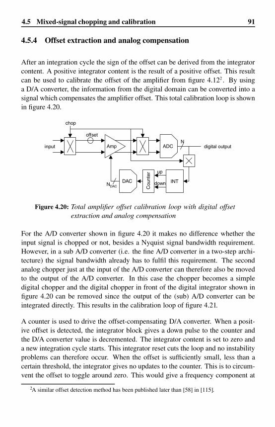
91
4.5.4 Offset extraction and analog compensation
After an integration cycle the sign of the offset can be derived from the integratorcontent. A positive integrator content is the result of a positive offset. This resultcan be used to calibrate the offset of the amplifier from figure 4.122 . By usinga D/A converter, the information from the digital domain can be converted into asignal which compensates the amplifier offset. This total calibration loop is shownin figure 4.20.
chop
Amp ADCN
offset
INTDAC
Cou
nter
up
downNDAC
input digital output
For the A/D converter shown in figure 4.20 it makes no difference whether theinput signal is chopped or not, besides a Nyquist signal bandwidth requirement.However, in a sub A/D converter (i.e. the fine A/D converter in a two-step archi-tecture) the signal bandwidth already has to fulfil this requirement. The secondanalog chopper just at the input of the A/D converter can therefore also be movedto the output of the A/D converter. In this case the chopper becomes a simpledigital chopper and the digital chopper in front of the digital integrator shown infigure 4.20 can be removed since the output of the (sub) A/D converter can be
A counter is used to drive the offset-compensating D/A converter. When a posit-ive offset is detected, the integrator block gives a down pulse to the counter andthe D/A converter value is decremented. The integrator content is set to zero anda new integration cycle starts. This integrator reset cuts the loop and no instabilityproblems can therefore occur. When the offset is sufficiently small, less than acertain threshold, the integrator gives no updates to the counter. This is to circum-vent the offset to toggle around zero. This would give a frequency component at
2
4.5 Mixed-signal chopping and calibration
extraction and analog compensationFigure 4.20: Total amplifier offset calibration loop with digital offset
integrated directly. This results in the calibration loop of figure 4.21.
A similar offset detection method has been published later than [58] in [115].

92
chop
Amp ADCN
offset
INTDAC
Cou
nter
up
down
input digital output
NDAC
the integration cycle length. This threshold can be calculated by multiplying theminimum offset which has to be detected, for example LSB
4 , by the total numberof integrated samples. Figure 4.22 illustrates the operation of the calibration loop.
Integratorcontent
DACvalue
threshold
Amplifiererror
¼ LSB
t
t
t
Pseudo randomCycle length
Figure 4.22: Integrator and D/A converter signals of the calibration loop,together with the resulting error
The demands on the D/A converter are determined by the step size of the com-pensation. If the integrator is able to detect offsets of LSB
4 the step size (or res-olution) of the D/A converter should be less or equal to that value. The linearityof the offset compensation D/A converter is not critical since the D/A converter ispart of the regulation loop.
The described calibration loop enables offset calibration of the amplifier duringnormal operation. The amplifier and A/D converter are transparent for normalinput signals, while the offset of the amplifier is extracted in the digital domain.This enables the use of a filter or integrator with a large time constant, without the
choppingFigure 4.21: Total amplifier offset calibration loop with improved
Enhancement techniques for two-step A/D converters

93
drive a D/A converter to compensate for the amplifier offset.
4.5.5 Offset extraction in a dual-residue two-step converter
This calibration algorithm is not only applicable for the offset of a single ampli-fier in a single residue system. When dual-residue signal processing is used, asdescribed in section 4.3.2 and shown in figure 4.23a, the effect of offset on theresidue amplifiers on the transfer curve of the sub A/D converter is shown in fig-ure 4.23b. The offset of the residue amplifiers can be made small by design, butthis requires large input devices. To reduce the input capacitance of the residueamplifiers, the offsets of both amplifiers are calibrated.
Amp A
Amp B
subADC
offset B
offset AA
nA
B
nB offset A
offset B
input
subADC
output
inrangeoverrange
overrange
subADC
output
Figure 4.23: A dual-residue sub A/D converter system (a) and the effect ofthe residue amplifier offset on the transfer curve of the subA/D converter (b)
At the beginning of the range shown in figure 4.23b, the offset of amplifier A de-termines the deviation from the ideal curve, while at the end of the range the offsetof amplifier B determines the deviation from the ideal curve. The offsets of bothamplifier A and amplifier B, as shown in figure 4.24a, are split up into a commoncomponent and a differential component because they require a different detectionand calibration scheme, as will be explained later. The common offset componenthas equal values and equal signs for both amplifiers (figure 4.24b) and the differ-ential offset component has equal values but has opposite signs (figure 4.24c).
The offsets of both amplifiers can be written as a function of the common anddifferential offset components:
need for accurate or sensitive analog components. The extracted offset is used to
4.5 Mixed-signal chopping and calibration
(a) (b)

94
offset A
offset B
input
ADCoutput
offsetdiff A
offsetdiff B
input
offsetcomm A
offsetcomm B
input
=
+inrange
overrangeoverrange
inrangeoverrange
overrange
inrangeoverrange
overrange
Figure 4.24: The offsets of amplifiers A and B (a) split up into common (b)and differential (c) components
Voffset A = Voffsetcomm + Voffsetdiff
Voffset B = Voffsetcomm − Voffsetdiff
(4.14)
Equation 4.14 can be rewritten to calculate the common and the differential offsetcomponent from the amplifier offsets:
Voffsetcomm = Voffset A+Voffset B
2
Voffsetdiff = Voffset A−Voffset B
2
(4.15)
The effect of the common offset component is a DC shift of the transfer curveof the A/D converter. This does not reduce the non-linearity of the two-step A/Dconverter. In principle this offset does not have to be compensated for. However,
(a)
(b) (c)
Enhancement techniques for two-step A/D converters

95
since the common offset component causes a shift of the residue signal in the fineA/D converter range, it uses part of the over-range of the fine converter while thisis intended for the coarse A/D errors. When the common offset component isreduced as well, the total fine A/D converter over-range can be used for the coarseA/D converter errors. This allows the power of the coarse A/D converter to bereduced to the minimum. The differential offset component, however, directlyreduces the non-linearity of the two-step A/D converter. Both the common anddifferential offsets therefore need to be calibrated.
For the sake of simplicity, the offset detection without chopping of the residueamplifier inputs is considered first. In order to be able to extract the sign of thecommon or differential amplifier offset component, the effect of the respectiveoffset component should be a signal at DC. The sign of the offset can then bedetected by integration of the digital data (which is actually low-pass filtering).This is illustrated in figure 4.25.
Amp A
Amp B
subADC
offset B
offset AA
nA
B
nB
subADC
output
Processing IntegratorOffset sign
detector
Figure 4.25: Offset sign detection by integration of the digital output of adual residue amplifier conversion system
The additional processing in the digital signal path is to transform the signal suchthat a signal at DC appears when there is amplifier offset. It is clear that in thiscase a DC component in the input signal will interfere with the offset detection,although chopping of the residue amplifiers (described in section 4.5.1) removesthis restriction, as is explained later.
Common offset
First the common offset component from figure 4.24b is considered. In this casethe additional signal processing shown in figure 4.25 only puts the zero referencein the middle of the output range, as is shown in figure 4.26a.
4.5 Mixed-signal chopping and calibration

96
input
offsetcomm A
offsetcomm B
subADC
output
inrangeoverrange
overrange
f
sub ADCoutput [dB]
input signal
offset
Zero reference
0
Figure 4.26: Input of the integrator (a), with the zero reference in themiddle of the range and the spectrum (b) of the sub A/D con-verter output with only common offset
When the input signal of the residue amplifiers is a (randomly) varying signal(for example a sine with zero DC component), the signal varies at the x-axis offigure 4.26a. When both amplifiers of figure 4.25 have an equal offset, a DCcomponent appears in the output signal (figure 4.26b), which is caused by thisoffset. When the output signal of the sub ADC is applied to the integrator fromfigure 4.25, this DC component leads to a positive integrator content. This is ameasure for the sign of the offset and can be used in a calibration loop to removethe offset.
Differential offset
When the offsets of both residue amplifiers from figure 4.25 consist of only adifferential component the transfer curve of the sub A/D converter is shown infigure 4.24c. When the same processing as described above with common offsetis used, the input of the integrator as a function of the input signal is shown infigure 4.27a.
When in this case the input signal of the residue amplifiers is a (randomly) varyingsignal (for example a sine with zero DC component) similar to that describedabove, there is no offset component visible at DC. Figure 4.27b shows that theerror is only visible as a gain error, but this cannot be detected with the low-passfiltering of an integrator. To enable the detection of the differential offset as aDC component a larger part of the total A/D converter range (more sub-ranges) is
(a) (b)
Enhancement techniques for two-step A/D converters

97
input
offsetdiff A
offsetdiff B
inrangeoverrange
overrange
subADC
output
f
sub ADCoutput [dB]
input signal+offset
0
Figure 4.27: Input of the integrator (a), with the zero reference in themiddle of the range and the spectrum (b) of the sub A/D con-verter output with only differential offset
considered, as shown in figure 4.28a. The spectrum of the A/D converter outputis shown in figure 4.28b, when an example input signal without a DC componentis applied.
The differential offset is spread through the spectrum and indicated as
’
whitenoise’ in figure 4.28b. In reality, however, it shows up as discrete peaks, whichare input-signal-frequency-dependent. The additional digital processing detectswhether the output signal passes a threshold which lies in the middle of a sub-range. According to this detection, the proper value is subtracted from the digitalcode. The result is shown in figure 4.28c. This additional processing works ina similar way to the two-step processing, where the threshold lies at a subrangetransition. If the applied input signal contains no DC, the differential offset canstill not be detected by low-pass filtering, since there is no offset component atDC. By inverting the digital code in the odd
’
subranges’ as shown in figure 4.28d,part of the differential offset appears at DC in the spectrum (figure 4.28e). Dueto a differential offset the transfer curve is always above (or equal), or always be-low (or equal) to the ideal transfer curve (depending on the sign of the differentialoffset). This is illustrated in figure 4.28d. When any (random) signal without aDC component is applied to the A/D converter, which means that the input signalvaries over the x-axis of figure 4.28a, c and d, part of the differential offset appearsat DC. By low-pass filtering or digital integration, the sign of this offset can bedetected, in a similar way to the common offset.
4.5 Mixed-signal chopping and calibration
(a) (b)

98
input
offsetdiff A
offsetdiff B
totalADC
output
f
integratorinput [dB]
input signal
offsetdiff A
offsetdiff B
offsetdiff A
subtractedADC
output
integratorinput
inverted inverted
offset
f
total ADCoutput [dB]
input signal
offset
Figure 4.28: Output of the total A/D converter with 4 subranges, only dif-ferential offset on the residue amplifiers (a) and the spectrumof an example signal (b), subrange processing (c) and partialinverted integrator input (d) with the resulting spectrum (e)
Chopping
To be able to distinguish the offset error from the (DC) input signal, the inputs ofthe residue amplifiers are chopped, as explained in section 4.5. Since two amp-lifiers are chopped, there are four connection possibilities. With one un-choppedconnection, this results in three different chopping methods. This is illustrated infigure 4.29.
Chopping method 1 changes the polarity of the inputs of both amplifiers. Chop-ping method 2 also changes the polarity of the inputs and interchanges the inputsof amplifier A and amplifier B. The third chopping method leaves the polaritythe same and only interchanges the inputs of amplifier A and amplifier B. Thethree chopping methods deal with the common and differential offset components
(a)
(c)
(d)
(e)
(b)
Enhancement techniques for two-step A/D converters

99
Amp A
Amp B
chop
subADC
offset B
offset AA
nA
B
nB
AnA
BnB
nAA
nBB
AnA
BnB
nBB
nAA
AnA
BnB
BnB
AnA
31 2
chop
offsetextractor
input
subADC
output
Figure 4.29: Chopping of dual-residue amplifiers with three possibilitiesof chopping
in a different way. Only the first chopping method is considered here, since bothcommon and differential offsets can be detected using this chopping method. Theother two chopping methods can be used to detect only common or only differen-tial offset, but this is not discussed here.
When the inputs of the residue amplifiers are chopped (with chopping method 1)under the condition that only common offset is present at the residue amplifiers,the transfer curves of both chop states are shown in figure 4.30. The chop statenochop has the same transfer curve, as shown in figure 4.26a. The signal whichis applied to the input of the integrator shown in figure 4.25 comes from one ofthe transfer curves of figure 4.30, depending on the chop state.
The first effect of chopping is that the signal component is inverted for an equalsub A/D converter input signal. The second effect of chopping is that the offsetcomponent does not change sign for an equal sub A/D converter input signal. Thisis clear from figure 4.29 since the amplifier offset is added after chopping of thesignals. Suppose the example signal Vx shown in figure 4.30 is the input signalof the sub A/D converter in figure 4.25. The value on the nochop or chop1 curveis then applied to the integrator of figure 4.25, depending on the chop state. The
4.5 Mixed-signal chopping and calibration
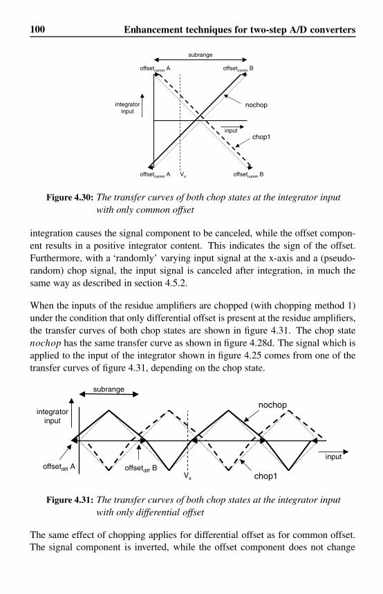
100
input
offsetcomm A
offsetcomm B
nochop
offsetcomm A
offsetcomm BVx
integratorinput
subrange
chop1
Figure 4.30: The transfer curves of both chop states at the integrator inputwith only common offset
integration causes the signal component to be canceled, while the offset compon-ent results in a positive integrator content. This indicates the sign of the offset.Furthermore, with a
’
randomly’ varying input signal at the x-axis and a (pseudo-random) chop signal, the input signal is canceled after integration, in much thesame way as described in section 4.5.2.
When the inputs of the residue amplifiers are chopped (with chopping method 1)under the condition that only differential offset is present at the residue amplifiers,the transfer curves of both chop states are shown in figure 4.31. The chop statenochop has the same transfer curve as shown in figure 4.28d. The signal which isapplied to the input of the integrator shown in figure 4.25 comes from one of thetransfer curves of figure 4.31, depending on the chop state.
inputoffsetdiff A
Vx
integratorinput
offsetdiff B
nochop
chop1
subrange
Figure 4.31: The transfer curves of both chop states at the integrator inputwith only differential offset
The same effect of chopping applies for differential offset as for common offset.The signal component is inverted, while the offset component does not change
Enhancement techniques for two-step A/D converters

101
sign. When an example signal is applied (Vx in figure 4.31), depending on thechop state, the value on the nochop or chop1 curve is applied to the integratorof figure 4.25. The integrator causes the signal component to be canceled, in asimilar way to that described above for a common offset component, while theoffset component causes the integrator content to be positive. This is caused bythe fact that the transfer curve with differential offset is always above (or equalto) the curve without offset in figure 4.31. The positive integrator content is ameasure for the sign of the offset. Also with a
’
randomly’ varying input signal atthe x-axis and a (pseudo-random) chop signal, the input signal is canceled due tointegration, in a similar way to that described in section 4.5.
The additional signal processing for both component extractions is different, withthe result that separate paths are used for the detection of the common and dif-ferential components. The complete system for extracting both the common anddifferential offset in the digital domain and compensating the extracted offset inthe analog domain is shown in figure 4.32.
subADC
Amp A
Common Offset
Extractor
Differential Offset
Extractor
Pseudo-Random
Generator
Σ
Σ++++
++++
++++
−−−−
Amp B
To Digital
Decoder
offset B
offset A
residueinput A
residueinput B
Figure 4.32: Complete digital offset extraction and analog compensationsystem
The effect of the difference of the compensation of the common offset and of thedifferential offset is illustrated by the signs at the summation points of the com-pensation D/A converter signals. A common offset results in an equal change ofboth compensation D/A converters, while a differential offset results in a changewith opposite sign.
4.5 Mixed-signal chopping and calibration
102
Because of the additional processing required to detect the differential offset, acommon offset component is averaged out in the differential offset extractor. Visaversa, the same holds for a differential offset component. A differential offsetcomponent is averaged out in the common offset extractor. The common anddifferential offset components can therefore be extracted simultaneously withoutinterfering with each other. A minor effect occurs when the input signal is a DCsignal or an input signal with a frequency which is lower than the cycle length ofthe calibration. In this case it is not possible to distinguish between a commonand differential offset component. To overcome this problem a detector is used tocheck if the input signal is distributed sufficiently over the whole subrange. In thedigital domain, the subrange is divided into 4 bins. The number of occurrenceswithin each bin is counted. When the number of occurrences in all of the 4 binswithin an integration period is above a certain threshold, the signal is then distrib-uted sufficiently. If this is not the case the outcome of the integration cycle is notused.
4.5.6 Conclusions
The mixed-signal chopping and calibration technique enables offset extraction inthe digital domain and compensation in the analog domain. The powerful sig-nal processing capability of the digital CMOS technology is used to make largetime constants, enabling highly accurate offset extraction. The required analogcircuitry is not critical in terms of accuracy and power. The calibration techniquedoes not require additional calibration time and operates under normal conver-sion conditions. The calibration can therefore be performed continuously withoutinterfering with the normal operation of the A/D converter.
Enhancement techniques for two-step A/D converters

Chapter 5
A 10-bit two-step ADC withanalog online calibration
5.1 Introduction
The scope of the experiment [28] described in this chapter is to verify the dual-residue signal processing [3] from section 4.3.2 in combination with analog offsetcalibration [106] in the two-step architecture [26] (section 3.4). In the previouschapters the basic architectural choices that involve both the accuracy of the con-verter and the speed were discussed. The experiment described in this chaptershows an implementation based on the theory developed in the previous sections.The quantization of video signals is used as a vehicle. Application as an embeddedvideo converter requires that the specifications in table 5.1 are met.
Table 5.1 shows the general requirements for video conversion for baseband sig-nals. Cost requirements demand that the A/D converter is embedded in a digitalCMOS chip. The technology, supply and sample rate choices are therefore givenby the video architecture [116]. In video systems, the signal from the tuner isdown-converted in the IF section. Subsequently, the CVBS signal is split intochrominance and luminance signals (YUV). The choice is between a single high-performance A/D converter for CVBS, which is what is focused on in this experi-ment, or a triple A/D converter for YUV. In the A/D converter for CVBS discussedhere, the color signal is still at 4.433 MHz, which means that the A/D converterperformance at this frequency will determine the quality of the color performance.
103

104
Resolution 8 bit for YUV, 10 bit for CVBS
Supply
Effective bandwidth
Sample Rate
DNL
INL
Power dissipation
Area
Technology
Single supply acc. to architecture
3 MHz for YUV, 5.5 MHz for CVBS
13.5, 27, 54 MSample/s depending on DSP choice
Strict monotonical (< 0.7 LSB)
Up to 3 LSB tolerable
< 250 mW (for embedding as low as possible)
< 1 mm 2
Digital CMOS without options
Color carrier < 1o phase delay at 4.433 MHz
Table 5.1: Requirements for video conversion
The DNL is the most critical parameter for luminance. In scenes with low lumin-ance variation a large DNL will result in visible artifacts (
’
contouring’). In CVBSthis demand is more stringent as the dynamic range of the signal is larger. The dy-namic properties of the A/D converter also need to be sufficient for performanceat the color carrier frequency. INL errors translate into distortion at higher signalfrequencies, thereby deteriorating the color performance.
In order to enable embedding in larger processing chips, the power consumptionand the area must be as low as possible. The target of 250 mW was chosen, whichis a quarter of the maximum power dissipation in a low-cost IC-package.
The traditional two-step architecture requires an amplifier stage with an exact gainfactor. Using dual-residue signal processing, the gain requirements are limited tothe gain matching of two residue amplifiers. The offset on these residue amplifiersmakes a major contribution to the INL of the converter. Their offset is calibratedin order to reduce the input capacitance of these amplifiers. Due to this offsetcalibration, the total intrinsic capacitance can be reduced significantly, thereby re-ducing the power. This calibration is relatively simple since only two componentsneed to be calibrated. The performance improvements due to dual-residue signalprocessing with offset calibration result predominantly in better linearity metricssuch as DNL, INL and spurious-free dynamic range (SFDR).
The accuracy of the two-step converter depends on the subtracting D/A converteraccuracy, the coarse and fine quantizer accuracy and the summing accuracy, allof which are very much dependent on the actual circuit implementation. Theaccuracy of the implemented converter described in this chapter depends mainlyon the ladder resistor matching and the offset of just two residue signal amplifiers.
A 10-bit two-step ADC with analog online calibration
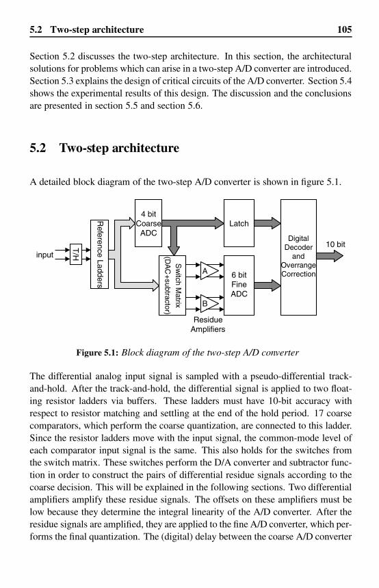
105
Section 5.2 discusses the two-step architecture. In this section, the architecturalsolutions for problems which can arise in a two-step A/D converter are introduced.Section 5.3 explains the design of critical circuits of the A/D converter. Section 5.4shows the experimental results of this design. The discussion and the conclusionsare presented in section 5.5 and section 5.6.
5.2
A detailed block diagram of the two-step A/D converter is shown in figure 5.1.
T/H
4 bitCoarseADC
Reference Ladders6 bitFineADC
DigitalDecoder
andOverrangeCorrection
Latch
Sw
itch Matrix
(DA
C+
subtractor)
ResidueAmplifiers
input10 bit
A
B
Figure 5.1: Block diagram of the two-step A/D converter
The differential analog input signal is sampled with a pseudo-differential track-and-hold. After the track-and-hold, the differential signal is applied to two float-ing resistor ladders via buffers. These ladders must have 10-bit accuracy withrespect to resistor matching and settling at the end of the hold period. 17 coarsecomparators, which perform the coarse quantization, are connected to this ladder.Since the resistor ladders move with the input signal, the common-mode level ofeach comparator input signal is the same. This also holds for the switches fromthe switch matrix. These switches perform the D/A converter and subtractor func-tion in order to construct the pairs of differential residue signals according to thecoarse decision. This will be explained in the following sections. Two differentialamplifiers amplify these residue signals. The offsets on these amplifiers must below because they determine the integral linearity of the A/D converter. After theresidue signals are amplified, they are applied to the fine A/D converter, which per-forms the final quantization. The (digital) delay between the coarse A/D converter
5.2 Two-step architecture
Two-step architecture

106
and the digital decoder is necessary because the coarse and fine quantizations donot take place at the same time. The digital decoder combines the outputs of thecoarse and fine quantizer and corrects the coarse code for over-range detected inthe fine quantizer.
The partitioning of coarse and fine bits is an important design parameter in thetwo-step architecture, as is shown in section 3.4. The input circuitry of both coarseand fine (flash) A/D converters only has to drive a reduced number of comparatorscompared to a full-flash A/D converter, resulting in a major capacitive load reduc-tion. The gain between coarse and fine A/D converters reduces this load evenfurther while also lowering the accuracy requirements of the fine comparators.This allows the two-step A/D converter to achieve a high sampling speed at lowpower consumption. This converter has 4 coarse bits, 6 fine bits and an amplifiergain of 10, which means that the accuracy required of the fine A/D converter isreduced by a factor of 10. A better value would be 5 coarse and 5 fine bits accord-ing to equation 3.18, but this A/D converter does not use a full bit over-range inthe fine A/D converter, which changes the optimization.
The two-step architecture is suitable for high-speed sampling but the achievementof high linearity presents extra challenges to the implementation. In the followingparagraphs the most important issues are analyzed and the solutions are presented.
5.2.1 Coarse quantizer accuracy
The coarse quantization determines in which subrange the input signal lies. Anerror in the coarse quantizer (due to comparator offset) results in residue signalswhich are out-of-range for the fine quantizer. From section 3.4 it follows that,without redundancy, the comparators of the coarse quantizer would need to havethe same accuracy of the total A/D converter (N bits). Suppose an A/D converterwith N = 10, 4 coarse bits and an input signal with an amplitude Vpp = 1.6 V.To achieve a yield of 99%, 4σ spread of the offset of the comparator input stageshas to be smaller than a quarter of an LSB (derived using equation 3.1):
4σVoffset,coarse <1
4· Vpp
2N⇒ σVoffset,coarse < 0.1mV (5.1)
Such low offsets can only be obtained with very large transistors, as describedin section 2.2.1, with a capacitive load in the ten pF range because the areas of
A 10-bit two-step ADC with analog online calibration

107
these transistors determine their matching [4]. This would have a negative effecton the sampling speed or power consumption of the A/D converter. To overcome
the coarse comparators (σVoffset,coarse) is dependent on the number of over-rangecomparators (#ORC) which are added to the fine quantizer:
4σVoffset,coarse < (1
4+ #ORC) · Vpp
2N(5.2)
Equation 5.2 shows that the offset required in the coarse quantizer is relaxed asmore over-range comparators are added to the fine quantizer. Because the additionof extra comparators to the fine quantizer will make a negative contribution to thespeed and power consumption, the number of over-range comparators must beoptimized for these parameters.
5.2.2 D/A converter and subtractor accuracy
When the coarse quantizer has decided in which subrange the input signal lies,the result is applied to the D/A converter which generates an analog signal pro-portional to the coarse decision. This signal is subtracted from the analog inputsignal, generating a residue signal that is applied to the fine quantizer. The ac-curacy of both the D/A converter and the subtractor is very important because itdetermines the quality of the residue signal and can therefore limit the perform-ance of the A/D converter.
In this design, the references for the coarse A/D converter and the D/A converterare the same [117]. In this case the reference used to select the proper subrangeand the reference which is subtracted from the input signal are equal. When thisis not the case, a gain error between input signal and D/A converter output [88]may lead to non-monotonicity or missing codes. Possible errors in the subtractorinclude offset and distortion. The first can cause the residue signal to be out-of-range for the fine quantizer, and the second distorts the residue signal, whichcauses distortion in the transfer curve of the total A/D converter. To overcomethese problems, the D/A converter and subtractor function are implemented asswitches connected to the moving reference ladders. This is illustrated as a singleresidue system in figure 5.2 [90].
5.2
in the fine quantizer, as described in section 3.4 [29]. In this case the accuracy of
Two-step architecture
the stringent offset requirement in the coarse quantizer, over-range is applied

108
input
residuesignalsfrom
T/H
voltage
inp
inn
SwitchMatrix
CoarseADC
a
b
c
d
ea+
b+
c+
d+
e+
a+
b+
c+
d+
e+
a
b
c
d
e
ReferenceLadders
residue signalsto residue amplifiers
Figure 5.2: Reference ladders, coarse A/D converter, D/A converter andsubtractor generating the residue signals
In order to generate the proper residue signals shown on the left in figure 5.2,the switches are set according to the coarse quantization. This means there areno components that contribute to offset or distortion present in the signal pathup to the residue amplifiers. The coarse quantizer reference, the D/A converterreference and the subtractor are laid out as one compact block.
5.2.3 Coarse and fine A/D converter references
After the coarse quantization, the residue-signals have to be applied to the finequantizer. A major problem for high accuracy is that the range of the fine quant-izer has to fit perfectly in the selected subrange. If this is not the case, the finecodes will not be distributed equally over the subrange and missing codes canoccur. Figure 4.4 illustrates the case where the range of the fine quantizer is lar-ger than the coarse subrange. Dual residue signal processing (4.3.2) is used tocircumvent the occurrence of large code jumps at the subrange transitions. Thisis implemented by connecting both the top and the bottom of the fine referenceladder to the coarse reference ladder as shown in figure 5.3. In this figure theover-range has been left out for the sake of simplicity.
A 10-bit two-step ADC with analog online calibration
–
–
–
–
–
–
–
–
–
–

109
Digital
inn
inp
nres B
res A
Figure 5.3: Generation of four residue signals (ignoring over-range)
This means the range of the fine quantizer reference adapts itself automaticallyto the coarse subrange. It also means that small differences between the resistorvalues of the coarse reference ladder will not lead to missing codes. Another ad-vantage is achieved by switching in such a way that the same amplifiers, buffersand fine comparators are used when the change is made from one subrange intothe adjacent subrange (section 4.3.2) [91]. In this case one side of the fine ref-erence ladder remains connected to the coarse reference ladder while the otherside changes its tapping point, as shown in figure 5.3. The effect of this improvedswitching on the overall transfer curve of the A/D converter is shown in figure 5.4.
Continuity and monotonicity of the converter are guaranteed, even with residueamplifier offset, due to this improved switching.
5.2.4 Amplifier gain and offset accuracy
The two pairs of differential residue signals, which have been generated by switch-ing from the coarse reference ladder, are amplified before they are applied to thefine quantizer. This reduces the required accuracy of the fine quantizer. After again factor of 10, the LSB size is enlarged from 1.5 mV to 15 mV. This allows thesize of the input transistors of the fine comparators to be reduced and therefore thespeed to be increased or the power to be reduced. Because the 4 residue-signalsconsist of 2 differential signals, 2 differential amplifiers are used. The offsets ofthese amplifiers are important since they make a major contribution to the integral
5.2 Two-step architecture
offset A
nres A
res B
offset B
Amplifier A
Amplifier B

110
offset A
offset B
offset A
offset B
offset A
input
ADCoutput
subrange (i)subrange (i-1)subrange (i-2) subrange (i+1)
Figure 5.4: The effect of residue amplifier offset with improved switchingon the overall transfer curve (ignoring over-range)
tain subrange transition the offset of only one amplifier (for example amplifier A)is relevant. Near the next subrange transition, the integral linearity of the A/Dconverter is mainly determined by the offset of the other amplifier (amplifier B).Since only 2 amplifiers are used to amplify the residue signals, some additionalpower and area can be spent to reduce the offset on these amplifiers. This is doneby offset compensation, which is explained in the circuit design section.
Due to the offset compensation, the accuracy of the two-step A/D converter isdetermined mainly by the accuracy of the coarse reference ladders from which allsignals are taken.
5.3 Circuit design
The design of the critical circuits is described in this section. As the A/D con-verter is designed for embedded use, the circuits are designed differentially to beless sensitive to any disturbance coming from the substrate or supplies. First thetrack-and-hold circuit is described, followed by the combination of coarse A/Dconverter, D/A converter and subtractor, the reference ladder requirements, theoffset-compensated residue amplifiers and, finally, the fine A/D converter.
A 10-bit two-step ADC with analog online calibration
linearity of the A/D converter. Figure 5.4 shows that in the vicinity of a cer-

111
5.3.1 Track-and-hold circuit
The pseudo-differential track-and-hold circuit performs the sampling of the ana-log input signal at the input of the A/D converter. A single-ended channel is shownin figure 5.5.
input output
Φ Φvdd
vss
Chold
Figure 5.5: Track-and-hold (single channel)
The input signal is 0.8 V peak-to-peak single-ended, at a common mode level of1.0 V. The low DC level requires the use of NMOS switches that have sufficientlylow on-resistance. In order to prevent the overall SNR of the A/D converter frombeing affected by the thermal noise (equation 2.8), a sampling capacitor of 500 fFis used. The track-and-hold uses only one quarter of the total sampling period fortracking to maximize the settling time in the A/D converter. With a sample rateof 25 MSample/s, this equals 10 ns. The output signal of the track-and-hold hasto track a Nyquist-rate input signal to an error of less than 0.25 LSB of 10 bitswithin 10 ns. Therefore 8.3 τ equals 10 ns. This means that the analog bandwidthof the combination of buffer, switch and sample capacitor has to be more than135 MHz. Dummy transistors are added to compensate for the charge dump ofthe switch transistor [118].
5.3.2 Coarse A/D, D/A converter and subtractor
In order to generate the zero-crossings for the coarse A/D converter, the sampledsignal from the track-and-hold is applied to two floating resistor ladders. This isshown in figure 5.6.
The comparators connected to this coarse ladder determine the coarse bits. Theoutput signals of the comparators drive a digital XOR function, which selects the
5.3 Circuit design

112
fromT/H
inp
inn
SwitchMatrix
CoarseADC
a
b
c
d
ea+
b+
c+
d+
e+
ReferenceLadders
residue signalsto residue amplifiers
‘1’
‘0’
SwitchSelection
Figure 5.6: Schematic of the coarse A/D converter, D/A converter andsubtractor
proper switches connected to the coarse reference ladders to generate the properresidue signals for dual-residue signal processing. These XORs and switches arealso shown in figure 5.6. The switches consist of NMOS transistors. The gener-ation of the dual-residue signals is explained in figure 4.5 and figure 4.6, withoutover-range.
5.3.3 Coarse ladder requirements
The coarse resistor ladder determines the integral linearity of the A/D converterbecause the signals used for the fine conversion (i.e. the residue signals) are de-rived from this ladder. Poly-silicon with a sheet resistance of 140 � is used asresistive material. The capacitive load of the comparators and the switches con-nected to the ladder together with the required speed determine the total resistanceof the ladder. In poly resistors, the contact of metal-to-poly and the interface res-istance from low-ohmic to high-ohmic poly is sensitive to process spread [119].The connection of the ladder to the comparator inputs, as shown in figure 5.7, ismade in such a way as to ensure that there is no current flowing through metal-to-poly contacts and low- to high-ohmic poly, and that their resistance does notaffect the accuracy of the ladder.
A 10-bit two-step ADC with analog online calibration
–
–
–
–
–

113
Ladder Current
Comparatorinput
Comparatorinput
Comparatorinput
Comparatorinput
Figure 5.7: One single-ended coarse and D/A converter reference res-istor ladder without current through poly-to-metal contacts
5.3.4 Offset compensated residue amplifier
Before the residue signals are applied to the fine A/D converter they are ampli-fied. This is done by 2 differential amplifiers. Because the coarse A/D converterresolves 4 bits, the total input range is divided into 16 subranges. This allowsa residue gain of 16 to generate the same amplitude at the output of the residueamplifier compared to the total input signal range. However, one residue amplifierremains connected to the reference ladder during 2 subranges (figure 5.6), whichmeans that the gain factor has to be reduced to 8. In this design the gain factoris 10 because the distortion requirements after the amplifier are less stringent thanat the input of the A/D converter. Since the offsets of the residue amplifiers makea major contribution to the linearity of the A/D converter, they have to be min-imized. An online analog offset calibration [106] is implemented to reduce thecapacitive load of the input stages of the residue amplifiers. Since the amplifi-ers cannot be used during calibration, the compensation is performed during thecoarse quantization because then the amplifiers are not active in the signal path.
Both residue amplifier A and amplifier B consist of the amplifier shown in fig-ure 5.8, which is based on a degenerated differential pair with gain boosting toincrease the linearity [120]. When the switches connected to 1 are closed (1
is high), the amplifier is in amplification mode and its input signal and offset areamplified. During calibration, the amplifier is disconnected from the switch unitand the input of the amplifier is short-circuited (1 is low). During this periodonly the offset appears amplified at the output. Switch 2 is then closed and theamplifier enters negative feedback mode. This means that the amplifier forces itsinput signal, and also the output of the amplifier, to be equal to the offset divided
5.3 Circut design

114
inp(from switch unit)
inn(from switch unit)
outn(to Fine ADC)
outp(to Fine ADC)
vdd
vss
Φ1 Φ1
Φ2 Φ2
Φ1
Cs Cs
Φ2
Φ1
out
Figure 5.8: One of the two residue amplifiers with offset calibration
by the gain of the loop. The initial offset is reduced by the loop-gain of 10. Thismeans that the area and therefore input capacitance of the input transistors can bereduced by a factor of 100 (equation 2.6), thereby reducing the capacitive loadfor the reference ladders. To have a stable feedback loop, the pole formed bythe compensation amplifier has to be at a low frequency. The dominant pole ofthe feedback loop is determined by the storing capacitor Cs and the on-resistanceof the switch 2. The bandwidth of the offset compensation loop is small butbecause only static offsets have to be compensated this is not limiting.
5.3.5 Fine A/D converter
The conversion is completed in the fine A/D converter. OPAMP buffers apply theamplified residue signals to 2 resistor ladders to generate the zero-crossings byinterpolation for the fine conversion. Until now only the circuits without over-range were considered. Increasing the number of over-range levels reduces thetotal capacitance of the coarse A/D converter, but increases the capacitance of thefine A/D converter. The optimum value is found when the fine A/D convertergenerates an additional bit, as is discussed in section 3.4. In order to increase
A 10-bit two-step ADC with analog online calibration

115
the fine A/D converter by an additional bit, half an additional range is required ateach side of the in- range part. The over-range zero-crossings of the fine converterare generated by placing resistors in the feedback-loop of the OPAMP buffers.Because this additional range is inside the feedback path of the OPAMP, as isshown in figure 5.9, this has a negative effect on the stability of this OPAMP.The OPAMP can be made stable with a large amount of over-range but this doesinvolve excessive power. A better option when this effect is taken into accountis to add 10 comparators over-range at each side in the fine A/D converter. Theincrease in allowed offset in the coarse A/D converter can be calculated usingequation 5.2:
σ(Voffset,coarse,#ORC=10
)σ
(Voffset,coarse,#ORC=0
) =14 + 10
14
= 41 (5.3)
This results in a reduction in capacitive load in the coarse A/D converter of 412.The total fine A/D converter is shown in figure 5.9.
output ResidueAmplfier A
output ResidueAmplfier B
over-range taps
OPAMP OPAMP
OPAMP OPAMPPreAmps PreAmps Comparators
over-range taps
in-range taps
Figure 5.9: Fine ADC with over-range generation and interpolation
5.3 Circuit design
16 + 6 32 + 12 64 + 20

116
The 16 in-range and 6 over-range pre-amplifiers amplify the resistor ladder tapsignals by a factor of 3. The outputs of these amplifiers are connected to 32 in-range and 12 over-range pre-amplifiers. Taking the outputs of adjacent pre-ampli-fiers generates the additional zero-crossings [15] (3.2.2). After these pre-amplifiers,32 in-range and 12 over-range zero-crossings are generated. Again, by interpola-tion, 64 in-range and 20 over-range zero-crossings are detected by comparators toconvert the analog zero-crossings to digital signals. The 64 comparators comparethe in-range zero-crossings, while the extra 20 comparators compare the over-range zero-crossings of the fine A/D converter. Using this interpolation method,only a total of 22 pre-amplifiers are connected to the fine resistor ladder, limitingthe capacitive load and thus increasing speed or reducing power. Due to the gainof the pre-amplifiers in front of the comparators, the effect of the comparator off-set is also reduced, which has a positive effect on the DNL of the A/D converter.
5.3.6 Timing
The timing in the two-step A/D converter is determined by the required settlingtimes of the various blocks. The timing is shown in figure 5.10.
Track Hold
Coarse Decision Fine Decision
Short Amplifier input Residue Amplification
Offset Compensation
T/H output
timeSample Period
V
Figure 5.10: Timing of the A/D converter
During the track time, the analog input signal is applied to the A/D converter. Thetrack-and-hold samples this signal and holds it for the remaining part of the sampleperiod. After the coarse quantizer has settled, the coarse decision can take place.Using this result, the proper switches are set in the switch unit. This also needssome time to settle. Next, the residue amplifiers are switched on and amplify theresidue signals. These signals are applied to the fine quantizer where, after some
A 10-bit two-step ADC with analog online calibration
Input Signal

117
settling time, the final fine decision is taken. After this decision, the track-and-hold can track a new sample and the amplifier inputs are shorted. The amplifieroffset-compensation takes place after the output of the amplifier has settled tozero. This cycle is repeated every 40 ns (25 MSample/s).
5.4 Experimental results
All the measurements in this book have been done using the test setup shown infigure 5.11.
The supply sources are HP3631A and the reference current sources are Keithley224. The clock reference for signal generation, A/D converter clock generationand data capturing are generated by the Agilent 81134A (formerly Agilent 8133A).The signal generator is an arbitrary waveform generator (Tektronix AWG2021).
5.4 Experimental results
converters designed in this bookFigure 5.11: Photograph of the test setup for characterizing the A/D

118
The output data from the A/D converter is captured by a logic analyzer (Agilent1682AD). All the equipment is set by a Labview program, which also does thesignal analysis. A screenshot of the Labview program is shown in figure 5.12.
Figure 5.12: Screenshot of the Labview program for equipment settingsand signal analysis
The screenshot of figure 5.12 is used for the 16-bit A/D converter from chapter 7.
The two-step A/D converter has been implemented in a 0.35µm standard digitalCMOS technology. No extra options, such as double-poly capacitors, have beenused. The A/D converter operates with a supply voltage of 3.3 V and has a powerconsumption of 195 mW. The power consumption of each block separately is notavailable. The area of the A/D converter is 0.66 mm2 including the track-and-holdand clock generation circuit. A die photograph is shown in figure 5.13.
The track-and-hold, reference ladders and coarse comparators are located at thetop left-hand side. To the right side of these are the offset-compensated amplifiersand fine ladder buffers. The fine A/D converter with 64 + 20 comparators issituated at the bottom of the block. The digital decoder is located at the top right-hand side.
A 10-bit two-step ADC with analog online calibration
A separate analysis program exists for the dynamic and static measurements.Each A/D converter has it own equipment configuration and Labview program.

119
Chip Micrograph
T/H
Reference ladders
Coarse ADC
Switch Unit
Residue Amplifiers
Fine Ladder Buffers
Fine ADC
Digital
Decoding
Figure 5.13: Die photograph of the 10-bit A/D converter
2
1
0
1
2
0 1024
2
1
0
1
2
0 1024Output Code
DN
L [L
SB
]IN
L [L
SB
]
Figure 5.14: Measured DNL and INL (1 MHz, 25 MSample/s)
Figure 5.14 shows the DNL and INL measurement obtained at a sample rate of25 MSample/s and an input signal frequency of 1 MHz. The DNL and INL are0.7 LSB and 0.9 LSB respectively. Figure 5.15 shows the output spectrum of theA/D converter with a 1 MHz full-scale input signal, sampled at 25 MSample/s.This figure shows that, due to the offset compensation and the improved switch-ing, the spurious components are below 72 dB. Figure 5.16 shows measurements
–
–
–
–
5.4 Experimental results
Output Code

120
120
100
80
60
40
20
0
0 2,5 5 7,5 10 12,5
f [MHz]
FFT [dB]
72 dB
Figure 5.15: Measured output spectrum (1 MHz, 25 MSample/s)
7.5
8
8.5
9
9.5
10
EN
OB
50
55
60
65
70
75
0 2.5 5 7.5 10 12.5 15
f [MHz]
SF
DR
, -T
HD
, SN
R [d
B]
SFDR
SNR
-THD
in
of SFDR, total harmonic distortion (THD) and SNR as a function of the inputsignal frequency with a sample rate of 25 MSample/s. The performance slightlydegrades for higher signal frequencies. The ENOB is 9.0 at DC and more than8.5 for input signals up to 12 MHz, resulting in an effective resolution band-width (ERWB) of 12 MHz. The FoM calculated with equation 3.35 is equal to14,21 pJ/conv. When normalized to the input voltage amplitude equation 3.37, itequals: 36,39 pJV2/conv.
A 10-bit two-step ADC with analog online calibration
–
–
signal frequency (25 MSample/s)Figure 5.16: ENOB, SFDR, -THD and SNR as a function of the input
–
–
–
–

121
Resolution 10 bit
Supply
Input range
ERWB
ENOB
SNR
THD
SFDR
Technology
3.3 V
1.6 Vpp
12 MHz
9
58 dB
62 dB
72 dB
Sample rate 25 Msample/s
INL
DNL
Power
0.9 LSB
0.7 LSB
195 mW
Area 0.66 mm2
Table 5.2: Overview of the performance measured
5.5 Discussion
No special care has been taken in creating an exact residue amplifier gain factorand the offsets of the residue amplifiers have been reduced by a factor of 10, whichis sufficient to achieve a DNL and INL of 0.7 LSB and 0.9 LSB respectively.The DNL and INL before calibration is not available since in this realization thecalibration cannot be switched off. The DNL is most probably limited to 0.7 LSBby the offsets of the comparators and pre-amps in the fine A/D converter. In orderto improve this larger input devices would be required for the comparators, whichwould degrade the speed or increase the power. A small residual offset componentcan be distinguished in the INL measurements, as an 8 times repeating pattern, butthe INL is still below 0.9 LSB. A larger offset compensation loop gain would berequired to improve this. The SFDR is 72 dB for a 1 MHz signal. The SFDR andTHD are a consequence of the INL curve.
The limitations of the proposed technique are identified as insufficient calibrationloop gain and required calibration time. The solving of these limitations in theanalog calibration circuits always results in a trade-off between speed and accur-acy versus power. A fundamental problem in this technique is that the DC error
5.5 Discussion
Single poly 0.35 µm CMOS
–

122
in the amplifiers is corrected every sample clock cycle. This imposes unnecessarybandwidth requirements on the calibration loop and requires an additional frac-tion of each conversion cycle. In this implementation this additional time fractionresults in a reduction of a factor of two in sampling speed. This can be seen infigure 5.10, where half of the sampling period is used for calibration of the residueamplifiers. This increases the achievable FoMVpp by a factor of 2. Since in thisexperiment the A/D converter has not been optimized for power, the FoMVpp islarger than expected from figure 3.33. The power could be reduced by optimizingin the second stage, for example, using a pipe-line 6-bit converter. The FoMVpp
can be further improved by reducing the power of the several building blocks inthe converter and using more advanced technology.
If the measurement results are compared with the video requirements as definedin section 5.1, this A/D converter is shown to meet the specifications. The A/Dconverter achieves over 9 ENOB at DC and has a SFDR of over 72 dB at a samplerate of 25 MSample/s. The effective resolution bandwidth is close to the Nyquistfrequency of 12.5 MHz. The A/D converter is fabricated in a 0.35 µm standardCMOS technology without options; it measures 0.66 mm2 and consumes 195 mWat a supply voltage of 3.3 V.
5.6 Conclusions
The limitation of the present calibration implementation is the result of the com-bination of A/D conversion and offset cancellation in one clock cycle. The nextchapter will describe a realization which circumvents this trade-off.
A 10-bit two-step ADC with analog online calibration
combination with analog offset calibration have been verified experimentally.Compared with the benchmark values in chapter 3, the power consumption is stilltoo high, but the performance meets the requirements for CVBS video signalprocessing.
In the experiment shown in this chapter the dual-residue signal processing in

Chapter 6
A 12-bit two-step ADC withmixed-signal chopping andcalibration
6.1 Introduction
The previous chapter shows that the speed limitation of analog compensation be-comes significant when considering figure 5.10. Due to the additional calibrationtime required, the maximum speed is limited to twice the minimum achievablesettling time. The scope of the experiment described in this chapter is to verifythe advantages of the dual-residue signal processing [3] from section 4.3.2 in com-bination with mixed-signal chopping and calibration (MSCC) from section 4.5 inthe two-step architecture [26] (section 3.4). A GSM base-station application hasbeen used as a test vehicle. In the early phase of GSM development, digitizationtook place on the demodulated baseband signal, see figure 6.1a. This position ofthe A/D converter in the signal chain relaxed the requirements on the A/D con-verter performance, however it imposed some stringent requirements on the sys-tem solution as a whole, e.g. channel selection had to be performed by setting thelocal oscillator. Moreover, this set-up required a full PCB for every channel. Ina second phase, the A/D converter moves to the IF domain, thereby moving largeparts of the filters into the digital domain. This A/D converter still serves onechannel, however more bandwidth and dynamic range are required, figure 6.1b.Ultimately the A/D converter will have to convert all channels in the GSM band
123

124
simultaneously. This will make it possible to move all channel-specific function-ality into the digital domain, and also to adapt relatively easily to new standardsthat occur in the same band (e.g. the EDGE protocol). Since there can be largesignals together with small signals, this requires a large A/D converter dynamicrange. It is obvious that excellent spurious free dynamic range performance isrequired and this directly translates into a very high specification on the overallaccuracy of the conversion function figure 6.1c.
ADCVGA DSP
ADCVGA DSP
ADC DSP
Figure 6.1: GSM base-station receiver with: baseband A/D conversion(a), single-channel IF A/D conversion (b) and multi-channelIF A/D conversion (c)
The trend in this application is to digitize a large number of channels with oneA/D converter. The intermediate step, as shown in figure 6.1b where each chan-nel in the IF-band is digitized with separate conversion chains, and a filter foreach channel will serve as the system driver in this chapter. With respect to onlybaseband conversion, this removes the requirement for a separate mixer for eachchannel. The dynamic range of the A/D converter is relaxed because of the useof a channel filter and an AGC. The requirements of an A/D converter in such asystem are shown in table 6.1.
Table 6.1 shows the general requirements for IF conversion for baseband signals.Cost requirements demand that the A/D conversion function is embedded in adigital CMOS chip. The GSM signal is down-converted to an IF frequency, res-ulting in a spectrum from 0 to 25 MHz in which the wanted channel has beenpre-filtered. However, large components from interferers and strong adjacent sig-nals can still be present. The 12-bit accuracy is sufficient together with the amountof channel filtering and the gain of the VGA. To be able to deal with the completeGSM band, the sample rate of the A/D converter has to be 50-60 MSample/s with
A 12-bit two-step ADC with mixed-signal chopping and calibration
(a)
(b)
(c)

125
Resolution 12 bit
Supply voltage
Effective bandwidth
Sample rate
Power dissipation
Area
Technology
Single supply acc. to architecture
25 MHz
> 50 Msample/s
< 400 mW
< 1 mm2
Digital CMOS without options
SNR
THD
SFDR
> 66 dB
> 70 dB
> 75 dB
an effective resolution bandwidth of 25 MHz. The SINAD of the GSM signalis only 9 dB, but in order to handle the large neighboring channels the SNR ofthe converter needs to be 66 dB. The spurious tones generated by large interfer-ing unwanted channels can disturb the reception of a small wanted channel. TheSFDR must therefore be below 75 dB. Distortion causes inter-modulation of largeunwanted signals, the resulting products of which can fall in the wanted channelband. Embedding of such a system requires low power and low area. The targetpower dissipation is chosen as 300 mW.
This chapter describes the realization [58] of a two-step A/D converter usinga mixed-signal chopping and calibration (MSCC) technique which reduces theresidue amplifier offset without requiring additional calibration time. The per-formance improvements due to MSCC are achieved predominantly for samplingspeed and INL and the corresponding linearity parameters such as THD andSFDR. Since the speed is improved by a factor of two with respect to the previ-ous chapter, the sample rate achieved is over 50 MSample/s. The more advancedtechnology is also beneficial for speed improvement. The offset reduction of theMSCC is more effective than the analog calibration from the previous chapter,which allows the accuracy to be increased to 12 bits. The MSCC operates on-line, which means that the A/D converter continues to operate during calibration.The calibration works continuously; gradually changing offsets are tracked. Theadditional analog circuitry for calibration is limited and is not demanding. Thedigital properties of the CMOS technology are exploited by using digital offsetextraction and storage. Large controlled time constants can be realized digitally,in a relatively small area.
6.1 Introduction
Table 6.1: Requirements for IF conversion

126
Section 6.2 of this chapter describes the two-step architecture. It shows howthe demands on the analog blocks in this design are minimized by architecturalchoices. Section 6.3 explains the mixed-signal and chopping and calibration al-gorithm, which is used to compensate the offset errors from the residue amplifiers.Some circuit designs are shown in Section 6.4. Section 6.5 and section 6.6 showthe experimental results and the discussion respectively. Finally, the conclusionsare presented in section 6.7.
6.2 Two-step architecture
A detailed diagram of the two-step A/D converter presented is shown in figure 6.2.
3X Interleaved S/H
input
VRB
VRT
5-bitCoarseADC
Ref
eren
ce
Ladd
er
ResAmps
8-bitFineADC
12 BITDigital
Decoderand
OverrangeCorrection
Switch
Matrix
Latch
B
A
Figure 6.2: Block diagram of the two-step A/D converter
The differential input signal is sampled with three interleaved sample-and-holdcircuits. The acquired analog signal is applied to the coarse A/D converter, whichcompares the differential input signal with a static reference ladder [121]. Com-parison of the signal to a static reference ladder increases the allowable inputsignal swing by a factor of 2, compared with when the differential input signalis applied to 2 floating ladders, as described in chapter 5. The result from thecoarse quantization is stored in a latch, and is also applied to a switch matrix. Ac-cording to the coarse quantization, this switch matrix selects 4 reference signalsfrom the same ladder as used for the coarse quantization. This is explained insection 6.2.3. These selected reference signals are combined with the held inputsignal in 2 residue amplifiers. The residue amplifiers perform the residue genera-tion and provide a gain of 8 before the residue signals are applied to the 8-bit fine
A 12-bit two-step ADC with mixed-signal chopping and calibration

127
A/D converter, which is explained in section 6.2.4. The accuracy requirements ofthe fine A/D converter are relaxed by providing gain to the residue signals. Sincethere are no error-contributing components up to this point in the signal path, ex-cept for the sample-and-hold and the static ladder, the offset generated in theseamplifiers is the main accuracy-limiting component in the A/D converter.
The optimum distribution of the coarse and fine bits found in section 3.4 suggestsa 6-bit coarse A/D converter, although an increase in the number of coarse bits
would cause the load of the reference ladder to increase. Decreasing the numberof coarse bits increases the accuracy requirements of the fine A/D converter, sinceit has to generate 9 bits instead of 8. The distribution for this A/D converter is setat a 5-bit coarse and an 8-bit fine A/D converter.
Since the fine A/D converter has half a subrange over-range available on both sidesof a subrange, the accuracy of the coarse A/D converter only has to be at half anLSB of its resolution, which equals 6-bit accuracy. The 8 bits of the fine A/Dconverter can be generated with sufficient accuracy without using compensationby using a folding and interpolating A/D converter. In the following paragraphsbuilding blocks are discussed in more detail.
6.2.1 Interleaved sample-and-hold
The use of interleaved sample-and-holds together with a static reference ladderenables pipe-lining in the A/D converter. The total sample-and-hold consists of3 identical interleaved [122] sample-and-hold circuits, as shown in figure 6.3.
The sample-and-holds all have the same input signals, while the clock signals areinterleaved in time. The clock signals are
’
one-high out of three’. This meansthat each sample-and-hold samples during one clock period, and holds during twoclock periods. Each step in the A/D converter has a full sample period settlingtime available, while settling to full 12-bit accuracy is only necessary at the inputof the residue amplifiers. This interleaving timing scheme enables high-speedsampling, since three actions (sampling, coarse and fine decision) can take placesimultaneously on different analog samples. This interleaving is also shown infigure 6.3. If sample-and-hold 1 (S/H1) is tracking the analog input signal (n),then S/H3 is carrying out the coarse quantization of the previous sample (n − 1),and S/H2 is performing the final quantization of two samples earlier (n − 2). The
6.2 Two-step architecture
but would also increase the number of switches for the fine reference selection. Thiswould not only increase the load of the coarse A/D converter by a factor of 8,
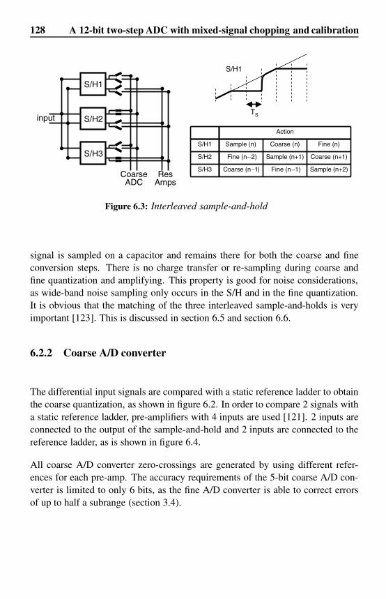
128
S/H1
S/H2
S/H3
CoarseADC
ResAmps
input
S/H1
S/H2
S/H3
Sample (n)
Fine (n 2)
Coarse (n 1)
Coarse (n)
Sample (n+1)
Fine (n 1)
Fine (n)
Coarse (n+1)
Sample (n+2)
Action
S/H1
TS
Figure 6.3: Interleaved sample-and-hold
signal is sampled on a capacitor and remains there for both the coarse and fineconversion steps. There is no charge transfer or re-sampling during coarse andfine quantization and amplifying. This property is good for noise considerations,as wide-band noise sampling only occurs in the S/H and in the fine quantization.It is obvious that the matching of the three interleaved sample-and-holds is veryimportant [123]. This is discussed in section 6.5 and section 6.6.
6.2.2 Coarse A/D converter
The differential input signals are compared with a static reference ladder to obtainthe coarse quantization, as shown in figure 6.2. In order to compare 2 signals witha static reference ladder, pre-amplifiers with 4 inputs are used [121]. 2 inputs areconnected to the output of the sample-and-hold and 2 inputs are connected to thereference ladder, as is shown in figure 6.4.
All coarse A/D converter zero-crossings are generated by using different refer-ences for each pre-amp. The accuracy requirements of the 5-bit coarse A/D con-verter is limited to only 6 bits, as the fine A/D converter is able to correct errorsof up to half a subrange (section 3.4).
A 12-bit two-step ADC with mixed-signal chopping and calibration
−− −

129
inp refprefn
outpoutn
inn
Coarse level
Coarse level
Coarse level
Coarse level
inp
innV
refp
refn
outn
outp
Res. Amp. output
input
input
6.2.3 Switching and residue signal generation
The coarse decision generates a thermometer code and an XOR block is usedto generate a
’one high’ code from this thermometer code. The input range of
the A/D converter is divided into a number of sub-ranges (SUB). The amount ofsub-ranges is equal to the number of coarse levels. The
’
one high’ code selectsthe proper sub-range in which the input signal is located. To be able to generatethe proper (dual) residue signals for the fine quantization, the switch unit selects4 references from the static reference ladder according to the
’one high’ code.
The 2 closest references to the differential sample-and-hold output signal and the
In order to be able to use the improved switching approach as described in sec-tion 4.3.2 [91], refB and nrefB remain connected to the reference ladder whenswitching from subrange SUB(n) to SUB(n + 1). The selected references refAand nrefA together with the differential output signal of the sample-and-hold areapplied to residue amplifier A, while refB and nrefB together with the differentialoutput signal of the sample-and-hold are applied to residue amplifier B. Theseamplifiers (which will be explained in the next section) combine their input signalaccording to the following equation:
resA = inp − refAnresA = inn − nrefAnresB = inp − refBresB = inn − nrefB
(6.1)
6.2 Two-step architecture
different referencesFigure 6.4: Pre-amplifier with 4 inputs to generate zero-crossings at
subrange SUB(n) and subrange SUB(n + 1).2 second closest references are selected. This is illustrated in figure 6.5a for

130
Coarse level
Coarse level
Coarse level
Coarse level
Coarse level
Coarse level
inp
inn
nrefA
refA
refB
nrefB
SUB(n) SUB(n+1)
resA
nresA
resB
nresB
nrefA
refA
Reference ladder
V
Res. Amp.output
input
input
In equation 6.1, resA and nresA are the differential output signals of residue amp-lifier A, while resB and nresB are the differential output signals of residue ampli-fier B. The result of this is shown in figure 6.5b. Both pairs of residue signals areapplied, via buffers, to 2 floating resistor ladders of the fine A/D converter whichgenerate the required fine quantization levels, as will be explained in section 6.4.The fine A/D converter range of SUB(n) begins at the zero-crossing of the sig-nals resA and nresA and ends at the zero-crossing of the signals resB and nresB.The subrange transition from SUB(n) to SUB(n + 1), as shown in figure 6.5, isdetermined by the coarse quantization and in the case of figure 6.5 is ideal. How-ever, when the coarse quantization is not accurate, the subrange transition is atanother position. This is illustrated in figure 6.6a.
Because the fine A/D converter range is from the zero-crossings of resA and nresAto the zero-crossing of resB and nresB, there are no quantization levels at the rightof the zero-crossing of resB and nresB, indicated by the circle in figure 6.6b,causing the fine A/D converter to clip. After the subrange transition from SUB(n)
to SUB(n + 1), the fine A/D converter range does not start at the zero-crossing
A 12-bit two-step ADC with mixed-signal chopping and calibration
(a)
(b)
amplifier outputs without over-range (b)Figure 6.5: Signal switching without over-range (a) and the residue

131
Coarse level
Coarse level
Coarse level
Coarse level
Coarse level
Coarse level
inp
inn
nrefA
refA
refB
nrefB
SUB(n) SUB(n+1)
resA
nresA
resB
nresB
nrefA
refA
Reference ladder
V
Res. Amp.output
input
Coarse error
Out of fine converter range
input
Figure 6.6: Signal switching with coarse A/D converter error, withoutover-range (a) and the corresponding residue amplifier out-puts (b)
quantization levels left from the subrange transition are therefore not used. Thiscauses missing codes in the transfer curve of the total A/D converter similar tofigure 3.18 [29]. To circumvent the occurrence of missing codes, over-range isapplied in the fine A/D converter (section 3.4). The fine A/D converter does notuse the same references as are used by the coarse decision to generate this over-range (as was shown in figure 6.5), but connects to other reference taps in orderto double the fine A/D converter range. This is shown in figure 6.7a.
In figure 6.7b the corresponding output signals of the residue amplifiers show thatin this case the fine A/D converter input-referred range is from A to B. Thiscreates an overlap in the subrange transition (see also figure 3.19) from C to B,which means that coarse errors can be corrected as long as they are between C
and B. This coarse error correction (figure 3.20) is performed by the over-rangecorrection of the digital decoder shown in figure 6.2.
6.2 Two-step architecture
(a)
(b)
of resB and nresB, but has skipped part of the fine A/D converter range. The

132
Coarse level
Coarse level
Coarse level
Coarse level
Coarse level
Coarse level
inp
inn
nrefA
refA
refB
nrefB
SUB(n) SUB(n+1)
resA
nresA
resB
nresB
nrefA
refA
Reference ladder
V
Res. Amp.output
input
nrefB
refB
BA C
input
Figure 6.7: Signal switching with over-range (a) and the correspondingresidue amplifier outputs with over-range (b)
range by inserting resistors in the feedback part of the fine resistor ladder buffers.
6.2.4 Residue amplifiers
The residue amplifiers are shown in figure 6.8.
The residue amplifiers have two functions. They act as subtractors to combinethe output signals from the sample-and-hold and the selected reference signalsto generate the residue signals which are applied to the fine A/D converter. Thesubtraction is done by two differential pairs similar to those in figure 6.4, whereinp and inn are the output signals of the sample-and-hold and refp and refn are theselected references refA and nrefA for residue amplifier A and refB and nrefB forresidue amplifier B, as described in the previous section. Their second functionis to amplify the residue signals. This reduces the accuracy (noise and matching)requirements of all circuits after this amplifier by the gain factor. Because of the
A 12-bit two-step ADC with mixed-signal chopping and calibration
Generation of the over-range part of the fine A/D converter by choosing the properreferences overcomes the limitation described in chapter 5 of generating the over-
(a)
(b)

133
refA ResAmp AnrefA
refBnrefB
inpinn
resA
nresA
resB
nresBRes
Amp B
from S/H
from Switch Unit
to Fine A/D converter
Figure 6.8: The two dual-residue amplifiers
use of dual-residue signal switching (section 4.3.2), the absolute gain requirementof the residue amplifiers is not important because this scales both the amplifiedresidue signals and fine A/D converter range. The matching between both residueamplifiers is more important, but this is dependent on poly-resistor matching, aswill be explained in the next section. The offsets generated in the residue amplifiermainly determine the linearity of the A/D converter. The next section describes amixed-signal chopping and calibration algorithm to calibrate this offset.
6.3 Mixed-signal chopping and calibration
The dominant error-contributing components in the signal path before gain is ap-plied are the sample-and-hold, the reference ladder, the switches in the switchunit, and the offset on the residue amplifiers. Sufficient power is expended in thesample-and-hold to meet the noise and linearity requirements. Matching of thereference ladder resistors is sufficient for 12 bits. The switches are just simpleNMOS switches, designed to have a sufficiently low on-resistance. This providessufficient bandwidth for 12-bit settling of the reference signals on the residueamplifiers. The offset on the residue amplifiers is now the only accuracy-limitingcomponent. Reduction of the offset to better than 12-bit accuracy requires largedevices, which limits the speed of the converter. Mixed-signal chopping and cal-ibration (section 4.5) is applied to the residue amplifiers to allow the use of smalldevice sizes and maintain speed and offset accuracy in the residue amplifiers. Thiscalibration is performed on-line, which means that no additional calibration timeis required and the converter is quantizing the input signal, while also carryingout the offset calibration. The digital processing capability of the CMOS tech-nology is used to extract the offset from the A/D converter output. Digital signalprocessing allows filters to be created with large time constants. Since offset is an
6.3 Mixed-signal chopping and calibration

134
analog property, a calibration D/A converter is used to compensate for the offseton the residue amplifiers.
6.3.1 Residue amplifier offset
Due to the improved switching (section 4.3.2) [91], offset on both amplifiers af-fects the transfer curve, as shown in figure 6.9. The offset of only one of bothamplifiers is shown at a subrange transition. This gives a deterministic, repeatedpattern in the INL curve of the A/D converter, and the offsets can therefore bemeasured in the digital domain by observing the regular digital signal at the out-put of the A/D converter.
offset B
offset A
offset B
offset B
to Digital Decoder
8 BitFineADC
SUB(n) SUB(n+1)SUB(n 1)SUB(n 2)
refA ResAmp AnrefA
refBnrefB
inpinn
ResAmp B
from S/H
from Switch Unit
offset A
offset A
ADC output
ideal output
output with offset
input
Figure 6.9: Transfer curve of A/D converter with residue amplifier offset
6.3.2 Chopping
To distinguish the offset of the residue amplifiers from the input signal of the A/Dconverter, chopping is applied to the inputs of both amplifiers (section 4.5). Therequired bandwidth in the amplifiers is not increased due to chopping because thechopping takes place at the same time as the subrange selection takes place. Thisis explained in section 4.5.
A 12-bit two-step ADC with mixed-signal chopping and calibration
− −

135
6.3.3 Digital extraction
Because in the case of two residue amplifiers the offset of both amplifiers is de-termined randomly, they can have any value. However, they can always be splitup into two components: a common component, which is an equal value for bothamplifiers, and a differential component, which is also equal but has the oppositesign (figure 4.24). A common offset component will only give a DC shift in thetransfer of the A/D converter, and therefore seems harmless at first sight. How-ever, such an error on the amplifiers will reduce the over-range capability in thefine A/D converter, which results in a smaller allowable offset in the coarse A/Dconverter. To extract both common and differential offset components the chop-ping method, as described in section 4.5.5, is applied. The total compensationloop is shown in figure 6.10.
8 BitFineADC
AmpA
Common Offset
Extractor
Differential Offset
Extractor
Pseudo-Random
Generator
Σ
Σ++++
++++
++++
AmpB
to Digital Decoder
12 Bit Digital
DecoderOutput
offset B
offset A
refAnrefA
refBnrefB
inp
innfrom S/H
from Switch Unit
Figure 6.10: Complete compensation loop with choppers, residue amplifi-ers, fine A/D converter and digital processing
Both residue amplifiers have a chopper at the input. The signal is quantized inthe 8-bit fine A/D converter after amplification by the residue amplifiers. In thedigital domain the data is chopped back to retrieve the original input signal and isapplied to the decoder to generate the 12-bit output of the A/D converter. This 12-bit output is applied to a common and a differential offset extractor. In this designnot only the fine A/D converter output (as described in section 4.5), but the total12-bit A/D converter output is applied to the digital offset extractor. This is notprincipally different. However, using only the fine A/D converter results in smal-ler required integration cycle lengths since the amplitude of the signal content issmaller (section 4.13). This signal is processed in order to retrieve the respective
6.3 Mixed-signal chopping and calibration
−

136
offsets at DC and by integration of the resulting signal the sign of both commonand differential offset are extracted (section 4.5.5). The resulting sign is used tochange the values of the digital signals which are applied to the offset compens-ation D/A converter located inside the residue amplifiers. The different effects ofthe common and the differential offset extractors can be seen at the ladders. Achange caused by the common offset extractor gives both D/A converter values astep of the same sign, while a change caused by the differential offset extractorgives a step of the opposite sign. These D/A converters close the compensationloop, thereby removing the offset in the residue amplifiers.
The calibration algorithm presented (section 4.5) does not need a dedicated testsignal and does not require a part of the conversion time. It works continuouslyand with every signal applied to the A/D converter. The major advantage of thismixed-signal chopping and calibration algorithm is that it extracts the errors fromcritical analog components in the digital domain, and compensates these errors inthe analog domain.
6.4 Circuit design
6.4.1 Interleaved sample-and-hold
The sample-and-hold used in this design consists of three identical sample-and-hold circuits. These sample-and-hold circuits are interleaved in time [122], asdescribed earlier. The sample-and-hold is shown in figure 6.11 [56, 33].
In the sample mode the single-stage folded cascode OPAMP is switched as a fol-lower. This means that the DC value of the ladder is present on one side of thesample capacitor, in addition to the offset of the OPAMP. When the sample-and-hold switches to
’
hold’ mode, the sampling capacitor, which now contains the sig-nal value and the offset of the OPAMP, is connected across the OPAMP. The offsetis then applied to the capacitor with the reverse sign, thereby compensating for thesampled offset. The sampled value is seen at the output, with sufficiently low off-set for 12-bit accuracy. The offset difference between the three sample-and-holdsis very critical for high performance as well as the dynamic matching [123]. Thelatter is discussed in section 6.5 and 6.6.
A 12-bit two-step ADC with mixed-signal chopping and calibration

137
inp
inn
inp
inn
outp
outn
outp
outn
OPAMP
OPAMP OPAMP
Φ
Φ
Φ
Φ
Φ
Φ
Chold
Chold
Chold
Chold
Chold
Chold
Figure 6.11: Sample-and-hold circuit, split up into the sample phase andthe hold phase, the OPAMP offset is canceled at the output
6.4.2 Coarse A/D converter
The coarse A/D converter has to compare the two differential signals with thestatic reference ladder. 32 comparators generate 5 bits in the coarse A/D con-verter. Pre-amplifiers with interpolation (section 3.2.2) [15] are used because alot of power would be required to drive the load of 32 comparators which have anaccuracy of 6 bits at 54 MSample/s. Part of the coarse A/D converter is shown infigure 6.12.
There are 9 pre-amplifiers at the input, each with 4 inputs, two of which are thereference signals to which the input signal is compared. When the input signalsequal their respective references, the output crosses zero. Interpolation is appliedbehind this first pre-amplifier stage; the additional zero-crossings are generatedby combining the output signals from adjacent pre-amplifiers (section 3.2.2) [15].Connected to these 9 four-input pre-amplifiers are 17 two-input pre-amplifiers, asshown in figure 6.12. Interpolation is applied again, and these amplifiers drive32 comparators. The gain in the pre-amplifiers reduces the required accuracy,and thereby reduces the power consumption of the comparators. The fine A/Dconverter can correct for half a subrange error in the coarse A/D converter. Thisequals 28 mV, since the input range of the A/D converter is 1.8 V peak-to-peak.
6.4 Circuit design
Sample phase: Φ = 1 Hold phase: Φ = 0

138
Ref
eren
ce la
dder
17Pre-amps
9Pre-amps
33Comparators
inp refprefn
outpoutn
inp inn
inn
from S/H
inprefprefninn
Figure 6.12: Coarse A/D converter
6.4.3 Residue amplifier with offset compensating
Offset CompensationCurrent DAC
inpref inn
nrefres
nres
VCASC
RdegRout RoutRdeg
to fineA/D converter
from digitaloffset extractor
Figure 6.13: Residue amplifier with compensation current D/A converter
Figure 6.13 shows one of the residue amplifiers from figure 6.8. This amplifier has4 inputs, which are needed to perform the subtraction of the input signal with theselected references from the reference ladder, to generate the residue signals. Theinput transistors are designed for a sufficiently low thermal noise contribution tothe signal path. The degeneration resistors Rdeg are added for sufficient linearity.The offset of this amplifier mainly determines the accuracy of the A/D converter.This offset is therefore calibrated by a current D/A converter. This D/A converterdrives a current through the output resistors of the amplifier, such that the remain-ing offset of the amplifier is sufficiently low. The digital offset extraction block
A 12-bit two-step ADC with mixed-signal chopping and calibration
current D/A converter

139
determines the digital code applied to the current D/A converter. Linearity of theD/A converter is not an issue since it is part of a feedback loop. The DNL ofthe D/A converter determines the resolution of the offset compensation. A 9-bitD/A converter was sufficient to compensate the largest possible offset to LSB
10 ofthe overall A/D converter. The absolute value of the gain of the amplifiers is notimportant, as is explained in section 4.3.2. The matching of the gain is determinedby the matching of poly resistors and is sufficient for 12-bit accuracy.
6.4.4 Folding-and-interpolating fine A/D converter
The 4 residue signals from the residue amplifiers are connected to 4 OPAMPsswitched as buffers, which apply their output signals to both the top and bottomof 2 moving ladders, as shown in figure 6.14.
64+
4 C
ompa
rato
rs
Sou
rce
follo
wer
s +
Inte
rpol
atio
n
32 ti
mes
Bel
l sha
pe g
ener
atio
n
17 P
re-a
mpl
ifier
s
9 P
re-a
mpl
ifier
s
resA
nresA
resB
nresB
8 bi
t dec
oder
Ia
Ia
to Digital Decoderfrom
Res Amps
Figure 6.14: Folding and interpolating fine A/D converter
The direction of the current flowing in these ladders is determined by the selec-ted subrange and by the chop state. Two buffers therefore have to sink the laddercurrent, and 2 buffers have to source the ladder current, depending on the sub-range and chop state. The current is reversed in a subrange transition or a chopstate change. This can give rise to a jump in the output signal of the buffers dueto the large change in current. This effect can be reduced by introducing a largequiescent current in the output stage of the buffers, but this requires high power
6.4 Circuit design

140
dissipation. The solution used here is to provide this switching current by usingadditional current sources, Ia shown in figure 6.14. They are connected at the topand bottom of both ladders to sink or source the ladder current. Now the buffersonly have to deliver the error current, which is much less than the DC currentthrough the ladders. The fine A/D converter shown in figure 6.14 has to provide8 bits because a flash A/D converter would require 256 comparators (section 3.2),which would give too much load to the fine ladders. A folding and interpolatingA/D converter is therefore used (section 3.3). The signal is folded 4 times, re-quiring 64 comparators. Most folding A/D converters use 8 or 16 times folding(section 3.3) [16, 19, 23], however 4 times folding was used since a 6-bit full-flashfine A/D converter from a previous design was expanded to 8 bits by only addingthis 4 times folding block. Pre-amplifiers with interpolation [15] are used to gen-erate the zero-crossings, as described in section 3.2.2, and used in the coarse A/Dconverter. Nine pre-amplifiers are connected to the ladder, followed by 17 pre-amplifiers. Connected to these pre-amplifiers are 33 folding amplifiers, whicheach generate a bell-shaped signal [21] by coupled differential pairs, as shown infigure 6.15.
inp1
inn1
inp2
inn2
inp3
inn3
inp4
inn4
out12 out23 out34 out45out01
from
Pre-amplifiers
Figure 6.15: Bell-shaped signal generation by coupled differential pairs
These bell-shaped signals are combined with source followers [124], the sourcesof which are connected together. This is illustrated in figure 6.16 by the signalout12 + out34, composed from combining out12 and out34.
This generates 8 signals with 4 times folding. Then 64 zero-crossings are
A 12-bit two-step ADC with mixed-signal chopping and calibration
A/D converter.zero-crossings. Four additional comparators generate the
’
coarse’ bits of the finegengerated by resistive interpolation. Sixty-four comparators digitize these 64

141
out01
out12
out23
out34
out45
input
out12+out34
voltage
Figure 6.16: Generation of the folding signal from combination of the
6.5 Experimental results
The A/D converter has been fabricated in a standard 0.25 µm CMOS technologywith one layer of poly silicon and five layers of metal. No additional options wereapplied (neither controlled capacitors nor thick gate oxide transistors). The supplyvoltage is 2.5 V. The area of the A/D converter is 1 mm2. The die photograph isshown in figure 6.17.
Digital
InterleavedSample-and -Hold
CoarseADC
FineADC
DAC
AmpAmp
DAC
Chold
Refere
nce ladde
r
Figure 6.17: Die photograph of the 12-bit two-step A/D converter
6.5 Experimental results
bell-shaped signals

142
the left-hand side. The reference ladder and the coarse A/D converter are shownin the middle, in addition to the two residue amplifiers with the respective com-pensation D/A converters. The 8-bit folding and interpolating A/D converter withthe buffers and ladders is on the right-hand side. The digital offset extractionblock can be seen at the bottom.
The power consumption of the A/D converter is 295 mW (without output buffers).The power is divided over the different blocks of the A/D converter, as shown infigure 6.18.
SHA
Coarse ADCRes. Amps
Fine ladder buffers
Fine ADC Digital
The major power-consuming blocks are the SHA and the fine A/D converter. Ascan be seen in figure 6.18, the power contribution of the residue amplifiers tothe total power consumption is limited because of the offset compensation. Thepower for the digital circuits is only a small part of the total A/D converter powerconsumption and includes the digital decoder with over-range correction and theMSCC.
200220240260280300320340360380
0 20 40 60 80 100 120 140 160
Update Cycle
DA
C v
alue
DAC A
DAC B
Start Calibration
Figure 6.19: Calibration of the residue amplifiers
A 12-bit two-step ADC with mixed-signal chopping and calibration
The three interleaved track-and-hold blocks with their sample capacitors are on
converterFigure 6.18: The relative power consumption of each block of the A/D

143
in the mid-range at the starting point. When the calibration starts the differentialoffset component is first calibrated for some time. Then the common offset com-ponent is calibrated for a few cycles. This alternating calibration of common anddifferential offset continues until the offsets of both residue amplifiers are belowLSB
10 . The calibration shown in figure 6.19 does not require any special calibrationinput signal, but operates with any regular or irregular signal applied to the A/Dconverter, as has been proven in section 4.5. The offset is not necessarily constantover time but can change due to temperature or supply changes. As a result, oncethe offset is reduced below the desired threshold, the calibration is not stopped butcontinuously monitors whether an offset appears again on the amplifiers, and if soit calibrates them.
3
2
1
0
1
2
3
0 1024 2048 3072 4096
3
2
1
0
1
2
3
0 1024 2048 3072 4096
6
4
2
0
2
4
6
0 1024 2048 3072 4096
INL
wit
ho
ut
calib
ratio
n [
LS
B]
6
4
2
0
2
4
6
0 1024 2048 3072 4096
INL
wit
h c
alib
ratio
n [
LS
B]
Output Code Output Code
Figure 6.20: Measured DNL and INL with fs = 54 MSample/s andfin = 1.0 MHz without calibration (a) and with calibration(b)
Figure 6.20 shows the DNL and INL with (a) and without (b) calibration. TheDNL is not improved with this algorithm, as it is already small due to the dual-residue signal switching (section 4.3.2). The upper peaks in INL shown in fig-ure 6.20a are a measure of the offset on amplifier B (figure 6.9); the lower peaksare a measure of the offset on amplifier A. The DNL and INL after calibrationof figure 6.20 could have been further improved by improving the pre-amp andcomparator offset in the fine A/D converter.
6.5 Experimental results
Figure 6.19 shows the calibration from start-up. Both D/A converter values are
−−−
−−−
−−−
−−−D
NL
wit
h c
alib
rati
on
[L
SB
]D
NL
wit
ho
ut
calib
rati
on
[L
SB
]
(a)
(b)

144
Figure 6.21: Measured spectrum (with calibration) withfs = 54 MSample/s and fin = 1.0 MHz
A measured spectrum is shown in figure 6.21. The measurement has been per-formed at 54 MSample/s and a signal frequency of 1.0 MHz. It can be seen thatthe harmonic performance is good due to the offset calibration of the residue amp-lifiers. All spurious components are below 75 dB.
Figure 6.22: Dynamic performance (with calibration) measured withfs = 54 MSample/s
The dynamic performance measured at 54 MSample/s in figure 6.22 shows goodTHD performance up to the Nyquist frequency of 70 dB. However, the overallperformance decreases due to spurious components at fs
3 ± fin, which are non-harmonic spurs. The SFDR does not therefore reduce the THD performance, butreduces the signal-to-noise and distortion (SINAD). The components come from afrequency-dependent mismatch in the three interleaved sample-and-holds, which
A 12-bit two-step ADC with mixed-signal chopping and calibration
−
0
10
20
30
40
50
60
70
80
0 10 20 30 40f [MHz]in
[dB
]
-THD
SFDR
SINAD
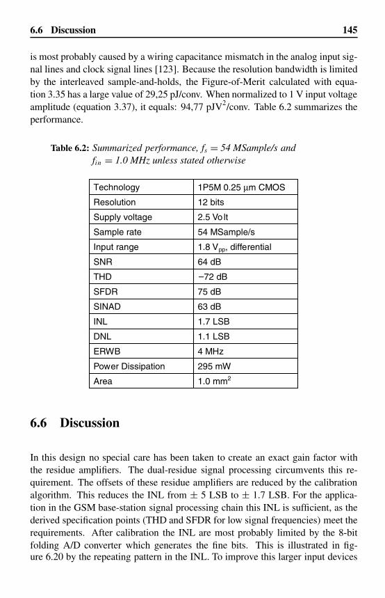
145
is most probably caused by a wiring capacitance mismatch in the analog input sig-nal lines and clock signal lines [123]. Because the resolution bandwidth is limitedby the interleaved sample-and-holds, the Figure-of-Merit calculated with equa-tion 3.35 has a large value of 29,25 pJ/conv. When normalized to 1 V input voltageamplitude (equation 3.37), it equals: 94,77 pJV2/conv. Table 6.2 summarizes theperformance.
Technology 1P5M 0.25 µm CMOS
Resolution 12 bits
Supply voltage 2.5 Vo lt
Sample rate 54 MSample/s
Input range 1.8 Vpp, differential
SNR 64 dB
THD 72 dB
SFDR 75 dB
INL 1.7 LSB
DNL 1.1 LSB
Power Dissipation 295 mW
Area 1.0 mm2
SINAD 63 dB
ERWB 4 MHz
6.6 Discussion
In this design no special care has been taken to create an exact gain factor withthe residue amplifiers. The dual-residue signal processing circumvents this re-quirement. The offsets of these residue amplifiers are reduced by the calibrationalgorithm. This reduces the INL from ± 5 LSB to ± 1.7 LSB. For the applica-tion in the GSM base-station signal processing chain this INL is sufficient, as thederived specification points (THD and SFDR for low signal frequencies) meet therequirements. After calibration the INL are most probably limited by the 8-bitfolding A/D converter which generates the fine bits. This is illustrated in fig-
6.6 Discussion
Table 6.2: Summarized performance, fs = 54 MSample/s andfin = 1.0 MHz unless stated otherwise
ure 6.20 by the repeating pattern in the INL. To improve this larger input devices
–

146
of the fine A/D converter pre-amplifiers are required. This would increase thepower-consumption. A better solution is to replace the folding A/D converter bya more power-efficient pipe-line A/D converter.
The SNR is 2 dB below the application specification from table 6.1. The thermalnoise is dominantly generated in the sample-and-hold and in the residue ampli-fier stage. Further reduction of the thermal noise increases the power consump-tion. If it is assumed that the thermal noise of the S/H is dominant in the overallnoise, then increasing the SNR by 2 dB means a factor of 1.6 power consumption(equation 2.12 and equation 2.15). This increases the overall power consump-tion to 365 mW. However, the SNR is also limited by the spurious componentsoriginating from the three-times interleaved sample-and-hold. At higher signalfrequencies in particular this limits the SNR and the SFDR as well. The SFDRat low input signal frequency is sufficient but degrades at higher input signal fre-quencies. To increase the SNR and SFDR performance at higher input signalfrequencies, further investigation into interleaving needs to be carried out [123].The THD shows good performance over the whole Nyquist band compared to thespecified THD in table 6.1.
The major limitation in the A/D converter realized is the limited matching betweenthe three sample-and-hold circuits. This causes large spurious tones at fs
3 andfs
3 ± fin. These spurious tones limit the resolution bandwidth to only 4 MHz.The Figure-of-Merit calculated with equation 3.35 therefore has a large valueof 29,25 pJ/conv. If this is normalized to 1 V input voltage amplitude (equa-tion 3.37), it equals 94,77 pJV2/conv. When the resolution bandwidth is im-proved to the Nyquist frequency by improving, for example, the layout of theinterleaved sample-and-holds, the FoMVpp would be greatly improved to less than16 pJV2/conv. The power can be reduced by using a more power-efficient 8-bitpipe-line second stage, instead of a folding A/D converter, as is shown in fig-ure 3.32. This does, however, increase the latency of the A/D converter.
6.7 Conclusions
The experiment described in this chapter has shown that the accuracy problemsin CMOS A/D converters can be improved without impairing the bandwidth orrequiring excessive power. The benefits of dual-residue signal processing in com-bination with MSCC have been verified experimentally. It has been shown that
A 12-bit two-step ADC with mixed-signal chopping and calibration

147
eventhough simple open-loop residue amplifiers with relatively small input deviceshave been used without special care being taken to ensure an exact gain factor, theMSCC reduces the offsets of the residue amplifiers to a sufficiently low level, asis demonstrated by the INL improvement in figure 6.20. The method presenteddoes not require part of the sample period, thereby optimizing the sample rate.The limits of the method in terms of achievable accuracy form the subject of thenext chapter.
6.7 Conclusions

Chapter 7
A low-power 16-bit three-stepADC for imaging applications
7.1 Introduction
The realizations in the previous chapters demonstrated the possibility of dual-residue signal processing in combination with offset compensation but were notoptimized for power. The scope of this chapter is to design an A/D converterwith a low power consumption and a high dynamic range (DRpp) suitable for animaging application. CMOS sensors (low-end) or CCD sensors (high-end) areused for digitizing images. The DRpp defined as peak-to-peak signal to rms noiseratio of these sensors is around 60 dB and 75 dB respectively. Since the sensitivityof the human eye is only around 60 dB, it is not necessary to digitize the completedynamic range of the image sensor. This means that an A/D converter with aaccuracy of only 10 bits is required. Additional required processing is performedin the analog domain. This processing includes gain or compression. The gain isreduced by the digital processor, which detects when the signal from the sensorbecomes too large. Compression can be used to increase the resolution in thedark part of the image, since the eye is more sensitive to the darker parts of theimage. The block diagram of such a sensor signal conversion system is shown infigure 7.1a.
The digitization in figure 7.1a is performed with a 10-bit A/D converter. TheDRpp of this system is sufficient for low-end sensor systems. However, when
149

150
CCD10 bitADC
DigitalProcessing
VGAAnalogConditioning
CCD16 bitADC
DigitalProcessing
Figure 7.1: Traditional moving image conversion system (a) and imageconversion system with high dynamic range A/D converter(b)
CCD sensors which have larger DRpp are used, the analog processing shown infigure 7.1a can be shifted to the digital domain, making the required image pro-cessing much more flexible. The resulting chain from sensor to A/D converter isshown in figure 7.1b. In this case a 16-bit A/D converter is used to convert thefull DRpp of the CCD. All the image processing such as gain and compressionis carried out in the digital domain. The main specifications for the 16-bit A/Dconverter are shown in table 7.1.
Resolution 16 bit
THD
Sample Rate
DNL
INL
Power dissipation
Area
Technology
60 dB
30 MSample/s for Mega-Pixel CCD
Strict monotonical (< 1 LSB)
Up to 15 LSB tolerable
< 150 mW
small area for embedding
Digital CMOS without options
DRpp CCD 75 dB (in 5 MHz)
DRpp ADC 84 dB (small input level in 5 MHz)
Full scale settling < 1 %
Table 7.1: Requirements for high-end image conversion
Table 7.1 shows the requirements for a high-end image conversion system. Costrequirements demand that the A/D conversion function is embedded in a digitalCMOS chip. This enables integration of the large digital signal processing andthe analog functionality on one chip. The sample rate has to be 30 MSample/s
A low-power16-bit three-step ADC for imaging applications
(a)
(b)

151
to accommodate the digitization of mega-pixel charge-coupled devices (CCDs)with 50 Hz frame rates. The state-of-the-art CCDs achieve 75 dB DRpp. In orderto limit the overall signal degradation in the system to 0.5 dB, the DRpp of theA/D converter should be better than 84 dB in the 5 MHz video bandwidth. Thishigh DRpp has to be achieved for small input signal amplitudes. This correspondsto dark parts of an image for which the eye is most sensitive. The performanceis allowed to degrade for large input signal amplitudes because the eye is muchless sensitive to such signals. This DRpp could be realized with a 13-bit A/Dconverter. However, a technique frequently used in imaging applications involvesaveraging a number of subsequent images to reduce the noise (at the cost of lowerframe rates). With only 13 bits of resolution the quantization noise dominates theoverall noise after averaging. This leads to unwanted artifacts in the picture. Thespecified resolution is therefore 16 bits.
The DNL should be within ±1 LSB to guarantee monotonicity and non-missingcodes. The performance for input signals with a large amplitude is less importantsince the perception of information in highly illuminated parts of a picture is lesscritical. This applies to the requirements in full-scale signal settling. The linearityparameters INL and THD are not critical in this imaging application. The colorperformance determines the minimum THD (and maximum INL).
The power consumption is very important for imaging applications, as the IC con-taining the A/D converter is close to the CCD and heating of the CCD increasesthe thermal noise.
The previous chapter has shown a realization of a two-step A/D converter withdigital extraction and analog compensation of the residue amplifier offsets. Thischapter extends this technique in a 16-bit three-step A/D converter which uses2 separate and independent mixed-signal chopping and calibration (MSCC) blocksto calibrate the offset of 2 (the mid and fine) dual-residue amplifier stages [3]. Atthe same time, the overall power consumption must be reduced to the 150 mWallowed in this application. This experiment will show that this extreme accur-acy can be achieved with a modest power consumption although some bandwidthreduction is inevitable.
7.2 Three-step architecture
The 16-bit three-step A/D converter architecture is shown in figure 7.2.
7.2 Three-step architecture
The three-step A/D converter is similar to the two-step A/D converter describedin the previous chapter. However, using the two-step architecture for generating

152
INPUT
VRB
VRTR
efer
ence
La
dder
ResAMPs
ResAMPs
3X Interleaved S/H
16 Bit
MSCC1
4-bitCoarseADC
SwitchMatrix
Latch Latch
Latch
MSCC2
SwitchMatrix
5-bitMidADC
9-bitFineADC
DecoderAnd
OverrangeCorrection
Figure 7.2: Block diagram of the 16-bit three-step A/D converter
16-bit output data would dramatically increase the accuracy requirements of the2 quantization stages. An additional quantization step is therefore added to reducethe accuracy requirements of the quantization stages. The output signal from theCCD is sampled by a three-times interleaved [122] sample-and-hold (S/H), elim-inating the need for re-sampling of the signal after each A/D converter stage. The
select the references for the mid quantization in the next clock phase (similar tosection 6.2.3). The selected references are combined with the held input signalin 2 dual-residue amplifiers, as explained in section 6.2.3, that are offset calib-rated (section 4.5). The 5-bit mid A/D converter quantizes the output signals ofthese mid-residue amplifiers. The required accuracy of the mid A/D converter islimited to 6 bits, since the fine A/D converter also incorporates over-range (sec-tion 3.4) [29]. The outputs from both coarse and mid A/D converters are com-bined in order to select 4 references out of 256 levels for the fine quantization.These 4 references are combined with the sampled input signal in 2 dual-residueamplifiers (as explained in section 6.2.3), which are offset calibrated. These amp-lifiers realize a gain factor of 64 and consist of 2 cascaded amplifiers to improvespeed [9]. Due to the dual-residue signal processing the absolute value of thisgain is not critical (section 4.3.2) and therefore open-loop amplifiers can be used.The amplified residue signals are applied to a 9-bit fine A/D converter, which is
A low-power16-bit three-step ADC for imaging applications
required accuracy of the coarse A/D converter is limited to only 5 bits due to over-range in the next stage (section 3.4) [29]. This quantization result is used to
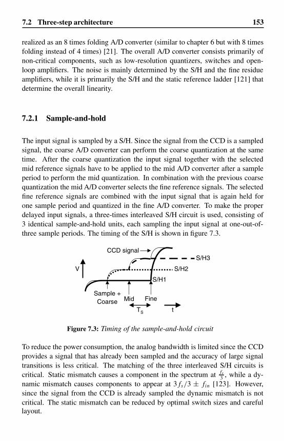
153
realized as an 8 times folding A/D converter (similar to chapter 6 but with 8 timesfolding instead of 4 times) [21]. The overall A/D converter consists primarily ofnon-critical components, such as low-resolution quantizers, switches and open-loop amplifiers. The noise is mainly determined by the S/H and the fine residueamplifiers, while it is primarily the S/H and the static reference ladder [121] thatdetermine the overall linearity.
7.2.1 Sample-and-hold
The input signal is sampled by a S/H. Since the signal from the CCD is a sampledsignal, the coarse A/D converter can perform the coarse quantization at the sametime. After the coarse quantization the input signal together with the selectedmid reference signals have to be applied to the mid A/D converter after a sampleperiod to perform the mid quantization. In combination with the previous coarsequantization the mid A/D converter selects the fine reference signals. The selectedfine reference signals are combined with the input signal that is again held forone sample period and quantized in the fine A/D converter. To make the properdelayed input signals, a three-times interleaved S/H circuit is used, consisting of3 identical sample-and-hold units, each sampling the input signal at one-out-of-three sample periods. The timing of the S/H is shown in figure 7.3.
S/H1
Sample +Coarse
CCD signal
Fine
S/H2
S/H3
Mid
TS
V
t
Figure 7.3: Timing of the sample-and-hold circuit
To reduce the power consumption, the analog bandwidth is limited since the CCDprovides a signal that has already been sampled and the accuracy of large signaltransitions is less critical. The matching of the three interleaved S/H circuits iscritical. Static mismatch causes a component in the spectrum at fs
3 , while a dy-namic mismatch causes components to appear at 3fs/3 ± fin [123]. However,since the signal from the CCD is already sampled the dynamic mismatch is notcritical. The static mismatch can be reduced by optimal switch sizes and careful
7.2 Three-step architecture
layout.

154
7.2.2 Resolution distribution
The resolution can be distributed over the three steps in several combinations. Theoptimum distribution for minimum total intrinsic capacitance is when the resolu-tions of the three steps are equal (similar to section 3.18). This results in 6 coarsebits, 6 mid bits and 6 fine bits. The total number of bits of the coarse, mid and fineA/D converter amounts to more than 16 bits since over-range is employed in themid and fine stage (section 3.4) [29]. This choice of resolutions requires 4 times2048 switches and taps on the reference ladder for the fine reference selection.This results in a large parasitic capacitance connected to the reference ladder. Toreduce the number of required switches the sum of the coarse and mid bits is re-duced, which results in an increased number of fine bits. This design uses 4 coarsebits, 5 mid bits and 9 fine bits. This requires 4 times 16 switches to select the midreferences and 4 times 256 switches for the selection of the fine references whichresults in a factor of 4 reduction in parasitic switch capacitance. The increasedaccuracy places demands on the fine A/D converter, which increases from 7 to9 bits, and is resolved by using a folding A/D converter. The INL of a foldingA/D converter depends mainly on the size of the input transistors of the foldingamplifiers (section 3.3). However, because of the folding amplifier gain, the DNLis small. In the imaging application DNL is more important than INL. This allowsfor smaller folding amplifier input devices that reduce the intrinsic capacitanceand therefore power.
7.2.3 Switching
The selection of the references for the mid conversion is made by translating thethermometer code of the coarse conversion to a
’
one-high’ code. This
’
one-high’signal selects the 4 proper reference signals from the static reference ladder (seechapter 6).
Since the selection of the references for the fine conversion requires 1 out of256 selection, special care has been taken. To avoid the need for an 8-bit binaryto
’
one-high’ encoder, the coarse quantization selects 1 out of 16 switch blocks,in which the mid quantization selects the 4 proper references. This is similar tothe matrix selection used in DACs [125]. Before the proper coarse selection can
A low-power16-bit three-step ADC for imaging applications

155
be made, the errors of the coarse quantization have to be corrected first. This isdone by using the under and over-range indicator of the mid A/D conversion andis shown in figure 7.4.
Coarse CODE
Under/Overrange Mid ADC
nrefBnrefA
refBrefA
finerefAfinenrefAfinerefBfinenrefB
HALF
MidCODE
nrefA
nrefB
Switch Unit
VRB
VRT
Ref
eren
ce
Ladd
er nrefBnrefA
refBrefA
refBrefA
nrefBnrefA
Figure 7.4: Fine switch matrix with selection of the fine reference signalsusing matrix encoding and reference symmetry
To reduce the number of switches required, the property of symmetry is used.When a certain fine subrange is selected, for example at the bottom of the range,references from the bottom and references from the top of the resistor ladder areselected since the input signal is differential. When the input signal is at the topof the range, the same references are selected but are applied inversely to thefine residue amplifiers. In this case the same reference selection is made, but thereferences are exchanged by a set of additional switches. This is also shown infigure 7.4. The inversion of the selection is indicated by the signal HALF. HALFis zero when the input signal is in the lower half of the input signal range andHALF is one when the input signal is in the upper half of the input signal range.The corresponding selected reference signals (before processing with the HALFsignal) are shown in figure 7.5. For the sake of simplicity the under-range andover-range have been omitted from this figure.
7.2 Three-step architecture

156
HALF
inp
innnrefA
refA
refB
nrefB
SUB(n)SUB(n+1)
nrefA
refA
Ref
eren
ce
Ladd
er
nrefA
nrefA
nrefB
refA
refB
refA
nrefB/refB
SUB(n+2)SUB(n+3)
nrefB nrefB
nrefA
refB refB
refA
input
VRB
VRT
Figure 7.5: Selected fine reference signals in the switch matrix before theinversion with the HALF signal (without over-range)
scribed in chapter 6. However, the selected signals are the same for the upper halfand the lower half of the input range, which results in only half the number ofselection switches being used.
7.3 Noise considerations
The S/H consists of three-times interleaved S/H units, as explained in section 7.2.Figure 7.6a and figure 7.6b show the sample and the hold phase, respectively, ofsuch a flip-around [56, 33] S/H unit.
During the sample phase (figure 7.6a), the OPAMP acts as a virtual ground. Thesampled noise in this case is given by equation 2.8, where Chold is the hold capa-citance and NEF is the noise excess factor [7] of the OPAMP. For more than 85 dBDRpp and an input signal swing of 2 V peak-to-peak differential, a capacitance of7.5 pF for Chold in figure 7.6 is sufficient.
A low-power16-bit three-step ADC for imaging applications
As shown in figure 7.5, the references are selected in a similar way to that de-

157
inp
inn
outp
outn
Chold
Chold
Chold
Chold
OPAMP OPAMP
Figure 7.6: The sample phase (a) and the hold phase (b) of a S/H unit
only instrumental for the fine reference selection. As a result, only the noisegenerated in the signal path to the fine comparators during the hold phase of theS/H is considered. During the hold phase (figure 7.6b) the hold capacitance isflipped around the OPAMP. During this phase the hold capacitance is not seen bythe OPAMP as a load capacitance and therefore does not filter the noise generatedby the OPAMP. The total noise power generated in the signal path during the holdphase is the sum of the noise generated by the OPAMP and the switches of theS/H, the reference ladder including switches, the residue amplifiers and the fineA/D converter. The effect of the latter is, however, reduced significantly by thegain in the residue amplifier stage. The noise generated during the hold phase ofthe S/H is sampled by the fine comparators. The gain in the signal path from theS/H up to the fine comparators reduces the accuracy requirements at the input ofthe fine comparators to less than 7 bit. The signal bandwidth at the comparatorinput is therefore limited with respect to the bandwidth of the S/H, resulting in afiltering of part of the noise coming from the S/H which is sampled by the finecomparators.
The accuracy requirements of the input stage of the S/H OPAMP and the residueamplifiers with respect to noise are similar. The noise contributions of these com-ponents are therefore similar for optimum power consumption. The noise contri-bution of the reference ladder is determined by the total resistance of the ladder.Reducing the ladder resistance increases the current through the ladder. Increasingthe width of the selection switches reduces their noise contribution but increasesthe capacitive load determined by the switches, reducing the settling speed of thereferences. The noise contribution of each of the components described has beendesigned for minimum power consumption. The contribution to the DRpp of eachcomponent is shown in table 7.2.
7.3 Noise considerations
(a) (b)
The coarse and mid quantization do not determine the final quantization and are

158
SHA SHA Ref ladder Res Amp A Res Amp B Fine ADC
Sample Hold
Block
DRpp
Sub total
Total
Phase
Table 7.2: Contribution of the thermal noise to the DRpp of the differentA/D converter blocks during the sample and hold phase
As can be seen, the contribution of both residue amplifiers is not equal. This isdependent on the position of the zero-crossing in the fine A/D converter. Close tothe beginning or the end of the fine range the noise is dominated by one amplifier,while in the middle of the fine range both residue amplifiers contribute equallyto the noise. The total DRpp of 93.0 dB during the hold phase in table 7.2 is notcalculated from the sum of the contributions of each block, but is the simulatedtotal value. The sum of the noise during the hold phase in table 7.2 results ina DRpp of 94.3 dB. This means that the remaining blocks of the A/D convertergenerate noise resulting in a DRpp of 98.8 dB. These remaining blocks include thechopping circuits and biasing. The total DRpp determined by thermal noise duringthe sample and the hold phase equals 90.4 dB. This gives some margin in thedesign with respect to other sources of noise, such as reduction due to comparatoroffset errors or substrate noise injection.
7.4 Mixed-signal chopping and calibration
7.4.1 Mid and fine residue amplifier stage calibration
The offsets of the mid residue amplifiers need to be below 128 LSB at 16-bitaccuracy to guarantee proper fine sub-range selection, while the offsets of the fineresidue amplifiers need to be below 1 LSB as this determines the accuracy of theADC. These low offset values are obtained by using MSCC, with digital offsetextraction and analog compensation [58]. The offset extraction of both mid andfine residue amplifier stages is performed simultaneously.
The coarse A/D converter quantizes the input signal and determines in which midsubrange the input signal is located. The corresponding references are selected bythe mid switch matrix and applied together with the input signal to the mid residue
A low-power16-bit three-step ADC for imaging applications
93.9 dB
93.9 dB
98.31 dB 100.2 dB
93.0 dB (total from noise simulation)
107.22 dB 99.48 dB 121.54 dB
90.4 dB

159
amplifiers. By chopping the input signals of these residue amplifiers, their offsetis detected using the digital output of the mid A/D converter. Chopping of thefine residue amplifiers is applied after the mid quantization is performed, as canbe seen in figure 7.2. The fine residue amplifier chopping does not therefore haveany effect on the mid quantization and the extraction of the mid residue amplifieroffset is performed independently of the chopping of the fine residue amplifiers.
Since the mid residue amplifier chopping is performed before the fine quantiz-ation, this can potentially influence the fine residue amplifier offset extraction.Below it is explained how the mid residue amplifier offset extraction and the fineresidue amplifier offset extraction do not influence each other.
The mid quantization determines the selected fine reference signals and choppingof the mid residue amplifier with offset may therefore lead to a different finesubrange (and fine reference signals) selection. The result is that for a certain inputsignal two different fine-residue signals can be applied to the fine A/D converter.This is illustrated in figure 7.7a.
Fine-residuesignal
SUB(n) SUB(n+1) SUB(n) SUB(n+1)
ADCoutput
input input
input input
Fine-residuesignal
ADCoutput
fine n fine n+1fine n fine n+1
Figure 7.7: Fine residue signal selection and A/D converter outputwithout (a) and with (b) fine residue amplifier offset
7.4 Mixed-signal chopping and calibration
(a) (b)
offset A
offset A

160
The residue signal fine(n) in figure 7.7a is the result of the selection of SUB(n)
by the mid A/D converter, while residue signal fine(n + 1) is the result of theselection of SUB(n + 1). Because there is overlap (redundancy) between the sub-ranges SUB(n) and SUB(n + 1), the same A/D converter output code is generated,independently of the result of the mid A/D converter.
When there is also an offset present at the input of the fine residue amplifiers,the corresponding residue signals of two subsequent subranges are shown in fig-ure 7.7b. In this case only amplifier A has an offset of offsetA. When, due tomid residue amplifier offset and chopping, two different subranges SUB(n) andSUB(n + 1) are selected for a certain input signal, this results in two different fineresidue signals fine(n) and fine(n + 1). However, due to fine residue amplifier off-set the overlap is not perfect, as is shown at the bottom of figure 7.7b. The totalA/D converter therefore has different output codes for constant input signal, illus-trated with the black dots in figure 7.7b. As can be seen, the chopping of the midresidue amplifiers changes the output of the A/D converter. However, the contri-bution of the offset of the fine residue amplifiers to the A/D converter output, withrespect to the ideal output, still results in a positive error. The fine residue amp-lifier offset extraction is therefore not disturbed, since the offset extraction onlydetects the sign of the offset.
7.4.2 Quick calibration
The MSCC only updates the DAC values after an integration period, which issufficiently long for reliable and accurate offset extraction. The MSCC thereforetakes over 106 samples to settle. For test purposes a quick foreground calibrationoption is integrated during fabrication for each MSCC; this can also be used atpower-up for a quick initial calibration. During quick calibration mode the inputsof the residue amplifiers are short-circuited and the digital extraction block appliesa binary search [87] for the proper compensation DAC codes. For the comparisonduring the binary search, the ladder buffers, pre-amplifiers and comparators ofthe normal operation mode are used. The quick calibration system of the residueamplifiers and the corresponding D/A converter signals of one calibration cycleare shown in figure 7.8.
Since the D/A converters for the mid and fine compensation are 9 and 11 bits,respectively, the quick calibration cycles take 9 and 11 clock cycles.
A low-power16-bit three-step ADC for imaging applications

161
ResAMPs
n-bitADC
DAC A
resA
nresA
Ic(0)
MSCC
Ic(2n)resB
nresB
DAC A
DAC B Quick calibration
mode
Optimal DAC A value
TS
DAC B
Optimal DAC B value
TS
t [s]
t [s]
Figure 7.8: Quick calibration system with calibration cycle example
7.5 Supply voltages
Most CMOS technologies offer dual gate oxide. For this design 0.18 µm CMOStechnology with 2 values for the gate oxide thickness was used. The (effective)oxide thickness determines the permitted supply voltage (thin oxide for 1.8 Vdevices and thick oxide for 3.3 V devices) and therefore the achievable signalswing. Figure 2.7 shows the relative dependence of the power as a function of the(effective) oxide thickness. For noise- and matching-limited designs the capacit-ance increases by 1
t2ox
and 1tox
respectively. To compare the power, it is assumedthat the bandwidth remains constant and Vgt scales linearly with Vdd . As is shownin figure 2.7, the power for a noise limited design is initially constant as a functionof tox . However, since the relation between Ids and Vgt is not linear for small Vgt ,for small tox the power becomes inversely proportional to
√tox for a noise-limited
design (which is also shown in figure 2.7). For a matching-limited design, thepower is initially proportional to tox , however for small Vgt , the power becomesproportional to
√tox . This is illustrated in figure 2.7. As this ADC has both noise-
limited and matching-limited parts, the optimum power dissipation is exploited byusing two different gate oxides. Figure 7.9 shows the block diagram of the A/Dconverter, with the supplies per block.
The capacitance of the S/H is determined by the noise requirements and is de-signed with the 3.3 V thick oxide transistors. The quantizing parts, which arematching limited, and the digital circuitry are designed with 1.8 V thin oxide tran-
7.5 Supply voltages
sistors. The power consumption of the 3.3 V and the 1.8 V part are now similar.

162
input
VRB
VRT
Ref
eren
ce
Ladd
er
ResAMPs
ResAMPs
3X Interleaved S/H
16 Bit
MSCC1
4-bitCoarseADC
SwitchMatrix
Latch Latch
Latch
MSCC2
SwitchMatrix
5-bitMidADC
9-bitFineADC
DecoderAnd
OverrangeCorrection
Figure 7.9: Block diagram with two separate supplies
Changing the 3.3 V supply into a 1.8 V supply would decrease the allowable sig-nal swing by a factor of 1.8. This would increase the required power consumptionby a factor of 1.3, since the capacitance is increased by this factor and in theOPAMP of the S/H input devices with small Vgt are used.
7.6 Experimental results
A die photograph of the three-step A/D converter is shown in figure 7.10.
The A/D converter is fabricated in standard single poly, five metal 0.18 µm CMOSand the core area is 1.4 mm2. The ADC operates at 1.8 V and 3.3 V supplyvoltages and dissipates 141 mW (without output buffers). The relative powerconsumption of each block is shown in figure 7.11.
The power consumption of the fine residue amplifiers is relatively large. This iscaused by the fact that these amplifiers have a large gain (≈64) in combinationwith a large signal bandwidth. The fine A/D converter power consumption isrelatively high since 9 bits are resolved in one step by a folding A/D converter.
For imaging applications, and in particular for a small input signal, the DRpp isvery important. Figure 7.12 shows the DRpp of the A/D converter, which is the
A low-power16-bit three-step ADC for imaging applications
1.8 V supply
3.3 V supply

163
Figure 7.10: Die photograph of the three-step 16-bit A/D converter
SHACoarse ADC
Mid Res Amps
Mid Ladder Buffer
Mid ADCFine Res AmpsFine Ladder
Buffer
Fine ADC
peak-to-peak signal to rms noise ratio for different input signal levels as a functionof the sample rate. The measurements have been performed with an input signalfrequency of 1 MHz.
When no input signal is applied, the DRpp of the A/D converter is calculated bydividing the peak-to-peak output code (which is 216) by the rms of the noisemeasured at the output of the A/D converter. This DRpp is above 88 dB up to30MSample/s, which is close to the calculated value from table 7.2. For low inputsignal levels, the DRpp is above 85 dB for sample rates up to 30 MSample/s. For
7.6 Experimental results
converterFigure 7.11: The relative power consumption of each block of the A/D
Digital

164
60
65
70
75
80
85
90
10,00 15,00 20,00 25,00 30,00 35,00 40,00 45,00
-? dBfs
26 dBfs
8 dBfs
2 dBfs
0 dBfs
FS [MHz]
DRpp [dB]dBfs
Input levelSpecification
Figure 7.12: DRpp for different input signal levels as a function of thesample rate (fin = 1 MHz)
larger input levels, the DRpp degrades further. A major artifact which causes thishas been found in the fine-residue stage. For large input signal amplitude (andrelatively high signal frequency), the fine reference change is large from sampleto sample. These large jumps in both references and sample-and-hold signal in-cidentally cause the output stage of the fine-residue amplifier stage to go out ofsaturation. Recovery from this requires too much time with respect to the highestsample rates, thus degrading the performance. This will be solved in a subsequentversion. A second effect is that the switching of the reference signals causes thereference ladder to be disturbed. However, in an imaging application the largesignal behavior is less important, since a performance reduction for high light in-tensities is less visible. Figure 7.13 shows the SINAD as a function of the inputsignal level for different sample rates (fin = 1 MHz).
As can be seen in figure 7.13, the SINAD increases as a function of the inputlevel. For high input levels, the SINAD reaches a maximum before the input levelis at maximum. This is also limited by the fine-residue amplifier stage and thelimited settling speed of the ladder. This is confirmed by the fact that the inputlevel where the SINAD is at maximum decreases for increasing sample rates. TheDNL and INL plots, obtained for a low-frequency input signal and sampled at15 MSample/s, are shown in figure 7.14 and figure 7.15. The number of pointsthat are used to calculate the DNL and INL is 32000000.
As is shown in figure 7.12, the large signal performance at a sample rate of30 MSample/s is limited. Since this would also limit the DNL and INL measure-ment, a sample rate of 15 MSample/s is used to measure the DNL and INL. The
A low-power16-bit three-step ADC for imaging applications
–
–
–
–

165
Figure 7.13: SINAD as a function of the input signal level for differentsample rates (fin = 1 MHz)
Figure 7.14: DNL measured with a signal frequency of 230 Hz and15 MSample/s
Figure 7.15: INL measured with a signal frequency of 230 Hz and15 MSample/s
7.6 Experimental results

166
A/D converter has no missing codes since the DNL remains just above 1 LSB.The incidental peaks in DNL above +1 LSB are most probably caused by thermalnoise. The INL is between 13 LSB and +13 LSB, which is sufficient for the ap-plication. In order to calculate the FoM of this converter, the resolution bandwidthhas to be determined. The measurement of the SINAD as a function of the signalfrequency for different signal levels is shown in figure 7.16.
0
10
20
30
40
50
60
70
80
0,00 2,00 4,00 6,00 8,00 10,00 12,00
26 dBfs
8 dBfs
2 dBfs
0 dBfs
fin
SINAD [dB]
Input level
Figure 7.16: SINAD as a function of the input signal frequency for differentsignal levels (fS = 20 MSample/s)
Since the resolution bandwidth of this converter is limited to ≈2 MHz, the FoMis 19.7 pJ/conv. When the FoM is corrected for the input signal swing of 2 Vpeak-to-peak, the resulting FoMVpp equals 79.1 pJV2/conv. The performance is
Resolution 16 bit
SINAD (max)
Sample Rate
DNL
INL
Power dissipation
Area
Technology
68 dB
30 MSample/s
1 LSB < DNL < 1.1 LSB (no missing codes)
13 LSB < INL < 13 LSB
141 mW
1.4 mm2
5M1P 0.18 µm CMOS
DRpp ADC 77 dB (input signal 2 dBfs)
DRpp ADC 88 dB (no input signal)
Input range 2 Vpp, differential
Table 7.3: Summarized performance
A low-power16-bit three-step ADC for imaging applications
−
−
summarized in table 6.2.
−−
−
–
–
–
[MHz]
167
An A/D converter [126] for a similar application has shown a smaller samplefrequency of 20 MSample/s and a larger power consumption of 300 mW (whichincludes the correlated double sampling circuit (CDS) and a programmable gainamplifier).
7.7 Discussion
This realization shows that the MSCC can be used in a
’
more-step’ configurationand is not limited to a two-step architecture. Together with dual-residue signalprocessing the use of MSCC relaxes the demands on the inter-stage residue ampli-fiers. The achieved DRpp is 88 dB according to the specification. The DNL showsthat the converter is monotonic, since the DNL is always larger than 1 LSB. Sincethe rms of the thermal noise voltage is about 2.5 LSB, a large number of points isused in the DNL calculation. However, this may still incidentally cause the DNLto be larger than 1 LSB.
The generation of 16 bits requires that 216 levels are distinguished. To limit thenumber of comparators this is done in three steps. In this design, this does, how-ever, still require 256 subranges to be selected from a reference ladder. Thiscauses a large capacitive load of the reference selection switches to be connec-ted to the reference ladders, which limits the achievable speed and input signalfrequency. However, the sampling speed is sufficient for the imaging applicationand the performance for high input signal frequencies is not important. The speedcould be improved by reducing the number of selected references by employingre-sampling of the analog signal after the gain stages. This would result in a morepipe-lined structure.
Because of the optimizations with respect to the input signal properties, such ashigh performance for small input signal levels and low performance for high inputsignal levels, the power is 141 mW. The large signal amplitude and high signalfrequency performance is limited by slow recovery from over-drive at the outputstage of the fine residue amplifier stage in this version of the 16-bit A/D converter.In the next version the output stage of the residue amplifier will be improved,increasing the resolution bandwidth. This will improve both the realized FoM andFoMVpp since the improvement does not increase the power consumption.
7.7 Discussion
−

168
7.8 Conclusions
The experiment in this chapter has shown that dual-residue signal processing withMSCC enables the design of a low-power A/D converter for imaging applications.The quantization is split up into three steps, reducing the accuracy requirementsand power of the sub A/D converters. Due to the dual-residue signal processingand MSCC the A/D converter has no missing codes at 16-bit level even with theuse of residue amplifiers with relatively small input devices and without an ac-curate gain factor. This is demonstrated in the DNL measurement. The DRpp
achieved is 88 dB in 15 MHz bandwidth for small input signal amplitudes at apower consumption of 141 mW. The performance degrades for larger input signalamplitudes, which is no limitation for the imaging application.
In addition to repairing the output stage of the fine residue amplifier stage in thisversion, an increase in the performance for larger input signal amplitudes andfrequencies would require more power. The selection of the references in partic-ular puts a limit on the high-frequency behavior. This A/D converter has beenoptimized for sampled input signals. When applying non-sampled signals the in-terleaved sample-and-hold probably has to be extended to a four-times interleavedsample-and-hold.
A low-power16-bit three-step ADC for imaging applications

Chapter 8
Conclusions
Analog-to-digital conversion is the key technology for embedded signal processing.Bandwidth, accuracy and power are the main parameters that determine A/D con-verter performance. This book investigates calibration techniques to increase theaccuracy of A/D converters while maintaining an acceptable power consumptionfor consumer applications.
Chapter 2 discusses the relation between accuracy and capacitance. Given thetechnology, the minimum required capacitances in an A/D converter are determ-ined for both the noise and the matching requirements. The resulting capacitancesderived from both the noise and the matching demands are quadratically depend-ent on the required accuracy. The maximum of these capacitances determinesthe required capacitance and is A/D-converter-architecure dependent. This re-quired capacitance needs to be charged with the respective signal with sufficientaccuracy within a certain time period, which is a measure for the power consump-tion. The power consumption of a circuit is proportional to the load capacitanceand inversely proportional to the available settling time, if the parasitic capacit-ance is smaller than the aforementioned load capacitance. When the availablesettling time approaches its lower limit, which means that the parasitic capacit-ance reaches the load capacitance, the power consumption is no longer inverselyproportional to the available settling time, but increases dramatically.
The errors caused by matching errors can be reduced by using calibration tech-niques. The capacitance resulting from matching requirements can therefore bedecreased, increasing the power efficiency of the A/D converter. However, since
169

170
noise is a random process, it cannot be calibrated and the capacitance determinedby the noise requirements is the lower limit and cannot be reduced by calibration.
It is beneficial to use the most advanced technology for A/D converter designs,which are matching-limited. The effect of the decreasing power supply voltage re-duces the allowed signal swing. However, the matching parameter AVT
decreasesas well. For noise-limited designs, the input signal amplitude should be as large aspossible, which demands for older technologies with larger supply voltages. Themaximum speed is achieved in the most advanced technologies, where the ratiobetween gm and the parasitic capacitance generally increases.
The choice for an A/D-converter architecture allows a trade-off to be made betweenaccuracy, speed and power. For low sample rates the architectures that reduce thenumber of necessary accurate devices are much more power-efficient than theparallel architectures. This is especially the case for high accuracy, where therequired capacitance becomes impractical. However, high-sample-rate parallelarchitectures are more power-efficient for low accuracy, since the conversion isdone in only one step. Practical realizations confirm this.
Higher-accuracy A/D conversion requires multi-stage architectures. When morebits in the first stage are applied, the accuracy in the least significant stages be-comes less critical. Therefore, generating more bits in the first stage(s) reducesthe accuracy requirements to only those of the first stage(s). This is in contrast tothe parallel architectures where all the decision blocks need high accuracy.
Even in multi-stage architectures straightforwardly increasing the accuracy wouldlead to high power consumption. Therefore, designing A/D converters for highaccuracy requires some form of calibration. Chapter 4 analyzes enhancementtechniques for the two-step architecture to increase the accuracy without increas-ing the power consumption.
In multi-stage architectures gain errors are the dominant accuracy-limiting factors.Chapter 4 introduces the dual-residue signal-processing technique to circumventthese errors. When improved switching is used, continuity and monotonicity areguaranteed. The difference in offset of the two dual-residue amplifiers determinesthe INL of the overall A/D converter. For high accuracy this means that the inputdevices of the amplifier need to be large to ensure a sufficiently low offset voltage.To reduce the input capacitance of the residue amplifiers, calibration is applied.
Conclusions

171
This technique uses only very few additional non-critical analog-components. Itdoes not require additional calibration time and operates under normal conversionconditions. Therefore, the calibration can be performed continuously without in-terfering with the normal operation of the A/D converter. The signal processingcapability of the digital CMOS technology is used to make large time-constantsenabling highly accurate offset extraction. In contrast to other calibration tech-niques, the MSCC technique requires no additional post-processing of the digitaloutput data and does not impair any timing parameter. The only overhead consistsof some regular updating of the integrators.
The first experiment in chapter 5 shows the dual-residue signal processing in com-
is the result of the combination of A/D conversion and offset cancellation in oneclock cycle.
The benefits of dual-residue signal processing in combination with MSCC is veri-fied in the second experiment in chapter 6. It is shown that the accuracy problemsin CMOS A/D converters are improved without impairing the sample rate, as wasthe case in the first experiment, or requiring excessive power. Even though simpleopen-loop residue amplifiers with relatively small input devices have been used,without special care for an exact gain factor, the MSCC reduces the offset voltagesof the residue amplifiers to a sufficiently low level.
The experiment in chapter 7 shows that dual-residue signal processing with MSCCenables the design of a low-power A/D converter for imaging applications. Thequantization is split-up into three-steps, reducing the accuracy requirements andpower consumption of the sub A/D converters. Due to the dual-residue signalprocessing and MSCC the A/D converter has no missing codes at 16-bit level,even with the use of residue amplifiers with relatively small input devices andwithout an accurate gain factor. The performance degrades for larger input signalamplitudes, which is no limitation for the imaging application. Increasing the per-formance for larger input signal amplitudes and frequencies would require morepower.
bination with analog offset calibration. Benchmarked with realizations in literature,the power consumption in this experiment is still too high, but the performancemeets the requirements for CVBS video signal processing, which is used as avehicle. The limitation of the calibration implementation in the first experiment
The mixed-signal chopping and calibration technique (MSCC) enables offset ex-traction from the output data in the digital domain and compensation in the ana-log domain, resulting in an A/D converter with almost perfect analog circuitry.
Conclusions

172
post-processing of the output data. The methods developed in this book seemapplicable for other circuit applications as well.
This book shows that accuracy in high-speed A/D converters can be optimizedwithout sample rate or power penalties. Moreover, there is no need for extensive
Conclusions

Appendix A
Static and dynamic accuracyrequirements
In this appendix the effect of static and dynamic errors on the performance degrad-ation are calculated. With this result a maximum allowable error in the quantiza-tion is derived to limit the performance degradation to an acceptable level.
A.1 Static error requirments
To calculate the maximum allowable static errors, the effect of random errorson the transfer curve of the A/D converter (INL) is calculated. Since the effect ofrandom errors on the transfer curve is similar to the effect of quantization noise onthe transfer curve of the A/D converter, the noise power representing the randomerrors can be added to the error power caused by quantization (similar to [1]):
SNRQ+error = 10 log
(32 22N
1 + 12σ 2error
), (A.1)
where σ is the standard deviation of the random errors and N is the number of bits.For an A/D converter this is equal to the standard deviation of the INL of eachindividual code. Subtracting the quantization noise from equation A.1 results inthe reduction of SNR caused by INL errors:
173

174
SNRred = −10 log(1 + 12σ 2
error
)(A.2)
When these INL errors are random errors with a gaussian distribution, the relationbetween σ of the errors and the maximum INL is given by:
σ 2error = INL2
α2, (A.3)
where α is the threshold value for the stochastic variable of the probability that themaximum random error remains within the limits ( INL, +INL) is acceptable [1].Depending on the number of critical components, α is in the range of three andfive. In chapter 3 it is derived that for the scope of this book it is sufficient to set α
to the constant value 4. Combining equation A.2 and equation A.3 results in thereduction of SNR caused by random gaussian distributed INL errors:
SNRred = −10 log
(1 + 12
INL2
α2
)(A.4)
To calculate the reduction in ENOB as function of the INL, equation A.4 is thenrewritten to:
ENOBred =− log
(1 + 12 INL2
α2
)2 log 2
(A.5)
The reduction in ENOB for a certain maximum INL is dependant on the distri-bution (shape) of the INL errors. The worst case situation occurs when the eachindividual INL error is equal to +INL or INL. In that case, σ 2
error = INL2 andequation A.5 changes into:
ENOBMAX red = − log(1 + 12 INL2
)2 log 2
(A.6)
Figure A.1 shows both ENOBred and ENOBMAX red as function of the INL. Also theresult of a Monte Carlo analysis is shown. In this analysis, the INL is randomlydetermined. The x-axis shows the maximum INL, while the y-axis shows the
Static and dynamic accuracy requirements
−
−

175
reduction in ENOB. In the calculation of ENOBred, the value for α is 3, whichmeans that the INL used in figure A.1 is the 3σ value of the distribution of theINL.
INL [LSB]
ENOBred
ENOBMAX red
ENOBred
ENOBMonte Carlo red
Figure A.1: Reduction in ENOB for: a random INL (with α = 3), onlyvalue of +INL or INL, and a Monte Carlo simulation, asfunction of INL
Figure A.1 shows that when the INL is less then ±0.25 LSB the overall perform-ance decreases at maximum with 0.4 ENOB (or 2.4 dB). This is the case when
0.25 LSB (on the curve ENOBMAX red
loss of 0.4 ENOB is used in the calculations as allowed performance degradation.This means that all errors due to the signal processing such as settling or mismatcherrors should remain within ±0.25 LSB. In practice the INL-pattern will also con-tain values ±0.25 LSB, which means the practical preformance degradation is inthe order of 0.2 ENOB (on the curve ENOBMonte Carlo red).
A.2 Dynamic error requirements
To keep the SNR reduction due to thermal noise (equation 2.12) sufficient low, inthis book it is assumed that the signal-to-thermal-noise ratio is 6 dB better thanthe signal-to-quantization-noise ratio. This results in an overall SNR reduction of1 dB, which is comparable to the reduction in SNR due to static INL errors, whenthe INL remains within ±0.25 LSB.
A.2 Dynamic error requirements
−
− ). In the remainder of this book the maximumthe INL-pattern of the A/D converter consists of only the values +0.25 LSB and

References
[1]
Circuits, vol. 29, pp. 879–886, 1994.
[2] J. van Lammeren, The design of low-cost one-chip TV systems. PhD thesis,Universiteit Twente, 2000.
[3] C. Mangelsdorf, H. Malik, S. Lee, S. Hisano, and M. Martin, “A two-residue architecture for multistage ADC’s,” ISSCC Digest of Technical Pa-pers, pp. 64–65, 1993.
[4] M. Pelgrom, A. Duinmaijer, and A. Welbers, “Matching properties of MOStransistors,” IEEE J. Solid-State Circuits, vol. 24, pp. 1433–1440, 1989.
[5] M. Pelgrom, H. Tuinhout, and M. Vertregt, “Transistor matching in analogapplications,” IEDM Technical Digest, pp. 34.1.1–34.1.4, 1998.
[6] A. Scholten, H. Tromp, L. Tiemeijer, R. van Langevelde, R. Havens,P. de Vreede, R. Roes, P. Woerlee, A. Montree, and D. Klaassen, “Accuratethermal noise model for deep-submicron CMOS,” IEDM Technical Digest,pp. 155–158, 1999.
[7] K. Laker and W. Sansen, Design of analog integrated circuits and systems.New York: McGraw-Hill, 1994.
[8]in Analog circuit design (J. Huijsing, M. Steyaert, and A. van Roermund,
[9] B. Razavi, Design of analog CMOS integrated circuits. New York:McGraw-Hill, 2001.
177
M. Pelgrom, J. van Rens, M. Vertregt, and M. Dijkstra, “A 25-MS/s 8-bitCMOS A/D converter for embedded application,” IEEE J. Solid-State
M. Vertregt and P. Scholtens, “Scalable high speed analog circuit design,”
eds.), pp. 3–21, Kluwer Academic Publishers, 2004.

178 References
[10] D. R. Breuer, “High-speed A/D converter monolithic techniques,” ISSCCDigest of Technical Papers, pp. 146–147, 1972.
[11] R. A. Nordstrom, “High-speed integrated A/D converter,” ISSCC Digest ofTechnical Papers, pp. 150–151, 1976.
[12] J. G. Peterson, “A monolithic video A/D converter,” IEEE J. Solid-StateCircuits, vol. 6, pp. 932–937, 1979.
[13] G. Geelen, “A 6b 1.1GSample/s CMOS A/D converter,” ISSCC Digest ofTechnical Papers, pp. 128–129, 2001.
[14] P. Scholtens and M. Vertregt, “A 6-bit 1.6-GS/s flash ADC in 0.18-µmCMOS using averaging termination,” IEEE J. Solid-State Circuits, vol. 37,pp. 1599–1609, 2002.
[15] C. Lane, “A 10-bit 60 MSps flash ADC,” Proc. BTCM, pp. 44–47, 1989.
[16] A. Venes and R. van de Plassche, “An 80-MHz, 80-mW, 8-b CMOS fold-
[17] K. Kattmann and J. Barrow, “A technique for reducing differential nonlin-earity errors in flash A/D converters,” ISSCC Digest of Technical Papers,pp. 170–171, 1991.
[18] K. Kusumoto, A. Matsuzawa, and K. Murata, “A 10-b 20-MHz 30-mWpipelined interpolating CMOS ADC,” IEEE J. Solid-State Circuits, vol. 28,pp. 1200–1206, 1993.
[19]2
[20]
[21] J. van Valburg and R. van de Plassche, “An 8-b 650-MHz folding ADC,”IEEE J. Solid-State Circuits, vol. 27, pp. 1662–1666, 1992.
incorporating folding and interpolation techniques,” IEEE J. Solid-StateCircuits, vol. 22, pp. 944–953, 1987.
J. Solid-State Circuits, vol. 31, pp. 1846–1853, 1996.ing A/D converter with distributed track-and-hold preprocessing,” IEEE
R. van de Grift, I. Rutten, and M. van der Veen, “An 8-bit video ADC
pp. 1302 1308, 1995.–and interpolating A/D converter,” IEEE J. Solid-State Circuits, vol. 30,
[22] B. Nauta and A. Venes, “A 70-MS/s 110-mW 8-b CMOS folding
ADC in 1 mm ,” IEEE J. Solid-State Circuits, vol. 32, pp. 1887–1895, 1997.K.Bult and A. Buchwald, “An embedded 240-mW 10-b 50 MS/s CMOS

References 179
[23] P. Vorenkamp and R. Roovers, “A 12-b, 60-MSample/s cascaded foldingand interpolating ADC,” IEEE J. Solid-State Circuits, vol. 32, pp. 1876–1886, 1997.
[24] G. Hoogzaad and R. Roovers, “A 65-mW, 10-bit, 40-MSample/s BiCMOSNyquist ADC in 0.8 mm2,” IEEE J. Solid-State Circuits, vol. 34, pp. 1796–1802, 1999.
[25] R. J. van de Plassche and R. E. J. van der Grift, “A high-speed 7 bit A/Dconverter,” IEEE J. Solid-State Circuits, vol. 6, pp. 938–943, 1979.
[26] A. Dingwall and V. Zazzu, “An 8-MHz CMOS subranging 8-bit A/D con-verter,” IEEE J. Solid-State Circuits, vol. 20, pp. 1138–1143, 1985.
[27] C. Moreland, F. Murden, M. Elliott, J. Young, M. Hensley, and R. Stop,“A 14-bit 100-MSample/s subranging ADC,” IEEE J. Solid-State Circuits,vol. 35, pp. 1791–1798, 2000.
[28] H. van der Ploeg and R. Remmers, “A 3.3-V, 10-b, 25-MSample/s two-stepADC in 0.35-µm CMOS,” IEEE J. Solid-State Circuits, vol. 34, pp. 1803–1811, 1999.
[29] S. Lewis and P. Gray, “A pipelined 5-MSample/s 9-bit analog-to-digitalconverter,” IEEE J. Solid-State Circuits, vol. 22, pp. 954–961, 1987.
[30] I. Mehr and L. Singer, “A 55-mW, 10-bit, 40-MSample/s Nyquist-rateCMOS ADC,” IEEE J. Solid-State Circuits, vol. 35, pp. 318–325, 2000.
[31] D. Cline and P. Gray, “A power optimized 13-b 5 MSample/s pipelinedAnalog-to-digital converter in 1.2 CMOS,” IEEE J. Solid-State Cir-cuits, vol. 31, pp. 294–303, 1996.
[32] J.-B. Shyu, G. Temes, and K. Yao, “Random errors in MOS capacitors,”IEEE J. Solid-State Circuits, vol. 6, pp. 1070–1076, 1982.
[34] A. Abo and P. Gray, “A 1.5-V, 10-bit, 14.3-MS/s CMOS pipeline anlog-to-digital converter,” IEEE J. Solid-State Circuits, vol. 34, pp. 599–606,1999.
µm
14b 75-Msample/s CMOS ADC with85-dB SFDR at Nyquist input,” IEEEJ. Solid-State Circuits, vol. 36, pp. 1931–1936, 2001.
[33] W. Yang, D. Kelly, I. Mehr, M. Sayuk, and L. Singer, “A 3-V 340-mW

180 References
[35]
pp. 38–39, 2000.
[36] D. Kelly, I. Mehr, M. Sayuk, and L. Singer, “A 3V 340mW 14b 75MSps
Papers, pp. 134–135, 2001.
[37] B. Murmann and B. Boser, “A 12-bit 75MS/s pipelined ADC using open-
2050, 2003.
[38] J. McCreary and P. Gray, “All-MOS charge redistribution analog-to-digital conversion techniques-part I,” IEEE J. Solid-State Circuits, vol. 10,pp. 371–379, 1975.
[39] K. Bacrania, “A 12-bit succesive-approximation-type ADC with digital er-ror correction,” IEEE J. Solid-State Circuits, vol. 21, pp. 1016–1025, 1986.
[40]ADC in 0.13µm CMOS,” ISSCC Digest of Technical Papers, pp. 176–177,2002.
[41] J. Lin and B. Haroun, “An embedded 0.8 V/480 µW 6b/22 MHz flash ADCin 0.13-µm digital CMOS process using a nonlinear double interpolationtechnique,” IEEE J. Solid-State Circuits, vol. 37, pp. 1610–1617, 2002.
[42]ADC in 0.3 mm2,” ISSCC Digest of Technical Papers, pp. 170–171, 2002.
[43] C. Donovan and M. Flynn, “A
”
IEEE J. Solid-State Circuits, vol. 37, pp. 432–437, 2002.
[44] I. Mehr and D. Dalton, “A 500-MSample/s, 6-bit Nyquist-rate ADC fordisk-drive read-channel applications,” IEEE J. Solid-State Circuits, vol. 34,pp. 912–920, 1999.
[45] K. Nagaraj, D. Martin, M. Wolfe, R. Chattopadhyay, S. Pavan, J. Cancio,and T. Viswanathan, “A dual-mode 700-MSample/s 6-bit 200-MSample/s7-bit A/D converter in a 0.25-µm digital CMOS process,” IEEE J. Solid-State Circuits, vol. 35, pp. 1760–1768, 2000.
[46]CMOS,” IEEE J. Solid-State Circuits, vol. 36, pp. 1847–1858, 2001.
digital” 6-bit ADC in 0.25-µm CMOS,”
L. Singer, S. Ho, M. Timko, and D. Kelly, “A 12 b 65 MSample/s CMOS
F. Kuttner, “A 1.2 V 10 b 20 MSample/s non-binary succesive approximation
K. Sushihara and A. Matsuzawa, “A 7 b 450 MSample/s 50 mW CMOS
M. Choi and A. Abidi, “A 6 b 1.3 GSample/s A/D converter in 0.35 µm
ADC with 82 dB SFDR at 120MHz,” ISSCC Digest of Technical Papers,
CMOS ADC with 85dB SFDR at Nyquist,” ISSCC Digest of Technical
loop residue amplification,” IEEE J. Solid-State Circuits, vol. 38, pp. 2040–

References 181
[47] K. Nagaraj, F. Chen, T. Le, and T. R. Viswanathan, “Efficient 6-bit A/Dconverter using a 1-bit folding front end,” IEEE J. Solid-State Circuits,vol. 34, pp. 1056–1062, 1999.
[48] K. Uyttenhove, J. Vandenbussche, E. Lauwers, G. Gielen, and M. Steyaert,“Design techniques and implementation of an 8-bit 200-MS/s interpolat-ing/averaging CMOS A/D converter,” IEEE J. Solid-State Circuits, vol. 38,pp. 483–494, 2003.
[49]8b Self-Calibrating Folding ADC with 7.26 ENOB at Nyquist Frequency,”ISSCC Digest of Technical Papers, vol. 47, pp. 252–253, 2004.
[50]Converter Using an Amplifier Preset Technique,” ISSCC Digest of Tech-nical Papers, vol. 47, pp. 254–255, 2004.
[51]folding ADC for gigabit ethernet LSI,” VLSI Digest of Technical Papers,pp. 212–213, 2000.
[52] M.-H. Liu and S.-I. Liu, “An 8-bit 10 MS/s folding and interpolating ADCusing the continous-time auto-zero technique,” IEEE J. Solid-State Cir-cuits, vol. 36, pp. 122–128, 2001.
[53] Y. Li and E. Sanchez-Sinencio, “A wide input bandwidth 7-bit 300-MSample/s folding and current-mode interpolating ADC,” IEEE J. Solid-State Circuits, vol. 38, pp. 1405–1410, 2003.
[54] R. Taft and M. Tursi, “A 100-MS/s 8-b CMOS subranging ADC with sus-tained parametric performance from 3.8 V down to 2.2 V,” IEEE J. Solid-State Circuits, vol. 36, pp. 331–338, 2001.
[55] B. Brandt and J. Lutsky, “A 75-mW. 10-b, 20-MSPS CMOS subrangingADC with 9.5 effective bits at Nyquist,” IEEE J. Solid-State Circuits,vol. 34, pp. 1788–1795, 1999.
[56]
[57] M.-J. Choe, B.-S. Song, and K. Bacrania, “A 13-b 40-MSamples/s CMOSpipelined folding ADC with background offset trimming,” IEEE J. Solid-State Circuits, vol. 35, pp. 1781–1790, 2000.
50-MS/s A/D converter in 0.6-µm CMOS with over 80-dB SFDR,” IEEEJ. Solid-State Circuits, vol. 35, pp. 1769–1780, 2000.
H. Pan, M. Segami, M. Choi, J. Cao, and A. Abidi, “A 3.3-V 12-b
R. Taft, C. Menkus, M. Tursi, O. Hidri, and V. Pons, “A 1.8 V 1.6 GS/s
G. Geelen and E. Paulus, “An 8 b 600 MS/s 200 mW CMOS Folding A/D
K. Yoon, J. Lee, D.-K. Jeong, and W. Kim, “An 8-bit 125 MS/s CMOS

182 References
[58] H. van der Ploeg, G. Hoogzaad, H. Termeer, M. Vertregt, and R. Roovers,2
signal chopping and calibration,” IEEE J. Solid-State Circuits, vol. 36,pp. 1859–1867, 2001.
[59] B. Hernes, A. Briskemyr, T. Andersen, F. Telstø, T. Bonnerud, and
Digital CMOS,” ISSCC Digest of Technical Papers, vol. 47, pp. 256–257,2004.
[60]“
[61] K. Poulton, R. Neff, B. Setterberg, B. Wuppermann, T. Kopley, R. Jew-
319, 2003.
[62]
[63] K. Kaviani, O. Oralkan, P. Khuri-Yakub, and B. Wooley, “A multichannelpipeline analog-to-digital converter for an integrated 3-D ultrasound ima-ging system,” IEEE J. Solid-State Circuits, vol. 38, pp. 1266–1270, 2003.
[64] D. Miyazaki, S. Kawahito, and M. Furuta, “A 10-b 30-MS/s low-powerpipelined CMOS A/D converter using a pseudodifferential architecture,”IEEE J. Solid-State Circuits, vol. 38, pp. 369–373, 2003.
[65] Y.-I. Park, S. Karthikeyan, F. Tsay, and E. Bartolome, “A
Digest of Technical Papers, pp. 130–131, 2001.
[66]pipelined A/D converter using a pseudo-differential architecture,” ISSCCDigest of Technical Papers, pp. 174–175, 2002.
[67] B.-M. Min, P. Kim, F. Bowman, D. Boisvert, and A. Aude, “A 69-mW 10-bit 80-MSample/s pipelined CMOS ADC,” IEEE J. Solid-State Circuits,vol. 38, pp. 2031–2039, 2003.
APapers, pp. 166–167, 2002.
K. Poulton, R. Neff, A. Muto, W. Liu, A. Burstein, and M. Heshami,
lined ADC,” ISSCC Digest of Technical Papers, pp. 326–327, 2003.
S.-M. Yoo, J.-B. Park, H.-S. Yang, H.-H. Bae, K.-H. Moon, H.-J. Park,
“A 2.5-V 12-b 54-MSample/s 0.25-µm CMOS ADC in 1 mm with mixed-
O. Moldsvor, “A 1.2V 220MS/s 10b Pipeline ADC Implemented in 0.13 m
4 GSample/s 8b ADC in 0.35 µm CMOS,” ISSCC Digest of Technical
memory in 0.18 µm CMOS,” ISSCC Digest of Technical Papers, pp. 318–
S.-H. Lee, and J.-H. Kim, “A 10 b 150 MS/s 123 mW 0.18 µm CMOS pipe-
10 b100 MSample/s CMOS pipelined ADC with 1.8 V power supply,” ISSCC
D. Miyazaki, M. Furuta, and S. Kawahito, “A 16 mW 30 MSample/s 10 b
ett, J. Pernillo, C. Tan, and A. Montijo, “A 20 GS/s 8 b ADC with a 1 MB

References 183
[68] K. Irie, N. Kusayanagi, T. Kawachi, T. Nishibu, and Y. Matsumori, “An
Papers, pp. 77–78, 1999.
[69]with Digital Background Calibration,” ISSCC Digest of Technical Papers,vol. 47, pp. 454–455, 2004.
[70] I. Opris, L. Lewicki, and B. Wong, “A single-ended 12-bit 20 MSample/sself-calibrating pipeline A/D converter,” IEEE J. Solid-State Circuits,vol. 33, pp. 1898–1903, 1998.
[71] J. Ingino and B. Wooley, “A continuously calibrated 12-b 10-MS/s, 3.3-VA/D converter,” IEEE J. Solid-State Circuits, vol. 33, pp. 1920–1931, 1998.
[72] A. Shabra and H.-S. Lee, “Oversampled pipeline A/D converters with mis-match shaping,” IEEE J. Solid-State Circuits, vol. 37, pp. 566–578, 2002.
[73]pipelined ADC,” ISSCC Digest of Technical Papers, pp. 46–47, 2000.
[74]low DNL,” IEEE J. Solid-State Circuits, vol. 35, pp. 281–285, 2000.
[75]Pipeline A/D Converter,” ISSCC Digest of Technical Papers, vol. 47,pp. 456–457, 2004.
[76]
[77]
vol. 47, pp. 458–459, 2004.
[78]Pipelined ADC,” ISSCC Digest of Technical Papers, vol. 47, pp. 452–453,2004.
[79]VLSI Digest of Technical Papers, pp. 208–211, 2000.
Papers, vol. 47, pp. 258–259, 2004.
8 b 500 MS/s full Nyquist cascade A/D converter,” VLSI Digest of Technical
H.-C. Liu, Z.-M. Lee, and J.-T. Wu, “A 15 b 20 MS/s CMOS Pipelined ADC
H.-S. Chen, K. Bacrania, and B.-S. Song, “A 14 b 20 MSample/s CMOS
I. Opris, B. Wong, and S. Chin, “A pipeline A/D converter architecture with
K. Nair and R. Harjani, “A 96 dB SFDR 50 MS/s Digitally Enhanced CMOS
S. Limotyrakis, S. Kulchycki, D. Su, and B. Wooley, “A 150 MS/s 8 b 71 mWTime-Interleaved ADC in 0.18 m CMOS,” ISSCC Digest of Technical
Y. Chiu, P. Gray, and B. Nikolic, “A 1.8 V 14 b 10 MS/s Pipelined ADC
E. Siragusa and I. Galton, “A Digitally Enhanced 1.8 V 15 b 40 MS/s CMOS
in 0.18 m CMOS with 99 dB SFDR,” ISSCC Digest of Technical Papers,
C. Michalski, “A 12 b 105 MSample/s, 850 mW analog to digital converter,”

184 References
[80] J. Sauerbrey, D. Schmitt-Landsiedel, and R. Thewes, “A 0.5-V 1-µWsuccessive approximation ADC,” IEEE J. Solid-State Circuits, vol. 38,pp. 1261–1265, 2003.
[81] M. Scott, B. Boser, and K. Pister, “An ultralow-energy ADC for smartdust,” IEEE J. Solid-State Circuits, vol. 38, pp. 1123–1129, 2003.
[82] E. Blecker, T. McDonald, O. Erdogan, P. Hurst, and S. Lewis, “Digitalbackground calibration of an algorithmic analog-to-digital converter usinga simplified queue,” IEEE J. Solid-State Circuits, vol. 38, pp. 1059–1062,2003.
[83] P. Rombouts, W. de Bilde, and L. Weyten, “A 13.5-b 1.2-V micropowerextended counting A/D converter,” IEEE J. Solid-State Circuits, vol. 36,pp. 176–183, 2001.
[84] O. Erdogan, P. Hurst, and S. Lewis, “A 12-b digital-background-calibratedalgorithmic ADC with -90-dB THD,” IEEE J. Solid-State Circuits, vol. 34,pp. 1812–1820, 1999.
[85] M. Pelgrom, “A 10-b 50-MHz CMOS D/A Converter with 75� Buffer,”IEEE J. Solid-State Circuits, vol. 25, pp. 1347–1352, 19910.
[86] H. P. Tuinhout, G. Hoogzaad, M. Vertregt, R. L. J. Roovers, and C. Erd-mann, “Design and characterization of a high-precision resistor ladder teststructure,” IEEE Transactions on Semiconductor Manufacturing, vol. 16,pp. 187–193, 2003.
[87] B. Razavi, Principles of data conversion system design. Piscataway: IEEEPress, 1995.
[88] T. Shimizu, M. Hotta, K. Maio, and S. Ueda, “A 10-bit 20-MHz two-stepparallel A/D converter with internal S/H,” IEEE J. Solid-State Circuits,vol. 24, pp. 13–20, 1989.
[89]Digest of Technical Papers, pp. 32–33, 1992.
[90] W. Colleran and A. Abidi, “A 10-b, 75-MHz two-stage pipelined bipolarA/D converter,” IEEE J. Solid-State Circuits, vol. 28, pp. 1187–1199, 1993.
[91] P. Grant and K. Smith, “Monotonic dual-ladder A/D conversion,” IEEE J.Solid-State Circuits, vol. 22, pp. 295–297, 1987.
P. Vorenkamp and J. Verdaasdonk, “A 10 b 50 MS/s pipelined ADC,” ISSCC

References 185
[92] M. Kolluri, “A 12-bit 500-ns subranging ADC,” IEEE J. Solid-State Cir-cuits, vol. 24, pp. 1498–1506, 1989.
[93] G. Erdi, “A percision trim technique for monolithic analog circuits,” IEEEJ. Solid-State Circuits, vol. 10, pp. 412–416, 1975.
[94] M. Mayes, S. Chin, and L. Stoian, “A low-power 1 MHz. 25 mW 12-bittime-interleaved analog-to-digital converter,” IEEE J. Solid-State Circuits,vol. 31, pp. 169–178, 1996.
[95] K. Kim, N. Kusayanagi, and A. Abidi, “A 10-b, 100-MS/s CMOS A/Dconverter,” IEEE J. Solid-State Circuits, vol. 32, pp. 302–311, 1997.
[96] D. Mercer, “A 14-b, 2.5 MSps pipelined ADC with on-chip EPROM,” IEEEJ. Solid-State Circuits, vol. 31, pp. 70–76, 1996.
[97] H.-S. Lee, D. Hodges, and P. Gray, “A self-calibrating 15 bit CMOS A/Dconverter,” IEEE J. Solid-State Circuits, vol. 19, pp. 813–819, 1984.
[98] S.-H. Lee and B.-S. Song, “Digital-domain calibration of multistep analog-to-digital converters,” IEEE J. Solid-State Circuits, vol. 27, pp. 1679–1688,1992.
[99] A. Karanicolas, H.-S. Lee, and K. Bacrania, “A 15-b 1-MSample/s digit-ally self-calibrated pipeline ADC,” IEEE J. Solid-State Circuits, vol. 28,pp. 1207–1215, 1993.
[100] H.-S. Lee, “A 12-b 600 k/s digitally self-calibrated pipelined algorithmicADC,” IEEE J. Solid-State Circuits, vol. 29, pp. 509–515, 1994.
[101]
[102] S.-Y. Chuang and T. Sculley, “A digitally self-calibrating 14-bit 10-MHzCMOS pipelined A/D converter,” IEEE J. Solid-State Circuits, vol. 37,pp. 674–683, 2002.
[103] Y.-M. Lin, B. Kim, and P. Gray, “A 13-b 2.5-MHz self-calibrated pipelinedA/D convertre in 3-µm CMOS,” IEEE J. Solid-State Circuits, vol. 26,pp. 628–636, 1991.
[104] B. Razavi and B. Wooley, “Design techniques for high-speed high-resolution comparators,” IEEE J. Solid-State Circuits, vol. 27, pp. 1916–
calibrated with oversampling delta-sigma converter,” IEEEdigitallyJ. Solid-State Circuits, vol. 30, pp. 443–452, 1995.
T.-H. Shu, B.-S. Song, and K. Bacrania, “A 13-b 10-MSample/s ADC
1926, 1992.

186 References
[105] B.-S. Song, M. Tompsett, and K. Lakshmikumar, “A 12-bit 1-MSample/scapacitor error-averaging pipelined A/D converter,” IEEE J. Solid-StateCircuits, vol. 23, pp. 1324–1333, 1988.
[106] E. Sackinger and W. Guggenbuhl, “A versatile building block: the CMOSdifferential difference amplifier,” IEEE J. Solid-State Circuits, vol. 22,pp. 287–294, 1987.
[107] K. Dyer, D. Fu, S. Lewis, and P. Hurst, “An analog background calibrationtechnique for time interleaved analog to digital converters,” IEEE J. Solid-State Circuits, vol. 33, pp. 1912–1919, 1998.
[108]with a background interpolated auto-zeroing technique,” ISSCC Digest ofTechnical Papers, pp. 326–327, 1999.
[109] S.-U. Kwak, H.-S. Lee, and K. Bacrania, “A 15-b, 5-MSample/s low-spurious CMOS ADC,” IEEE J. Solid-State Circuits, vol. 32, pp. 1866–1875, 1997.
[110] P. Yu and H.-S. Lee, “A 2.5-V, 12-b, 5-MSample/s pipelined CMOS ADC,”IEEE J. Solid-State Circuits, vol. 31, pp. 1854–1861, 1996.
[111] P. Yu, S. Shehata, A. Joharapurkar, P. Chugh, A. Bugeja, X. Du, S.-U.Kwak, Y. Panantonopoulous, and T. Kuyel, “A 14b 40MSample/s pipelinedADC with DFCA,” ISSCC Digest of Technical Papers, pp. 136–137, 2001.
[112] D. Fu, K. Dyer, S. Lewis, and P. Hurst, “A digital background calibrationtechnique for time interleaved analog to digital converters,” IEEE J. Solid-State Circuits, vol. 33, pp. 1904–1911, 1998.
[113] I. Galton, “Digital Cancellation of D/A Converter Noise in Pipelined A/DConverters,” IEEE Transaction on Circuits and Systems, vol. 47, pp. 185–196, 2000.
[114] J. MacWilliams and N. Sloane, “Pseudo-Random Sequences and Arrays,”Proceedings of the IEEE, vol. 64, p. 1715, 1976.
[115]pipeline A/D converters with mismatch shaping,” IEEE J. Solid-State Cir-cuits, vol. 37, pp. 566–578, 2002.
[116]1990.
K. Yoon, S. Park, and W. Kim, “A 6 b 500 MSample/s CMOS flash ADC
S.M. Yamal, D. Fu, N. C.-J. Chang, P. Hurst, and S. Lewis, “Oversampled
C.P. Sandbank, Digital television. Chichester: John Wiley & Sons Ltd.,

References 187
[117] J. Doernberg, P. Gray, and D. Hodges, “A 10-bit 5-Msample/s CMOS two-step flash ADC,” IEEE J. Solid-State Circuits, vol. 24, pp. 241–249, 1989.
[118] K. Stafford, P. Gary, and R. Blanchard, “A complete monolithicsample/hold amplifier,” IEEE J. Solid-State Circuits, vol. 9, pp. 381–387,1974.
[119]
Device Letters, vol. 22, pp. 318–320, 2001.
[120] J. Rijns, “CMOS low distortion high-frequency variable-gain amplifier,”IEEE J. Solid-State Circuits, vol. 31, pp. 1029–1035, 1996.
[121] T. Miki, H. Kouno, Y. Kinoshita, T. Igarashi, and K. Okada, “A 10-b 50MS/s 500-mW A/D converter using a differential-voltage subconverter,”IEEE J. Solid-State Circuits, vol. 29, pp. 516–522, 1994.
[122]
[123] A. Zjajo, H. van der Ploeg, and M. Vertregt, “A 1.8V 100mW 12-bits80Msample/s two-step ADC in 0.18-µm CMOS,” Proceedings of ESSIRC,pp. 241–244, 2003.
[124] R. J. van de Plassche and P. Baltus, “An 8-bit 100-MHz full-Nyquistanalog-to-digital converter,” IEEE J. Solid-State Circuits, vol. 23,pp. 1334–1344, 1988.
[125] T. Miki, Y. Nakamura, M. Nakaya, S. Asai, Y. Akasaka, and Y. Horiba,“An 80-MHz 8-bit CMOS D/A Converter,” IEEE J. Solid-State Circuits,vol. 21, pp. 983–988, 1986.
[126] S.-B. You, J.-W. Kim, and S. Kim, “A CMOS 16-bit 20MSPS analog frontend for scanner/MFP applications,” IEEE Transactions on Consumer Elec-tronics, vol. 49, pp. 647–652, 2003.
W. Liu, K.-B. Thei, H.-M. Chuang, K.-W. Lin, C.-C. Cheng, Y.-S. Ho,C.-W. Su, S.-C. Wong, C.-H. Lin, and C. Diaz, “Characterization of Poly-silicon Resistors in Sub-0.25µm CMOS ULSI Applications,” IEEE Electron
J. Solid-State Circuits, vol. 15, pp. 1022–1029, 1980.W. Black and D. Hodges, “Time interleaved converter arrays,” IEEE

Index
AA/D converters, 1accuracy, 1, 7analog offset calibration, 113architecture
counting, 21flash, 21, 23folding, 21, 33, 154folding and interpolation, 33interpolation, 26, 34multi-bit pipe-line, 52multi-step, 21pipe-line, 46sigma delta, 21slope, 21subranging, 6, 38successive approximation, 54three-step, 151two-step, 21, 38, 106, 125
averaging, 29
Bbandwidth, 12base-station, 123bell-shaped signals, 140
Ccalibration, 5, 67, 75, 83
at start-up, 77during fabrication, 76every clock cycle, 79foreground, 160laser cutting, 76
on output data, 81trimming, 76
calibration techniques, 3capacitance, 22capacitor mismatch, 48chopping, 83, 88, 98, 134coarse quantizer, 106correlated double sampling, 79
Ddifferential pair, 9digital signal processing, 1dual gate oxide, 161dual-residue signal processing, 71dynamic error, 173dynamic mismatch, 153
Eerror correction, 1error sources, 67
Ffigure-of-merit, 57folding factor, 33
Iimaging application, 149improved switching, 129integrator, 85interleaved sample-and-hold, 126,
interpolation factor, 34
189
intrinsic, 22
127, 152, 153

190 Index
Mmatching, 7, 8, 12minimum required capacitance, 11minimum time constant, 15mismatch, 8, 9mixed-signal chopping and calibra-
tion, 123, 133, 151, 158
Nnoise, 7, 10, 12noise sampling, 39non-idealities, 8Nyquist, 21
Ooffset, 9, 83offset calibration, 91offset extraction, 84one-bit-per-stage, 46optimum ditribution, 44over-range, 41, 107, 131, 152
Pparasitic capacitance, 7, 14, 18power consumption, 7power efficiency, 5pre-amplifiers, 26, 29programmability, 1pseudo random signal, 81, 90
Qquantization noise, 173
Rredundancy, 40, 106reference
selection, 154resistor ladder, 23, 105, 112resolution distribution, 154
Ssample-and-hold, 35, 38, 153sigma-delta, 1signal conditioning, 3single residue signals, 69speed, 7, 12spread, 8static error, 173static reference ladder, 126supply voltage, 161switch unit, 129system-in-package, 4systems-on-a-chip, 4
Ttechnology, 15, 21thermal noise, 175time constant, 13
Uunder-range, 41
Vvideo conversion, 103


