Carbon Nanotube: Property, application and ultrafast optical spectroscopy Yijing Fu 1 , Qing Yu 2 1 Institute of Optics, University of Rochester 2 Department of Electrical engineering, University of Rochester
Transcript
Carbon Nanotube: Property, application and ultrafast optical spectroscopy
Yijing Fu1, Qing Yu2
1 Institute of Optics, University of Rochester
2 Department of Electrical engineering, University of Rochester
Introduction
Aside from diamond, graphite and C60, a new form of carbon was found in 1991, which is multi-
walled carbon nanotube. Ever since the finding of single-walled carbon nanotube which is two
years later, carbon nanotubes have attracted the attention of researchers’ world around.
Significant amount of work has been done to reveal the chemical, mechanical, and electrical
properties of this interesting material; and all kinds of applications have been proposed on carbon
nanotube to fully utilize its unique properties. In this review paper, the properties and the
applications of carbon nanotube are presented, and the challenge and future of this area are
discussed.
The structure of this review will be as follows. First, the definition of carbon nanotube is given.
Second, we will describe the mechanical and electrical properties of carbon nanotube. Third, we
will describe the ultra-fast optical spectroscopy of carbon nanotube. After that, the applications
of carbon nanotube are discussed. And we mainly cover its biological applications. Lastly, we
briefly summarize and speculate its future applications.
Definition of CNT (carbon nanotube)
A SWNT (single wall carbon nano tube) is formed by rolling up a layer of grapheme sheet into a
seamless cylinder. Its diameter is in the ranger of 1~ 2 nm and it can be as long as hundreds of
microns. Figure 1 shows the rolling up process for a layer of grapheme sheet to form a SWNT.
In the figure, a1 and a2 are the fundamental vectors of the grapheme sheet. The beginning and the
end of vector OA join together to form a SWNT cylinder, and OA is called the rolling up vector.
This rolling up vector can be decomposed as: 21 manaOA += , and the corresponding nanotube is
labeled as (n ,m) tube. This (n, m) vector sets the diameter of a nanotube, and the so called
“chirality”. In the following chapters, we will see that this index determines the band structure of
a carbon nanotube.
Properties
1. Mechanical properties
Compared to conventional carbon fiber, carbon nanotubes are composed of the same carbon-
carbon bond but are highly organized. Thus they are believed to be the “ultimate carbon fiber”
human have ever made. Since traditional carbon fiber have specific strength fifty times higher
than that of steel, it is reasonable to deduce that carbon nanotube can outperform carbon fiber
easily and expected to be used in high strength, light weight and high performance composite
materials.
It is known that carbon-carbon bonds are one of the strongest chemical bond in nature, and
carbon nanotube is based on a perfect arrangement of these bonds oriented along the tube axis,
we can expect the carbon nanotube to be extremely strong. In fact, theoretical work showed that
the Young’s modulus of SWNT is as high as 1TPa, which is that of in-plane non-defect graphite
crystal. However, experimental measurement of a single SWNT is difficult and experiments are
still in progress.
2. Electrical properties
As we mentioned in previous chapter, a carbon nanotube is label with (n, m) index. This index is
important because the diameter and the chirality are determined by it. Theoretical works show
that, if SWNT is a metal; if mn = jmn 3=− while j is a non-zero integer, SWNT is a tiny-
bandgap semiconductor; and for all the rest of (n, m) combinations, SWNT are large bandgap
semiconductor. And for semiconductor SWNT, its bandgap is determined by the diameter of the
nanotube. For tiny-bandgap SWNT, it is shown that ; and for large-bandgap SWNT, it
is shown that . Figure 2 shows the electrical band structure of a (7, 0) SWNT and that
of a (7,7) SWNT, the difference between a metallic SWNT and a semiconductor SWNT is
clearly shown here.
2/1 REg ∝
REg /1∝
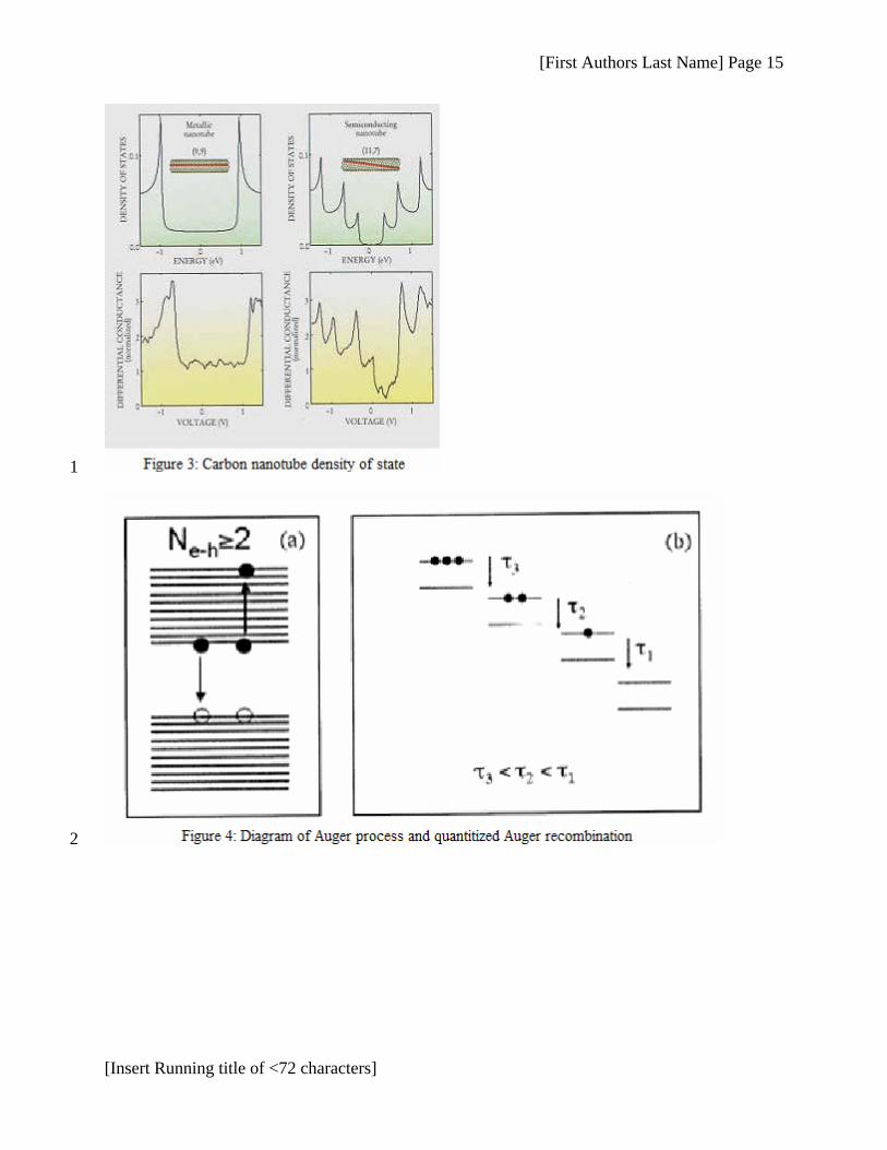
It is obvious that a carbon nanotube is 1D confined material, thus we should expect spikes in the
DOS (density of state) of SWNT due to its 1D nature. Current vs voltage measurement of SWNT
is performed, and the curve is used to characterize the DOS. Figure 3 shows the
experiment result and the corresponding theoretical calculation. One graph shows very good
agreement between the experiment and the theoretical result, but the other one shows some
deviation between the two. Further investigation is needed to resolve this discrepancy; however,
a spike-like 1D DOS is clearly shown here.
dVdI /
Ultra-fast optical spectroscopy of SWNT
Although carbon nanotube has shown excellent mechanical and electrical properties, its optical
properties are still not quite clear, and many important questions for carbon nanotube still remain
unsolved. Among them, the exciton effects on the optical properties are crucial, because excitons
have significant effect on quantum confined material system. In this chapter, excitonic properties
of SWNT are studied through ultra-fast optical spectroscopy. Both auger recombination and
many-body effect of confined excitons are studied, and the possibility of nanotube-based
optoelectronics devices is discussed.
1 Auger recombination of excitons
Auger recombination is the non-radiative recombination of electron-hole pairs, in which the
recombination energy is transferred to a third particle (electron or hole) that is excited to a higher
energy state. Figure 4 shows the schematic diagram of an Auger process. In bulk materials, the
Auger recombination process is suppressed due to the energy and momentum conservation
requirement. However, in reduce dimension systems, especially 0D quantum dot and 1D
quantum wire, the requirement of momentum conservation is relaxed and thus Auger
recombination can be the dominant non-radiative process. Auger recombination in reduced
dimension materials also differs from that of bulk material in the regime of a few excitons per
particle, for which Auger recombination occurs at a sequence of quantized steps from N excitons
to N-1 excitons, and finally to 1 exciton in the particle. In this quantized Auger recombination
picture, Auger recombination rate is characterized by a set of discrete recombination time
constants instead of a continuum of density-dependent recombination time constants as in bulk
materials.
Experiments based on ultra-fast optical spectroscopy have been performed to study the Auger-
like exciton-exciton recombination processes in SWNT. Figure 5 shows the experiment setup
for the pump-probe experiment, the ultra-short laser pulse is used as the pump laser for the
SWNT sample; probe beam at several wavelength passes through the sample which is already
excited by the pump beam. By changing the variable time delay between the pump beam and the
probe beam, transient absorption data were obtained by measurement of the transmission of the
probe beam. Useful information such as Auger recombination life time, population decay
dynamics can be obtained by studying the pump-probe experiment data.
Figure 6 shows a typical pump-probe experiment result. Different curves are measured at
different pump intensity, starting from for lowest curve groups, to 213 /1020,8,4,2 cmphotons×
214 /1020,10,8,5 cmphotons× for middle curve group, and for top
curve group. From the curve, it is easy to extract the Auger recombination lifetime information.
And conclusions are:
215 /105,4.3 cmphotons×
a) Although the pump beam intensity in increased in a continuous way, the transient
absorption curves are clearly clustered into three groups. This grouping behavior shows
the quantized Auger recombination at several excitons per particle levels. In fact, the
number of exciton per SWNT changes in discrete steps from 3, to 2, and finally to 1
exciton; and each step is characterized by a specific Auger recombination lift time.
b) The pump-probe curve shows that the Auger recombination time constant for 2 excitons
and 3 excitons are extremely small, in the range of 2-3 ps. This suggests a very strong
Auger-effect, compared to other quantum confinement systems. For example, Auger
recombination life time for CdSe quantum rods and quantum dots are on the order of tens
of ps or hundreds of ps depending on the numbers of excitons in each particle.
The ultrafast optical spectroscopy results show that Auger recombination process dominates the
e-h pair recombination process, and this process is characterized by a life time in the order of
several ps time scale. This rapid loss of e-h pair due to Auger recombination limits the possibility
of generating population inversion in SWNT, and thus the application of SWNT in
optoelectronics is quite limited. However, research also shows that the engineering of the
dimension of quantum rods can actually slow down the Auger recombination rate at certain
wavelengths. Thus further research may be needed to investigate the optoelectronic application
of SWNT.
2. Blue-shifted exciton resonance
Aside from Auger recombination of excitons, at high exciton concentration, many-body
interactions significantly affect the excitonic properties of semiconductors. Originally, exciton
effects are studied through simple Hydrogen atom model, and exciton energy levels are stable
when the exciton Bohr radius is smaller than the exciton-exciton distance – where this simple
model is still accurate. However, at intense laser excitation level, large amounts of excitons can
be created with in one particle or SWNT, and the confinement of these excitons in one particle
leads to the reduction of exciton distance. At this limit, many-body effects dominate and exciton
energy level is renormalized.
Many-body effects have been exploited in 2D or 3D semiconductor materials, both
experimentally and theoretically. Study shows that with increasing densities of excitons, the
excitonic absorption spectrum can shift, broaden or saturate due to many-body effect. Intuitively,
we should expect a stronger many-body effect on the exciton energy level in 1D SWNT or 0D
quantum dots, because of the exciton spatial confinement. To study this effect, frequency
resolved transient absorption measurement was preformed for SWNT samples, because SWNTs
have smaller tube diameters and thus higher spatial confinement than quantum wires. Thus we
are expecting to see even strong many-body effect for SWNTs.
The experiment setup is the same as in Figure 6; the differential transmission of the probe at
zero delay is plotted in Figure 7 as a function of probe wavelength; the excitation wavelength is
chosen to resonantly excite the low excitonic state of SWNTs; and the excitation intensity is
chosen to be ~ , which corresponding to an excitonic density of ~5 excitons
per SWNT. The “dip” of the transmission spectrum curve is explained by the author photon-
induced absorption; this absorption is only observed in the blue-side of the pump and only at
high excitation intensity level. Time-resolve measurement also shows that this absorption
215 /105 cmphotons×
recovers after ~600 fs, which corresponds to the life time of Auger recombination for 5 excitons
per SWNT. These observations are explained by the blue-shift of excitonic energy level for
multiple excitons confined in a single SWNT, due to many-body effect. And as multiple excitons
quickly recombined due to Auger process within ~1ps, many-body effect disappears and the
transmission of probe signal recovers. However, further investigation for this subject is still
needed to determine the effect of multiple excitons confined with in one SWNT.
Applications
Ever since the discovery of carbon nanotube, the small dimension, strength and unique electronic
band structure of carbon nanotubes make them unique for all kinds of applications. In this part of
the review paper, we describe some of the important applications of carbon nanotubes, especially
the applications in nano-electronics and biological applications. Other potential applications,
such as composite material applications and applications in energy will not be covered here.
1. Biological applications
a) Functional AFM tips
As shown in Figure 8, a typical AFM (atom force microscope) is composed of a cantilever-
tip assembly; a laser that shines laser beam onto the cavalier; and a detector to monitor
cantilever displacement through the displacement of reflected laser beam. Clearly, from the
figure we can see that the resolution of the AFM will be highly dependent on the nature of
the cantilever-tip, such as the size, stiffness and curvature at the tip. In fact, it is proposed
that for an ideal AFM tip, it should have a high aspect ratio, the tip radius should be as small
as possible, and it should be mechanically and chemically robust so that its structure is not
changed when imaging in fluid environments. And in fact, carbon nanotube seems to be the
only candidate to satisfy all the requirements mentioned above because of its superior
mechanical and chemical properties. In this part of this review paper, carbon nanotube as
functional AFM tips for biological applications will be discussed.
First, Carbon nanotubes are attached to silicon tip through manual assembly or by direct
growth through CVD. And it is shown that, the direct growth method provides the possibility
of mass production, and thin, individual SWNTs tips that are difficult to achieve through
other methods.
Research reports by Lieber group have shown that, CVD nanotube tips for structural imaging
have been used in structural biology to image aggregation pathway of amyloid proteins, to
address ATP-dependent nucleosome remodeling, and for DNA sequence determination.
However, it is also possible to utilize the high sensitivity of AFM to normal forces for
biological and chemical sensitive measurement. In fact, the AFM tip is simply modified with
specific chemical groups, and the force between the chemical group and the sample can be
measured at the same time as the surface topography. Once again, carbon nanotube tips are
proven to be the perfect candidate for this kind of application. They have small radius of
curvature at the tip, and the tip can be specially modified only at the ends. Research work
already shows that modified SWNT could lead to sub-nm resolution in chemical bonding site
recognitions.
b) Bio-sensing based applications
In traditional electrochemiluminescence (ECL), a label is first excited to higher energy state
by electron transfer reactions near the surface of an electrode. And a photon is emitted when
the label relaxed to the ground state. For biosensing applications, an ECL label is coupled to
an analyte of interest and then excited to higher energy state. Since the number of photons
emitted in this process scales with the number of excited labels, it is possible to quantitatively
measure the concentration of analyte that is of interest.
It is already shown that carbon nanotubes have several characteristics that make them useful
for ECL-based biosensing applications. First, carbon nanotubes are conducting, thus it can
act as electrode and generate ECL in liquid solution. Secondly, carbon nanotubes can be
derivatized with functional groups that allow immobilization of biomolecules. And thirdly,
carbon nanotubes have high surface area to weight ratio, and most of the surface areas can be
utilized for ECL and immobilization of biomolecules. In fact, carbon nanotubes based ECL
biosensing systems have already been fabricated, and they have the ability to quantitatively
measure a wide range of biological analytes.
2. Electrical applications
a) Field emission device
As we all know, nanotubes are the best field emitters among all the material because of their
high electrical conductivity, and the insuperable sharpness of their tip which also means that
they emit at especially low voltage, the most important feature for building electrical devices
that utilize this feature. Nanotubes can carry an amazingly high current density, possibly as
high as 1013 A/cm2 .What is even more, the current is extremely stable according to the
latest research.
A direct application of this feature of nanotubes is in field-emission flat-panel displays. What
is filed emission? Field emission is emission of electrons from the surface of a condensed
phase into another phase usually vacuum, under the action of a high electrostatic field (108
V/cm). It is a quantum effect. Instead of a single electron gun, here there is a separate
electron gun (or many) for each pixel in the display, which has high current density, low
turn-on and operating voltage, and steady, long-lived behavior. Figure 9 shows the diagram
of carbon nanotube based field emission devices.
b) Molecular electronics
In any electronic circuit, especially the ones in microelectronic level, the interconnections
between switches and other active devices become increasingly important. As the result of
wonderful geometry, electrical conductivity, and ability to be precisely derived, Nanotubes
become the ideal candidates for the connections in molecular electronics. Moreover, they
have been demonstrated as switches themselves. The reason is that nanotubes conductivity is
determined by surrounding environments. In different environment, it can present as
conductor, semiconductor and insulator respectively. That is to say, we can easily control the
conductivity of nanotubes via changing the conditions nanotubues face. Based on this
feature, we can easily adjust the whole characteristics of the circuits without adding any other
electronic devices. At the present time, nanotubes have been widely used in microelectronics.
Figure 10 shows the picture of a carbon nanotube based molecular device.
3 Energy applications
Recent research has shown that nanotubes contain the highest reversible capacity of any
carbon material for use in lithium-ion batteries. Nanotubes also have applications in a variety
of fuel cell components. They have a number of properties including high surface area and
thermal conductivity that make them useful as electrode catalyst supports in PEM fuel cells.
Nanotubes' high strength and toughness to weight characteristics may also prove valuable as
part of composite components in fuel cells that are deployed in transport applications where
durability is extremely important.
Conclusion
Ever since carbon nanotube was found in 1991, it has attracted much attention because of its
excellent mechanical and electrical properties. Although ultrafast optical spectroscopy of carbon
nanotube shows that its optoelectronic applications are limited due to Auger recombination,
carbon nanotube is still quite promising in nano-electronics, biological applications and
composite material applications. The method for industrial mass production of high quality
carbon nanotube is still missing, thus the application for carbon nanotube is still in its childhood.
However, carbon nanotube will have a bright future in the emerging nano-technology age.