SMSC CAP1188 DATASHEET Revision 1.32 (01-05-12) Datasheet PRODUCT FEATURES CAP1188 8 Channel Capacitive Touch Sensor with 8 LED Drivers General Description The CAP1188, which incorporates SMSC’s RightTouch ® 1 technology, is a multiple channel Capacitive Touch sensor with multiple power LED drivers. It contains eight (8) individual capacitive touch sensor inputs with programmable sensitivity for use in touch sensor applications. Each sensor input automatically recalibrates to compensate for gradual environmental changes. The CAP1188 also contains eight (8) LED drivers that offer full-on / off, variable rate blinking, dimness controls, and breathing. Each of the LED drivers may be linked to one of the sensor inputs to be actuated when a touch is detected. As well, each LED driver may be individually controlled via a host controller. The CAP1188 includes Multiple Pattern Touch recognition that allows the user to select a specific set of buttons to be touched simultaneously. If this pattern is detected, then a status bit is set and an interrupt generated. Additionally, the CAP1188 includes circuitry and support for enhanced sensor proximity detection. The CAP1188 offers multiple power states operating at low quiescent currents. In the Standby state of operation, one or more capacitive touch sensor inputs are active and all LEDs may be used. If a touch is detected, it will wake the system using the WAKE/SPI_MOSI pin. Deep Sleep is the lowest power state available, drawing 5uA (typical) of current. In this state, no sensor inputs are active. Driving the WAKE/SPI_MOSI pin or communications will wake the device. Applications Desktop and Notebook PCs LCD Monitors Consumer Electronics Appliances Features Eight (8) Capacitive Touch Sensor Inputs — Programmable sensitivity — Automatic recalibration — Individual thresholds for each button Proximity Detection Multiple Button Pattern Detection Calibrates for Parasitic Capacitance Analog Filtering for System Noise Sources Press and Hold feature for Volume-like Applications Multiple Communication Interfaces — SMBus / I 2 C compliant interface — SMSC BC-Link interface — SPI communications — Pin selectable communications protocol and multiple slave addresses (SMBus / I 2 C only) Low Power Operation — 5uA quiescent current in Deep Sleep — 50uA quiescent current in Standby (1 sensor input monitored) — Samples one or more channels in Standby Eight (8) LED Driver Outputs — Open Drain or Push-Pull — Programmable blink, breathe, and dimness controls — Can be linked to Capacitive Touch Sensor inputs Dedicated Wake output flags touches in low power state System RESET pin Available in 24-pin 4mm x 4mm RoHS compliant QFN package Block Diagram 1. SMSC, the SMSC logo and RightTouch are registered trademarks and the RightTouch logo is a trademark of Standard Microsystems Corporation (“SMSC”). SMBus / BC-Link or SPI Slave Protocol SMCLK / BC_CLK / SPI_CLK SMDATA / BC_DATA / SPI_MSIO / SPI_MISO VDD ALERT# / BC_IRQ# Capacitive Touch Sensing Algorithm LED1 CS1 CS2 CS3 CS4 CS5 CS6 LED Driver, Breathe, and Dimness control WAKE / SPI_MOSI CS7 CS8 RESET ADDR_COMM SPI_CS# LED2 LED3 LED4 LED5 LED6 LED7 LED8 GND
Transcript
CAP1188
8 Channel Capacitive Touch Sensor with 8 LED Drivers
DatasheetPRODUCT FEATURESGeneral DescriptionThe CAP1188, which incorporates SMSC’s RightTouch® 1
technology, is a multiple channel Capacitive Touch sensorwith multiple power LED drivers. It contains eight (8)ind iv idua l capac i t i ve touch sensor inpu ts w i thprogrammable sensit ivity for use in touch sensorapplications. Each sensor input automatically recalibratesto compensate for gradual environmental changes.The CAP1188 also contains eight (8) LED drivers that offerfull-on / off, variable rate blinking, dimness controls, andbreathing. Each of the LED drivers may be linked to one ofthe sensor inputs to be actuated when a touch is detected.As well, each LED driver may be individually controlled viaa host controller.The CAP1188 includes Multiple Pattern Touch recognitionthat allows the user to select a specific set of buttons to betouched simultaneously. If this pattern is detected, then astatus bit is set and an interrupt generated.Additionally, the CAP1188 includes circuitry and support forenhanced sensor proximity detection. The CAP1188 offers multiple power states operating at lowquiescent currents. In the Standby state of operation, oneor more capacitive touch sensor inputs are active and allLEDs may be used. If a touch is detected, it will wake thesystem using the WAKE/SPI_MOSI pin.Deep Sleep is the lowest power state available, drawing5uA (typical) of current. In this state, no sensor inputs areactive. Driving the WAKE/SPI_MOSI pin or communicationswill wake the device.
ApplicationsDesktop and Notebook PCsLCD MonitorsConsumer ElectronicsAppliances
FeaturesEight (8) Capacitive Touch Sensor Inputs— Programmable sensitivity— Automatic recalibration — Individual thresholds for each buttonProximity DetectionMultiple Button Pattern DetectionCalibrates for Parasitic CapacitanceAnalog Filtering for System Noise SourcesPress and Hold feature for Volume-like ApplicationsMultiple Communication Interfaces— SMBus / I2C compliant interface— SMSC BC-Link interface— SPI communications— Pin selectable communications protocol and multiple
slave addresses (SMBus / I2C only)Low Power Operation— 5uA quiescent current in Deep Sleep— 50uA quiescent current in Standby (1 sensor input
monitored)— Samples one or more channels in StandbyEight (8) LED Driver Outputs— Open Drain or Push-Pull — Programmable blink, breathe, and dimness controls— Can be linked to Capacitive Touch Sensor inputsDedicated Wake output flags touches in low power state System RESET pin Available in 24-pin 4mm x 4mm RoHS compliant QFN package
Block Diagram
1. SMSC, the SMSC logo and RightTouch are registered trademarksand the RightTouch logo is a trademark of Standard MicrosystemsCorporation (“SMSC”).
8 Channel Capacitive Touch Sensor with 8 LED Drivers
Datasheet
Revisio
CopyrightCircuit diaconstructreserves before plarights or version oknown asdesigneddamage. this docutrademarkThe Micro
SMSC DIFITNESSOF DEALDAMAGETORT; NETO HAVE
Ordering Information:
Reel size is 4,000 piecesThis product meets the halogen maximum concentration values per IEC61249-2-21
For RoHS compliance and environmental information, please visit www.smsc.com/rohs
Please contact your SMSC sales representative for additional documentation related to this product such as application notes, anomaly sheets, and design guidelines.
ORDERING NUMBER PACKAGE FEATURES
AP1188-1-CP-TR 24-pin QFN 4mm x 4mm(Lead-free RoHS compliant)
ion purposes is not necessarily given. Although the information has been checked and is believed to be accurate, no responsibility is assumed for inaccuracies. SMSCthe right to make changes to specifications and product descriptions at any time without notice. Contact your local SMSC sales office to obtain the latest specificationscing your product order. The provision of this information does not convey to the purchaser of the described semiconductor devices any licenses under any patent
other intellectual property rights of SMSC or others. All sales are expressly conditional on your agreement to the terms and conditions of the most recently datedf SMSC's standard Terms of Sale Agreement dated before the date of your order (the "Terms of Sale Agreement"). The product may contain design defects or errors anomalies which may cause the product's functions to deviate from published specifications. Anomaly sheets are available upon request. SMSC products are not, intended, authorized or warranted for use in any life support or other application where product failure could cause or contribute to personal injury or severe propertyAny and all such uses without prior written approval of an Officer of SMSC and further testing and/or modification will be fully at the risk of the customer. Copies ofment or other SMSC literature, as well as the Terms of Sale Agreement, may be obtained by visiting SMSC’s website at http://www.smsc.com. SMSC is a registered of Standard Microsystems Corporation (“SMSC”). Product names and company names are the trademarks of their respective holders. chip name and logo, and the Microchip logo are registered trademarks of Microchip Technology Incorporated in the U.S.A. and other countries.
SCLAIMS AND EXCLUDES ANY AND ALL WARRANTIES, INCLUDING WITHOUT LIMITATION ANY AND ALL IMPLIED WARRANTIES OF MERCHANTABILITY, FOR A PARTICULAR PURPOSE, TITLE, AND AGAINST INFRINGEMENT AND THE LIKE, AND ANY AND ALL WARRANTIES ARISING FROM ANY COURSEING OR USAGE OF TRADE. IN NO EVENT SHALL SMSC BE LIABLE FOR ANY DIRECT, INCIDENTAL, INDIRECT, SPECIAL, PUNITIVE, OR CONSEQUENTIALS; OR FOR LOST DATA, PROFITS, SAVINGS OR REVENUES OF ANY KIND; REGARDLESS OF THE FORM OF ACTION, WHETHER BASED ON CONTRACT;GLIGENCE OF SMSC OR OTHERS; STRICT LIABILITY; BREACH OF WARRANTY; OR OTHERWISE; WHETHER OR NOT ANY REMEDY OF BUYER IS HELD FAILED OF ITS ESSENTIAL PURPOSE, AND WHETHER OR NOT SMSC HAS BEEN ADVISED OF THE POSSIBILITY OF SUCH DAMAGES.
Open drain LED 1 driver (default) OD (5V) Connect to Ground
Push-pull LED 1 driver DO leave open or
connect to Ground
6 LED2
Open drain LED 2 driver (default) OD (5V) Connect to Ground
Push-pull LED 2 driver DO leave open or
connect to Ground
7 LED3
Open drain LED 3 driver (default) OD (5V) Connect to Ground
Push-pull LED 3 driver DO leave open or
connect to Ground
8 LED4
Open drain LED 4 driver (default) OD (5V) Connect to Ground
Push-pull LED 4 driver DO leave open or
connect to Ground
9 LED5
Open drain LED 5 driver (default) OD (5V) Connect to Ground
Push-pull LED 5 driver DO leave open or
connect to Ground
10 LED6
Open drain LED 6 driver (default) OD (5V) Connect to Ground
Push-pull LED 6 driver DO leave open or
connect to Ground
Table 1.1 Pin Description for CAP1188 (continued)
PIN # PIN NAME PIN FUNCTION PIN TYPEUNUSED
CONNECTION
Revision 1.32 (01-05-12) 10 SMSC CAP1188DATASHEET
8 Channel Capacitive Touch Sensor with 8 LED Drivers
Datasheet
APPLICATION NOTE: When the ALERT# pin is configured as an active low output, it will be open drain. When itis configured as an active high output, it will be push-pull.
11 LED7
Open drain LED 7 driver (default) OD (5V) Connect to Ground
Push-pull LED 7 driver DO leave open or
connect to Ground
12 LED8
Open drain LED 8 driver (default) OD (5V) Connect to Ground
Push-pull LED 8 driver DO leave open or
connect to Ground
13 ALERT# / BC_IRQ#
ALERT# - Active low alert / interrupt output for SMBus alert or SPI interrupt - requires pull-up
resistor (default)OD (5V) Connect to
Ground
ALERT - Active high push-pull alert / interrupt output for SMBus alert or SPI interrupt DO leave open
BC_IRQ# - Active low interrupt / optional for BC-Link - requires pull-up resistor OD (5V) Connect to
Ground
BC_IRQ - Active high push-pull interrupt / optional for BC-Link DO leave open
24 RESET Active high soft reset for system - resets all registers to default values. DI (5V) Connect to GND
Bottom Pad GND Ground Power n/a
Table 1.1 Pin Description for CAP1188 (continued)
PIN # PIN NAME PIN FUNCTION PIN TYPEUNUSED
CONNECTION
SMSC CAP1188 11 Revision 1.32 (01-05-12)DATASHEET
8 Channel Capacitive Touch Sensor with 8 LED Drivers
Datasheet
APPLICATION NOTE: For the 5V tolerant pins that have a pull-up resistor, the pull-up voltage must not exceed 3.6Vwhen the CAP1188 is unpowered.
APPLICATION NOTE: The SPI_CS# pin should be grounded when SMBus, I2C, or BC-Link communications areused.
The pin types are described in Table 1.2. All pins labeled with (5V) are 5V tolerant.
Table 1.2 Pin Types
PIN TYPE DESCRIPTION
Power This pin is used to supply power or ground to the device.
DI Digital Input - This pin is used as a digital input. This pin is 5V tolerant.
AIO Analog Input / Output -This pin is used as an I/O for analog signals.
DIOD Digital Input / Open Drain Output - This pin is used as a digital I/O. When it is used as an output, it is open drain and requires a pull-up resistor. This pin is 5V tolerant.
OD Open Drain Digital Output - This pin is used as a digital output. It is open drain and requires a pull-up resistor. This pin is 5V tolerant.
DO Push-pull Digital Output - This pin is used as a digital output and can sink and source current.
DIO Push-pull Digital Input / Output - This pin is used as an I/O for digital signals.
Revision 1.32 (01-05-12) 12 SMSC CAP1188DATASHEET
8 Channel Capacitive Touch Sensor with 8 LED Drivers
Datasheet
Chapter 2 Electrical Specifications
Note 2.1 Stresses above those listed could cause permanent damage to the device. This is a stressrating only and functional operation of the device at any other condition above thoseindicated in the operation sections of this specification is not implied.
Note 2.2 For the 5V tolerant pins that have a pull-up resistor, the voltage difference betweenV5VT_PIN and VDD must never exceed 3.6V.
Note 2.3 The Package Power Dissipation specification assumes a recommended thermal via designconsisting of a 3x3 matrix of 0.3mm (12mil) vias at 1.0mm pitch connected to the groundplane with a 2.5 x 2.5mm thermal landing.
Note 2.4 Junction to Ambient (θJA) is dependent on the design of the thermal vias. Without thermalvias and a thermal landing, the θJA is approximately 60°C/W including localized PCBtemperature increase.
Table 2.1 Absolute Maximum Ratings
Voltage on 5V tolerant pins (V5VT_PIN) -0.3 to 5.5 V
Voltage on 5V tolerant pins (|V5VT_PIN - VDD|) Note 2.2 0 to 3.6 V
Voltage on VDD pin -0.3 to 4 V
Voltage on any other pin to GND -0.3 to VDD + 0.3 V
Package Power Dissipation up to TA = 85°C for 24 pin QFN(see Note 2.3)
0.9 W
Junction to Ambient (θJA) (see Note 2.4) 58 °C/W
Operating Ambient Temperature Range -40 to 125 °C
Storage Temperature Range -55 to 150 °C
ESD Rating, All Pins, HBM 8000 V
Table 2.2 Electrical Specifications
VDD = 3V to 3.6V, TA = 0°C to 85°C, all Typical values at TA = 27°C unless otherwise noted.
CHARACTERISTIC SYMBOL MIN TYP MAX UNIT CONDITIONS
DC Power
Supply Voltage VDD 3.0 3.3 3.6 V
SMSC CAP1188 13 Revision 1.32 (01-05-12)DATASHEET
8 Channel Capacitive Touch Sensor with 8 LED Drivers
Datasheet
Supply Current
ISTBY 120 170 uA
Standby state active 1 sensor input monitored
No LEDs activeDefault conditions (8 avg, 70ms
cycle time)
ISTBY 50 uA
Standby state active1 sensor input monitored
No LEDs active1 avg, 140ms cycle time,
IDSLEEP 5 15 uA
Deep Sleep state activeLEDs at 100% or 0% Duty Cycle
No communicationsTA < 40°C
3.135 < VDD < 3.465V
IDD 500 600 uA Capacitive Sensing ActiveNo LEDs active
Capacitive Touch Sensor Inputs
Maximum Base Capacitance CBASE 50 pF Pad untouched
Minimum Detectable Capacitive Shift ΔCTOUCH 20 fF
Pad touched - default conditions (1 avg, 35ms cycle time, 1x
sensitivity)
Recommended Cap Shift ΔCTOUCH 0.1 2 pF Pad touched - Not tested
Power Supply Rejection PSR ±3 ±10 counts
/ V
Untouched Current Counts Base Capacitance 5pF - 50pF
Maximum sensitivityNegative Delta Counts disabled
All other parameters default
Timing
RESET Pin Delay tRST_DLY 10 ms
Time to communications
readytCOMM_DLY 15 ms
Time to first conversion ready tCONV_DLY 170 200 ms
LED Drivers
Duty Cycle DUTYLED 0 100 % Programmable
Drive Frequency fLED 2 kHz
Sinking Current ISINK 24 mA VOL = 0.4
Sourcing Current ISOURCE 24 mA VOH = VDD - 0.4
Table 2.2 Electrical Specifications (continued)
VDD = 3V to 3.6V, TA = 0°C to 85°C, all Typical values at TA = 27°C unless otherwise noted.
CHARACTERISTIC SYMBOL MIN TYP MAX UNIT CONDITIONS
Revision 1.32 (01-05-12) 14 SMSC CAP1188DATASHEET
8 Channel Capacitive Touch Sensor with 8 LED Drivers
Datasheet
Leakage Current ILEAK ±5 uA
powered or unpoweredTA < 85°C
pull-up voltage < 3.6V if unpowered
I/O Pins
Output Low Voltage VOL 0.4 V ISINK_IO = 8mA
Output High Voltage VOHVDD -
0.4 V ISOURCE_IO = 8mA
Input High Voltage VIH 2.0 V
Input Low Voltage VIL 0.8 V
Leakage Current ILEAK ±5 uA
powered or unpoweredTA < 85°C
pull-up voltage < 3.6V if unpowered
RESET Pin Release to conversion ready tRESET 170 200 ms
SMBus Timing
Input Capacitance CIN 5 pF
Clock Frequency fSMB 10 400 kHz
Spike Suppression tSP 50 ns
Bus Free Time Stop to Start tBUF 1.3 us
Start Setup Time tSU:STA 0.6 us
Start Hold Time tHD:STA 0.6 us
Stop Setup Time tSU:STO 0.6 us
Data Hold Time tHD:DAT 0 us When transmitting to the master
Data Hold Time tHD:DAT 0.3 us When receiving from the master
Data Setup Time tSU:DAT 0.6 us
Clock Low Period tLOW 1.3 us
Clock High Period tHIGH 0.6 us
Clock / Data Fall Time tFALL 300 ns Min = 20+0.1CLOAD ns
Clock / Data Rise Time tRISE 300 ns Min = 20+0.1CLOAD ns
Capacitive Load CLOAD 400 pF per bus line
Table 2.2 Electrical Specifications (continued)
VDD = 3V to 3.6V, TA = 0°C to 85°C, all Typical values at TA = 27°C unless otherwise noted.
CHARACTERISTIC SYMBOL MIN TYP MAX UNIT CONDITIONS
SMSC CAP1188 15 Revision 1.32 (01-05-12)DATASHEET
8 Channel Capacitive Touch Sensor with 8 LED Drivers
Datasheet
Note 2.5 The ALERT pin will not glitch high or low at power up if connected to VDD or anothervoltage.
Note 2.6 The SMCLK and SMDATA pins will not glitch low at power up if connected to VDD oranother voltage.
BC-Link Timing
Clock Period tCLK 250 ns
Data Hold Time tHD:DAT 0 ns
Data Setup Time tSU:DAT 30 ns Data must be valid before clock
Clock Duty Cycle Duty 40 50 60 %
SPI Timing
Clock Period tP 250 ns
Clock Low Period tLOW 0.4 x tP 0.6 x tP ns
Clock High Period tHIGH 0.4 x tP 0.6 x tP ns
Clock Rise / Fall time
tRISE / tFALL
0.1 x tP ns
Data Output Delay tD:CLK 10 ns
Data Setup Time tSU:DAT 20 ns
Data Hold Time tHD:DAT 20 ns
SPI_CS# to SPI_CLK setup time tSU:CS 0 ns
Wake Time tWAKE 10 20 us SPI_CS# asserted to CLK assert
Table 2.2 Electrical Specifications (continued)
VDD = 3V to 3.6V, TA = 0°C to 85°C, all Typical values at TA = 27°C unless otherwise noted.
CHARACTERISTIC SYMBOL MIN TYP MAX UNIT CONDITIONS
Revision 1.32 (01-05-12) 16 SMSC CAP1188DATASHEET
8 Channel Capacitive Touch Sensor with 8 LED Drivers
Datasheet
Chapter 3 Communications
3.1 CommunicationsThe CAP1188 communicates using the 2-wire SMBus or I2C bus, the 2-wire proprietary BC-Link, orthe SPI bus. Regardless of communication mechanism, the device functionality remains unchanged.The communications mechanism as well as the SMBus (or I2C) slave address is determined by theresistor connected between the ADDR_COMM pin and ground as shown in Table 3.1.
3.1.1 SMBus (I2C) Communications
When configured to communicate via the SMBus, the CAP1188 supports the following protocols: SendByte, Receive Byte, Read Byte, Write Byte, Read Block, and Write Block. In addition, the devicesupports I2C formatting for block read and block write protocols.
APPLICATION NOTE: For SMBus/I2C communications, the SPI_CS# pin is not used and should be grounded; anydata presented to this pin will be ignored.
See Section 3.2 and Section 3.3 for more information on the SMBus bus and protocols respectively.
3.1.2 SPI Communications
When configured to communicate via the SPI bus, the CAP1188 supports both bi-directional 3-wireand normal 4-wire protocols and uses the SPI_CS# pin to enable communications.
See Section 3.5 and Section 3.6 for more information on the SPI bus and protocols respectively.
3.1.3 BC-Link Communications
When BC-Link communications are used, the CAP1188 supports the read byte protocol and the writebyte protocol.
APPLICATION NOTE: For BC-Link communications, the SPI_CS# pin is not used and should be grounded; anydata presented to this pin will be ignored.
Table 3.1 ADDR_COMM Pin Decode
PULL-DOWN RESISTOR (+/- 5%) PROTOCOL USED SMBUS ADDRESS
GND SPI Communications using Normal 4-wire Protocol Used n/a
56k SPI Communications using Bi-Directional 3-wire Protocol Used n/a
68k BC-Link Communications n/a
82k SMBus / I2C 0101_100(r/w)
100k SMBus / I2C 0101_011(r/w)
120k SMBus / I2C 0101_010(r/w)
150k SMBus / I2C 0101_001(r/w)
VDD SMBus / I2C 0101_000(r/w)
SMSC CAP1188 17 Revision 1.32 (01-05-12)DATASHEET
8 Channel Capacitive Touch Sensor with 8 LED Drivers
Datasheet
See Section 3.8 for more information on the BC-Link Bus and protocols respectively.
APPLICATION NOTE: Upon power up, the CAP1188 will not respond to any communications for up to 15ms. Afterthis time, full functionality is available.
3.2 System Management BusThe CAP1188 communicates with a host controller, such as an SMSC SIO, through the SMBus. TheSMBus is a two-wire serial communication protocol between a computer host and its peripheraldevices. A detailed timing diagram is shown in Figure 3.1. Stretching of the SMCLK signal is supported;however, the CAP1188 will not stretch the clock signal.
3.2.1 SMBus Start Bit
The SMBus Start bit is defined as a transition of the SMBus Data line from a logic ‘1’ state to a logic‘0’ state while the SMBus Clock line is in a logic ‘1’ state.
3.2.2 SMBus Address and RD / WR Bit
The SMBus Address Byte consists of the 7-bit client address followed by the RD / WR indicator bit. Ifthis RD / WR bit is a logic ‘0’, then the SMBus Host is writing data to the client device. If this RD / WRbit is a logic ‘1’, then the SMBus Host is reading data from the client device.
See Table 3.1 for available SMBus addresses.
3.2.3 SMBus Data Bytes
All SMBus Data bytes are sent most significant bit first and composed of 8-bits of information.
3.2.4 SMBus ACK and NACK Bits
The SMBus client will acknowledge all data bytes that it receives. This is done by the client devicepulling the SMBus Data line low after the 8th bit of each byte that is transmitted. This applies to boththe Write Byte and Block Write protocols.
The Host will NACK (not acknowledge) the last data byte to be received from the client by holding theSMBus data line high after the 8th data bit has been sent. For the Block Read protocol, the Host willACK each data byte that it receives except the last data byte.
Figure 3.1 SMBus Timing Diagram
SMDATA
SMCLK
TLOW
TRISE
THIGH
TFALL
TBUF
THD:STA
P S S - Start Condition P - Stop Condition
THD:DAT TSU:DATTSU:STA
THD:STA
P
TSU:STO
S
Revision 1.32 (01-05-12) 18 SMSC CAP1188DATASHEET
8 Channel Capacitive Touch Sensor with 8 LED Drivers
Datasheet
3.2.5 SMBus Stop Bit
The SMBus Stop bit is defined as a transition of the SMBus Data line from a logic ‘0’ state to a logic‘1’ state while the SMBus clock line is in a logic ‘1’ state. When the CAP1188 detects an SMBus Stopbit and it has been communicating with the SMBus protocol, it will reset its client interface and prepareto receive further communications.
3.2.6 SMBus Timeout
The CAP1188 includes an SMBus timeout feature. Following a 30ms period of inactivity on the SMBuswhere the SMCLK pin is held low, the device will timeout and reset the SMBus interface.
The timeout function defaults to disabled. It can be enabled by setting the TIMEOUT bit in theConfiguration register (see Section 5.6, "Configuration Registers").
3.2.7 SMBus and I2C Compatibility
The major differences between SMBus and I2C devices are highlighted here. For more information,refer to the SMBus 2.0 and I2C specifications. For information on using the CAP1188 in an I2C system,refer to SMSC AN 14.0 SMSC Dedicated Slave Devices in I2C Systems.
1. CAP1188 supports I2C fast mode at 400kHz. This covers the SMBus max time of 100kHz.
2. Minimum frequency for SMBus communications is 10kHz.
3. The SMBus client protocol will reset if the clock is held at a logic ‘0’ for longer than 30ms. Thistimeout functionality is disabled by default in the CAP1188 and can be enabled by writing to theTIMEOUT bit. I2C does not have a timeout.
4. The SMBus client protocol will reset if both the clock and data lines are held at a logic ‘1’ for longerthan 200µs (idle condition). This function is disabled by default in the CAP1188 and can be enabledby writing to the TIMEOUT bit. I2C does not have an idle condition.
5. I2C devices do not support the Alert Response Address functionality (which is optional for SMBus).
6. I2C devices support block read and write differently. I2C protocol allows for unlimited number ofbytes to be sent in either direction. The SMBus protocol requires that an additional data byteindicating number of bytes to read / write is transmitted. The CAP1188 supports I2C formatting only.
3.3 SMBus Protocols The CAP1188 is SMBus 2.0 compatible and supports Write Byte, Read Byte, Send Byte, and ReceiveByte as valid protocols as shown below.
All of the below protocols use the convention in Table 3.2.
Table 3.2 Protocol Format
DATA SENT TO DEVICE
DATA SENT TO THE HOST
Data sent Data sent
SMSC CAP1188 19 Revision 1.32 (01-05-12)DATASHEET
8 Channel Capacitive Touch Sensor with 8 LED Drivers
Datasheet
ST P
1-> 1
3.3.1 SMBus Write Byte
The Write Byte is used to write one byte of data to a specific register as shown in Table 3.3.
3.3.2 SMBus Read Byte
The Read Byte protocol is used to read one byte of data from the registers as shown in Table 3.4.
3.3.3 SMBus Send Byte
The Send Byte protocol is used to set the internal address register pointer to the correct addresslocation. No data is transferred during the Send Byte protocol as shown in Table 3.5.
APPLICATION NOTE: The Send Byte protocol is not functional in Deep Sleep (i.e., DSLEEP bit is set).
3.3.4 SMBus Receive Byte
The Receive Byte protocol is used to read data from a register when the internal register addresspointer is known to be at the right location (e.g., set via Send Byte). This is used for consecutive readsof the same register as shown in Table 3.6.
APPLICATION NOTE: The Receive Byte protocol is not functional in Deep Sleep (i.e., DSLEEP bit is set).
The protocols listed below use the convention in Table 3.2.
3.4.1 Block Write
The Block Write is used to write multiple data bytes to a group of contiguous registers as shown inTable 3.7.
APPLICATION NOTE: When using the Block Write protocol, the internal address pointer will be automaticallyincremented after every data byte is received. It will wrap from FFh to 00h.
3.4.2 Block Read
The Block Read is used to read multiple data bytes from a group of contiguous registers as shown inTable 3.8.
APPLICATION NOTE: When using the Block Read protocol, the internal address pointer will be automaticallyincremented after every data byte is received. It will wrap from FFh to 00h.
3.5 SPI Interface The SMBus has a predefined packet structure, the SPI does not. The SPI Bus can operate in twomodes of operation, normal 4-wire mode and bi-directional 3-wire mode. All SPI commands consist of8-bit packets sent to a specific slave device (identified by the CS pin).
The SPI bus will latch data on the rising edge of the clock and the clock and data both idle high.
All commands are supported via both operating modes. The supported commands are: Reset Serialinterface, set address pointer, write command and read command. Note that all other codes receivedduring the command phase are ignored and have no effect on the operation of the device.
Table 3.7 Block Write Protocol
STARTSLAVE
ADDRESS WR ACKREGISTER ADDRESS ACK
REGISTER DATA ACK
1 ->0 YYYY_YYY 0 0 XXh 0 XXh 0
REGISTER DATA ACK
REGISTER DATA ACK . . .
REGISTER DATA ACK STOP
XXh 0 XXh 0 . . . XXh 0 0 -> 1
Table 3.8 Block Read Protocol
SLAVE ADDRESS
WR ACK REGISTER ADDRESS
ACK START SLAVE ADDRESS
RD ACK R
YYY_YYY 0 0 XXh 0 1 ->0 YYYY_YYY 1 0
REGISTER DATA
ACK REGISTER DATA
ACK REGISTER DATA
ACK . . . REGISTER DATA
NACK
XXh 0 XXh 0 XXh 0 . . . XXh 1
SMSC CAP1188 21 Revision 1.32 (01-05-12)DATASHEET
8 Channel Capacitive Touch Sensor with 8 LED Drivers
Datasheet
3.5.1 SPI Normal Mode
The SPI Bus can operate in two modes of operation, normal and bi-directional mode. In the normalmode of operation, there are dedicated input and output data lines. The host communicates by sendinga command along the CAP1188 SPI_MOSI data line and reading data on the SPI_MISO data line.Both communications occur simultaneously which allows for larger throughput of data transactions.
All basic transfers consist of two 8 bit transactions from the Master device while the slave device issimultaneously sending data at the current address pointer value.
Data writes consist of two or more 8-bit transactions. The host sends a specific write commandfollowed by the data to write the address pointer. Data reads consist of one or more 8-bit transactions.The host sends the specific read data command and continues clocking for as many data bytes as itwishes to receive.
3.5.2 SPI Bi-Directional Mode
In the bi-directional mode of operation, the SPI data signals are combined into the SPI_MSIO line,which is shared for data received by the device and transmitted by the device. The protocol uses asimple handshake and turn around sequence for data communications based on the number of clockstransmitted during each phase.
All basic transfers consist of two 8 bit transactions. The first is an 8 bit command phase driven by theMaster device. The second is by an 8 bit data phase driven by the Master for writes, and by theCAP1188 for read operations.
The auto increment feature of the address pointer allows for successive reads or writes. The addresspointer will return to 00h after reaching FFh.
3.5.3 SPI_CS# Pin
The SPI Bus is a single master, multiple slave serial bus. Each slave has a dedicated CS pin (chipselect) that the master asserts low to identify that the slave is being addressed. There are no formaladdressing options.
Figure 3.2 SPI Timing
SPI_MSIO or SPI_MOSI or SPI_MISO
SPI_CLK
tLOW
tRISE
tHIGH
tFALL
tD:CLK tHD:DAT
tSU:DAT
tP
Revision 1.32 (01-05-12) 22 SMSC CAP1188DATASHEET
8 Channel Capacitive Touch Sensor with 8 LED Drivers
Datasheet
3.5.4 Address Pointer
All data writes and reads are accessed from the current address pointer. In both Bi-directional modeand Full Duplex mode, the Address pointer is automatically incremented following every readcommand or every write command.
The address pointer will return to 00h after reaching FFh.
3.5.5 SPI Timeout
The CAP1188 does not detect any timeout conditions on the SPI bus.
3.6 Normal SPI ProtocolsWhen operating in normal mode, the SPI bus internal address pointer is incremented depending uponwhich command has been transmitted. Multiple commands may be transmitted sequentually so longas the SPI_CS# pin is asserted low. Figure 3.3 shows an example of this operation.
SMSC CAP1188 23 Revision 1.32 (01-05-12)DATASHEET
8 Channel C
apacitive Touch Sensor w
ith 8 LED
Drivers
Datasheet
Revision 1.32 (01-05-12)
24 SM
SC
CA
P1188
DATA
SH
EE
T 3
ase of the transaction - command or data,ns are not affected by the reset operation.
Resets the Serial interface whenever two successive 7Ah codes are received. Regardless of the current phthe receipt of the successive reset commands resets the Serial communication interface only. All other functio
Figure 3.3 Example SPI Bus Communication - Normal Mode
8 Channel Capacitive Touch Sensor with 8 LED Drivers
Datasheet
3.6.2 Set Address Pointer
The Set Address Pointer command sets the Address pointer for subsequent reads and writes of data.The pointer is set on the rising edge of the final data bit. At the same time, the data that is to be readis fetched and loaded into the internal output buffer but is not transmitted.
3.6.3 Write Data
The Write Data protocol updates the contents of the register referenced by the address pointer. As thecommand is processed, the data to be read is fetched and loaded into the internal output buffer butnot transmitted. Then, the register is updated with the data to be written. Finally, the address pointeris incremented.
Figure 3.4 SPI Reset Interface Command - Normal Mode
Figure 3.5 SPI Set Address Pointer Command - Normal Mode
Master SPDOUTSPI_MOSI
SPI_CS#
SPI_CLK
Reset - 7Ah Reset - 7Ah
Invalid register data 00h – Internal Data buffer emptySPI_MISO
Unknown, Invalid Data Unknown, Invalid DataSPI_MISO
Master Drives Slave Drives Address pointer set
‘0’ ‘0’‘1’ ‘1’ ‘1’ ‘1’ ‘1’ ‘1’
SMSC CAP1188 25 Revision 1.32 (01-05-12)DATASHEET
8 Channel Capacitive Touch Sensor with 8 LED Drivers
Datasheet
3.6.4 Read Data
The Read Data protocol is used to read data from the device. During the normal mode of operation,while the device is receiving data, the CAP1188 is simultaneously transmitting data to the host. Forthe Set Address commands and the Write Data commands, this data may be invalid and it isrecommended that the Read Data command is used.
Figure 3.6 SPI Write Command - Normal Mode
Figure 3.7 SPI Read Command - Normal Mode
Master SPDOUTSPI_MOSI Data to Write
SPI_CS#
SPI_CLK
Write Command – 7Eh
Unknown, Invalid Data Old Data at Current Address PointerSPI_MISO
Master Drives Slave Drives
1. Data written at current address pointer2. Address pointer incremented
* The first read command after any other command will return invalid data for the first byte. Subsequent read commands will return the data at the Current Address Pointer
** The Address Pointer is incremented 8 clocks after the Read Command has been received. Therefore continually sending Read Commands will result in each command
reporting new data. Once Read Commands have been finished, the last data byte will be read during the next 8 clocks for any command
Revision 1.32 (01-05-12) 26 SMSC CAP1188DATASHEET
8 Channel Capacitive Touch Sensor with 8 LED Drivers
Datasheet
3.7 Bi-Directional SPI Protocols
3.7.1 Reset Interface
Resets the Serial interface whenever two successive 7Ah codes are received. Regardless of thecurrent phase of the transaction - command or data, the receipt of the successive reset commandsresets the Serial communication interface only. All other functions are not affected by the resetoperation.
3.7.2 Set Address Pointer
Sets the address pointer to the register to be accessed by a read or write command. This commandoverrides the auto-incrementing of the address pointer.
8 Channel Capacitive Touch Sensor with 8 LED Drivers
Datasheet
3.7.3 Write Data
Writes data value to the register address stored in the address pointer. Performs auto increment ofaddress pointer after the data is loaded into the register.
3.7.4 Read Data
Reads data referenced by the address pointer. Performs auto increment of address pointer after thedata is transferred to the Master.
Figure 3.10 SPI Set Address Pointer Command - Bi-directional Mode
Figure 3.11 SPI Write Data Command - Bi-directional Mode
Figure 3.12 SPI Read Data Command - Bi-directional Mode
Master SPDOUTSPI_MSIO
Register Address
SPI_CS#
SPI_CLK
Set Address Pointer – 7Dh
‘0’ ‘1’ ‘0’‘1’ ‘1’ ‘1’ ‘1’ ‘1’
Master SPDOUTSPI_MSIO Register Write Data
SPI_CS#
SPI_CLK
Write Command – 7Eh
‘1’ ‘1’ ‘1’ ‘1’ ‘1’ ‘1’ ‘0’‘0’
Master SPDOUTSPI_MSIO
Master Drives Slave Drives Indeterminate
Register Read Data
SPI_CLK
Read Command – 7Fh
SPI_CS#
‘0’ ‘1’ ‘1’ ‘1’ ‘1’ ‘1’ ‘1’ ‘1’
Revision 1.32 (01-05-12) 28 SMSC CAP1188DATASHEET
8 Channel Capacitive Touch Sensor with 8 LED Drivers
Datasheet
3.8 BC-Link Interface The BC-Link is a proprietary bus developed to allow communication between a host controller deviceto a companion device. This device uses this serial bus to read and write registers and for interruptprocessing. The interface uses a data port concept, where the base interface has an address register,data register and a control register, defined in the SMSC’s 8051’s SFR space.
Refer to documentation for the BC-Link compatible host controller for details on how to access theCAP1188 via the BC-Link Interface.
SMSC CAP1188 29 Revision 1.32 (01-05-12)DATASHEET
8 Channel Capacitive Touch Sensor with 8 LED Drivers
Datasheet
Chapter 4 General Description
The CAP1188 is a multiple channel Capacitive Touch sensor with multiple power LED drivers. Itcontains eight (8) individual capacitive touch sensor inputs with programmable sensitivity for use intouch sensor applications. Each sensor input automatically recalibrates to compensate for gradualenvironmental changes.
The CAP1188 also contains eight (8) low side (or push-pull) LED drivers that offer full-on / off, variablerate blinking, dimness controls, and breathing. Each of the LED drivers may be linked to one of thesensor inputs to be actuated when a touch is detected. As well, each LED driver may be individuallycontrolled via a host controller.
Finally, the device contains a dedicated RESET pin to act as a soft reset by the system.
The CAP1188 offers multiple power states. It operates at the lowest quiescent current during its DeepSleep state. In the low power Standby state, it can monitor one or more channels and respond tocommunications normally. The device contains a wake pin (WAKE/SPI_MOSI) output to wake thesystem when a touch is detected in Standby and to wake the device from Deep Sleep.
The device communicates with a host controller using the SPI bus, SMSC BC-Link bus, or via SMBus/ I2C. The host controller may poll the device for updated information at any time or it may configurethe device to flag an interrupt whenever a touch is detected on any sensor pad.
A typical system diagram is shown in Figure 4.1.
Revision 1.32 (01-05-12) 30 SMSC CAP1188DATASHEET
8 Channel Capacitive Touch Sensor with 8 LED Drivers
Datasheet
4.1 Power StatesThe CAP1188 has three operating states depending on the status of the STBY and DSLEEP bits.When the device transitions between power states, previously detected touches (for inactive channels)are cleared and the status bits reset.
Figure 4.1 System Diagram for CAP1188
CAP1188
CS6
SMD
ATA
/ B
C_D
ATA
/ SP
I_M
SIO
/ SP
I_M
ISO
SMC
LK /
BC_C
LK /
SPI
_CLK
Embedded ControllerVDD
ALE
RT#
/ B
C_I
RQ
#
CS7
CS8
3.3V – 5V
CS3
CS2
CS1
WAK
E / S
PI_
MO
SI
CS4 CS5
RES
ET
SPI
_CS
#
ADDR_COMM
LED8
LED7
LED6
LED5
LED1
LED2
LED3
LED4
3.3V – 5V
Touch Button
Touch Button
Touch Button
Touch Button
Touch Button
Touch Button
Touch Button
Touch Button
SMSC CAP1188 31 Revision 1.32 (01-05-12)DATASHEET
8 Channel Capacitive Touch Sensor with 8 LED Drivers
Datasheet
1. Fully Active - The device is fully active. It is monitoring all active capacitive sensor inputs anddriving all LED channels as defined.
2. Standby - The device is in a lower power state. It will measure a programmable number of channelsusing the Standby Configuration controls (see Section 5.20 through Section 5.22). Interrupts will stillbe generated based on the active channels. The device will still respond to communicationsnormally and can be returned to the Fully Active state of operation by clearing the STBY bit.
3. Deep Sleep - The device is in its lowest power state. It is not monitoring any capacitive sensorinputs and not driving any LEDs. All LEDs will be driven to their programmed non-actuated stateand no PWM operations will be done. While in Deep Sleep, the device can be awakened by SMBusor SPI communications targeting the device. This will not cause the DSLEEP to be cleared so thedevice will return to Deep Sleep once all communications have stopped.
If the device is not communicating via the 4-wire SPI bus, then during this state of operation, if theWAKE/SPI_MOSI pin is driven high by an external source, the device will clear the DSLEEP bitand return to Fully Active.
APPLICATION NOTE: In the Deep Sleep state, the LED output will be either high or low and will not be PWM’d atthe min or max duty cycle.
APPLICATION NOTE: If the CAP1188 is configured to communicate using the BC-Link protocol, the device doesnot support Deep Sleep.
4.2 RESET PinThe RESET pin is an active high reset that is driven from an external source. While it is asserted high,all the internal blocks will be held in reset including the communications protocol used. No capacitivetouch sensor inputs will be sampled and the LEDs will not be driven. All configuration settings will bereset to default states and all readings will be cleared.
The device will be held in Deep Sleep that can only be removed by driving the RESET pin low. Thiswill cause the RESET status bit to be set to a logic ‘1’ and generate an interrupt.
4.3 WAKE/SPI_MOSI Pin Operation The WAKE / SPI_MOSI pin is a multi-function pin depending on device operation. When the device isconfigured to communicate using the 4-wire SPI bus, this pin is an input.
However, when the CAP1188 is placed in Standby and is not communicating using the 4-wire SPIprotocol, the WAKE pin is an active high output. In this condition, the device will assert theWAKE/SPI_MOSI pin when a touch is detected on one of its sampled sensor inputs. The pin willremain asserted until the INT bit has been cleared and then it will be de-asserted.
When the CAP1188 is placed in Deep Sleep and it is not communicating using the 4-wire SPI protocol,the WAKE/SPI_MOSI pin is monitored by the device as an input. If the WAKE/SPI_MOSI pin is drivenhigh by an external source, the CAP1188 will clear the DSLEEP bit causing the device to return toFully Active.
When the device is placed in Deep Sleep, this pin is a High-Z input and must have a pull-down resistorto GND for proper operation.
4.4 LED DriversThe CAP1188 contains eight (8) LED drivers. Each LED driver can be linked to its respective capacitivetouch sensor input or it can be controlled by the host. Each LED driver can be configured to operatein one of the following modes with either push-pull or open drain drive.
Revision 1.32 (01-05-12) 32 SMSC CAP1188DATASHEET
8 Channel Capacitive Touch Sensor with 8 LED Drivers
Datasheet
1. Direct - The LED is configured to be on or off when the corresponding input stimulus is on or off(or inverted). The brightness of the LED can be programmed from full off to full on (default).Additionally, the LED contains controls to individually configure ramping on, off, and turn-off delay.
2. Pulse 1 - The LED is configured to “Pulse” (transition ON-OFF-ON) a programmable number oftimes with programmable rate and min / max brightness. This behavior may be actuated when apress is detected or when a release is detected.
3. Pulse 2 - The LED is configured to “Pulse” while actuated and then “Pulse” a programmablenumber of times with programmable rate and min / max brightness when the sensor pad isreleased.
4. Breathe - The LED is configured to transition continuously ON-OFF-ON (i.e. to “Breathe”) with aprogrammable rate and min / max brightness.
When an LED is not linked to a sensor and is actuated by the host, there’s an option to assert theALERT# pin when the initiated LED behavior has completed.
4.4.1 Linking LEDs to Capacitive Touch Sensor Inputs
All LEDs can be linked to the corresponding capacitive touch sensor input so that when the sensorinput detects a touch, the corresponding LED will be actuated at one of the programmed responses.
4.5 Capacitive Touch SensingThe CAP1188 contains eight (8) independent capacitive touch sensor inputs. Each sensor input hasdynamic range to detect a change of capacitance due to a touch. Additionally, each sensor input canbe configured to be automatically and routinely re-calibrated.
4.5.1 Sensing Cycle
Each capacitive touch sensor input has controls to be activated and included in the sensing cycle.When the device is active, it automatically initiates a sensing cycle and repeats the cycle every timeit finishes. The cycle polls through each active sensor input starting with CS1 and extending throughCS8. As each capacitive touch sensor input is polled, its measurement is compared against a baseline“Not Touched” measurement. If the delta measurement is large enough, a touch is detected and aninterrupt is generated.
The sensing cycle time is programmable (see Section 5.10, "Averaging and Sampling ConfigurationRegister").
4.5.2 Recalibrating Sensor Inputs
There are various options for recalibrating the capacitive touch sensor inputs. Recalibration re-sets theBase Count Registers (Section 5.24, "Sensor Input Base Count Registers") which contain the “nottouched” values used for touch detection comparisons.
APPLICATION NOTE: The device will recalibrate all sensor inputs that were disabled when it transitions fromStandby. Likewise, the device will recalibrate all sensor inputs when waking out of DeepSleep.
4.5.2.1 Manual Recalibration
The Calibration Activate Registers (Section 5.11, "Calibration Activate Register") force recalibration ofselected sensor inputs. When a bit is set, the corresponding capacitive touch sensor input will berecalibrated (both analog and digital). The bit is automatically cleared once the recalibration routinehas finished.
SMSC CAP1188 33 Revision 1.32 (01-05-12)DATASHEET
8 Channel Capacitive Touch Sensor with 8 LED Drivers
Datasheet
Note: During this recalibration routine, the sensor inputs will not detect a press for up to 200ms andthe Sensor Base Count Register values will be invalid. In addition, any press on thecorresponding sensor pads will invalidate the recalibration.
4.5.2.2 Automatic Recalibration
Each sensor input is regularly recalibrated at a programmable rate (see Section 5.17, "RecalibrationConfiguration Register"). By default, the recalibration routine stores the average 64 previousmeasurements and periodically updates the base “not touched” setting for the capacitive touch sensorinput.
Note: Automatic recalibration only works when the delta count is below the active sensor inputthreshold. It is disabled when a touch is detected.
4.5.2.3 Negative Delta Count Recalibration
It is possible that the device loses sensitivity to a touch. This may happen as a result of a noisyenvironment, an accidental recalibration during a touch, or other environmental changes. When thisoccurs, the base untouched sensor input may generate negative delta count values. TheNEG_DELTA_CNT bits (see Section 5.17, "Recalibration Configuration Register") can be set to forcea recalibration after a specified number of consecutive negative delta readings.
Note: During this recalibration, the device will not respond to touches.
4.5.2.4 Delayed Recalibration
It is possible that a “stuck button” occurs when something is placed on a button which causes a touchto be detected for a long period. By setting the MAX_DUR_EN bit (see Section 5.6, "ConfigurationRegisters"), a recalibration can be forced when a touch is held on a button for longer than the durationspecified in the MAX_DUR bits (see Section 5.8, "Sensor Input Configuration Register").
Note: Delayed recalibration only works when the delta count is above the active sensor inputthreshold. If enabled, it is invoked when a sensor pad touch is held longer than the MAX_DURbit setting.
4.5.3 Proximity Detection
Each sensor input can be configured to detect changes in capacitance due to proximity of a touch.This circuitry detects the change of capacitance that is generated as an object approaches, but doesnot physically touch, the enabled sensor pad(s). When a sensor input is selected to perform proximitydetection, it will be sampled from 1x to 128x per sampling cycle. The larger the number of samplesthat are taken, the greater the range of proximity detection is available at the cost of an increasedoverall sampling time.
4.5.4 Multiple Touch Pattern Detection
The multiple touch pattern (MTP) detection circuitry can be used to detect lid closure or other similarevents. An event can be flagged based on either a minimum number of sensor inputs or on specificsensor inputs simultaneously exceeding an MTP threshold or having their Noise Flag Status Registerbits set. An interrupt can also be generated. During an MTP event, all touches are blocked (seeSection 5.15, "Multiple Touch Pattern Configuration Register").
4.5.5 Low Frequency Noise Detection
Each sensor input has an EMI noise detector that will sense if low frequency noise is injected onto theinput with sufficient power to corrupt the readings. If this occurs, the device will reject the corruptedsample and set the corresponding bit in the Noise Status register to a logic ‘1’.
Revision 1.32 (01-05-12) 34 SMSC CAP1188DATASHEET
8 Channel Capacitive Touch Sensor with 8 LED Drivers
Datasheet
4.5.6 RF Noise Detection
Each sensor input contains an integrated RF noise detector. This block will detect injected RF noiseon the CS pin. The detector threshold is dependent upon the noise frequency. If RF noise is detectedon a CS line, that sample is removed and not compared against the threshold.
4.6 ALERT# PinThe ALERT# pin is an active low (or active high when configured) output that is driven when aninterrupt event is detected.
Whenever an interrupt is generated, the INT bit (see Section 5.1, "Main Control Register") is set. TheALERT# pin is cleared when the INT bit is cleared by the user. Additionally, when the INT bit is clearedby the user, status bits are only cleared if no touch is detected.
4.6.1 Sensor Interrupt Behavior
The sensor interrupts are generated in one of two ways:
1. An interrupt is generated when a touch is detected and, as a user selectable option, when a releaseis detected (by default - see Section 5.6). See Figure 4.3.
2. If the repeat rate is enabled then, so long as the touch is held, another interrupt will be generatedbased on the programmed repeat rate (see Figure 4.2).
When the repeat rate is enabled, the device uses an additional control called MPRESS that determineswhether a touch is flagged as a simple “touch” or a “press and hold”. The MPRESS[3:0] bits set aminimum press timer. When the button is touched, the timer begins. If the sensor pad is releasedbefore the minimum press timer expires, it is flagged as a touch and an interrupt is generated uponrelease. If the sensor input detects a touch for longer than this timer value, it is flagged as a “pressand hold” event. So long as the touch is held, interrupts will be generated at the programmed repeatrate and upon release (if enabled).
APPLICATION NOTE: Figure 4.2 and Figure 4.3 show default operation which is to generate an interrupt uponsensor pad release and an active-low ALERT# pin.
APPLICATION NOTE: The host may need to poll the device twice to determine that a release has been detected.
8 Channel Capacitive Touch Sensor with 8 LED Drivers
Datasheet
Figure 4.3 Sensor Interrupt Behavior - No Repeat Rate Enabled
Touch Detected
INT bit
Button Status
Write to INT bit
Polling Cycle (35ms)Interrupt on
Touch Interrupt on Release(optional)
ALERT# pin(active low)
Revision 1.32 (01-05-12) 36 SMSC CAP1188DATASHEET
8 Channel Capacitive Touch Sensor with 8 LED Drivers
Datasheet
Chapter 5 Register Description
The registers shown in Table 5.1 are accessible through the communications protocol. An entry of ‘-’indicates that the bit is not used and will always read ‘0’.
Table 5.1 Register Set in Hexadecimal Order
REGISTERADDRESS R/W REGISTER NAME FUNCTION
DEFAULT VALUE PAGE
00h R/W Main Control Controls general power states and power dissipation 00h Page 41
02h R General Status Stores general status bits 00h Page 42
03h R Sensor Input Status Returns the state of the sampled capacitive touch sensor inputs 00h Page 42
04h R LED Status Stores status bits for LEDs 00h Page 42
0Ah R Noise Flag Status Stores the noise flags for sensor inputs 00h Page 44
10h R Sensor Input 1 Delta Count Stores the delta count for CS1 00h Page 44
11h R Sensor Input 2 Delta Count Stores the delta count for CS2 00h Page 44
12h R Sensor Input 3 Delta Count Stores the delta count for CS3 00h Page 44
13h R Sensor Input 4 Delta Count Stores the delta count for CS4 00h Page 44
14h R Sensor Input 5 Delta Count Stores the delta count for CS5 00h Page 44
15h R Sensor Input 6 Delta Count Stores the delta count for CS6 00h Page 44
16h R Sensor Input 7 Delta Count Stores the delta count for CS7 00h Page 44
17h R Sensor Input 8 Delta Count Stores the delta count for CS8 00h Page 44
1Fh R/W Sensitivity ControlControls the sensitivity of the
threshold and delta counts and data scaling of the base counts
2Fh Page 45
20h R/W Configuration Controls general functionality 20h Page 47
21h R/W Sensor Input Enable Controls whether the capacitive touch sensor inputs are sampled FFh Page 49
22h R/W Sensor Input Configuration
Controls max duration and auto-repeat delay for sensor inputs
operating in the full power stateA4h Page 49
23h R/W Sensor Input Configuration 2
Controls the MPRESS controls for all sensor inputs 07h Page 51
SMSC CAP1188 37 Revision 1.32 (01-05-12)DATASHEET
8 Channel Capacitive Touch Sensor with 8 LED Drivers
Datasheet
24h R/W Averaging and Sampling Config
Controls averaging and sampling window 39h Page 52
28h R/W Repeat Rate Enable Enables repeat rate for all sensor inputs FFh Page 55
2Ah R/W Multiple Touch Configuration
Determines the number of simultaneous touches to flag a
multiple touch condition80h Page 56
2Bh R/W Multiple Touch Pattern Configuration
Determines the multiple touch pattern (MTP) configuration 00h Page 56
2Dh R/W Multiple Touch PatternDetermines the pattern or number of
sensor inputs used by the MTP circuitry
FFh Page 58
2Fh R/W Recalibration Configuration
Determines re-calibration timing and sampling window 8Ah Page 58
30h R/W Sensor Input 1 Threshold
Stores the delta count threshold to determine a touch for Capacitive
Touch Sensor Input 140h Page 60
31h R/W Sensor Input 2 Threshold
Stores the delta count threshold to determine a touch for Capacitive
Touch Sensor Input 240h Page 60
32h R/W Sensor Input 3 Threshold
Stores the delta count threshold to determine a touch for Capacitive
Touch Sensor Input 340h Page 60
33h R/W Sensor Input 4 Threshold
Stores the delta count threshold to determine a touch for Capacitive
Touch Sensor Input 440h Page 60
34h R/W Sensor Input 5 Threshold
Stores the delta count threshold to determine a touch for Capacitive
Touch Sensor Input 540h Page 60
35h R/W Sensor Input 6 Threshold
Stores the delta count threshold to determine a touch for Capacitive
Touch Sensor Input 640h Page 60
36h R/W Sensor Input 7 Threshold
Stores the delta count threshold to determine a touch for Capacitive
Touch Sensor Input 740h Page 61
37h R/W Sensor Input 8 Threshold
Stores the delta count threshold to determine a touch for Capacitive
Touch Sensor Input 840h
38h R/W Sensor Input Noise Threshold
Stores controls for selecting the noise threshold for all sensor inputs 01h Page 61
Table 5.1 Register Set in Hexadecimal Order (continued)
REGISTERADDRESS R/W REGISTER NAME FUNCTION
DEFAULT VALUE PAGE
Revision 1.32 (01-05-12) 38 SMSC CAP1188DATASHEET
8 Channel Capacitive Touch Sensor with 8 LED Drivers
Datasheet
Standby Configuration Registers
40h R/W Standby Channel Controls which sensor inputs are enabled while in standby 00h Page 61
41h R/W Standby Configuration Controls averaging and cycle time while in standby 39h Page 62
42h R/W Standby Sensitivity Controls sensitivity settings used while in standby 02h Page 63
43h R/W Standby Threshold Stores the touch detection threshold for active sensor inputs in standby 40h Page 64
44h R/W Configuration 2 Stores additional configuration controls for the device 40h Page 47
Base Count Registers
50h R Sensor Input 1 Base Count
Stores the reference count value for sensor input 1 C8h Page 65
51h R Sensor Input 2 Base Count
Stores the reference count value for sensor input 2 C8h Page 65
52h R Sensor Input 3 Base Count
Stores the reference count value for sensor input 3 C8h Page 65
53h R Sensor Input 4 Base Count
Stores the reference count value for sensor input 4 C8h Page 65
54h R Sensor Input 5 Base Count
Stores the reference count value for sensor input 5 C8h Page 65
55h R Sensor Input 6 Base Count
Stores the reference count value for sensor input 6 C8h Page 65
56h R Sensor Input 7 Base Count
Stores the reference count value for sensor input 7 C8h Page 65
57h R Sensor Input 8 Base Count
Stores the reference count value for sensor input 8 C8h Page 65
LED Controls
71h R/W LED Output Type Controls the output type for the LED outputs 00h Page 65
72h R/W Sensor Input LED Linking
Controls linking of sensor inputs to LED channels 00h Page 66
73h R/W LED Polarity Controls the output polarity of LEDs 00h Page 67
74h R/W LED Output Control Controls the output state of the LEDs 00h Page 68
77h R/W LED Linked Transition Control
Controls the transition when LEDs are linked to CS channels 00h Page 69
79h R/W LED Mirror Control Controls the mirroring of duty cycles for the LEDs 00h Page 70
Table 5.1 Register Set in Hexadecimal Order (continued)
REGISTERADDRESS R/W REGISTER NAME FUNCTION
DEFAULT VALUE PAGE
SMSC CAP1188 39 Revision 1.32 (01-05-12)DATASHEET
8 Channel Capacitive Touch Sensor with 8 LED Drivers
Datasheet
81h R/W LED Behavior 1 Controls the behavior and response of LEDs 1 - 4 00h Page 71
82h R/W LED Behavior 2 Controls the behavior and response of LEDs 5 - 8 00h Page 71
84h R/W LED Pulse 1 Period Controls the period of each breathe during a pulse 20h Page 73
85h R/W LED Pulse 2 Period Controls the period of the breathing during breathe and pulse operation 14h Page 74
86h R/W LED Breathe Period Controls the period of an LED breathe operation 5Dh Page 75
88h R/W LED Config Controls LED configuration 04h Page 76
90h R/W LED Pulse 1 Duty Cycle
Determines the min and max duty cycle for the pulse operation F0h Page 77
91h R/W LED Pulse 2 Duty Cycle
Determines the min and max duty cycle for breathe and pulse
operationF0h Page 77
92h R/W LED Breathe Duty Cycle
Determines the min and max duty cycle for the breathe operation F0h Page 77
93h R/W LED Direct Duty Cycle Determines the min and max duty cycle for Direct mode LED operation F0h Page 77
94h R/W LED Direct Ramp Rates
Determines the rising and falling edge ramp rates of the LEDs 00h Page 78
95h R/W LED Off Delay Determines the off delay for all LED behaviors 00h Page 79
B1h R Sensor Input 1 Calibration
Stores the upper 8-bit calibration value for sensor input 1 00h Page 83
B2h R Sensor Input 2 Calibration
Stores the upper 8-bit calibration value for sensor input 2 00h Page 83
B3h R Sensor Input 3 Calibration
Stores the upper 8-bit calibration value for sensor input 3 00h Page 83
B4h R Sensor Input 4 Calibration
Stores the upper 8-bit calibration value for sensor input 4 00h Page 83
B5h R Sensor Input 5 Calibration
Stores the upper 8-bit calibration value for sensor input 5 00h Page 83
B6h R Sensor Input 6 Calibration
Stores the upper 8-bit calibration value for sensor input 6 00h Page 83
B7h R Sensor Input 7 Calibration
Stores the upper 8-bit calibration value for sensor input 7 00h Page 83
B8h R Sensor Input 8 Calibration
Stores the upper 8-bit calibration value for sensor input 8 00h Page 83
Table 5.1 Register Set in Hexadecimal Order (continued)
REGISTERADDRESS R/W REGISTER NAME FUNCTION
DEFAULT VALUE PAGE
Revision 1.32 (01-05-12) 40 SMSC CAP1188DATASHEET
8 Channel Capacitive Touch Sensor with 8 LED Drivers
Datasheet
ADDR AULT
00h 0h
During Power-On-Reset (POR), the default values are stored in the registers. A POR is initiated whenpower is first applied to the part and the voltage on the VDD supply surpasses the POR level asspecified in the electrical characteristics. Any reads to undefined registers will return 00h. Writes toundefined registers will not have an effect.
When a bit is “set”, this means that the user writes a logic ‘1’ to it. When a bit is “cleared”, this meansthat the user writes a logic ‘0’ to it.
5.1 Main Control Register
The Main Control register controls the primary power state of the device.
Bits 7 - 6 - GAIN[1:0] - Controls the gain used by the capacitive touch sensing circuitry. As the gain isincreased, the effective sensitivity is likewise increased as a smaller delta capacitance is required togenerate the same delta count values. The sensitivity settings may need to be adjusted along with thegain settings such that data overflow does not occur.
APPLICATION NOTE: The gain settings apply to both Standby and Active states.
B9h R Sensor Input Calibration LSB 1
Stores the 2 LSBs of the calibration value for sensor inputs 1 - 4 00h Page 83
BAh R Sensor Input Calibration LSB 2
Stores the 2 LSBs of the calibration value for sensor inputs 5 - 8 00h Page 83
FDh R Product ID Stores a fixed value that identifies each product 50h Page 83
FEh R Manufacturer ID Stores a fixed value that identifies SMSC 5Dh Page 84
FFh R Revision Stores a fixed value that represents the revision number 83h Page 84
Table 5.2 Main Control Register
R/W REGISTER B7 B6 B5 B4 B3 B2 B1 B0 DEF
R/W Main Control GAIN[1:0] STBY DSLEEP - - - INT 0
Table 5.3 GAIN Bit Decode
GAIN[1:0]
CAPACITIVE TOUCH SENSOR GAIN1 0
0 0 1
0 1 2
1 0 4
1 1 8
Table 5.1 Register Set in Hexadecimal Order (continued)
REGISTERADDRESS R/W REGISTER NAME FUNCTION
DEFAULT VALUE PAGE
SMSC CAP1188 41 Revision 1.32 (01-05-12)DATASHEET
8 Channel Capacitive Touch Sensor with 8 LED Drivers
Datasheet
ADDR FAULT
02h 00h
03h 00h
04h 00h
Bit 5 - STBY - Enables Standby.
‘0’ (default) - Sensor input scanning is active and LEDs are functional.
‘1’ - Capacitive touch sensor input scanning is limited to the sensor inputs set in the Standby Channel register (see Section 5.20). The status registers will not be cleared until read. LEDs that are linked to capacitive touch sensor inputs will remain linked and active. Sensor inputs that are no longer sampled will flag a release and then remain in a non-touched state. LEDs that are manually controlled will be unaffected.
Bit 4 - DSLEEP - Enables Deep Sleep by deactivating all functions. This bit will be cleared when theWAKE pin is driven high. If the CAP1188 is configured to communicate using the BC-Link protocol,this bit is ignored.
‘0’ (default) - Sensor input scanning is active and LEDs are functional.
‘1’ - All sensor input scanning is disabled. All LEDs are driven to their programmed non-actuated state and no PWM operations will be done. The status registers are automatically cleared and the INT bit is cleared.
Bit 0 - INT - Indicates that there is an interrupt. When this bit is set, it asserts the ALERT# pin. If achannel detects a touch and its associated interrupt enable bit is not set to a logic ‘1’, no action istaken.
This bit is cleared by writing a logic ‘0’ to it. When this bit is cleared, the ALERT# pin will be deassertedand all status registers will be cleared if the condition has been removed. If the WAKE/SPI_MOSI pinis asserted as a result of a touch detected while in Standby, it will likewise be deasserted when thisbit is cleared.
Note that the WAKE / SPI_MOSI pin is not driven when communicating via the 4-wire SPI protocol.
‘0’ - No interrupt pending.
‘1’ - A touch has been detected on one or more channels and the interrupt has been asserted.
5.2 Status Registers
All status bits are cleared when the device enters the Deep Sleep (DSLEEP = ‘1’ - see Section 5.1).
5.2.1 General Status - 02h
Bit 4 - LED - Indicates that one or more LEDs have finished their programmed activity. This bit is setif any bit in the LED Status register is set.
Bit 3 - RESET - Indicates that the device has come out of reset. This bit is set when the device exitsa POR state or when the RESET pin has been deasserted and qualified via the RESET pin filter (seeSection 4.2). This bit will cause the INT bit to be set and is cleared when the INT bit is cleared.
Table 5.4 Status Registers
R/W REGISTER B7 B6 B5 B4 B3 B2 B1 B0 DE
R General Status - - - LED RESET MULT MTP TOUCH
R Sensor Input Status CS8 CS7 CS6 CS5 CS4 CS3 CS2 CS1
R LED Status LED8_DN
LED7_DN
LED6_DN
LED5_DN
LED4_DN
LED3_DN
LED2_DN
LED1_DN
Revision 1.32 (01-05-12) 42 SMSC CAP1188DATASHEET
8 Channel Capacitive Touch Sensor with 8 LED Drivers
Datasheet
Bit 2 - MULT - Indicates that the device is blocking detected touches due to the Multiple Touchdetection circuitry (see Section 5.14). This bit will not cause the INT bit to be set and hence will notcause an interrupt.
Bit 1 - MTP - Indicates that the device has detected a number of sensor inputs that exceed the MTPthreshold either via the pattern recognition or via the number of sensor inputs (see Section 5.15). Thisbit will cause the INT bit to be set if the MTP_ALERT bit is also set. This bit will not be cleared untilthe condition that caused it to be set has been removed.
Bit 0 - TOUCH - Indicates that a touch was detected. This bit is set if any bit in the Sensor Input Statusregister is set.
5.2.2 Sensor Input Status - 03h
The Sensor Input Status Register stores status bits that indicate a touch has been detected. A valueof ‘0’ in any bit indicates that no touch has been detected. A value of ‘1’ in any bit indicates that atouch has been detected.
All bits are cleared when the INT bit is cleared and if a touch on the respective capacitive touch sensorinput is no longer present. If a touch is still detected, the bits will not be cleared (but this will not causethe interrupt to be asserted - see Section 5.6).
Bit 7 - CS8 - Indicates that a touch was detected on Sensor Input 8. This sensor input can be linkedto LED8.
Bit 6 - CS7 - Indicates that a touch was detected on Sensor Input 7. This sensor input can be linkedto LED7.
Bit 5 - CS6 - Indicates that a touch was detected on Sensor Input 6. This sensor input can be linkedto LED6.
Bit 4 - CS5 - Indicates that a touch was detected on Sensor Input 5. This sensor input can be linkedto LED5.
Bit 3 - CS4 - Indicates that a touch was detected on Sensor Input 4. This sensor input can be linkedto LED4.
Bit 2 - CS3 - Indicates that a touch was detected on Sensor Input 3. This sensor input can be linkedto LED3.
Bit 1 - CS2 - Indicates that a touch was detected on Sensor Input 2. This sensor input can be linkedto LED2.
Bit 0 - CS1 - Indicates that a touch was detected on Sensor Input 1. This sensor input can be linkedto LED1.
5.2.3 LED Status - 04h
The LED Status Registers indicate when an LED has completed its configured behavior (see Section5.31, "LED Behavior Registers") after being actuated by the host (see Section 5.28, "LED OutputControl Register"). These bits are ignored when the LED is linked to a capacitive sensor input. All LEDStatus bits are cleared when the INT bit is cleared.
Bit 7 - LED8_DN - Indicates that LED8 has finished its behavior after being actuated by the host.
Bit 6 - LED7_DN - Indicates that LED7 has finished its behavior after being actuated by the host.
Bit 5 - LED6_DN - Indicates that LED6 has finished its behavior after being actuated by the host.
Bit 4 - LED5_DN - Indicates that LED5 has finished its behavior after being actuated by the host.
Bit 3 - LED4_DN - Indicates that LED4 has finished its behavior after being actuated by the host.
SMSC CAP1188 43 Revision 1.32 (01-05-12)DATASHEET
8 Channel Capacitive Touch Sensor with 8 LED Drivers
Datasheet
ADDR AULT
0Ah 0h
AD LT
10
11
12
13
14
15
Bit 2 - LED3_DN - Indicates that LED3 has finished its behavior after being actuated by the host.
Bit 1 - LED2_DN - Indicates that LED2 has finished its behavior after being actuated by the host.
Bit 0 - LED1_DN - Indicates that LED1 has finished its behavior after being actuated by the host.
5.3 Noise Flag Status Registers
The Noise Flag Status registers store status bits that are generated from the analog block if thedetected noise is above the operating region of the analog detector or the RF noise detector. Thesebits indicate that the most recently received data from the sensor input is invalid and should not beused for touch detection. So long as the bit is set for a particular channel, the delta count value is resetto 00h and thus no touch is detected.
These bits are not sticky and will be cleared automatically if the analog block does not report a noiseerror.
APPLICATION NOTE: If the MTP detection circuitry is enabled, these bits count as sensor inputs above the MTPthreshold (see Section 4.5.4, "Multiple Touch Pattern Detection") even if the correspondingdelta count is not. If the corresponding delta count also exceeds the MTP threshold, it is notcounted twice.
APPLICATION NOTE: Regardless of the state of the Noise Status bits, if low frequency noise is detected on asensor input, that sample will be discarded unless the DIS_ANA_NOISE bit is set. As well,if RF noise is detected on a sensor input, that sample will be discarded unless theDIS_RF_NOISE bit is set.
5.4 Sensor Input Delta Count Registers
Table 5.5 Noise Flag Status Registers
R/W REGISTER B7 B6 B5 B4 B3 B2 B1 B0 DEF
R Noise Flag Status
CS8_NOISE
CS7_NOISE
CS6_NOISE
CS5_NOISE
CS4_NOISE
CS3_NOISE
CS2_NOISE
CS1_NOISE 0
Table 5.6 Sensor Input Delta Count Registers
DR R/W REGISTER B7 B6 B5 B4 B3 B2 B1 B0 DEFAU
h R Sensor Input 1 Delta Count Sign 64 32 16 8 4 2 1 00h
h R Sensor Input 2 Delta Count Sign 64 32 16 8 4 2 1 00h
h R Sensor Input 3 Delta Count Sign 64 32 16 8 4 2 1 00h
h R Sensor Input 4 Delta Count Sign 64 32 16 8 4 2 1 00h
h R Sensor Input 5 Delta Count Sign 64 32 16 8 4 2 1 00h
h R Sensor Input 6 Delta Count Sign 64 32 16 8 4 2 1 00h
Revision 1.32 (01-05-12) 44 SMSC CAP1188DATASHEET
8 Channel Capacitive Touch Sensor with 8 LED Drivers
Datasheet
16
17
ADDR ULT
1Fh h
AD LT
The Sensor Input Delta Count registers store the delta count that is compared against the thresholdused to determine if a touch has been detected. The count value represents a change in input due tothe capacitance associated with a touch on one of the sensor inputs and is referenced to a calibratedbase “Not Touched” count value. The delta is an instantaneous change and is updated once per sensorinput per sensing cycle (see Section 4.5.1, "Sensing Cycle").
The value presented is a standard 2’s complement number. In addition, the value is capped at a valueof 7Fh. A reading of 7Fh indicates that the sensitivity settings are too high and should be adjustedaccordingly (see Section 5.5).
The value is also capped at a negative value of 80h for negative delta counts which may result upona release.
5.5 Sensitivity Control Register
The Sensitivity Control register controls the sensitivity of a touch detection.
Bits 6-4 DELTA_SENSE[2:0] - Controls the sensitivity of a touch detection. The sensitivity settings actto scale the relative delta count value higher or lower based on the system parameters. A setting of000b is the most sensitive while a setting of 111b is the least sensitive. At the more sensitive settings,touches are detected for a smaller delta capacitance corresponding to a “lighter” touch. These settingsare more sensitive to noise, however, and a noisy environment may flag more false touches with highersensitivity levels.
APPLICATION NOTE: A value of 128x is the most sensitive setting available. At the most sensitivity settings, theMSB of the Delta Count register represents 64 out of ~25,000 which corresponds to a touchof approximately 0.25% of the base capacitance (or a ΔC of 25fF from a 10pF basecapacitance). Conversely, a value of 1x is the least sensitive setting available. At thesesettings, the MSB of the Delta Count register corresponds to a delta count of 8192 countsout of ~25,000 which corresponds to a touch of approximately 33% of the base capacitance(or a ΔC of 3.33pF from a 10pF base capacitance).
h R Sensor Input 7 Delta Count Sign 64 32 16 8 4 2 1 00h
h R Sensor Input 8 Delta Count Sign 64 32 16 8 4 2 1 00h
Table 5.7 Sensitivity Control Register
R/W REGISTER B7 B6 B5 B4 B3 B2 B1 B0 DEFA
R/W Sensitivity Control - DELTA_SENSE[2:0] BASE_SHIFT[3:0] 2F
8 Channel Capacitive Touch Sensor with 8 LED Drivers
Datasheet
Bits 3 - 0 - BASE_SHIFT[3:0] - Controls the scaling and data presentation of the Base Count registers.The higher the value of these bits, the larger the range and the lower the resolution of the datapresented. The scale factor represents the multiplier to the bit-weighting presented in these registerdescriptions.
APPLICATION NOTE: The BASE_SHIFT[3:0] bits normally do not need to be updated. These settings will not affecttouch detection or sensitivity. These bits are sometimes helpful in analyzing the Cap Sensingboard performance and stability.
0 0 1 64x
0 1 0 32x (default)
0 1 1 16x
1 0 0 8x
1 0 1 4x
1 1 0 2x
1 1 1 1x - (least sensitive)
Table 5.9 BASE_SHIFT Bit Decode
BASE_SHIFT[3:0]DATA SCALING
FACTOR3 2 1 0
0 0 0 0 1x
0 0 0 1 2x
0 0 1 0 4x
0 0 1 1 8x
0 1 0 0 16x
0 1 0 1 32x
0 1 1 0 64x
0 1 1 1 128x
1 0 0 0 256x
All others 256x (default = 1111b)
Table 5.8 DELTA_SENSE Bit Decode (continued)
DELTA_SENSE[2:0]
SENSITIVITY MULTIPLIER2 1 0
Revision 1.32 (01-05-12) 46 SMSC CAP1188DATASHEET
8 Channel Capacitive Touch Sensor with 8 LED Drivers
Datasheet
ADDR FAULT
20h
A0hrev B)20h
rev C)
44h 40h
5.6 Configuration Registers
The Configuration registers control general global functionality that affects the entire device.
5.6.1 Configuration - 20h
Bit 7 - TIMEOUT - Enables the timeout and idle functionality of the SMBus protocol.
‘0’ (default for Functional Revision C) - The SMBus timeout and idle functionality are disabled. The SMBus interface will not time out if the clock line is held low. Likewise, it will not reset if both the data and clock lines are held high for longer than 200us. This is used for I2C compliance.
‘1’ (default for Functional Revision B) - The SMBus timeout and idle functionality are enabled. The SMBus interface will time out if the clock line is held low for longer than 30ms. Likewise, it will reset if both the data and clock lines are held high for longer than 200us.
Bit 6 - WAKE_CFG - Configures the operation of the WAKE pin.
‘0’ (default) - The WAKE pin is not asserted when a touch is detected while the device is in Standby. It will still be used to wake the device from Deep Sleep when driven high.
‘1’ - The WAKE pin will be asserted high when a touch is detected while the device is in Standby. It will also be used to wake the device from Deep Sleep when driven high.
Bit 5 - DIS_DIG_NOISE - Determines whether the digital noise threshold (see Section 5.19, "SensorInput Noise Threshold Register") is used by the device. Setting this bit disables the feature.
‘0’ - The digital noise threshold is used. If a delta count value exceeds the noise threshold but does not exceed the touch threshold, the sample is discarded and not used for the automatic re-calibration routine.
‘1’ (default) - The noise threshold is disabled. Any delta count that is less than the touch threshold is used for the automatic re-calibration routine.
Bit 4 - DIS_ANA_NOISE - Determines whether the analog noise filter is enabled. Setting this bitdisables the feature.
‘0’ (default) - If low frequency noise is detected by the analog block, the delta count on the corresponding channel is set to 0. Note that this does not require that Noise Status bits be set.
‘1’ - A touch is not blocked even if low frequency noise is detected.
Bit 3 - MAX_DUR_EN - Determines whether the maximum duration recalibration is enabled.
‘0’ (default) - The maximum duration recalibration functionality is disabled. A touch may be held indefinitely and no re-calibration will be performed on any sensor input.
‘1’ - The maximum duration recalibration functionality is enabled. If a touch is held for longer than the MAX_DUR bit settings, then the re-calibration routine will be restarted (see Section 5.8).
Table 5.10 Configuration Registers
R/W REGISTER B7 B6 B5 B4 B3 B2 B1 B0 DE
R/W Configuration TIMEOUT WAKE_CFG
DIS_ DIG_NOISE
DIS_ ANA_NOISE
MAX_ DUR_EN - - - (
(
R/W Configuration 2 INV_LINK_TRAN
ALT_POL
BLK_PWR_CTRL
BLK_POL_MIR
SHOW_RF_
NOISE
DIS_RF_
NOISE- INT_
REL_n
SMSC CAP1188 47 Revision 1.32 (01-05-12)DATASHEET
8 Channel Capacitive Touch Sensor with 8 LED Drivers
Datasheet
5.6.2 Configuration 2 - 44h
Bit 7 - INV_LINK_TRAN - Determines the behavior of the Linked LED Transition controls (seeSection 5.29).
‘0’ (default) - The Linked LED Transition controls set the min duty cycle equal to the max duty cycle.
‘1’ - The Linked LED Transition controls will invert the touch signal. For example, a touch signal will be inverted to a non-touched signal.
Bit 6 - ALT_POL - Determines the ALERT# pin polarity and behavior.
‘0’ - The ALERT# pin is active high and push-pull.
‘1’ (default) - The ALERT# pin is active low and open drain.
Bit 5 - BLK_PWR_CTRL - Determines whether the device will reduce power consumption while waitingbetween conversion time completion and the end of the polling cycle.
‘0’ (default) - The device will always power down as much as possible during the time between the end of the last conversion and the end of the polling cycle.
‘1’ - The device will not power down the Cap Sensor during the time between the end of the last conversion and the end of the polling cycle.
Bit 4 - BLK_POL_MIR - Determines whether the LED Mirror Control register bits are linked to the LEDPolarity bits. Setting this bit blocks the normal behavior which is to automatically set and clear the LEDMirror Control bits when the LED Polarity bits are set or cleared.
‘0’ (default) - When the LED Polarity controls are set, the corresponding LED Mirror control is automatically set. Likewise, when the LED Polarity controls are cleared, the corresponding LED Mirror control is also cleared.
‘1’ - When the LED Polarity controls are set, the corresponding LED Mirror control is not automatically set.
Bit 3 - SHOW_RF_NOISE - Determines whether the Noise Status bits will show RF Noise as the onlyinput source.
‘0’ (default) - The Noise Status registers will show both RF noise and low frequency EMI noise if either is detected on a capacitive touch sensor input.
‘1’ - The Noise Status registers will only show RF noise if it is detected on a capacitive touch sensor input. EMI noise will still be detected and touches will be blocked normally; however, the status bits will not be updated.
Bit 2 - DIS_RF_NOISE - Determines whether the RF noise filter is enabled. Setting this bit disablesthe feature.
‘0’ (default) - If RF noise is detected by the analog block, the delta count on the corresponding channel is set to 0. Note that this does not require that Noise Status bits be set.
‘1’ - A touch is not blocked even if RF noise is detected.
Bit 0 - INT_REL_n - Controls the interrupt behavior when a release is detected on a button.
‘0’ (default) - An interrupt is generated when a press is detected and again when a release is detected and at the repeat rate (if enabled - see Section 5.13).
‘1’ - An interrupt is generated when a press is detected and at the repeat rate but not when a release is detected.
Revision 1.32 (01-05-12) 48 SMSC CAP1188DATASHEET
8 Channel Capacitive Touch Sensor with 8 LED Drivers
Datasheet
ADDR EFAULT
21h FFh
AD T
2
5.7 Sensor Input Enable Registers
The Sensor Input Enable registers determine whether a capacitive touch sensor input is included inthe sampling cycle. The length of the sampling cycle is not affected by the number of sensor inputsmeasured.
Bit 7 - CS8_EN - Enables the CS8 input to be included during the sampling cycle.
‘0’ - The CS8 input is not included in the sampling cycle.
‘1’ (default) - The CS8 input is included in the sampling cycle.
Bit 6 - CS7_EN - Enables the CS7 input to be included during the sampling cycle.
Bit 5 - CS6_EN - Enables the CS6 input to be included during the sampling cycle.
Bit 4 - CS5_EN - Enables the CS5 input to be included during the sampling cycle.
Bit 3 - CS4_EN - Enables the CS4 input to be included during the sampling cycle.
Bit 2 - CS3_EN - Enables the CS3 input to be included during the sampling cycle.
Bit 1 - CS2_EN - Enables the CS2 input to be included during the sampling cycle.
Bit 0 - CS1_EN - Enables the CS1 input to be included during the sampling cycle.
5.8 Sensor Input Configuration Register
The Sensor Input Configuration Register controls timings associated with the Capacitive sensor inputs1 - 8.
Bits 7 - 4 - MAX_DUR[3:0] - (default 1010b) - Determines the maximum time that a sensor pad isallowed to be touched until the capacitive touch sensor input is recalibrated, as shown in Table 5.13.
8 Channel Capacitive Touch Sensor with 8 LED Drivers
Datasheet
Bits 3 - 0 - RPT_RATE[3:0] - (default 0100b) Determines the time duration between interrupt assertionswhen auto repeat is enabled. The resolution is 35ms the range is from 35ms to 560ms as shown inTable 5.14.
0 0 1 0 1120ms
0 0 1 1 1400ms
0 1 0 0 1680ms
0 1 0 1 2240ms
0 1 1 0 2800ms
1 1 1 3360ms
1 0 0 0 3920ms
1 0 0 1 4480ms
1 0 1 0 5600ms (default)
1 0 1 1 6720ms
1 1 0 0 7840ms
1 1 0 1 8906ms
1 1 1 0 10080ms
1 1 1 1 11200ms
Table 5.14 RPT_RATE Bit Decode
RPT_RATE[3:0]
INTERRUPT REPEAT RATE3 2 1 0
0 0 0 0 35ms
0 0 0 1 70ms
0 0 1 0 105ms
0 0 1 1 140ms
0 1 0 0 175ms (default)
0 1 0 1 210ms
0 1 1 0 245ms
0 1 1 1 280ms
1 0 0 0 315ms
1 0 0 1 350ms
Table 5.13 MAX_DUR Bit Decode (continued)
MAX_DUR[3:0]
TIME BEFORE RECALIBRATION3 2 1 0
Revision 1.32 (01-05-12) 50 SMSC CAP1188DATASHEET
8 Channel Capacitive Touch Sensor with 8 LED Drivers
Datasheet
AD T
2
5.9 Sensor Input Configuration 2 Register
Bits 3 - 0 - M_PRESS[3:0] - (default 0111b) - Determines the minimum amount of time that sensorinputs configured to use auto repeat must detect a sensor pad touch to detect a “press and hold” event.If the sensor input detects a touch for longer than the M_PRESS[3:0] settings, a “press and hold” eventis detected. If a sensor input detects a touch for less than or equal to the M_PRESS[3:0] settings, atouch event is detected.
The resolution is 35ms the range is from 35ms to 560ms as shown in Table 5.16.
8 Channel Capacitive Touch Sensor with 8 LED Drivers
Datasheet
AD LT
24
5.10 Averaging and Sampling Configuration Register
The Averaging and Sampling Configuration register controls the number of samples taken and the totalsensor input cycle time for all active sensor inputs while the device is functioning in Active state.
Bits 6 - 4 - AVG[2:0] - Determines the number of samples that are taken for all active channels duringthe sensor cycle as shown in Table 5.18. All samples are taken consecutively on the same channelbefore the next channel is sampled and the result is averaged over the number of samples measuredbefore updating the measured results.
For example, if CS1, CS2, and CS3 are sampled during the sensor cycle, and the AVG[2:0] bits areset to take 4 samples per channel, then the full sensor cycle will be: CS1, CS1, CS1, CS1, CS2, CS2,CS2, CS2, CS3, CS3, CS3, CS3.
1 0 0 1 350ms
1 0 1 0 385ms
1 0 1 1 420ms
1 1 0 0 455ms
1 1 0 1 490ms
1 1 1 0 525ms
1 1 1 1 560ms
Table 5.17 Averaging and Sampling Configuration Register
DR R/W REGISTER B7 B6 B5 B4 B3 B2 B1 B0 DEFAU
h R/WAveraging and
Sampling Config
AVG[2:0] SAMP_TIME[1:0] CYCLE_TIME [1:0] 39h
Table 5.18 AVG Bit Decode
AVG[2:0]NUMBER OF SAMPLES TAKEN
PER MEASUREMENT2 1 0
0 0 0 1
0 0 1 2
0 1 0 4
0 1 1 8 (default)
1 0 0 16
Table 5.16 M_PRESS Bit Decode (continued)
M_PRESS[3:0]
M_PRESS SETTINGS3 2 1 0
Revision 1.32 (01-05-12) 52 SMSC CAP1188DATASHEET
8 Channel Capacitive Touch Sensor with 8 LED Drivers
Datasheet
Bits 3 - 2 - SAMP_TIME[1:0] - Determines the time to take a single sample as shown in Table 5.19.
Bits 1 - 0 - CYCLE_TIME[1:0] - Determines the overall cycle time for all measured channels duringnormal operation as shown in Table 5.20. All measured channels are sampled at the beginning of thecycle time. If additional time is remaining, then the device is placed into a lower power state for theremaining duration of the cycle.
APPLICATION NOTE: The programmed cycle time is only maintained if the total averaging time for all samples isless than the programmed cycle. The AVG[2:0] bits will take priority so that if more samplesare required than would normally be allowed during the cycle time, the cycle time will beextended as necessary to accommodate the number of samples to be measured.
1 0 1 32
1 1 0 64
1 1 1 128
Table 5.19 SAMP_TIME Bit Decode
SAMP_TIME[1:0]
SAMPLE TIME1 0
0 0 320us
0 1 640us
1 0 1.28ms (default)
1 1 2.56ms
Table 5.20 CYCLE_TIME Bit Decode
CYCLE_TIME[1:0]
OVERALL CYCLE TIME1 0
0 0 35ms
0 1 70ms (default)
1 0 105ms
1 1 140ms
Table 5.18 AVG Bit Decode (continued)
AVG[2:0]NUMBER OF SAMPLES TAKEN
PER MEASUREMENT2 1 0
SMSC CAP1188 53 Revision 1.32 (01-05-12)DATASHEET
8 Channel Capacitive Touch Sensor with 8 LED Drivers
Datasheet
ADD ULT
27h h
5.11 Calibration Activate Register
The Calibration Activate register forces the respective sensor inputs to be re-calibrated affecting boththe analog and digital blocks. During the re-calibration routine, the sensor inputs will not detect a pressfor up to 600ms and the Sensor Input Base Count register values will be invalid. During this time, anypress on the corresponding sensor pads will invalidate the re-calibration. When finished, the CALX[9:0]bits will be updated (see Section 5.39).
When the corresponding bit is set, the device will perform the calibration and the bit will beautomatically cleared once the re-calibration routine has finished.
Bit 7 - CS8_CAL - When set, the CS8 input is re-calibrated. This bit is automatically cleared once thesensor input has been re-calibrated successfully.
Bit 6 - CS7_CAL - When set, the CS7 input is re-calibrated. This bit is automatically cleared once thesensor input has been re-calibrated successfully.
Bit 5 - CS6_CAL - When set, the CS6 input is re-calibrated. This bit is automatically cleared once thesensor input has been re-calibrated successfully.
Bit 4 - CS5_CAL - When set, the CS5 input is re-calibrated. This bit is automatically cleared once thesensor input has been re-calibrated successfully.
Bit 3 - CS4_CAL - When set, the CS4 input is re-calibrated. This bit is automatically cleared once thesensor input has been re-calibrated successfully.
Bit 2 - CS3_CAL - When set, the CS3 input is re-calibrated. This bit is automatically cleared once thesensor input has been re-calibrated successfully.
Bit 1 - CS2_CAL - When set, the CS2 input is re-calibrated. This bit is automatically cleared once thesensor input has been re-calibrated successfully.
Bit 0 - CS1_CAL - When set, the CS1 input is re-calibrated. This bit is automatically cleared once thesensor input has been re-calibrated successfully.
5.12 Interrupt Enable Register
The Interrupt Enable register determines whether a sensor pad touch or release (if enabled) causesthe interrupt pin to be asserted.
Bit 7 - CS8_INT_EN - Enables the interrupt pin to be asserted if a touch is detected on CS8(associated with the CS8 status bit).
Table 5.21 Calibration Activate Register
ADDR R/W REGISTER B7 B6 B5 B4 B3 B2 B1 B0 DEFAULT
26h R/W Calibration Activate
CS8_ CAL
CS7_ CAL
CS6_ CAL
CS5_ CAL
CS4_ CAL
CS3_ CAL
CS2_ CAL
CS1_ CAL 00h
Table 5.22 Interrupt Enable Register
R R/W REGISTER B7 B6 B5 B4 B3 B2 B1 B0 DEFA
R/W Interrupt Enable
CS8_INT_EN
CS7_INT_EN
CS6_INT_EN
CS5_INT_EN
CS4_INT_EN
CS3_INT_EN
CS2_INT_EN
CS1_INT_EN FF
Revision 1.32 (01-05-12) 54 SMSC CAP1188DATASHEET
8 Channel Capacitive Touch Sensor with 8 LED Drivers
Datasheet
ADDR AULT
28h FFh
‘0’ - The interrupt pin will not be asserted if a touch is detected on CS8 (associated with the CS8 status bit).
‘1’ (default) - The interrupt pin will be asserted if a touch is detected on CS8 (associated with the CS8 status bit).
Bit 6 - CS7_INT_EN - Enables the interrupt pin to be asserted if a touch is detected on CS7(associated with the CS7 status bit).
Bit 5 - CS6_INT_EN - Enables the interrupt pin to be asserted if a touch is detected on CS6(associated with the CS6 status bit).
Bit 4 - CS5_INT_EN - Enables the interrupt pin to be asserted if a touch is detected on CS5(associated with the CS5 status bit).
Bit 3 - CS4_INT_EN - Enables the interrupt pin to be asserted if a touch is detected on CS4(associated with the CS4 status bit).
Bit 2 - CS3_INT_EN - Enables the interrupt pin to be asserted if a touch is detected on CS3(associated with the CS3 status bit).
Bit 1 - CS2_INT_EN - Enables the interrupt pin to be asserted if a touch is detected on CS2(associated with the CS2 status bit).
Bit 0 - CS1_INT_EN - Enables the interrupt pin to be asserted if a touch is detected on CS1(associated with the CS1 status bit).
5.13 Repeat Rate Enable Register
The Repeat Rate Enable register enables the repeat rate of the sensor inputs as described inSection 4.6.1.
Bit 7 - CS8_RPT_EN - Enables the repeat rate for capacitive touch sensor input 8.
‘0’ - The repeat rate for CS8 is disabled. It will only generate an interrupt when a touch is detected and when a release is detected (if enabled) no matter how long the touch is held for.
‘1’ (default) - The repeat rate for CS8 is enabled. In the case of a “touch” event, it will generate an interrupt when a touch is detected and a release is detected (as determined by the INT_REL_n bit - see Section 5.6). In the case of a “press and hold” event, it will generate an interrupt when a touch is detected and at the repeat rate so long as the touch is held.
Bit 6 - CS7_RPT_EN - Enables the repeat rate for capacitive touch sensor input 7.
Bit 5 - CS6_RPT_EN - Enables the repeat rate for capacitive touch sensor input 6.
Bit 4 - CS5_RPT_EN - Enables the repeat rate for capacitive touch sensor input 5.
Bit 3 - CS4_RPT_EN - Enables the repeat rate for capacitive touch sensor input 4.
Bit 2 - CS3_RPT_EN - Enables the repeat rate for capacitive touch sensor input 3.
Bit 1 - CS2_RPT_EN - Enables the repeat rate for capacitive touch sensor input 2.
Bit 0 - CS1_RPT_EN - Enables the repeat rate for capacitive touch sensor input 1.
Table 5.23 Repeat Rate Enable Register
R/W REGISTER B7 B6 B5 B4 B3 B2 B1 B0 DEF
R/W Repeat Rate Enable
CS8_RPT_EN
CS7_RPT_EN
CS6_RPT_EN
CS5_RPT_EN
CS4_RPT_EN
CS3_RPT_EN
CS2_RPT_EN
CS1_RPT_EN
SMSC CAP1188 55 Revision 1.32 (01-05-12)DATASHEET
8 Channel Capacitive Touch Sensor with 8 LED Drivers
Datasheet
ADD LT
2A
ADDR AULT
2Bh 0h
5.14 Multiple Touch Configuration Register
The Multiple Touch Configuration register controls the settings for the multiple touch detection circuitry.These settings determine the number of simultaneous buttons that may be pressed before additionalbuttons are blocked and the MULT status bit is set.
Bit 7 - MULT_BLK_EN - Enables the multiple button blocking circuitry.
‘0’ - The multiple touch circuitry is disabled. The device will not block multiple touches.
‘1’ (default) - The multiple touch circuitry is enabled. The device will flag the number of touches equal to programmed multiple touch threshold and block all others. It will remember which sensor inputs are valid and block all others until that sensor pad has been released. Once a sensor pad has been released, the N detected touches (determined via the cycle order of CS1 - CS8) will be flagged and all others blocked.
Bits 3 - 2 - B_MULT_T[1:0] - Determines the number of simultaneous touches on all sensor padsbefore a Multiple Touch Event is detected and sensor inputs are blocked. The bit decode is given byTable 5.25.
The Multiple Touch Pattern Configuration register controls the settings for the multiple touch patterndetection circuitry. This circuitry works like the multiple touch detection circuitry with the followingdifferences:
8 Channel Capacitive Touch Sensor with 8 LED Drivers
Datasheet
1. The detection threshold is a percentage of the touch detection threshold as defined by theMTP_TH[1:0] bits whereas the multiple touch circuitry uses the touch detection threshold.
2. The MTP detection circuitry either will detect a specific pattern of sensor inputs as determined bythe Multiple Touch Pattern register settings or it will use the Multiple Touch Pattern register settingsto determine a minimum number of sensor inputs that will cause the MTP circuitry to flag an event.When using pattern recognition mode, if all of the sensor inputs set by the Multiple Touch Patternregister have a delta count greater than the MTP threshold or have their corresponding Noise FlagStatus bits set, the MTP bit will be set. When using the absolute number mode, if the number ofsensor inputs with thresholds above the MTP threshold or with Noise Flag Status bits set is equalto or greater than this number, the MTP bit will be set.
3. When an MTP event occurs, all touches are blocked and an interrupt is generated.
4. All sensor inputs will remain blocked so long as the requisite number of sensor inputs are abovethe MTP threshold or have Noise Flag Status bits set. Once this condition is removed, touchdetection will be restored. Note that the MTP status bit is only cleared by writing a ‘0’ to the INTbit once the condition has been removed.
Bit 7 - MTP_EN - Enables the multiple touch pattern detection circuitry.
‘0’ (default) - The MTP detection circuitry is disabled.
‘1’ - The MTP detection circuitry is enabled.
Bits 3-2 - MTP_TH[1:0] - Determine the MTP threshold, as shown in Table 5.27. This threshold is apercentage of sensor input threshold (see Section 5.18, "Sensor Input Threshold Registers") when thedevice is in the Fully Active state or of the standby threshold (see Section 5.23, "Standby ThresholdRegister") when the device is in the Standby state.
Bit 1 - COMP_PTRN - Determines whether the MTP detection circuitry will use the Multiple TouchPattern register as a specific pattern of sensor inputs or as an absolute number of sensor inputs.
‘0’ (default) - The MTP detection circuitry will use the Multiple Touch Pattern register bit settings as an absolute minimum number of sensor inputs that must be above the threshold or have Noise Flag Status bits set. The number will be equal to the number of bits set in the register.
‘1’ - The MTP detection circuitry will use pattern recognition. Each bit set in the Multiple Touch Pattern register indicates a specific sensor input that must have a delta count greater than the MTP threshold or have a Noise Flag Status bit set. If the criteria are met, the MTP status bit will be set.
Bit 0 - MTP_ALERT - Enables an interrupt if an MTP event occurs. In either condition, the MTP statusbit will be set.
‘0’ (default) - If an MTP event occurs, the ALERT# pin is not asserted.
‘1’ - If an MTP event occurs, the ALERT# pin will be asserted.
Table 5.27 MTP_TH Bit Decode
MTP_TH[1:0]
THRESHOLD DIVIDE SETTING1 0
0 0 12.5% (default)
0 1 25%
1 0 37.5%
1 1 100%
SMSC CAP1188 57 Revision 1.32 (01-05-12)DATASHEET
8 Channel Capacitive Touch Sensor with 8 LED Drivers
Datasheet
AD T
2
ADD LT
2F
5.16 Multiple Touch Pattern Register
The Multiple Touch Pattern register acts as a pattern to identify an expected sensor input profile fordiagnostics or other significant events. There are two methods for how the Multiple Touch Patternregister is used: as specific sensor inputs or number of sensor input that must exceed the MTPthreshold or have Noise Flag Status bits set. Which method is used is based on the COMP_PTRN bit(see Section 5.15). The methods are described below.
1. Specific Sensor Inputs: If, during a single polling cycle, the specific sensor inputs above the MTPthreshold or with Noise Flag Status bits set match those bits set in the Multiple Touch Patternregister, an MTP event is flagged.
2. Number of Sensor Inputs: If, during a single polling cycle, the number of sensor inputs with a deltacount above the MTP threshold or with Noise Flag Status bits set is equal to or greater than thenumber of pattern bits set, an MTP event is flagged.
Bit 7 - CS8_PTRN - Determines whether CS8 is considered as part of the Multiple Touch Pattern.
‘0’ - CS8 is not considered a part of the pattern.
‘1’ - CS8 is considered a part of the pattern, or the absolute number of sensor inputs that must have a delta count greater than the MTP threshold or have the Noise Flag Status bit set is increased by 1.
Bit 6 - CS7_PTRN - Determines whether CS7 is considered as part of the Multiple Touch Pattern.
Bit 5 - CS6_PTRN - Determines whether CS6 is considered as part of the Multiple Touch Pattern.
Bit 4 - CS5_PTRN - Determines whether CS5 is considered as part of the Multiple Touch Pattern.
Bit 3 - CS4_PTRN - Determines whether CS4 is considered as part of the Multiple Touch Pattern.
Bit 2 - CS3_PTRN - Determines whether CS3 is considered as part of the Multiple Touch Pattern.
Bit 1 - CS2_PTRN - Determines whether CS2 is considered as part of the Multiple Touch Pattern.
Bit 0 - CS1_PTRN - Determines whether CS1 is considered as part of the Multiple Touch Pattern.
5.17 Recalibration Configuration Register
The Recalibration Configuration register controls the automatic re-calibration routine settings as wellas advanced controls to program the Sensor Input Threshold register settings.
Table 5.28 Multiple Touch Pattern Register
DR R/W REGISTER B7 B6 B5 B4 B3 B2 B1 B0 DEFAUL
Dh R/WMultiple Touch
Pattern
CS8_PTRN
CS7_PTRN
CS6_PTRN
CS5_PTRN
CS4_PTRN
CS3_PTRN
CS2_PTRN
CS1_PTRN FFh
Table 5.29 Recalibration Configuration Registers
R R/W REGISTER B7 B6 B5 B4 B3 B2 B1 B0 DEFAU
h R/W Recalibration Configuration
BUT_LD_TH
NO_CLR_INTD
NO_CLR_NEG
NEG_DELTA_CNT[1:0] CAL_CFG[2:0] 8Ah
Revision 1.32 (01-05-12) 58 SMSC CAP1188DATASHEET
8 Channel Capacitive Touch Sensor with 8 LED Drivers
Datasheet
Bit 7 - BUT_LD_TH - Enables setting all Sensor Input Threshold registers by writing to the SensorInput 1 Threshold register.
‘0’ - Each Sensor Input X Threshold register is updated individually.
‘1’ (default) - Writing the Sensor Input 1 Threshold register will automatically overwrite the Sensor Input Threshold registers for all sensor inputs (Sensor Input Threshold 1 through Sensor Input Threshold 8). The individual Sensor Input X Threshold registers (Sensor Input 2 Threshold through Sensor Input 8 Threshold) can be individually updated at any time.
Bit 6 - NO_CLR_INTD - Controls whether the accumulation of intermediate data is cleared if the noisestatus bit is set.
‘0’ (default) - The accumulation of intermediate data is cleared if the noise status bit is set.
‘1’ - The accumulation of intermediate data is not cleared if the noise status bit is set.
APPLICATION NOTE: Bits 5 and 6 should both be set to the same value. Either both should be set to ‘0’ or bothshould be set to ‘1’.
Bit 5 - NO_CLR_NEG - Controls whether the consecutive negative delta counts counter is cleared ifthe noise status bit is set.
‘0’ (default) - The consecutive negative delta counts counter is cleared if the noise status bit is set.
‘1’ - The consecutive negative delta counts counter is not cleared if the noise status bit is set.
Bits 4 - 3 - NEG_DELTA_CNT[1:0] - Determines the number of negative delta counts necessary totrigger a digital re-calibration as shown in Table 5.30.
Bits 2 - 0 - CAL_CFG[2:0] - Determines the update time and number of samples of the automatic re-calibration routine. The settings apply to all sensor inputs universally (though individual sensor inputscan be configured to support re-calibration - see Section 5.11).
Table 5.30 NEG_DELTA_CNT Bit Decode
NEG_DELTA_CNT[1:0]NUMBER OF CONSECUTIVE NEGATIVE DELTA
COUNT VALUES1 0
0 0 8
0 1 16 (default)
1 0 32
1 1 None (disabled)
Table 5.31 CAL_CFG Bit Decode
CAL_CFG[2:0] RECALIBRATION SAMPLES (SEE
Note 5.1) UPDATE TIME (SEE
Note 5.2)2 1 0
0 0 0 16 16
0 0 1 32 32
0 1 0 64 64 (default)
0 1 1 128 128
SMSC CAP1188 59 Revision 1.32 (01-05-12)DATASHEET
8 Channel Capacitive Touch Sensor with 8 LED Drivers
Datasheet
AD LT
3
3
3
3
3
3
3
3
Note 5.1 Recalibration Samples refers to the number of samples that are measured and averagedbefore the Base Count is updated however does not control the base count update period.
Note 5.2 Update Time refers to the amount of time (in polling cycle periods) that elapses before theBase Count is updated. The time will depend upon the number of channels active, theaveraging setting, and the programmed cycle time.
5.18 Sensor Input Threshold Registers
The Sensor Input Threshold registers store the delta threshold that is used to determine if a touch hasbeen detected. When a touch occurs, the input signal of the corresponding sensor pad changes dueto the capacitance associated with a touch. If the sensor input change exceeds the threshold settings,a touch is detected.
When the BUT_LD_TH bit is set (see Section 5.17 - bit 7), writing data to the Sensor Input 1 Thresholdregister will update all of the sensor input threshold registers (31h - 37h inclusive).
8 Channel Capacitive Touch Sensor with 8 LED Drivers
Datasheet
ADD LT
38
ADD LT
40
5.19 Sensor Input Noise Threshold Register
The Sensor Input Noise Threshold register controls the value of a secondary internal threshold todetect noise and improve the automatic recalibration routine. If a capacitive touch sensor input exceedsthe Sensor Input Noise Threshold but does not exceed the sensor input threshold, it is determined tobe caused by a noise spike. That sample is not used by the automatic re-calibration routine. Thisfeature can be disabled by setting the DIS_DIG_NOISE bit.
Bits 1-0 - CS1_BN_TH[1:0] - Controls the noise threshold for all capacitive touch sensor inputs, asshown in Table 5.34. The threshold is proportional to the threshold setting.
5.20 Standby Channel Register
The Standby Channel register controls which (if any) capacitive touch sensor inputs are active duringStandby.
Bit 7 - CS8_STBY - Controls whether the CS8 channel is active in Standby.
‘0’ (default) - The CS8 channel not be sampled during Standby.
‘1’ - The CS8 channel will be sampled during Standby. It will use the Standby threshold setting, and the standby averaging and sensitivity settings.
Bit 6 - CS7_STBY - Controls whether the CS7 channel is active in Standby.
Bit 5 - CS6_STBY - Controls whether the CS6 channel is active in Standby.
Bit 4 - CS5_STBY - Controls whether the CS5 channel is active in Standby.
Table 5.33 Sensor Input Noise Threshold Register
R R/W REGISTER B7 B6 B5 B4 B3 B2 B1 B0 DEFAU
h R/W Sensor Input Noise Threshold
CS_BN_TH [1:0] 01h
Table 5.34 CSx_BN_TH Bit Decode
CS_BN_TH[1:0]
PERCENT THRESHOLD SETTING1 0
0 0 25%
0 1 37.5% (default)
1 0 50%
1 1 62.5%
Table 5.35 Standby Channel Register
R R/W REGISTER B7 B6 B5 B4 B3 B2 B1 B0 DEFAU
h R/W Standby Channel
CS8_STBY
CS7_STBY
CS6_STBY
CS5_STBY
CS4_STBY
CS3_STBY
CS2_STBY
CS1_STBY 00h
SMSC CAP1188 61 Revision 1.32 (01-05-12)DATASHEET
8 Channel Capacitive Touch Sensor with 8 LED Drivers
Datasheet
ADD LT
41h
Bit 3 - CS4_STBY - Controls whether the CS4 channel is active in Standby.
Bit 2 - CS3_STBY - Controls whether the CS3 channel is active in Standby.
Bit 1 - CS2_STBY - Controls whether the CS2 channel is active in Standby.
Bit 0 - CS1_STBY - Controls whether the CS1 channel is active in Standby.
5.21 Standby Configuration Register
The Standby Configuration register controls averaging and cycle time for those sensor inputs that areactive in Standby. This register is useful for detecting proximity on a small number of sensor inputs asit allows the user to change averaging and sample times on a limited number of sensor inputs and stillmaintain normal functionality in the fully active state.
Bit 7 - AVG_SUM - Determines whether the active sensor inputs will average the programmed numberof samples or whether they will accumulate for the programmed number of samples.
‘0’ - (default) - The active sensor input delta count values will be based on the average of the programmed number of samples when compared against the threshold.
‘1’ - The active sensor input delta count values will be based on the summation of the programmed number of samples when compared against the threshold. This bit should only be set when performing proximity detection as a physical touch will overflow the delta count registers and may result in false readings.
Bits 6 - 4 - STBY_AVG[2:0] - Determines the number of samples that are taken for all active channelsduring the sensor cycle as shown in Table 5.37. All samples are taken consecutively on the samechannel before the next channel is sampled and the result is averaged over the number of samplesmeasured before updating the measured results.
Table 5.36 Standby Configuration Register
R R/W REGISTER B7 B6 B5 B4 B3 B2 B1 B0 DEFAU
R/W Standby Configuration
AVG_SUM STBY_AVG[2:0] STBY_SAMP_
TIME[1:0]STBY_CY_TIME
[1:0] 39h
Table 5.37 STBY_AVG Bit Decode
STBY_AVG[2:0]NUMBER OF SAMPLES TAKEN
PER MEASUREMENT2 1 0
0 0 0 1
0 0 1 2
0 1 0 4
0 1 1 8 (default)
1 0 0 16
1 0 1 32
1 1 0 64
1 1 1 128
Revision 1.32 (01-05-12) 62 SMSC CAP1188DATASHEET
8 Channel Capacitive Touch Sensor with 8 LED Drivers
Datasheet
ADD LT
42
Bit 3-2 - STBY SAMP_TIME[1:0] - Determines the time to take a single sample when the device is inStandby as shown in Table 5.38.
Bits 1 - 0 - STBY_CY_TIME[2:0] - Determines the overall cycle time for all measured channels duringstandby operation as shown in Table 5.39. All measured channels are sampled at the beginning of thecycle time. If additional time is remaining, the device is placed into a lower power state for theremaining duration of the cycle.
APPLICATION NOTE: The programmed cycle time is only maintained if the total averaging time for all samples isless than the programmed cycle. The STBY_AVG[2:0] bits will take priority so that if moresamples are required than would normally be allowed during the cycle time, the cycle timewill be extended as necessary to accommodate the number of samples to be measured.
5.22 Standby Sensitivity Register
The Standby Sensitivity register controls the sensitivity for sensor inputs that are active in Standby.
Bits 2 - 0 - STBY_SENSE[2:0] - Controls the sensitivity for sensor inputs that are active in Standby.The sensitivity settings act to scale the relative delta count value higher or lower based on the systemparameters. A setting of 000b is the most sensitive while a setting of 111b is the least sensitive. At the
8 Channel Capacitive Touch Sensor with 8 LED Drivers
Datasheet
ADD LT
43
more sensitive settings, touches are detected for a smaller delta C corresponding to a “lighter” touch.These settings are more sensitive to noise however and a noisy environment may flag more falsetouches than higher sensitivity levels.
APPLICATION NOTE: A value of 128x is the most sensitive setting available. At the most sensitivity settings, theMSB of the Delta Count register represents 64 out of ~25,000 which corresponds to a touchof approximately 0.25% of the base capacitance (or a ΔC of 25fF from a 10pF basecapacitance). Conversely a value of 1x is the least sensitive setting available. At thesesettings, the MSB of the Delta Count register corresponds to a delta count of 8192 countsout of ~25,000 which corresponds to a touch of approximately 33% of the base capacitance(or a ΔC of 3.33pF from a 10pF base capacitance).
5.23 Standby Threshold Register
The Standby Threshold register stores the delta threshold that is used to determine if a touch has beendetected. When a touch occurs, the input signal of the corresponding sensor pad changes due to thecapacitance associated with a touch. If the sensor input change exceeds the threshold settings, atouch is detected.
Table 5.41 STBY_SENSE Bit Decode
STBY_SENSE[2:0]
SENSITIVITY MULTIPLIER2 1 0
0 0 0 128x (most sensitive)
0 0 1 64x
0 1 0 32x (default)
0 1 1 16x
1 0 0 8x
1 0 1 4x
1 1 0 2x
1 1 1 1x - (least sensitive)
Table 5.42 Standby Threshold Register
R R/W REGISTER B7 B6 B5 B4 B3 B2 B1 B0 DEFAU
h R/W Standby Threshold - 64 32 16 8 4 2 1 40h
Revision 1.32 (01-05-12) 64 SMSC CAP1188DATASHEET
8 Channel Capacitive Touch Sensor with 8 LED Drivers
Datasheet
AD LT
50
51
52
53
54
55
56
57
ADD ULT
71h h
5.24 Sensor Input Base Count Registers
The Sensor Input Base Count registers store the calibrated “Not Touched” input value from thecapacitive touch sensor inputs. These registers are periodically updated by the re-calibration routine.
The routine uses an internal adder to add the current count value for each reading to the sum of theprevious readings until sample size has been reached. At this point, the upper 16 bits are taken andused as the Sensor Input Base Count. The internal adder is then reset and the re-calibration routinecontinues.
The data presented is determined by the BASE_SHIFT[3:0] bits (see Section 5.5).
5.25 LED Output Type Register
The LED Output Type register controls the type of output for the LED pins. Each pin is controlled bya single bit. Refer to application note 21.4 CAP1188 Family LED Configuration Options for moreinformation about implementing LEDs.
Table 5.43 Sensor Input Base Count Registers
DR R/W REGISTER B7 B6 B5 B4 B3 B2 B1 B0 DEFAU
h R Sensor Input 1 Base Count 128 64 32 16 8 4 2 1 C8h
h R Sensor Input 2 Base Count 128 64 32 16 8 4 2 1 C8h
h R Sensor Input 3 Base Count 128 64 32 16 8 4 2 1 C8h
h R Sensor Input 4 Base Count 128 64 32 16 8 4 2 1 C8h
h R Sensor Input 5 Base Count 128 64 32 16 8 4 2 1 C8h
h R Sensor Input 6 Base Count 128 64 32 16 8 4 2 1 C8h
h R Sensor Input 7 Base Count 128 64 32 16 8 4 2 1 C8h
h R Sensor Input 8 Base Count 128 64 32 16 8 4 2 1 C8h
Table 5.44 LED Output Type Register
R R/W REGISTER B7 B6 B5 B4 B3 B2 B1 B0 DEFA
R/W LED Output Type
LED8_OT
LED7_OT
LED6_OT
LED5_OT
LED4_OT
LED3_OT
LED2_OT
LED1_OT 00
SMSC CAP1188 65 Revision 1.32 (01-05-12)DATASHEET
8 Channel Capacitive Touch Sensor with 8 LED Drivers
Datasheet
AD LT
72
Bit 7 - LED8_OT - Determines the output type of the LED8 pin.
‘0’ (default) - The LED8 pin is an open-drain output with an external pull-up resistor. When the appropriate pin is set to the “active” state (logic ‘1’), the pin will be driven low. Conversely, when the pin is set to the “inactive” state (logic ‘0’), then the pin will be left in a High Z state and pulled high via an external pull-up resistor.
‘1’ - The LED8 pin is a push-pull output. When driving a logic ‘1’, the pin is driven high. When driving a logic ‘0’, the pin is driven low.
Bit 6 - LED7_OT - Determines the output type of the LED7 pin.
Bit 5 - LED6_OT - Determines the output type of the LED6 pin.
Bit 4 - LED5_OT - Determines the output type of the LED5 pin.
Bit 3 - LED4_OT - Determines the output type of the LED4 pin.
Bit 2 - LED3_OT - Determines the output type of the LED3 pin.
Bit 1 - LED2_OT - Determines the output type of the LED2 pin.
Bit 0 - LED1_OT - Determines the output type of the LED1 pin.
5.26 Sensor Input LED Linking Register
The Sensor Input LED Linking register controls whether a capacitive touch sensor input is linked to anLED output. If the corresponding bit is set, then the appropriate LED output will change states definedby the LED Behavior controls (see Section 5.31) in response to the capacitive touch sensor input.
Bit 7 - CS8_LED8 - Links the LED8 output to a detected touch on the CS8 sensor input. When a touchis detected, the LED is actuated and will behave as determined by the LED Behavior controls.
‘0’ (default) - The LED8 output is not associated with the CS8 input. If a touch is detected on the CS8 input, then the LED will not automatically be actuated. The LED is enabled and controlled via the LED Output Control register (see Section 5.28) and the LED Behavior registers (see Section 5.31).
‘1’ - The LED8 output is associated with the CS8 input. If a touch is detected on the CS8 input, the LED will be actuated and behave as defined in Table 5.52.
Bit 6 - CS7_LED7 - Links the LED7 output to a detected touch on the CS7 sensor input. When a touchis detected, the LED is actuated and will behave as determined by the LED Behavior controls.
Bit 5 - CS6_LED6 - Links the LED6 output to a detected touch on the CS6 sensor input. When a touchis detected, the LED is actuated and will behave as determined by the LED Behavior controls.
Bit 4 - CS5_LED5 - Links the LED5 output to a detected touch on the CS5 sensor input. When a touchis detected, the LED is actuated and will behave as determined by the LED Behavior controls.
Bit 3 - CS4_LED4 - Links the LED4 output to a detected touch on the CS4 sensor input. When a touchis detected, the LED is actuated and will behave as determined by the LED Behavior controls.
Table 5.45 Sensor Input LED Linking Register
DR R/W REGISTER B7 B6 B5 B4 B3 B2 B1 B0 DEFAU
h R/WSensor
Input LED Linking
CS8_LED8
CS7_LED7
CS6_LED6
CS5_LED5
CS4_LED4
CS3_LED3
CS2_LED2
CS1_LED1 00h
Revision 1.32 (01-05-12) 66 SMSC CAP1188DATASHEET
8 Channel Capacitive Touch Sensor with 8 LED Drivers
Datasheet
ADD ULT
73h
Bit 2 - CS3_LED3 - Links the LED3 output to a detected touch on the CS3 sensor input. When a touchis detected, the LED is actuated and will behave as determined by the LED Behavior controls.
Bit 1 - CS2_LED2 - Links the LED2 output to a detected touch on the CS2 sensor input. When a touchis detected, the LED is actuated and will behave as determined by the LED Behavior controls.
Bit 0 - CS1_LED1 - Links the LED1 output to a detected touch on the CS1 sensor input. When a touchis detected, the LED is actuated and will behave as determined by the LED Behavior controls.
5.27 LED Polarity Register
The LED Polarity register controls the logical polarity of the LED outputs. When these bits are set orcleared, the corresponding LED Mirror controls are also set or cleared (unless the BLK_POL_MIR bitis set - see Section 5.6, "Configuration Registers"). Table 5.48, "LED Polarity Behavior" shows theinteraction between the polarity controls, output controls, and relative brightness.
APPLICATION NOTE: The polarity controls determine the final LED pin drive. A touch on a linked capacitive touchsensor input is treated in the same way as the LED Output Control bit being set to a logic ‘1’.
APPLICATION NOTE: The LED drive assumes that the LEDs are configured such that if the LED pin is driven toa logic ‘0’ then the LED will be on and that the CAP1188 LED pin is sinking the LED current.Conversely, if the LED pin is driven to a logic ‘1’, the LED will be off and there is no currentflow. See Figure 4.1, "System Diagram for CAP1188".
APPLICATION NOTE: This application note applies when the LED polarity is inverted (LEDx_POL = ‘0’). For LEDoperation, the duty cycle settings determine the % of time that the LED pin will be driven toa logic ‘0’ state in. The Max Duty Cycle settings define the maximum % of time that the LEDpin will be driven low (i.e. maximum % of time that the LED is on) while the Min Duty Cyclesettings determine the minimum % of time that the LED pin will be driven low (i.e. minimum% of time that the LED is on). When there is no touch detected or the LED Output Controlregister bit is at a logic ‘0’, the LED output will be driven at the minimum duty cycle setting.Breathe operations will ramp the duty cycle from the minimum duty cycle to the maximumduty cycle.
APPLICATION NOTE: This application note applies when the LED polarity is non-inverted (LEDx_POL = ‘1’). ForLED operation, the duty cycle settings determine the % of time that the LED pin will be drivento a logic ‘1’ state. The Max Duty Cycle settings define the maximum % of time that the LEDpin will be driven high (i.e. maximum % of time that the LED is off) while the Min Duty Cyclesettings determine the minimum % of time that the LED pin will be driven high (i.e. minimum% of time that the LED is off). When there is no touch detected or the LED Output Controlregister bit is at a logic ‘0’, the LED output will be driven at 100 minus the minimum dutycycle setting. Breathe operations will ramp the duty cycle from 100 minus the minimum dutycycle to 100 minus the maximum duty cycle.
APPLICATION NOTE: The LED Mirror controls (see Section 5.30, "LED Mirror Control Register") work with thepolarity controls with respect to LED brightness but will not have a direct effect on the outputpin drive.
Bit 7 - LED8_POL - Determines the polarity of the LED8 output.
Table 5.46 LED Polarity Register
R R/W REGISTER B7 B6 B5 B4 B3 B2 B1 B0 DEFA
R/W LED Polarity LED8_POL
LED7_POL
LED6_POL
LED5_POL
LED4_POL
LED3_POL
LED2_POL
LED1_POL 00h
SMSC CAP1188 67 Revision 1.32 (01-05-12)DATASHEET
8 Channel Capacitive Touch Sensor with 8 LED Drivers
Datasheet
ADD LT
74h
‘0’ (default) - The LED8 output is inverted. For example, a setting of ‘1’ in the LED Output Control register will cause the LED pin output to be driven to a logic ‘0’.
‘1’ - The LED8 output is non-inverted. For example, a setting of ‘1’ in the LED Output Control register will cause the LED pin output to be driven to a logic ‘1’ or left in the high-z state as determined by its output type.
Bit 6 - LED7_POL - Determines the polarity of the LED7 output.
Bit 5 - LED6_POL - Determines the polarity of the LED6 output.
Bit 4 - LED5_POL - Determines the polarity of the LED5 output.
Bit 3 - LED4_POL - Determines the polarity of the LED4 output.
Bit 2 - LED3_POL - Determines the polarity of the LED3 output.
Bit 1 - LED2_POL - Determines the polarity of the LED2 output.
Bit 0 - LED1_POL - Determines the polarity of the LED1 output.
5.28 LED Output Control Register
The LED Output Control Register controls the output state of the LED pins that are not linked to sensorinputs.
Note: If an LED is linked to a sensor input in the Sensor Input LED Linking Register (Section 5.26,"Sensor Input LED Linking Register"), the corresponding bit in the LED Output Control Registeris ignored (i.e. a linked LED cannot be host controlled).
The LED Polarity Control Register will determine the non actuated state of the LED pins. The actuatedLED behavior is determined by the LED behavior controls (see Section 5.31, "LED BehaviorRegisters").
Table 5.48 shows the interaction between the polarity controls, output controls, and relative brightness.
Bit 7 - LED8_DR - Determines whether the LED8 output is driven high or low.
‘0’ (default) - The LED8 output is driven at the minimum duty cycle or not actuated.
‘1’ - The LED8 output is driven at the maximum duty cycle or is actuated.
Bit 6 - LED7_DR - Determines whether LED7 output is driven high or low.
Bit 5 - LED6_DR - Determines whether LED6 output is driven high or low.
Bit 4 - LED5_DR - Determines whether LED5 output is driven high or low.
Bit 3 - LED4_DR - Determines whether LED4 output is driven high or low.
Bit 2 - LED3_DR - Determines whether LED3 output is driven high or low.
Bit 1 - LED2_DR - Determines whether LED2 output is driven high or low.
Bit 0 - LED1_DR - Determines whether LED1 output is driven high or low.
Table 5.47 LED Output Control Register
R R/W REGISTER B7 B6 B5 B4 B3 B2 B1 B0 DEFAU
R/W LED Output Control
LED8_DR
LED7_DR
LED6_DR
LED5_DR
LED4_DR
LED3_DR
LED2_DR
LED1_DR 00h
Revision 1.32 (01-05-12) 68 SMSC CAP1188DATASHEET
8 Channel Capacitive Touch Sensor with 8 LED Drivers
Datasheet
ADDR FAULT
77h 00h
5.29 Linked LED Transition Control Register
The Linked LED Transition Control register controls the LED drive when the LED is linked to acapacitive touch sensor input. These controls work in conjunction with the INV_LINK_TRAN bit (seeSection 5.6.2, "Configuration 2 - 44h") to create smooth transitions from host control to linked LEDs.
Bit 7 - LED8_LTRAN - Determines the transition effect when LED8 is linked to CS8.
‘0’ (default) - When the LED output control bit for CS8 is ‘1’, and then CS8 is linked to LED8 and no touch is detected, the LED will change states.
‘1’ - If the INV_LINK_TRAN bit is ‘1’, when the LED output control bit for CS8 is ‘1’, and then CS8 is linked to LED8 and no touch is detected, the LED will not change states. In addition, the LED state will change when the sensor pad is touched. If the INV_LINK_TRAN bit is ‘0’, when the LED output control bit for CS8 is ‘1’, and then CS8 is linked to LED8 and no touch is detected, the LED will not change states. However, the LED state will not change when the sensor pad is touched.
Table 5.48 LED Polarity Behavior
LED OUTPUT
CONTROL REGISTER OR TOUCH POLARITY MAX DUTY MIN DUTY BRIGHTNESS
LED APPEARANCE
0 inverted (‘0’) not used
minimum % of time that the LED
is on (logic 0)
maximum brightness at min duty cycle
on at min duty cycle
1 inverted (‘0’)
maximum % of time that the LED
is on (logic 0)
minimum % of time that the LED
is on (logic 0)
maximum brightness at max duty cycle. Brightness ramps
from min duty cycle to max duty cycle
according to LED behavior
0non-
inverted (‘1’)
not usedminimum % of
time that the LED is off (logic 1)
maximum brightness at 100 minus min
duty cycle.
on at 100 - min duty cycle
1non-
inverted (‘1’)
maximum % of time that the LED
is off (logic 1)
minimum % of time that the LED
is off (logic 1)
For Direct behavior, maximum brightness
is 100 minus max duty cycle. When breathing, max
brightness is 100 minus min duty cycle.
Brightness ramps from 100 - min duty cycle to 100 - max
duty cycle.
according to LED behavior
Table 5.49 Linked LED Transition Control Register
R/W REGISTER B7 B6 B5 B4 B3 B2 B1 B0 DE
R/WLinked LED Transition
Control
LED8_LTRAN
LED7_LTRAN
LED6_LTRAN
LED5_LTRAN
LED4_LTRAN
LED3_LTRAN
LED2_ LTRAN
LED1_LTRAN
SMSC CAP1188 69 Revision 1.32 (01-05-12)DATASHEET
8 Channel Capacitive Touch Sensor with 8 LED Drivers
Datasheet
ADDR AULT
79h 0h
APPLICATION NOTE: If the LED behavior is not “Direct” and the INV_LINK_TRAN bit it ‘0’, the LED will not performas expected when the LED8_LTRAN bit is set to ‘1’. Therefore, if breathe and pulsebehaviors are used, set the INV_LINK_TRAN bit to ‘1’.
Bit 6 - LED7_LTRAN - Determines the transition effect when LED7 is linked to CS7.
Bit 5 - LED6_LTRAN - Determines the transition effect when LED6 is linked to CS6.
Bit 4 - LED5_LTRAN - Determines the transition effect when LED5 is linked to CS5.
Bit 3 - LED4_LTRAN - Determines the transition effect when LED4 is linked to CS4.
Bit 2 - LED3_LTRAN - Determines the transition effect when LED3 is linked to CS3.
Bit 1 - LED2_LTRAN - Determines the transition effect when LED2 is linked to CS2.
Bit 0 - LED1_LTRAN - Determines the transition effect when LED1 is linked to CS1.
5.30 LED Mirror Control Register
The LED Mirror Control Registers determine the meaning of duty cycle settings when polarity is non-inverted for each LED channel. When the polarity bit is set to ‘1’ (non-inverted), to obtain correct stepsfor LED ramping, pulse, and breathe behaviors, the min and max duty cycles need to be relative to100%, rather than the default, which is relative to 0%.
APPLICATION NOTE: The LED drive assumes that the LEDs are configured such that if the LED pin is driven toa logic ‘0’, the LED will be on and the CAP1188 LED pin is sinking the LED current. Whenthe polarity bit is set to ‘1’, it is considered non-inverted. For systems using the opposite LEDconfiguration, mirror controls would apply when the polarity bit is ‘0’.
These bits are changed automatically if the corresponding LED Polarity bit is changed (unless theBLK_POL_MIR bit is set - see Section 5.6).
Bit 7 - LED8_MIR_EN - Determines whether the duty cycle settings are “biased” relative to 0% or 100%duty cycle.
‘0’ (default) - The duty cycle settings are determined relative to 0% and are determined directly with the settings.
‘1’ - The duty cycle settings are determined relative to 100%.
Bit 6 - LED7_MIR_EN - Determines whether the duty cycle settings are “biased” relative to 0% or 100%duty cycle.
Bit 5 - LED6_MIR_EN - Determines whether the duty cycle settings are “biased” relative to 0% or 100%duty cycle.
Bit 4 - LED5_MIR_EN - Determines whether the duty cycle settings are “biased” relative to 0% or 100%duty cycle.
Bit 3 - LED4_MIR_EN - Determines whether the duty cycle settings are “biased” relative to 0% or 100%duty cycle.
Table 5.50 LED Mirror Control Register
R/W REGISTER B7 B6 B5 B4 B3 B2 B1 B0 DEF
R/W LED Mirror Control
LED8_MIR _
EN
LED7_MIR _
EN
LED6_MIR _
EN
LED5_MIR _
EN
LED4_LMIR_
EN
LED3_MIR_EN
LED2_ MIR _
EN
LED1_MIR _
EN0
Revision 1.32 (01-05-12) 70 SMSC CAP1188DATASHEET
8 Channel Capacitive Touch Sensor with 8 LED Drivers
Datasheet
AD T
8
8
Bit 2 - LED3_MIR_EN - Determines whether the duty cycle settings are “biased” relative to 0% or 100%duty cycle.
Bit 1 - LED2_MIR_EN - Determines whether the duty cycle settings are “biased” relative to 0% or 100%duty cycle.
Bit 0 - LED1_MIR_EN - Determines whether the duty cycle settings are “biased” relative to 0% or 100%duty cycle.
5.31 LED Behavior Registers
The LED Behavior registers control the operation of LEDs. Each LED pin is controlled by a 2-bit fieldand the behavior is determined by whether the LED is linked to a capacitive touch sensor input or not.
If the corresponding LED output is linked to a capacitive touch sensor input, the appropriate behaviorwill be enabled / disabled based on touches and releases.
If the LED output is not associated with a capacitive touch sensor input, the appropriate behavior willbe enabled / disabled by the LED Output Control register. If the respective LEDx_DR bit is set to alogic ‘1’, this will be associated as a “touch”, and if the LEDx_DR bit is set to a logic ‘0’, this will beassociated as a “release”.
Table 5.52, "LEDx_CTL Bit Decode" shows the behavior triggers. The defined behavior will activatewhen the Start Trigger is met and will stop when the Stop Trigger is met. Note the behavior of theBreathe Hold and Pulse Release option.
The LED Polarity Control register will determine the non actuated state of the LED outputs (see Section5.27, "LED Polarity Register").
APPLICATION NOTE: If an LED is not linked to a capacitive touch sensor input and is breathing (via the Breatheor Pulse behaviors), it must be unactuated and then re-actuated before changes to behaviorare processed. For example, if the LED output is breathing and the Maximum duty cycle ischanged, this change will not take effect until the LED output control register is set to ‘0’ andthen re-set to ‘1’.
APPLICATION NOTE: If an LED is not linked to the capacitive touch sensor input and configured to operate usingPulse 1 Behavior, then the circuitry will only be actuated when the corresponding outputcontrol bit is set. It will not check the bit condition until the Pulse 1 behavior is finished. Thedevice will not remember if the bit was cleared and reset while it was actuated.
APPLICATION NOTE: If an LED is actuated and not linked and the desired LED behavior is changed, this newbehavior will take effect immediately; however, the first instance of the changed behaviormay act incorrectly (e.g. if changed from Direct to Pulse 1, the LED output may ‘breathe’ 4times and then end at minimum duty cycle). LED Behaviors will operate normally once theLED has been un-actuated and then re-actuated.
APPLICATION NOTE: If an LED is actuated and it is switched from linked to a capacitive touch sensor input tounlinked (or vice versa), the LED will respond to the new command source immediately ifthe behavior was Direct or Breathe. For Pulse behaviors, it will complete the behavioralready in progress. For example, if a linked LED was actuated by a touch and the control
Table 5.51 LED Behavior Registers
DR R/W REGISTER B7 B6 B5 B4 B3 B2 B1 B0 DEFAUL
1h R/W LED Behavior 1 LED4_CTL[1:0] LED3_CTL[1:0] LED2_CTL[1:0] LED1_CTL[1:0] 00h
2h R/W LED Behavior 2 LED8_CTL[1:0] LED7_CTL[1:0] LED6_CTL[1:0] LED5_CTL[1:0] 00h
SMSC CAP1188 71 Revision 1.32 (01-05-12)DATASHEET
8 Channel Capacitive Touch Sensor with 8 LED Drivers
Datasheet
is changed so that it is unlinked, it will check the status of the corresponding LED OutputControl bit. If that bit is ‘0’, then the LED will behave as if a release was detected. Likewise,if an unlinked LED was actuated by the LED Output Control register and the control ischanged so that it is linked and no touch is detected, then the LED will behave as if a releasewas detected.
5.31.1 LED Behavior 1 - 81h
Bits 7 - 6 - LED4_CTL[1:0] - Determines the behavior of LED4 as shown in Table 5.52.
Bits 5 - 4 - LED3_CTL[1:0] - Determines the behavior of LED3 as shown in Table 5.52.
Bits 3 - 2 - LED2_CTL[1:0] - Determines the behavior of LED2 as shown in Table 5.52.
Bits 1 - 0 - LED1_CTL[1:0] - Determines the behavior of LED1 as shown in Table 5.52.
5.31.2 LED Behavior 2 - 82h
Bits 7 - 6 - LED8_CTL[1:0] - Determines the behavior of LED8 as shown in Table 5.52.
Bits 5 - 4 - LED7_CTL[1:0] - Determines the behavior of LED7 as shown in Table 5.52.
Bits 3 - 2 - LED6_CTL[1:0] - Determines the behavior of LED6 as shown in Table 5.52.
Bits 1 - 0 - LED5_CTL[1:0] - Determines the behavior of LED5 as shown in Table 5.52.
Table 5.52 LEDx_CTL Bit Decode
LEDX_CTL [1:0]
OPERATION DESCRIPTIONSTART
TRIGGERSTOP
TRIGGER1 0
0 0 Direct The LED is driven to the programmed state (active or inactive). See Figure 5.7
Touch Detected or LED Output Control bit set
Release Detected or LED Output Control bit
cleared
0 1 Pulse 1
The LED will “Pulse” a programmed number of times. During each “Pulse” the
LED will breathe up to the maximum brightness and back down to the minimum brightness so that the total “Pulse” period
matches the programmed value.
Touch or Release
Detected or LED Output Control
bit set or cleared (see
Section 5.32)
n/a
1 0 Pulse 2
The LED will “Pulse” when the start trigger is detected. When the stop trigger is
detected, it will “Pulse” a programmable number of times then return to its minimum
brightness.
Touch Detected or LED Output Control bit set
Release Detected or LED Output Control bit
cleared
1 1 Breathe
The LED will breathe. It will be driven with a duty cycle that ramps up from the
programmed minimum duty cycle (default 0%) to the programmed maximum duty
cycle duty cycle (default 100%) and then back down. Each ramp takes up 50% of the
programmed period. The total period of each “breath” is determined by the LED
Breathe Period controls - see Section 5.34.
Touch Detected or LED Output Control bit set
Release Detected or LED Output Control bit
cleared
Revision 1.32 (01-05-12) 72 SMSC CAP1188DATASHEET
8 Channel Capacitive Touch Sensor with 8 LED Drivers
Datasheet
ADDR FAULT
84h 20h
APPLICATION NOTE: The PWM frequency is determined based on the selected LED behavior, the programmedbreathe period, and the programmed min and max duty cycles. For the Direct behaviormode, the PWM frequency is calculated based on the programmed Rise and Fall times. Ifthese are set at 0, then the maximum PWM frequency will be used based on theprogrammed duty cycle settings.
5.32 LED Pulse 1 Period Register
The LED Pulse Period 1 register determines the overall period of a pulse operation as determined bythe LED_CTL registers (see Table 5.52 - setting 01b). The LSB represents 32ms so that a setting of18h (24d) would represent a period of 768ms (24 x 32ms = 768ms). The total range is from 32ms to4.064 seconds as shown in Table 5.54 with the default being 1024ms.
APPLICATION NOTE: Due to constraints on the LED Drive PWM operation, any Breathe Period less than 160ms(05h) may not be achievable. The device will breathe at the minimum period possible asdetermined by the period and min / max duty cycle settings.
Bit 7 - ST_TRIG - Determines the start trigger for the LED Pulse behavior.
‘0’ (default) - The LED will Pulse when a touch is detected or the drive bit is set.
‘1’ - The LED will Pulse when a release is detected or the drive bit is cleared.
The Pulse 1 operation is shown in Figure 5.1 when the LED output is configured for non-invertedpolarity (LEDx_POL = 1) and in Figure 5.2 for inverted polarity (LEDx_POL = 0).
.
Table 5.53 LED Pulse 1 Period Register
R/W REGISTER B7 B6 B5 B4 B3 B2 B1 B0 DE
R/W LED Pulse 1 Period
ST_TRIG
P1_PER6
P1_PER5
P1_PER4
P1_PER3
P1_PER2
P1_PER1
P1_PER0
Figure 5.1 Pulse 1 Behavior with Non-Inverted Polarity
Normal – untouched operation
Normal – untouched operation
Touch Detected or Release Detected
(100% - Pulse 1 Max Duty Cycle) * Brightness
X pulses after touch or after release
Pulse 1 Period (P1_PER)
(100% - Pulse 1 Min Duty Cycle) * Brightness
LED Brightness
SMSC CAP1188 73 Revision 1.32 (01-05-12)DATASHEET
8 Channel Capacitive Touch Sensor with 8 LED Drivers
Datasheet
A
5.33 LED Pulse 2 Period Register
The LED Pulse 2 Period register determines the overall period of a pulse operation as determined bythe LED_CTL registers (see Table 5.52 - setting 10b). The LSB represents 32ms so that a setting of
Figure 5.2 Pulse 1 Behavior with Inverted Polarity
Table 5.54 LED Pulse / Breathe Period Example
SETTING(HEX) SETTING (DECIMAL)
TOTAL BREATHE / PULSE PERIOD (MS)
00h 0 32
01h 1 32
02h 2 64
03h 3 96
. . . . . . . . .
7Dh 125 4000
7Eh 126 4032
7Fh 127 4064
Table 5.55 LED Pulse 2 Period Register
DDR R/W REGISTER B7 B6 B5 B4 B3 B2 B1 B0 DEFAULT
85h R/W LED Pulse 2 Period - P2_
PER6P2_
PER5P2_
PER4P2_
PER3P2_
PER2P2_
PER1P2_
PER0 14h
Normal – untouched operation
Normal – untouched operation
Touch Detected or Release Detected
Pulse 1 Min Duty Cycle * Brightness
X pulses after touch or after release
Pulse Period (P1_PER)
Pulse 1 Max Duty Cycle * Brightness
LED Brightness
Revision 1.32 (01-05-12) 74 SMSC CAP1188DATASHEET
8 Channel Capacitive Touch Sensor with 8 LED Drivers
Datasheet
A
18h (24d) would represent a period of 768ms. The total range is from 32ms to 4.064 seconds (seeTable 5.54) with a default of 640ms.
APPLICATION NOTE: Due to constraints on the LED Drive PWM operation, any Breathe Period less than 160ms(05h) may not be achievable. The device will breathe at the minimum period possible asdetermined by the period and min / max duty cycle settings.
The Pulse 2 Behavior is shown in Figure 5.3 for non-inverted polarity (LEDx_POL = 1) and inFigure 5.4 for inverted polarity (LEDx_POL = 0).
5.34 LED Breathe Period Register
Figure 5.3 Pulse 2 Behavior with Non-Inverted Polarity
Figure 5.4 Pulse 2 Behavior with Inverted Polarity
Table 5.56 LED Breathe Period Register
DDR R/W REGISTER B7 B6 B5 B4 B3 B2 B1 B0 DEFAULT
86h R/W LED Breathe Period - BR_
PER6BR_
PER5BR_
PER4BR_
PER3BR_
PER2BR_
PER1BR_
PER0 5Dh
. . .
Normal – untouched operation
Normal – untouched operation
Touch Detected
(100% - Pulse 2 Min Duty Cycle) * Brightness
(100% - Pulse 2 Max Duty Cycle) * Brightness
X additional pulses after release
Release Detected
Pulse Period
(P2_PER)
LED Brightness
Normal – untouched operation
Normal – untouched operation
Touch Detected
Pulse 2 Max Duty Cycle * Brightness
Pulse 2 Min Duty Cycle * Brightness
X additional pulses after release
Release Detected
Pulse Period
(P2_PER)
LED Brightness . . .
SMSC CAP1188 75 Revision 1.32 (01-05-12)DATASHEET
8 Channel Capacitive Touch Sensor with 8 LED Drivers
Datasheet
ADDR AULT
88h 04h
The LED Breathe Period register determines the overall period of a breathe operation as determinedby the LED_CTL registers (see Table 5.52 - setting 11b). The LSB represents 32ms so that a settingof 18h (24d) would represent a period of 768ms. The total range is from 32ms to 4.064 seconds (seeTable 5.54) with a default of 2976ms.
APPLICATION NOTE: Due to constraints on the LED Drive PWM operation, any Breathe Period less than 160ms(05h) may not be achievable. The device will breathe at the minimum period possible asdetermined by the period and min / max duty cycle settings.
5.35 LED Configuration Register
The LED Configuration register controls general LED behavior as well as the number of pulses thatare sent for the PULSE LED output behavior.
Bit 6 - RAMP_ALERT - Determines whether the device will assert the ALERT# pin when LEDsactuated by the LED Output Control register bits have finished their respective behaviors. Interruptswill only be generated if the LED activity is generated by writing the LED Output Control registers. AnyLED activity associated with touch detection will not cause an interrupt to be generated when the LEDbehavior has been finished.
‘0’ (default) - The ALERT# pin will not be asserted when LEDs actuated by the LED Output Control register have finished their programmed behaviors.
‘1’ - The ALERT# pin will be asserted whenever any LED that is actuated by the LED Output Control register has finished its programmed behavior.
Bits 5 - 3 - PULSE2_CNT[2:0] - Determines the number of pulses used for the Pulse 2 behavior asshown in Table 5.58.
Bits 2 - 0 - PULSE1_CNT[2:0] - Determines the number of pulses used for the Pulse 1 behavior asshown in Table 5.58.
Table 5.57 LED Configuration Register
R/W REGISTER B7 B6 B5 B4 B3 B2 B1 B0 DEF
R/W LED Config - RAMP_ALERT PULSE2_CNT[2:0] PULSE1_CNT[2:0]
Table 5.58 PULSEX_CNT Decode
PULSEX_CNT[2:0]
NUMBER OF BREATHS2 1 0
0 0 0 1 (default - Pulse 2)
0 0 1 2
0 1 0 3
0 1 1 4
1 0 0 5 (default - Pulse 1)
1 0 1 6
1 1 0 7
Revision 1.32 (01-05-12) 76 SMSC CAP1188DATASHEET
8 Channel Capacitive Touch Sensor with 8 LED Drivers
Datasheet
AD LT
90
91
92
93
5.36 LED Duty Cycle Registers
The LED Duty Cycle registers determine the minimum and maximum duty cycle settings used for theLED for each LED behavior. These settings affect the brightness of the LED when it is fully off andfully on.
The LED driver duty cycle will ramp up from the minimum duty cycle to the maximum duty cycle andback down again.
APPLICATION NOTE: When operating in Direct behavior mode, changes to the Duty Cycle settings will be appliedimmediately. When operating in Breathe, Pulse 1, or Pulse 2 modes, the LED must beunactuated and then re-actuated before changes to behavior are processed.
Bits 7 - 4 - X_MAX_DUTY[3:0] - Determines the maximum PWM duty cycle for the LED drivers asshown in Table 5.60.
Bits 3 - 0 - X_MIN_DUTY[3:0] - Determines the minimum PWM duty cycle for the LED drivers asshown in Table 5.60.
1 1 1 8
Table 5.59 LED Duty Cycle Registers
DR R/W REGISTER B7 B6 B5 B4 B3 B2 B1 B0 DEFAU
h R/W LED Pulse 1 Duty Cycle P1_MAX_DUTY[3:0] P1_MIN_DUTY[3:0] F0h
h R/W LED Pulse 2 Duty Cycle P2_MAX_DUTY[3:0] P2_MIN_DUTY[3:0] F0h
h R/W LED Breathe Duty Cycle BR_MAX_DUTY[3:0] BR_MIN_DUTY[3:0] F0h
h R/W Direct Duty Cycle DR_MAX_DUTY[3:0] DR_MIN_DUTY[3:0] F0h
Table 5.60 LED Duty Cycle Decode
X_MAX/MIN_DUTY [3:0]MAXIMUM DUTY
CYCLEMINIMUM DUTY
CYCLE3 2 1 0
0 0 0 0 7% 0%
0 0 0 1 9% 7%
0 0 1 0 11% 9%
0 0 1 1 14% 11%
0 1 0 0 17% 14%
Table 5.58 PULSEX_CNT Decode (continued)
PULSEX_CNT[2:0]
NUMBER OF BREATHS2 1 0
SMSC CAP1188 77 Revision 1.32 (01-05-12)DATASHEET
8 Channel Capacitive Touch Sensor with 8 LED Drivers
Datasheet
AD LT
94
5.37 LED Direct Ramp Rates Register
The LED Direct Ramp Rates register control the rising and falling edge time of an LED that isconfigured to operate in Direct behavior mode. The rising edge time corresponds to the amount of timethe LED takes to transition from its minimum duty cycle to its maximum duty cycle. Conversely, thefalling edge time corresponds to the amount of time that the LED takes to transition from its maximumduty cycle to its minimum duty cycle.
Bits 5 - 3 - RISE_RATE[2:0] - Determines the rising edge time of an LED when it transitions from itsminimum drive state to its maximum drive state as shown in Table 5.62.
Bits 2 - 0 - FALL_RATE[2:0] - Determines the falling edge time of an LED when it transitions from itsmaximum drive state to its minimum drive state as shown in Table 5.62.
0 1 0 1 20% 17%
0 1 1 0 23% 20%
0 1 1 1 26% 23%
1 0 0 0 30% 26%
1 0 0 1 35% 30%
1 0 1 0 40% 35%
1 0 1 1 46% 40%
1 1 0 0 53% 46%
1 1 0 1 63% 53%
1 1 1 0 77% 63%
1 1 1 1 100% 77%
Table 5.61 LED Direct Ramp Rates Register
DR R/W REGISTER B7 B6 B5 B4 B3 B2 B1 B0 DEFAU
h R/W LED Direct Ramp Rates - - RISE_RATE[2:0] FALL_RATE[2:0] 00h
Table 5.62 Rise / Fall Rate Decode
RISE_RATE/ FALL_RATE/ BIT DECODE
RISE / FALL TIME (TRISE / TFALL))2 1 0
0 0 0 0
0 0 1 250ms
Table 5.60 LED Duty Cycle Decode (continued)
X_MAX/MIN_DUTY [3:0]MAXIMUM DUTY
CYCLEMINIMUM DUTY
CYCLE3 2 1 0
Revision 1.32 (01-05-12) 78 SMSC CAP1188DATASHEET
8 Channel Capacitive Touch Sensor with 8 LED Drivers
Datasheet
AD LT
95
5.38 LED Off Delay Register
The LED Off Delay register determines the amount of time that an LED remains at its maximum dutycycle (or minimum as determined by the polarity controls) before it starts to ramp down. If the LED isoperating in Breathe mode, this delay is applied at the top of each “breath”. If the LED is operating inthe Direct mode, this delay is applied when the LED is unactuated.
Bits 6 - 4 - BR_OFF_DLY[2:0] - Determines the Breathe behavior mode off delay, which is the amountof time an LED in Breathe behavior mode remains inactive after it finishes a breathe pulse (ramp onand ramp off), as shown in Figure 5.5 (non-inverted polarity LEDx_POL = 1) and Figure 5.6 (invertedpolarity LEDx_POL = 0). Available settings are shown in Table 5.64.
0 1 0 500ms
0 1 1 750ms
1 0 0 1s
1 0 1 1.25s
1 1 0 1.5s
1 1 1 2s
Table 5.63 LED Off Delay Register
DR R/W REGISTER B7 B6 B5 B4 B3 B2 B1 B0 DEFAU
h R/W LED Off Delay Register - BR_OFF_DLY[2:0] DIR_OFF_DLY[3:0] 00h
Table 5.62 Rise / Fall Rate Decode (continued)
RISE_RATE/ FALL_RATE/ BIT DECODE
RISE / FALL TIME (TRISE / TFALL))2 1 0
SMSC CAP1188 79 Revision 1.32 (01-05-12)DATASHEET
8 Channel Capacitive Touch Sensor with 8 LED Drivers
Datasheet
Figure 5.5 Breathe Behavior with Non-Inverted Polarity
Figure 5.6 Breathe Behavior with Inverted Polarity
LED Actuated
100% - Breathe Max Min Cycle * Brightness
100% - Breathe Min Duty Cycle * Brightness
LED Unactuated
Breathe Off Delay
(BR_OFF_DLY)
LED Brightness
Breathe Period
(BR_PER)
LED Actuated
Breathe Max Duty Cycle * Brightness
Breathe Min Duty Cycle * Brightness
LED Unactuated
Breathe Off Delay
(BR_OFF_DLY)
LED Brightness
Breathe Period
(BR_PER)
Revision 1.32 (01-05-12) 80 SMSC CAP1188DATASHEET
8 Channel Capacitive Touch Sensor with 8 LED Drivers
Datasheet
Bits 3 - 0 - DIR_OFF_DLY[3:0] - Determines the turn-off delay, as shown in Table 5.65, for all LEDsthat are configured to operate in Direct behavior mode.
The Direct behavior operation is determined by the combination of programmed Rise Time, Fall Time,Min and Max Duty cycles, Off Delay, and polarity. Figure 5.7 shows the behavior for non-invertedpolarity (LEDx_POL = 1) while Figure 5.8 shows the behavior for inverted polarity (LEDx_POL = 0).
Table 5.64 Breathe Off Delay Settings
BR_OFF_DLY [2:0]
OFF DELAY2 1 0
0 0 0 0 (default)
0 0 1 0.25s
0 1 0 0.5s
0 1 1 0.75s
1 0 0 1.0s
1 0 1 1.25s
1 1 0 1.5s
1 1 1 2.0s
Figure 5.7 Direct Behavior for Non-Inverted Polarity
Normal – untouched operation
RISE_RATE Setting (tRISE)
(100% - Max Duty Cycle) * Brightness
Touch Detected
Release Detected
Off Delay (tOFF_DLY)
FALL_RATE Setting (tFALL)
Normal – untouched operation
(100% - M in Duty Cycle) * BrightnessLED
Brightness
SMSC CAP1188 81 Revision 1.32 (01-05-12)DATASHEET
8 Channel Capacitive Touch Sensor with 8 LED Drivers
Datasheet
Figure 5.8 Direct Behavior for Inverted Polarity
Table 5.65 Off Delay Decode
OFF DELAY[3:0] BIT DECODE
OFF DELAY (TOFF_DLY)3 2 1 0
0 0 0 0 0
0 0 0 1 250ms
0 0 1 0 500ms
0 0 1 1 750ms
0 1 0 0 1s
0 1 0 1 1.25s
0 1 1 0 1.5s
0 1 1 1 2s
1 0 0 0 2.5s
1 0 0 1 3.0s
1 0 1 0 3.5s
1 0 1 1 4.0s
1 1 0 0 4.5s
All others 5.0s
Normal – untouched operation RISE_RATE
Setting (tRISE)
Min Duty Cycle * Brightness
Touch Detected
Release Detected
Off Delay (tOFF_DLY)
FALL_RATE Setting (tFALL)
Normal – untouched operation
Max Duty Cycle * BrightnessLED
Brightness
Revision 1.32 (01-05-12) 82 SMSC CAP1188DATASHEET
8 Channel Capacitive Touch Sensor with 8 LED Drivers
Datasheet
ADDR DEFAULT
B1h S 00h
B2h S 00h
B3h S 00h
B4h S 00h
B5h S 00h
B6h S 00h
B7h S 00h
B8h S 00h
B9hS
00h
BAhS
00h
A
5.39 Sensor Input Calibration Registers
The Sensor Input Calibration registers hold the 10-bit value that represents the last calibration value.
5.40 Product ID Register
The Product ID register stores a unique 8-bit value that identifies the device.
Figure 6.3 CAP1188 PCB Land Pattern and Stencil - 24-Pin QFN 4mm x 4mm
Revision 1.32 (01-05-12) 86 SMSC CAP1188DATASHEET
8 Channel Capacitive Touch Sensor with 8 LED Drivers
Datasheet
Figure 6.4 CAP1188 PCB Detail A - 24-Pin QFN 4mm x 4mm
Figure 6.5 CAP1188 PCB Detail B - 24-Pin QFN 4mm x 4mm
SMSC CAP1188 87 Revision 1.32 (01-05-12)DATASHEET
8 Channel Capacitive Touch Sensor with 8 LED Drivers
Datasheet
Figure 6.6 CAP1188 Land Dimensions - 24-Pin QFN 4mm x 4mm
Figure 6.7 QFN Application Notes
Revision 1.32 (01-05-12) 88 SMSC CAP1188DATASHEET
8 Channel Capacitive Touch Sensor with 8 LED Drivers
Datasheet
6.2 Package Marking
Figure 6.8 CAP1188 Package Markings
BOTTOMBOTTOM MARKING NOT ALLOWED
LINE: 1 – SMSC Logo without circled (R) symbol
LINE: 2 – Device ID, VersionLINE: 3 – Last 7 digits of Lot Number
LINE: 4 – Revision and Country Code (RCC)
LINES 1 to 3: CENTER HORIZONTAL ALIGNMENTLINE 4: LEFT HORIZONTAL ALIGNMENT
PB-FREE/GREEN SYMBOL(Matte Sn)
0.41
3x 0.56
TOP
e3
PIN 1
1 1 8 8
C CR1 2 3 4 5 6 a
- 1C
SMSC CAP1188 89 Revision 1.32 (01-05-12)DATASHEET
8 Channel Capacitive Touch Sensor with 8 LED Drivers
Datasheet
Appendix A Device Delta
A.1 Delta from CAP1088 to CAP11881. Updated circuitry to improve power supply rejection.
2. Updated LED driver duty cycle decode values to have more distribution at lower values - closer toa logarithmic curve. See Table 5.60, "LED Duty Cycle Decode".
3. Updated bug that breathe periods were not correct above 2.6s. This includes rise / fall timedecodes above 1.5s.
4. Added filtering on RESET pin to prevent errant resets.
5. Updated controls so that the RESET pin assertion places the device into the lowest power stateavailable and causes an interrupt when released. See Section 4.2, "RESET Pin".
6. Added 1 bit to the LED Off Delay register (see Section 5.38, "LED Off Delay Register") to extendtimes from 2s to 5s in 0.5s intervals.
7. Breathe behavior modified. A breathe off delay control was added to the LED Off Delay Register(see Section 5.38, "LED Off Delay Register") so the LEDs can be configured to remain inactivebetween breathes.
8. Added controls for the LED transition effects when linking LEDs to capacitive sensor inputs. SeeSection 5.29, "Linked LED Transition Control Register".
9. Added controls to “mirror” the LED duty cycle outputs so that when polarity changes, the LEDbrightness levels look right. These bits are automatically set when polarity is set. Added control tobreak this auto-set behavior. See Section 5.30, "LED Mirror Control Register".
11. Added General Status register to flag Multiple touches, Multiple Touch Pattern issues and generaltouch detections. See Section 5.2, "Status Registers".
12. Added bits 6 and 5 to the Recalibration Configuration register (2Dh - see Section 5.17,"Recalibration Configuration Register"). These bits control whether the accumulation ofintermediate data and the consecutive negative delta counts counter are cleared when the noisestatus bit is set.
13. Added Configuration 2 register for LED linking controls, noise detection controls, and control tointerrupt on press but not on release. Added control to change alert pin polarity. See Section 5.6,"Configuration Registers".
14. Updated Deep Sleep behavior so that device does not clear DSLEEP bit on receivedcommunications but will wake to communicate.
15. Changed PWM frequency for LED drivers. The PWM frequency was derived from the programmedbreathe period and duty cycle settings and it ranged from ~4Hz to ~8000 Hz. The PWM frequencyhas been updated to be a fixed value of ~2000Hz.
16. Register delta:
Table A.1 Register Delta From CAP1088 to CAP1188
ADDRESS REGISTER DELTA DELTA DEFAULT
00h Page 41
Changed - Main Status / Control added bits 7-6 to control gain 00h
02h Page 42 New - General Status new register to store MTP, MULT, LED,
RESET, and general TOUCH bits 00h
Revision 1.32 (01-05-12) 90 SMSC CAP1188DATASHEET
8 Channel Capacitive Touch Sensor with 8 LED Drivers
Datasheet
44h Page 47 New - Configuration 2
new register to control alert polarity, LED touch linking behavior, LED output behavior, and noise detection, and
interrupt on release
40h
24h Page 52
Changed - Averaging Control
updated register bits - moved SAMP_AVG[2:0] bits and added
SAMP_TIME bit 1. Default changed39h
2Bh Page 56
New - Multiple Touch Pattern Configuration
new register for Multiple Touch Pattern configuration - enable and threshold
settings 80h
2Dh Page 58
New - Multiple Touch Pattern Register
new register for Multiple Touch Pattern detection circuitry - pattern or number of
sensor inputsFFh
2Fh Page 58
Changed - Recalibration Configuration
updated register - updated CAL_CFG bit decode to add a 128 averages setting
and removed highest time setting. Default changed. Added bit 6
NO_CLR_INTD and bit 5 NO_CLR_NEG.
8Ah
38h Page 61
Changed - Sensor Input Noise Threshold
updated register bits - removed bits 7 - 3 and consolidated all controls into bits 1 - 0. These bits will set the noise threshold
Renamed from “SMBus and I2C Compliance.” First paragraph, added last sentence: “For information on using the CAP1188 in an I2C system, refer to SMSC AN 14.0 SMSC Dedicated Slave Devices in I2C Systems.”Added: CAP1188 supports I2C fast mode at 400kHz. This covers the SMBus max time of 100kHz.
Rev. 1.2 (02-10-11) Section A.8, "Delta from Rev B (Mask B0) to Rev C (Mask B1)"
Added.
Table 1.1, "Pin Description for CAP1188"
Changed value in “Unused Connection” column for the ADDR_COMM pin from “Connect to Ground” to “n/a“.
Table 2.2, "Electrical Specifications"
PSR improvements made in functional revision B. Changed PSR spec from ±100 typ and ±200 max counts / V to ±3 and ±10 counts / V. Conditions updated.
Section 4.5.2, "Recalibrating Sensor Inputs"
Added more detail with subheadings for each type of recalibration.
Section 5.6, "Configuration Registers"
Added bit 5 BLK_PWR_CTRL to the Configuration 2 Register 44h.The TIMEOUT bit is set to ‘1’ by default for functional revision B and is set to ‘0’ by default for functional revision C.
Section 5.42, "Revision Register"
Updated revision ID in register FFh from 81h to 82h.
Rev. 1.1 (11-17-10) Document Updated for functional revision B. See Section A.7, "Delta from Rev A (Mask A0) to Rev B (Mask B0)".
Revision 1.32 (01-05-12) 92 SMSC CAP1188DATASHEET
8 Channel Capacitive Touch Sensor with 8 LED Drivers
Datasheet
Cover Added to General Description: “includes circuitry and support for enhanced sensor proximity detection.”
Added the following Features:Calibrates for Parasitic CapacitanceAnalog Filtering for System Noise SourcesPress and Hold feature for Volume-like Applications
Table 2.2, "Electrical Specifications"
Conditions for Power Supply Rejection modified adding the following:Sampling time = 2.56msAveraging = 1Negative Delta Counts = DisabledAll other parameters default
Section 5.11, "Calibration Activate Register"
Updated register description to indicate which re-calibration routine is used.


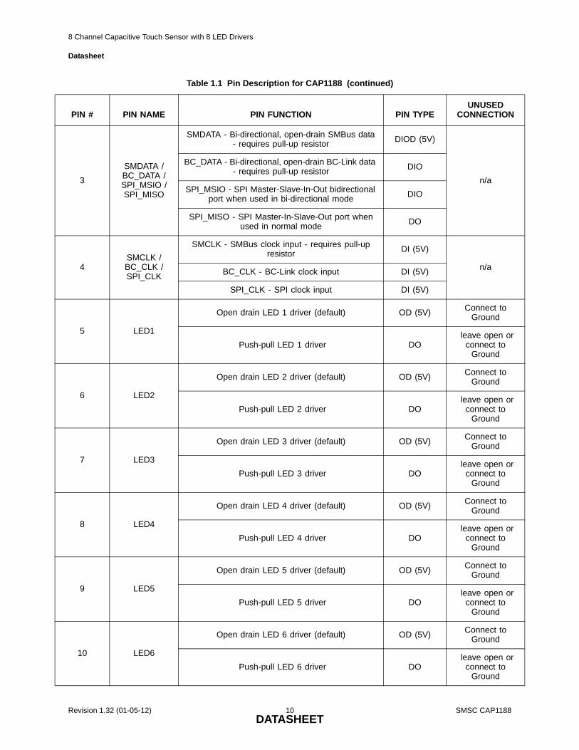

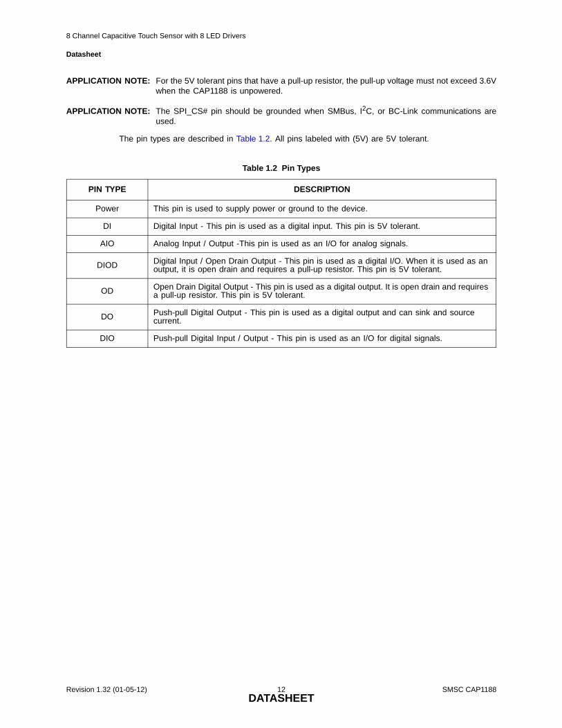


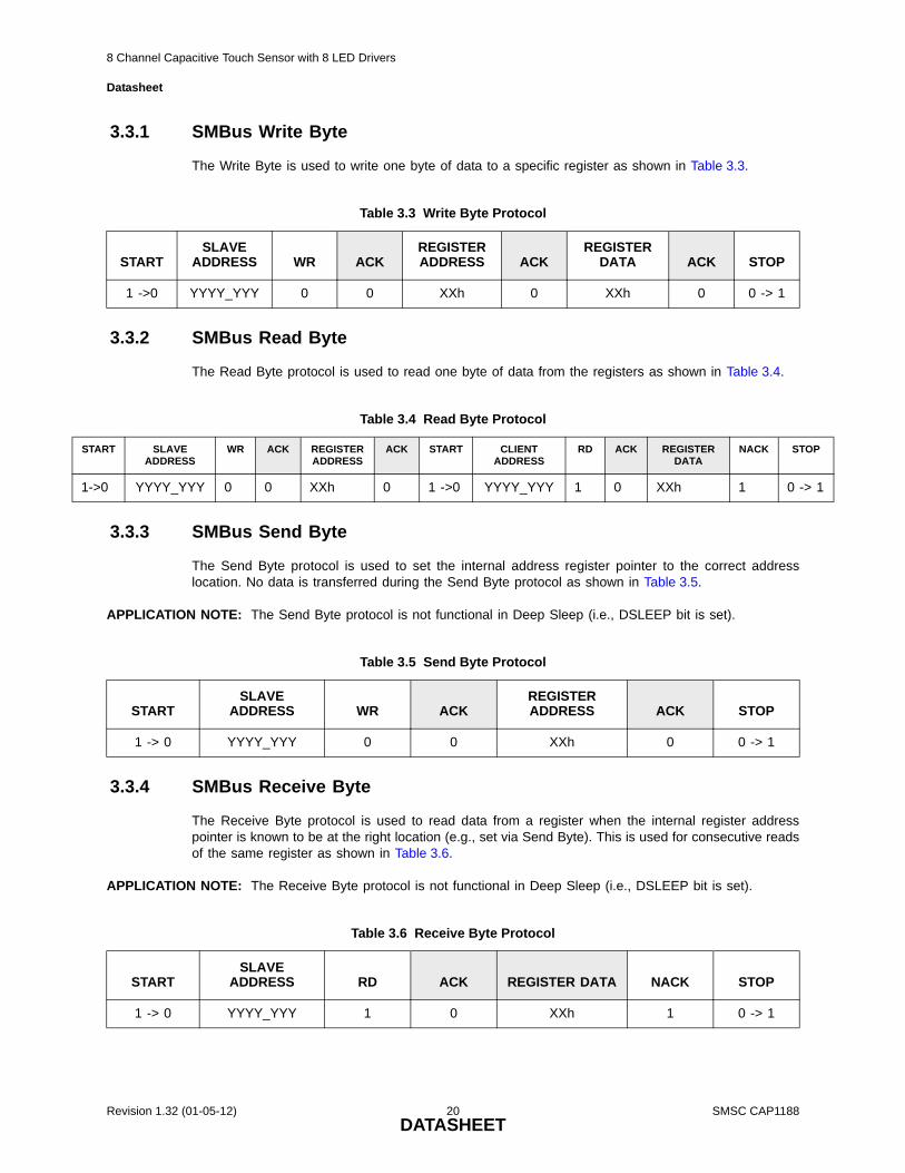

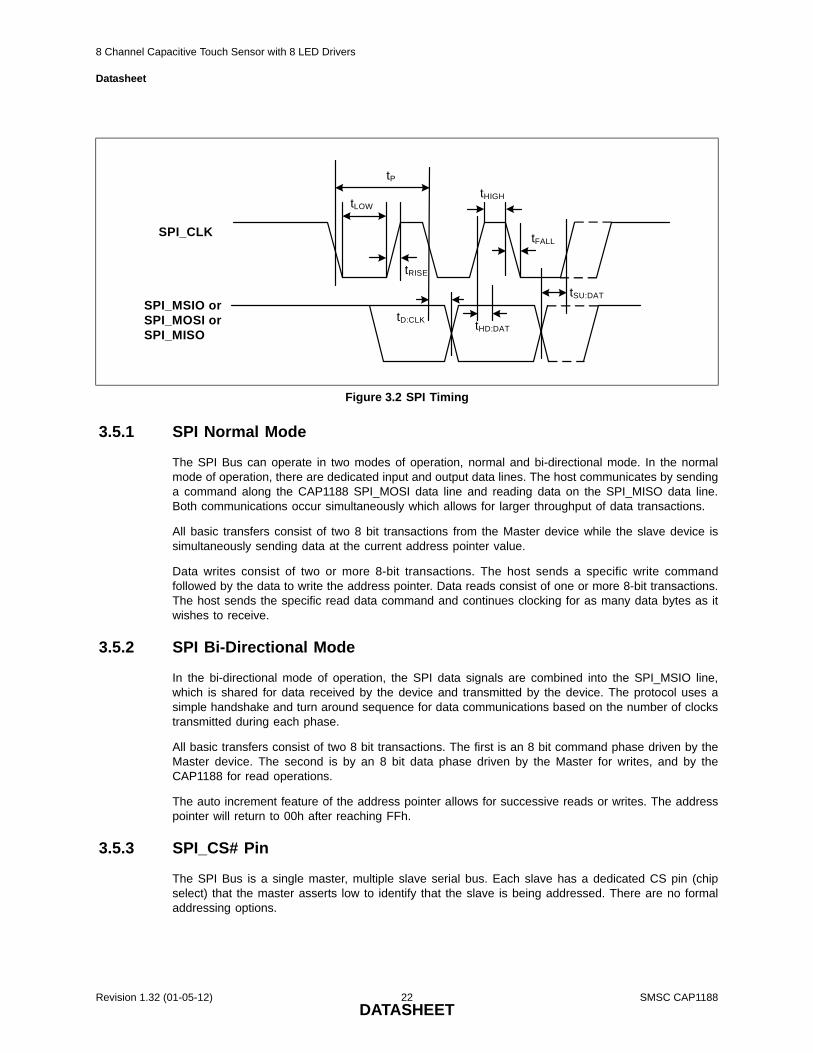


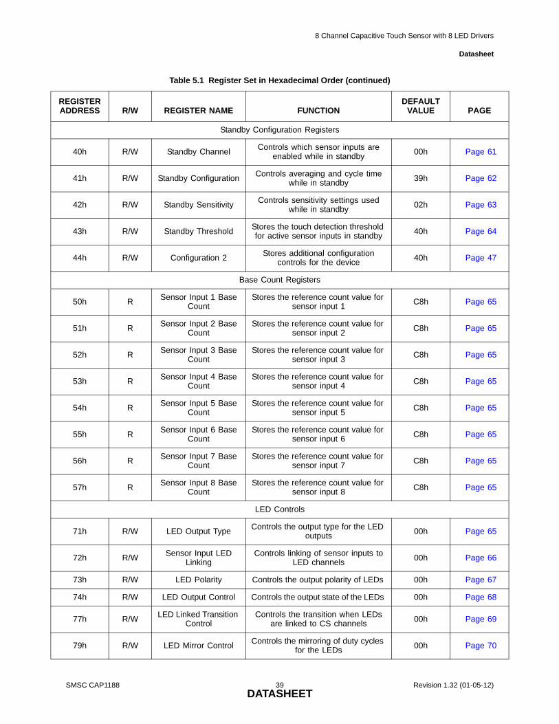


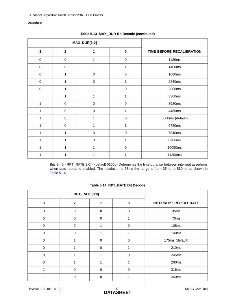


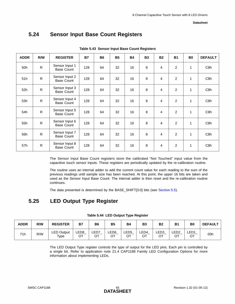


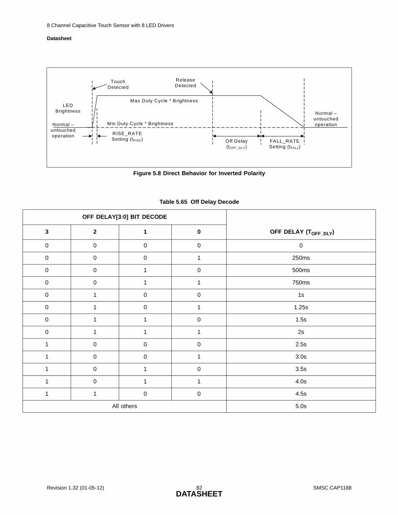


![Atmel AT42AT1010 Datasheet - SparkFun Electronicscdn.sparkfun.com/datasheets/Sensors/Capacitive/AT42QT1010... · AT42QT1010 [DATASHEET] 6 9541I–AT42–05/2013 The value of Cs also](https://static.documents.pub/doc/80x56/5adbb9da7f8b9afc0f8e3c8c/atmel-at42at1010-datasheet-sparkfun-datasheet-6-9541iat42052013-the-value.jpg)


