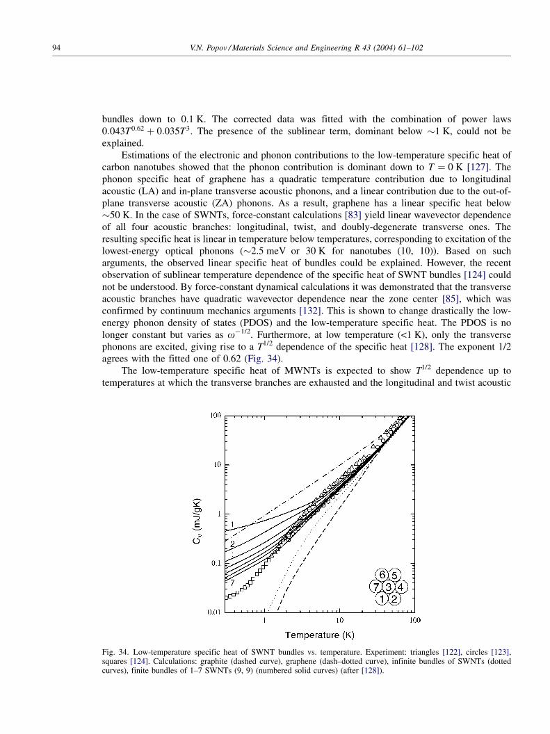
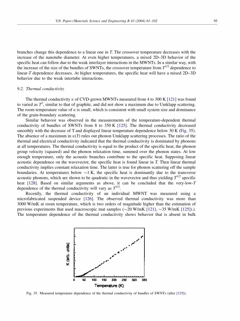
Carbon nanotubes: properties and application Valentin N. Popov 1 Laboratoire de Physique du Solide, Faculte ´s Universitaires Notre-Dame de la Paix, B-5000 Namur, Belgium Abstract Carbon nanotubes are unique tubular structures of nanometer diameter and large length/diameter ratio. The nanotubes may consist of one up to tens and hundreds of concentric shells of carbons with adjacent shells separation of 0.34 nm. The carbon network of the shells is closely related to the honeycomb arrangement of the carbon atoms in the graphite sheets. The amazing mechanical and electronic properties of the nanotubes stem in their quasi-one- dimensional (1D) structure and the graphite-like arrangement of the carbon atoms in the shells. Thus, the nanotubes have high Young’s modulus and tensile strength, which makes them preferable for composite materials with improved mechanical properties. The nanotubes can be metallic or semiconducting depending on their structural parameters. This opens the ways for application of the nanotubes as central elements in electronic devices including field-effect transistors (FET), single-electron transistors and rectifying diodes. Possibilities for using of the nanotubes as high-capacity hydrogen storage media were also considered. This report is intended to summarize some of the major achievements in the field of the carbon nanotube research both experimental and theoretical in connection with the possible industrial applications of the nanotubes. # 2003 Published by Elsevier B.V. Keywords: Carbon nanotubes; Synthesis; Growth; Optical properties; Transport; Vibrational properties; Thermal properties; Nanodevices 1. Introduction Elemental carbon in the sp 2 hybridization can form a variety of amazing structures. Apart from the well-known graphite, carbon can build closed and open cages with honeycomb atomic arrangement. First such structure to be discovered was the C 60 molecule by Kroto et al. [1]. Although various carbon cages were studied, it was only in 1991, when Iijima [2] observed for the first time tubular carbon structures. The nanotubes consisted of up to several tens of graphitic shells (so-called multi-walled carbon nanotubes (MWNTs)) with adjacent shell separation of 0.34 nm, diameters of 1 nm and large length/diameter ratio. Two years later, Iijima and Ichihashi [3] and Bethune et al. [4] synthesized single-walled carbon nanotubes (SWNTs) (Fig. 1). Nowadays, MWNTs and SWNTs are produced mainly by three techniques: arc-discharge, laser-ablation, and catalytic growth. The synthesized nanotube samples are characterized by means of Raman, electronic, and optical spectroscopies. Important information is derived by mechanical, electrical and thermal measure- ments. The experimental data is discussed in comparison with the results of theoretical models and computer simulations (see, e.g. [7–9]). Materials Science and Engineering R 43 (2004) 61–102 E-mail address: [email protected] (V.N. Popov). 1 Permanent address: Faculty of Physics, University of Sofia, BG-1164 Sofia, Bulgaria. 0927-796X/$ – see front matter # 2003 Published by Elsevier B.V. doi:10.1016/j.mser.2003.10.001
Transcript
Carbon nanotubes: properties and application
Valentin N. Popov1
Laboratoire de Physique du Solide, Facultes Universitaires Notre-Dame de la Paix, B-5000 Namur, Belgium
Abstract
Carbon nanotubes are unique tubular structures of nanometer diameter and large length/diameter ratio. The
nanotubes may consist of one up to tens and hundreds of concentric shells of carbons with adjacent shells separation
of �0.34 nm. The carbon network of the shells is closely related to the honeycomb arrangement of the carbon atoms
in the graphite sheets. The amazing mechanical and electronic properties of the nanotubes stem in their quasi-one-
dimensional (1D) structure and the graphite-like arrangement of the carbon atoms in the shells. Thus, the nanotubes
have high Young’s modulus and tensile strength, which makes them preferable for composite materials with
improved mechanical properties. The nanotubes can be metallic or semiconducting depending on their structural
parameters. This opens the ways for application of the nanotubes as central elements in electronic devices including
field-effect transistors (FET), single-electron transistors and rectifying diodes. Possibilities for using of the
nanotubes as high-capacity hydrogen storage media were also considered. This report is intended to summarize
some of the major achievements in the field of the carbon nanotube research both experimental and theoretical in
connection with the possible industrial applications of the nanotubes.
Elemental carbon in the sp2 hybridization can form a variety of amazing structures. Apart fromthe well-known graphite, carbon can build closed and open cages with honeycomb atomicarrangement. First such structure to be discovered was the C60 molecule by Kroto et al. [1]. Althoughvarious carbon cages were studied, it was only in 1991, when Iijima [2] observed for the first timetubular carbon structures. The nanotubes consisted of up to several tens of graphitic shells (so-calledmulti-walled carbon nanotubes (MWNTs)) with adjacent shell separation of �0.34 nm, diameters of�1 nm and large length/diameter ratio. Two years later, Iijima and Ichihashi [3] and Bethune et al.[4] synthesized single-walled carbon nanotubes (SWNTs) (Fig. 1). Nowadays, MWNTs and SWNTsare produced mainly by three techniques: arc-discharge, laser-ablation, and catalytic growth. Thesynthesized nanotube samples are characterized by means of Raman, electronic, and opticalspectroscopies. Important information is derived by mechanical, electrical and thermal measure-ments. The experimental data is discussed in comparison with the results of theoretical models andcomputer simulations (see, e.g. [7–9]).
Materials Science and Engineering R 43 (2004) 61–102
E-mail address: [email protected] (V.N. Popov).1 Permanent address: Faculty of Physics, University of Sofia, BG-1164 Sofia, Bulgaria.
0927-796X/$ – see front matter # 2003 Published by Elsevier B.V.
doi:10.1016/j.mser.2003.10.001
Along with the improvement of the production and characterization techniques for nanotubes,progress is being made in their application. The estimated high Young’s modulus and tensile strengthof the nanotubes has lead to speculations for their possible use in composite materials with improvedmechanical properties [10]. Nanotubes are suitable as electron field emitters because of theirnanosize, structural perfection, high electrical conductivity, and chemical stability with anapplication in flat panel displays [11]. Multiwall nanotubes have been used to electro-catalize anoxygen reduction reaction, which is important for fuel cells [12]. Electrochemically Li-intercalatedSWNT materials showed large irreversible capacities and voltage hysteresis which is an advantagefor using them as battery electrodes [13]. The extraordinary high and reversible hydrogen adsorptionin SWNT materials has attracted much attention because of the possibility of using nanotubes ashigh-capacity hydrogen storage media [14]. It was proposed to use nanotubes as central elements ofelectronic devices including field-effect transistors, single-electron transistors and rectifying diodes[15] and for logic circuits [16].
This paper is intended to summarize the major achievements in the field of the nanotuberesearch both experimental and theoretical in connection with the possible industrial applications ofthe nanotubes. The paper is organized as follows. Section 2 focuses on the synthesis of carbon
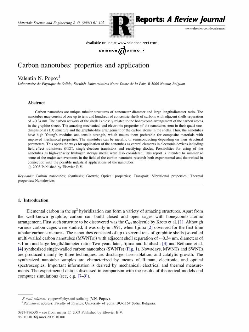
Fig. 1. Schematic representation of the construction of a nanotube by rolling-up an infinite strip of graphite sheet (so-called graphene). In (A) the chiral vector Ch ¼ na1 þ ma2 connects two lattice points O and A on the graphene sheet. Aninfinite strip is cut from the sheet through these two points, perpendicular to the chiral vector. The strip is then rolled-upinto a seamless cylinder. T ¼ t1a1 þ t2a2 is the primitive translation vector of the tube [5]. The nanotube is uniquelyspecified by the pair of integer numbers n, m or by its radius R ¼ Ch=2p and chiral angle y which is the angle between Ch
and the nearest zigzag of C–C bonds. All different tubes have angles y between zero and 308. Special tube types are theachiral tubes (tubes with mirror symmetry): armchair tubes (n, n) (y ¼ 30�) (B(a)) and zigzag tubes (n, 0) (y ¼ 0�) (B(b)).All other tubes are called chiral (B(c)). Details about relations between structural parameters of SWNTs can be foundin [6].
62 V.N. Popov / Materials Science and Engineering R 43 (2004) 61–102
nanotubes. Section 3 considers possible growth mechanisms of nanotubes. Section 4 deals with theelectronic band structure of the nanotubes and their optical properties. Section 5 reviews transportthrough ideal nanotubes and Section 6 considers transport through nanotube junctions. Section 7presents the theory of the phonon dispersion in nanotubes and Raman spectroscopy. Section 8surveys the mechanical properties of nanotubes. Finally, Section 9 deals with the thermal propertiesof nanotubes. The report ends with a summary.
2. Synthesis of CNTs
The MWNTs were first discovered in the soot of the arc-discharge method by Iijima [2]. Thismethod has been used long before that in the production of carbon fibers and fullerenes. It took 2years to Iijima and Ichihashi [3], and Bethune et al. [4] to synthesize SWNTs by use of metalcatalysts in the arc-discharge method in 1993. A significant progress was achieved by laser-ablationsynthesis of bundles of aligned SWNTs with small diameter distribution by Smalley and co-workers[17]. Catalytic growth of nanotubes by the chemical vapor decomposition (CVD) method was firstused by Yacaman et al. [18]. The industrial application of the carbon nanotubes requires thedevelopment of techniques for large-scale production of defect-free nanotubes. In this section, themajor progress in the in the nanotube production methods will be outlined, first, in historical plan,and, secondly, the three main production techniques will be considered separately.
2.1. Arc-discharge
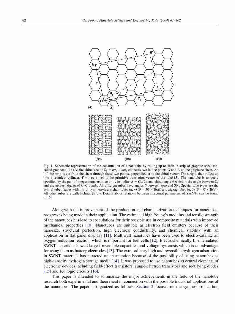
In 1991, Iijima reported the preparation of a new type of finite carbon structures consisting ofneedle-like tubes [2]. The tubes were produced using an arc-discharge evaporation method similar tothat used for the fullerene synthesis. The carbon needles, ranging from 4 to 30 nm in diameter and upto 1 mm in length, were grown on the negative end of the carbon electrode used for the direct current(dc) arc-discharge evaporation of carbon in an argon-filled vessel (100 Torr) (see Fig. 2).Transmission electron microscopy (TEM) revealed that each of the needles comprised coaxial tubesof graphitic sheets, ranging in number from 2 to about 50, later called multi-walled carbonnanotubes. On each of the tubes the carbon-atom hexagons were arranged in a helical fashion about
Fig. 2. Arc-discharge scheme. Two graphite electrodes are used to produce a dc electric arc-discharge in inert gasatmosphere.
V.N. Popov / Materials Science and Engineering R 43 (2004) 61–102 63
the needle axis. The helical pitch varied from needle to needle and from tube to tube within asingle needle. The tips of the needles were usually closed by curved, polygonal, or cone-shapedcaps. A growth model was proposed in which the individual tubes have spiral growth steps at thetube ends.
The TEM study of the growth morphology of the carbon microtubules synthesized by arc-discharge [19] revealed that there were many variations in shape, especially near the tube tips. Atopological model was constructed in which pentagons and heptagons played a key role in the tube-tip shapes. Iijima et al. [20] proposed a model for an open-ended growth, in which the carbon atomsare captured by the dangling bonds, and a layer-by-layer growth, in which the nanotubes thickens.The nucleation of positive (pentagons) and negative (heptagons) disclinations on open-tube endsresults in changes of growth directions, producing different morphologies.
Large-scale synthesis of MWNTs by a variant of the standard arc-discharge technique wasreported by Ebbesen and Ajayan [21]. A potential of �18 V dc was applied between two thingraphite rods in helium atmosphere. At helium pressure of �500 Torr, the yield of nanotubes wasmaximal of �75% relative to the starting graphitic material. The TEM analysis revealed that thesamples consisted of nanotubes of two or more concentric carbon shells. The nanotubes haddiameters between 2 and 20 nm, and lengths of several micrometers. The tube tips were usuallycapped with pentagons.
In 1993, Iijima and Ichihashi [3] and Bethune et al. [4] almost simultaneously reported the arc-discharge and catalyst-assisted synthesis of SWNTs. Iijima used arc-discharge chamber filled with agas mixture of 10 Torr methane and 40 Torr argon. Two vertical thin electrodes were installed in thecenter of the chamber. The lower electrode, the cathode, had a shallow dip to hold a small piece ofiron during the evaporation. The arc-discharge was generated by running a dc current of 200 A at20 V between the electrodes. The use of the three components—argon, iron and methane, wascritical for the synthesis of SWNTs. The TEM analysis of the obtained specimens revealed thepresence of SWNT threads, which were curved and tangled together to form bundles. The nanotubeshad diameters of �1 nm with a broad diameter distribution between 0.7 and 1.65 nm.
In the arc-discharge synthesis of nanotubes, Bethune et al. [4] used as anodes thin electrodeswith bored holes which were filled with a mixture of pure powdered metals (Fe, Ni or Co) andgraphite. The electrodes were vaporized with a current of 95–105 A in 100–500 Torr of He. TheTEM analysis of the obtained specimens showed that only cobalt-catalyzed nanotubes had single-atomic-layer walls with uniform diameters of 1:2 � 0:1 nm.
Large quantities of SWNTs were generated by the arc-technique by Journet et al. [22]. The arcwas generated between two graphite electrodes in a reactor under helium atmosphere (660 mbar).The anode had a hole drilled in its end, filled with a mixture of metallic catalyst (Ni-Co, Co-Y, orNi-Y) and graphite powder. The arc was created by a current of 100 A at a constant voltage drop of30 V. By scanning electron microscopy (SEM), the deposited material was seen to consist of largeamounts (�80%) of entangled carbon ropes. The high-resolution TEM images showed that the ropeshad diameters from 5 to 20 nm. The tube diameters were around 1.4 nm with average separations of�1.7 nm. The X-ray diffraction (XRD) patterns showed periodic arrangement of the tubes in theropes. The similarity of the X-ray diffraction data by Journet et al. [22] and Thess et al. [17] (laser-ablation, see below) was clearly observed: yields in the range 70–90%, tube diameter around 1.4 nm,crystalline bundles of few tens of nanotubes. This lead to the conclusion of a unique growthmechanism in both cases which does not depend on the details of the experimental conditions, butwhich depends much more on the kinetics of carbon condensation in a non-equilibrium situation.Among the two methods, the arc-discharge one has the advantage of being much cheaper than thelaser-ablation method.
64 V.N. Popov / Materials Science and Engineering R 43 (2004) 61–102
2.2. Laser-ablation
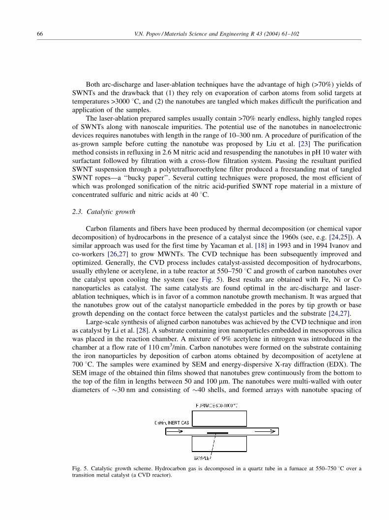
In 1996, Smalley and co-workers produced high yields (>70%) of SWNTs by laser-ablation(vaporization) of graphite rods with small amounts of Ni and Co at 1200 8C [17] (see Fig. 3). The X-ray diffraction and TEM showed that the synthesized nanotubes were remarkably uniform indiameters and that they formed ropes (or bundles) 5–20 nm in diameter and tens to hundreds ofmicrometers long. The ropes formed a two-dimensional (2D) triangular lattice with lattice constanta ¼ 1:7 nm through van der Waals bonding. The ropes were metallic and it was argued that aparticular tube (10, 10), might be the dominant component. The growth of the nanotubes wasexplained by a ‘‘scooter’’ mechanism (Fig. 4). In this mechanism a single Ni or Co atom chemisorbsonto the open edge of a nanotube. The metal atom must have a sufficiently high electronegativity asto prevent formation of fullerenes and it must be highly effective in catalyzing the nanotube growth.The metal atom circulates (‘‘scoots’’) around the open-end of the tube and absorbs small carbonmolecules and converts them into graphite-like sheet. The tube grows until too many catalystatoms aggregate on the end of the nanotube. The large particles either detach or become over-coatedwith sufficient carbon to poison the catalysis. This allows the tube to terminate with a fullerene-liketip or with a catalyst particle. It was argued that the scooter mechanism favors the growth ofarmchair type nanotubes with of most probable type (10, 10) which corresponds to the experimentalobservations.
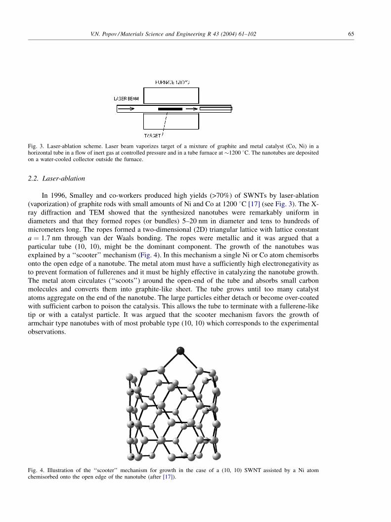
Fig. 3. Laser-ablation scheme. Laser beam vaporizes target of a mixture of graphite and metal catalyst (Co, Ni) in ahorizontal tube in a flow of inert gas at controlled pressure and in a tube furnace at �1200 8C. The nanotubes are depositedon a water-cooled collector outside the furnace.
Fig. 4. Illustration of the ‘‘scooter’’ mechanism for growth in the case of a (10, 10) SWNT assisted by a Ni atomchemisorbed onto the open edge of the nanotube (after [17]).
V.N. Popov / Materials Science and Engineering R 43 (2004) 61–102 65
Both arc-discharge and laser-ablation techniques have the advantage of high (>70%) yields ofSWNTs and the drawback that (1) they rely on evaporation of carbon atoms from solid targets attemperatures >3000 8C, and (2) the nanotubes are tangled which makes difficult the purification andapplication of the samples.
The laser-ablation prepared samples usually contain >70% nearly endless, highly tangled ropesof SWNTs along with nanoscale impurities. The potential use of the nanotubes in nanoelectronicdevices requires nanotubes with length in the range of 10–300 nm. A procedure of purification of theas-grown sample before cutting the nanotube was proposed by Liu et al. [23] The purificationmethod consists in refluxing in 2.6 M nitric acid and resuspending the nanotubes in pH 10 water withsurfactant followed by filtration with a cross-flow filtration system. Passing the resultant purifiedSWNT suspension through a polytetrafluoroethylene filter produced a freestanding mat of tangledSWNT ropes—a ‘‘bucky paper’’. Several cutting techniques were proposed, the most efficient ofwhich was prolonged sonification of the nitric acid-purified SWNT rope material in a mixture ofconcentrated sulfuric and nitric acids at 40 8C.
2.3. Catalytic growth
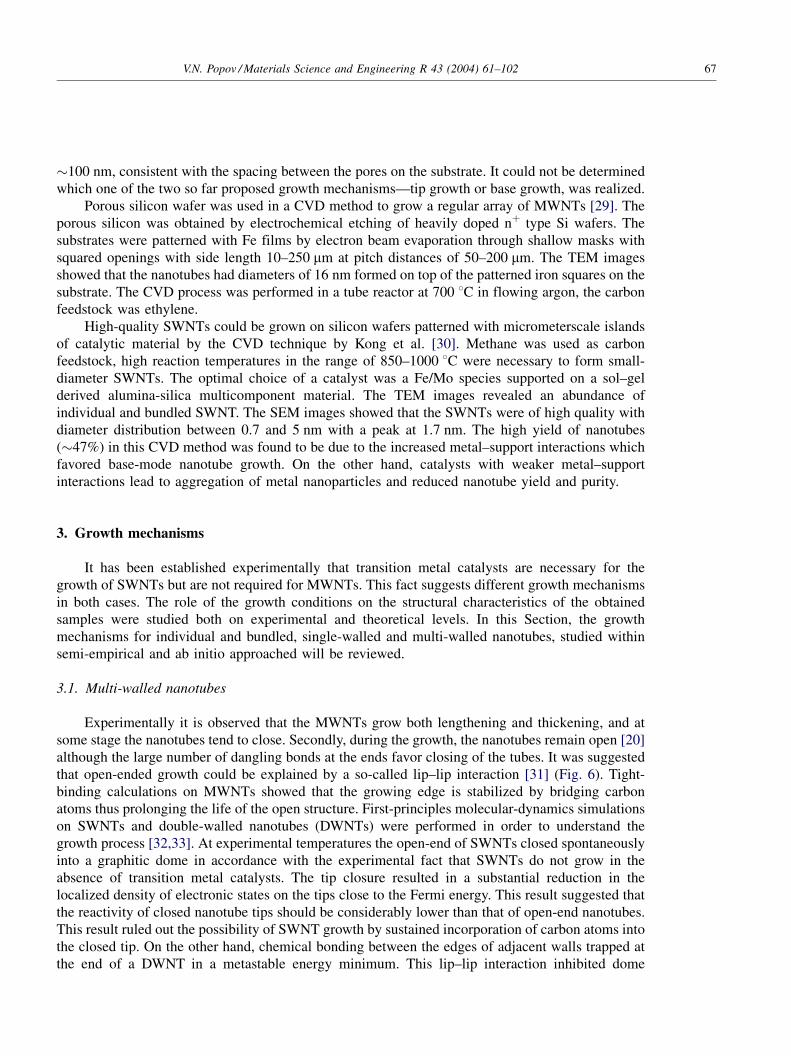
Carbon filaments and fibers have been produced by thermal decomposition (or chemical vapordecomposition) of hydrocarbons in the presence of a catalyst since the 1960s (see, e.g. [24,25]). Asimilar approach was used for the first time by Yacaman et al. [18] in 1993 and in 1994 Ivanov andco-workers [26,27] to grow MWNTs. The CVD technique has been subsequently improved andoptimized. Generally, the CVD process includes catalyst-assisted decomposition of hydrocarbons,usually ethylene or acetylene, in a tube reactor at 550–750 8C and growth of carbon nanotubes overthe catalyst upon cooling the system (see Fig. 5). Best results are obtained with Fe, Ni or Conanoparticles as catalyst. The same catalysts are found optimal in the arc-discharge and laser-ablation techniques, which is in favor of a common nanotube growth mechanism. It was argued thatthe nanotubes grow out of the catalyst nanoparticle embedded in the pores by tip growth or basegrowth depending on the contact force between the catalyst particles and the substrate [24,27].
Large-scale synthesis of aligned carbon nanotubes was achieved by the CVD technique and ironas catalyst by Li et al. [28]. A substrate containing iron nanoparticles embedded in mesoporous silicawas placed in the reaction chamber. A mixture of 9% acetylene in nitrogen was introduced in thechamber at a flow rate of 110 cm3/min. Carbon nanotubes were formed on the substrate containingthe iron nanoparticles by deposition of carbon atoms obtained by decomposition of acetylene at700 8C. The samples were examined by SEM and energy-dispersive X-ray diffraction (EDX). TheSEM image of the obtained thin films showed that nanotubes grew continuously from the bottom tothe top of the film in lengths between 50 and 100 mm. The nanotubes were multi-walled with outerdiameters of �30 nm and consisting of �40 shells, and formed arrays with nanotube spacing of
Fig. 5. Catalytic growth scheme. Hydrocarbon gas is decomposed in a quartz tube in a furnace at 550–750 8C over atransition metal catalyst (a CVD reactor).
66 V.N. Popov / Materials Science and Engineering R 43 (2004) 61–102
�100 nm, consistent with the spacing between the pores on the substrate. It could not be determinedwhich one of the two so far proposed growth mechanisms—tip growth or base growth, was realized.
Porous silicon wafer was used in a CVD method to grow a regular array of MWNTs [29]. Theporous silicon was obtained by electrochemical etching of heavily doped nþ type Si wafers. Thesubstrates were patterned with Fe films by electron beam evaporation through shallow masks withsquared openings with side length 10–250 mm at pitch distances of 50–200 mm. The TEM imagesshowed that the nanotubes had diameters of 16 nm formed on top of the patterned iron squares on thesubstrate. The CVD process was performed in a tube reactor at 700 8C in flowing argon, the carbonfeedstock was ethylene.
High-quality SWNTs could be grown on silicon wafers patterned with micrometerscale islandsof catalytic material by the CVD technique by Kong et al. [30]. Methane was used as carbonfeedstock, high reaction temperatures in the range of 850–1000 8C were necessary to form small-diameter SWNTs. The optimal choice of a catalyst was a Fe/Mo species supported on a sol–gelderived alumina-silica multicomponent material. The TEM images revealed an abundance ofindividual and bundled SWNT. The SEM images showed that the SWNTs were of high quality withdiameter distribution between 0.7 and 5 nm with a peak at 1.7 nm. The high yield of nanotubes(�47%) in this CVD method was found to be due to the increased metal–support interactions whichfavored base-mode nanotube growth. On the other hand, catalysts with weaker metal–supportinteractions lead to aggregation of metal nanoparticles and reduced nanotube yield and purity.
3. Growth mechanisms
It has been established experimentally that transition metal catalysts are necessary for thegrowth of SWNTs but are not required for MWNTs. This fact suggests different growth mechanismsin both cases. The role of the growth conditions on the structural characteristics of the obtainedsamples were studied both on experimental and theoretical levels. In this Section, the growthmechanisms for individual and bundled, single-walled and multi-walled nanotubes, studied withinsemi-empirical and ab initio approached will be reviewed.
3.1. Multi-walled nanotubes
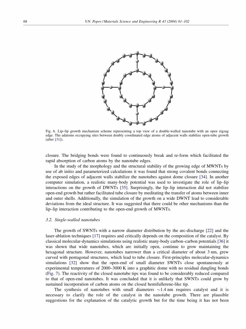
Experimentally it is observed that the MWNTs grow both lengthening and thickening, and atsome stage the nanotubes tend to close. Secondly, during the growth, the nanotubes remain open [20]although the large number of dangling bonds at the ends favor closing of the tubes. It was suggestedthat open-ended growth could be explained by a so-called lip–lip interaction [31] (Fig. 6). Tight-binding calculations on MWNTs showed that the growing edge is stabilized by bridging carbonatoms thus prolonging the life of the open structure. First-principles molecular-dynamics simulationson SWNTs and double-walled nanotubes (DWNTs) were performed in order to understand thegrowth process [32,33]. At experimental temperatures the open-end of SWNTs closed spontaneouslyinto a graphitic dome in accordance with the experimental fact that SWNTs do not grow in theabsence of transition metal catalysts. The tip closure resulted in a substantial reduction in thelocalized density of electronic states on the tips close to the Fermi energy. This result suggested thatthe reactivity of closed nanotube tips should be considerably lower than that of open-end nanotubes.This result ruled out the possibility of SWNT growth by sustained incorporation of carbon atoms intothe closed tip. On the other hand, chemical bonding between the edges of adjacent walls trapped atthe end of a DWNT in a metastable energy minimum. This lip–lip interaction inhibited dome
V.N. Popov / Materials Science and Engineering R 43 (2004) 61–102 67
closure. The bridging bonds were found to continuously break and re-form which facilitated therapid absorption of carbon atoms by the nanotube edges.
In the study of the morphology and the structural stability of the growing edge of MWNTs byuse of ab initio and parameterized calculations it was found that strong covalent bonds connectingthe exposed edges of adjacent walls stabilize the nanotubes against dome closure [34]. In anothercomputer simulation, a realistic many-body potential was used to investigate the role of lip–lipinteractions on the growth of DWNTs [35]. Surprisingly, the lip–lip interaction did not stabilizeopen-end growth but rather facilitated tube closure by meditating the transfer of atoms between innerand outer shells. Additionally, the simulation of the growth on a wide DWNT lead to considerabledeviations from the ideal structure. It was suggested that there could be other mechanisms than thelip–lip interaction contributing to the open-end growth of MWNTs.
3.2. Single-walled nanotubes
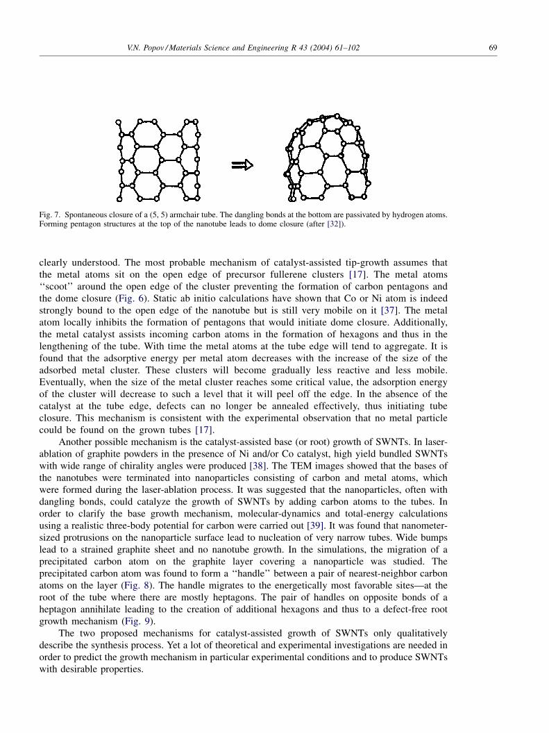
The growth of SWNTs with a narrow diameter distribution by the arc-discharge [22] and thelaser-ablation techniques [17] requires and critically depends on the composition of the catalyst. Byclassical molecular-dynamics simulations using realistic many-body carbon–carbon potentials [36] itwas shown that wide nanotubes, which are initially open, continue to grow maintaining thehexagonal structure. However, nanotubes narrower than a critical diameter of about 3 nm, grewcurved with pentagonal structures, which lead to tube closure. First-principles molecular-dynamicssimulations [32] show that the open-end of small diameter SWNTs close spontaneously atexperimental temperatures of 2000–3000 K into a graphitic dome with no residual dangling bonds(Fig. 7). The reactivity of the closed nanotube tips was found to be considerably reduced comparedto that of open-end nanotubes. It was concluded that it is unlikely that SWNTs could grow bysustained incorporation of carbon atoms on the closed hemifullerene-like tip.
The synthesis of nanotubes with small diameters �1.4 nm requires catalyst and it isnecessary to clarify the role of the catalyst in the nanotube growth. There are plausiblesuggestions for the explanation of the catalytic growth but for the time being it has not been
Fig. 6. Lip–lip growth mechanism scheme representing a top view of a double-walled nanotube with an open zigzagedge. The adatoms occupying sites between doubly coordinated edge atoms of adjacent walls stabilize open-tube growth(after [31]).
68 V.N. Popov / Materials Science and Engineering R 43 (2004) 61–102
clearly understood. The most probable mechanism of catalyst-assisted tip-growth assumes thatthe metal atoms sit on the open edge of precursor fullerene clusters [17]. The metal atoms‘‘scoot’’ around the open edge of the cluster preventing the formation of carbon pentagons andthe dome closure (Fig. 6). Static ab initio calculations have shown that Co or Ni atom is indeedstrongly bound to the open edge of the nanotube but is still very mobile on it [37]. The metalatom locally inhibits the formation of pentagons that would initiate dome closure. Additionally,the metal catalyst assists incoming carbon atoms in the formation of hexagons and thus in thelengthening of the tube. With time the metal atoms at the tube edge will tend to aggregate. It isfound that the adsorptive energy per metal atom decreases with the increase of the size of theadsorbed metal cluster. These clusters will become gradually less reactive and less mobile.Eventually, when the size of the metal cluster reaches some critical value, the adsorption energyof the cluster will decrease to such a level that it will peel off the edge. In the absence of thecatalyst at the tube edge, defects can no longer be annealed effectively, thus initiating tubeclosure. This mechanism is consistent with the experimental observation that no metal particlecould be found on the grown tubes [17].
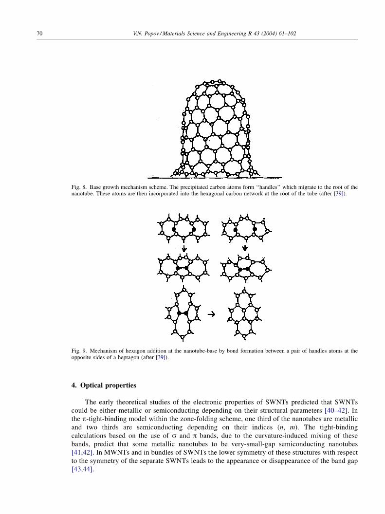
Another possible mechanism is the catalyst-assisted base (or root) growth of SWNTs. In laser-ablation of graphite powders in the presence of Ni and/or Co catalyst, high yield bundled SWNTswith wide range of chirality angles were produced [38]. The TEM images showed that the bases ofthe nanotubes were terminated into nanoparticles consisting of carbon and metal atoms, whichwere formed during the laser-ablation process. It was suggested that the nanoparticles, often withdangling bonds, could catalyze the growth of SWNTs by adding carbon atoms to the tubes. Inorder to clarify the base growth mechanism, molecular-dynamics and total-energy calculationsusing a realistic three-body potential for carbon were carried out [39]. It was found that nanometer-sized protrusions on the nanoparticle surface lead to nucleation of very narrow tubes. Wide bumpslead to a strained graphite sheet and no nanotube growth. In the simulations, the migration of aprecipitated carbon atom on the graphite layer covering a nanoparticle was studied. Theprecipitated carbon atom was found to form a ‘‘handle’’ between a pair of nearest-neighbor carbonatoms on the layer (Fig. 8). The handle migrates to the energetically most favorable sites—at theroot of the tube where there are mostly heptagons. The pair of handles on opposite bonds of aheptagon annihilate leading to the creation of additional hexagons and thus to a defect-free rootgrowth mechanism (Fig. 9).
The two proposed mechanisms for catalyst-assisted growth of SWNTs only qualitativelydescribe the synthesis process. Yet a lot of theoretical and experimental investigations are needed inorder to predict the growth mechanism in particular experimental conditions and to produce SWNTswith desirable properties.
Fig. 7. Spontaneous closure of a (5, 5) armchair tube. The dangling bonds at the bottom are passivated by hydrogen atoms.Forming pentagon structures at the top of the nanotube leads to dome closure (after [32]).
V.N. Popov / Materials Science and Engineering R 43 (2004) 61–102 69
4. Optical properties
The early theoretical studies of the electronic properties of SWNTs predicted that SWNTscould be either metallic or semiconducting depending on their structural parameters [40–42]. Inthe p-tight-binding model within the zone-folding scheme, one third of the nanotubes are metallicand two thirds are semiconducting depending on their indices (n, m). The tight-bindingcalculations based on the use of s and p bands, due to the curvature-induced mixing of thesebands, predict that some metallic nanotubes to be very-small-gap semiconducting nanotubes[41,42]. In MWNTs and in bundles of SWNTs the lower symmetry of these structures with respectto the symmetry of the separate SWNTs leads to the appearance or disappearance of the band gap[43,44].
Fig. 8. Base growth mechanism scheme. The precipitated carbon atoms form ‘‘handles’’ which migrate to the root of thenanotube. These atoms are then incorporated into the hexagonal carbon network at the root of the tube (after [39]).
Fig. 9. Mechanism of hexagon addition at the nanotube-base by bond formation between a pair of handles atoms at theopposite sides of a heptagon (after [39]).
70 V.N. Popov / Materials Science and Engineering R 43 (2004) 61–102
4.1. Electronic band structure of SWNTs
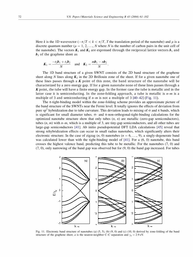
The band structure of the ‘‘rolled-up’’ SWNTs can be studied in a good approximationwithin the tight-binding model in the zone-folding scheme [42]. The band structure of a singlegraphene sheet is considered as a starting point. The unit cell of the sheet contains two carbonatoms, each carbon atom having four valence electrons. Therefore, a tight-binding model yieldseight bands: four valence bands and four conduction bands. One s orbital and two in-plane porbitals of each carbon atom are sp2-hybridized. Due to the different symmetry of the sp2-hybridized orbitals and pz orbitals, the matrix elements of the Hamiltonian and the overlap matrixelements between such orbitals vanish. The sp2-hybridized orbitals form the so-called s valencebands and s* conduction bands. The pz orbitals of the carbon atoms, oriented perpendicularly tothe sheet (z-direction), form the p valence band and the p* conduction band. Therefore, theproblem for the band structure of a graphite sheet conveniently splits into a problem for the s ands* bands, and a problem for the p and p* bands. The latter problem is of major importance for theresonant Raman scattering and we will focus on it. The resulting band structure of graphene(Fig. 10) is characterized with p and p* bands degenerate at the K points in the hexagonal Brillouinzone of the sheet. This degenerate energy level corresponds to the Fermi energy, which shows thatthe graphene sheet is a zero-gap metal. On rolling-up a graphene strip into a cylindrical nanotube, theband structure of the nanotube can be derived from that of the graphene sheet by the zone-foldingmethod.
The one-dimensional (1D) band structure of a (n, m) nanotube is given by the zone-foldingrelation by use of the two-dimensional band structure of graphene [8]
Ekm ¼ E2D kK2
jK2jþ mK1
� �:
Fig. 10. The electronic band structure of a graphite sheet calculated within a p-band tight-binding model. The valence pand conduction p* bands show degeneracy at the K points in the Brillouin zone at the Fermi level.
V.N. Popov / Materials Science and Engineering R 43 (2004) 61–102 71
with diameters larger than 1 nm, the rehybridization effects were unimportant. The structuraloptimization of the nanotubes had little effect on the band structure. Tubes with diameters larger than0.4 nm were found to be stable.
4.2. Electronic density of states of SWNTs
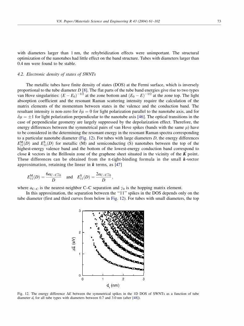
The metallic tubes have finite density of states (DOS) at the Fermi surface, which is inverselyproportional to the tube diameter D [8]. The flat parts of the tube band energies give rise to two typesvan Hove singularities: ðE � E0Þ�1/2 at the zone bottom and ðE0 � EÞ�1/2 at the zone top. The lightabsorption coefficient and the resonant Raman scattering intensity require the calculation of thematrix elements of the momentum between states in the valence and the conduction band. Theresultant intensity is non-zero for dm ¼ 0 for light polarization parallel to the nanotube axis, and fordm ¼ �1 for light polarization perpendicular to the nanotube axis [46]. The optical transitions in thecase of perpendicular geometry are largely suppressed by the depolarization effect. Therefore, theenergy differences between the symmetrical pairs of van Hove spikes (bands with the same m) haveto be considered in the determining the resonant energy in the resonant Raman spectra correspondingto a particular nanotube diameter (Fig. 12). For tubes with large diameters D, the energy differencesEM
11ðDÞ and ES11ðDÞ for metallic (M) and semiconducting (S) nanotubes between the top of the
highest-energy valence band and the bottom of the lowest-energy conduction band correspond toclose k vectors in the Brillouin zone of the graphene sheet situated in the vicinity of the K point.These differences can be obtained from the p-tight-binding formula in the small k-vectorapproximation, retaining the linear in k terms, as [47]
EM11ðDÞ ¼ 6aC�Cg0
Dand ES
11ðDÞ ¼ 2aC�Cg0
D;
where aC–C is the nearest-neighbor C–C separation and g0 is the hopping matrix element.In this approximation, the separation between the ‘‘11’’ spikes in the DOS depends only on the
tube diameter (first and third curves from below in Fig. 12). For tubes with small diameters, the top
Fig. 12. The energy difference DE between the symmetrical spikes in the 1D DOS of SWNTs as a function of tubediameter dt for all tube types with diameters between 0.7 and 3.0 nm (after [48]).
V.N. Popov / Materials Science and Engineering R 43 (2004) 61–102 73
and the bottom of the mentioned conduction and valence bands, respectively, correspond to points inthe Brillouin zone of the graphene sheet, for which the band energy is no longer isotropic. The equi-energy lines become triangles, a distortion known in structures with three-fold symmetry axis as thetrigonal warping effect. The energy differences EM
11ðDÞ and ES11ðDÞ will then depend on the direction
of the tube axis on the graphite sheet and will therefore depend on the tube chirality as well. In thecase of metallic nanotubes, the warping effect gives rise to DOS splitting of the first valence andconduction band spikes which is largest for zigzag nanotubes and zero for armchair nanotubes whilehaving intermediate values for chiral nanotubes. The DOS splitting yields widening of thedifferences EM
11ðDÞ and ES11ðDÞ for small diameter tubes. The trigonal warping effect is important for
metallic zigzag nanotubes with D < 2 nm. Semiconducting nanotubes do not show trigonal warpingeffect.
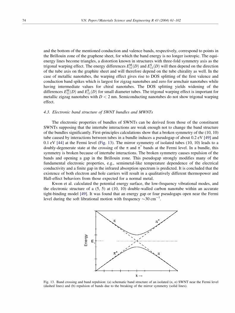
4.3. Electronic band structure of SWNT bundles and MWNTs
The electronic properties of bundles of SWNTs can be derived from those of the constituentSWNTs supposing that the intertube interactions are weak enough not to change the band structureof the bundles significantly. First-principles calculations show that a broken symmetry of the (10, 10)tube caused by interactions between tubes in a bundle induces a pseudogap of about 0.2 eV [49] and0.1 eV [44] at the Fermi level (Fig. 13). The mirror symmetry of isolated tubes (10, 10) leads to adoubly-degenerate state at the crossing of the p and p* bands at the Fermi level. In a bundle, thissymmetry is broken because of intertube interactions. The broken symmetry causes repulsion of thebands and opening a gap in the Brillouin zone. This pseudogap strongly modifies many of thefundamental electronic properties, e.g., semimetal-like temperature dependence of the electricalconductivity and a finite gap in the infrared absorption spectrum is predicted. It is concluded that theexistence of both electron and hole carriers will result in a qualitatively different thermopower andHall-effect behaviors from those expected for a normal metal.
Kwon et al. calculated the potential energy surface, the low-frequency vibrational modes, andthe electronic structure of a (5, 5) at (10, 10) double-walled carbon nanotube within an accuratetight-binding model [49]. It was found that an energy gap or four pseudogaps open near the Fermilevel during the soft librational motion with frequency �30 cm�1.
Fig. 13. Band crossing and band repulsion: (a) schematic band structure of an isolated (n, n) SWNT near the Fermi level(dashed lines) and (b) repulsion of bands due to the breaking of the mirror symmetry (solid lines).
74 V.N. Popov / Materials Science and Engineering R 43 (2004) 61–102
Recently, an extensive ab initio local-density-functional study of the electronic dispersion inchiral and achiral isolated and bundled SWNTs was reported [50]. The curvature of the nanotubeswas found to reduce the band gap by hybridization and to alter the electronic states responsible forthe optical transitions. Even for wide nanotubes (D ¼ 1:0–1.5 nm) the energy-levels shift was�0.1 eV. Bundling of the nanotubes resulted in a further decrease of the energy gap insemiconducting tubes. The (10, 0) bundle was found to be metallic. It is concluded that theobtained intertube dispersion of �0.1 eV could broaden the electronic density of states and theoptical absorption bands in bundles.
4.4. Optical absorption
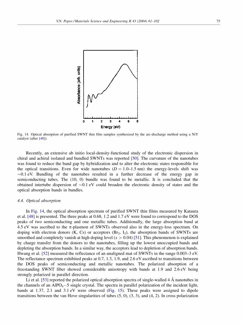
In Fig. 14, the optical absorption spectrum of purified SWNT thin films measured by Katauraet al. [48] is presented. The three peaks at 0.68, 1.2 and 1.7 eV were found to correspond to the DOSpeaks of two semiconducting and one metallic tubes. Additionally, the large absorption band at4.5 eV was ascribed to the p-plasmon of SWNTs observed also in the energy-loss spectrum. Ondoping with electron donors (K, Cs) or acceptors (Br2, I2), the absorption bands of SWNTs aresmoothed and completely vanish at high doping level (x > 0:04) [51]. This phenomenon is explainedby charge transfer from the donors to the nanotubes, filling up the lowest unoccupied bands anddepleting the absorption bands. In a similar way, the acceptors lead to depletion of absorption bands.Hwang et al. [52] measured the reflectance of an unaligned mat of SWNTs in the range 0.003–3 eV.The reflectance spectrum exhibited peaks at 0.7, 1.3, 1.9, and 2.6 eV ascribed to transitions betweenthe DOS peaks of semiconducting and metallic nanotubes. The polarized absorption of afreestanding SWNT fiber showed considerable anisotropy with bands at 1.9 and 2.6 eV beingstrongly polarized in parallel direction.
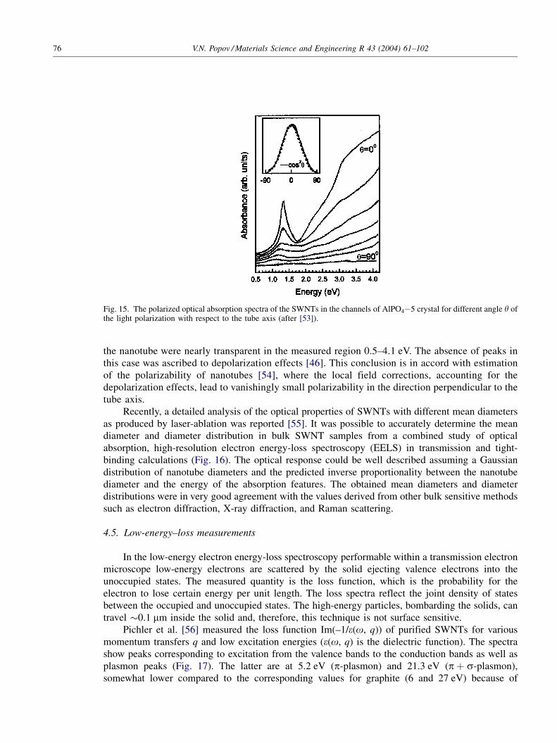
Li et al. [53] reported the polarized optical absorption spectra of single-walled 4 A nanotubes inthe channels of an AlPO4�5 single crystal. The spectra in parallel polarization of the incident light,bands at 1.37, 2.1 and 3.1 eV were observed (Fig. 15). These peaks were assigned to dipoletransitions between the van Hove singularities of tubes (5, 0), (3, 3), and (4, 2). In cross polarization
Fig. 14. Optical absorption of purified SWNT thin film samples synthesized by the arc-discharge method using a NiYcatalyst (after [48]).
V.N. Popov / Materials Science and Engineering R 43 (2004) 61–102 75
the nanotube were nearly transparent in the measured region 0.5–4.1 eV. The absence of peaks inthis case was ascribed to depolarization effects [46]. This conclusion is in accord with estimationof the polarizability of nanotubes [54], where the local field corrections, accounting for thedepolarization effects, lead to vanishingly small polarizability in the direction perpendicular to thetube axis.
Recently, a detailed analysis of the optical properties of SWNTs with different mean diametersas produced by laser-ablation was reported [55]. It was possible to accurately determine the meandiameter and diameter distribution in bulk SWNT samples from a combined study of opticalabsorption, high-resolution electron energy-loss spectroscopy (EELS) in transmission and tight-binding calculations (Fig. 16). The optical response could be well described assuming a Gaussiandistribution of nanotube diameters and the predicted inverse proportionality between the nanotubediameter and the energy of the absorption features. The obtained mean diameters and diameterdistributions were in very good agreement with the values derived from other bulk sensitive methodssuch as electron diffraction, X-ray diffraction, and Raman scattering.
4.5. Low-energy–loss measurements
In the low-energy electron energy-loss spectroscopy performable within a transmission electronmicroscope low-energy electrons are scattered by the solid ejecting valence electrons into theunoccupied states. The measured quantity is the loss function, which is the probability for theelectron to lose certain energy per unit length. The loss spectra reflect the joint density of statesbetween the occupied and unoccupied states. The high-energy particles, bombarding the solids, cantravel �0.1 mm inside the solid and, therefore, this technique is not surface sensitive.
Pichler et al. [56] measured the loss function Im(–1/e(o, q)) of purified SWNTs for variousmomentum transfers q and low excitation energies (e(o, q) is the dielectric function). The spectrashow peaks corresponding to excitation from the valence bands to the conduction bands as well asplasmon peaks (Fig. 17). The latter are at 5.2 eV (p-plasmon) and 21.3 eV (pþ s-plasmon),somewhat lower compared to the corresponding values for graphite (6 and 27 eV) because of
Fig. 15. The polarized optical absorption spectra of the SWNTs in the channels of AlPO4�5 crystal for different angle y ofthe light polarization with respect to the tube axis (after [53]).
76 V.N. Popov / Materials Science and Engineering R 43 (2004) 61–102
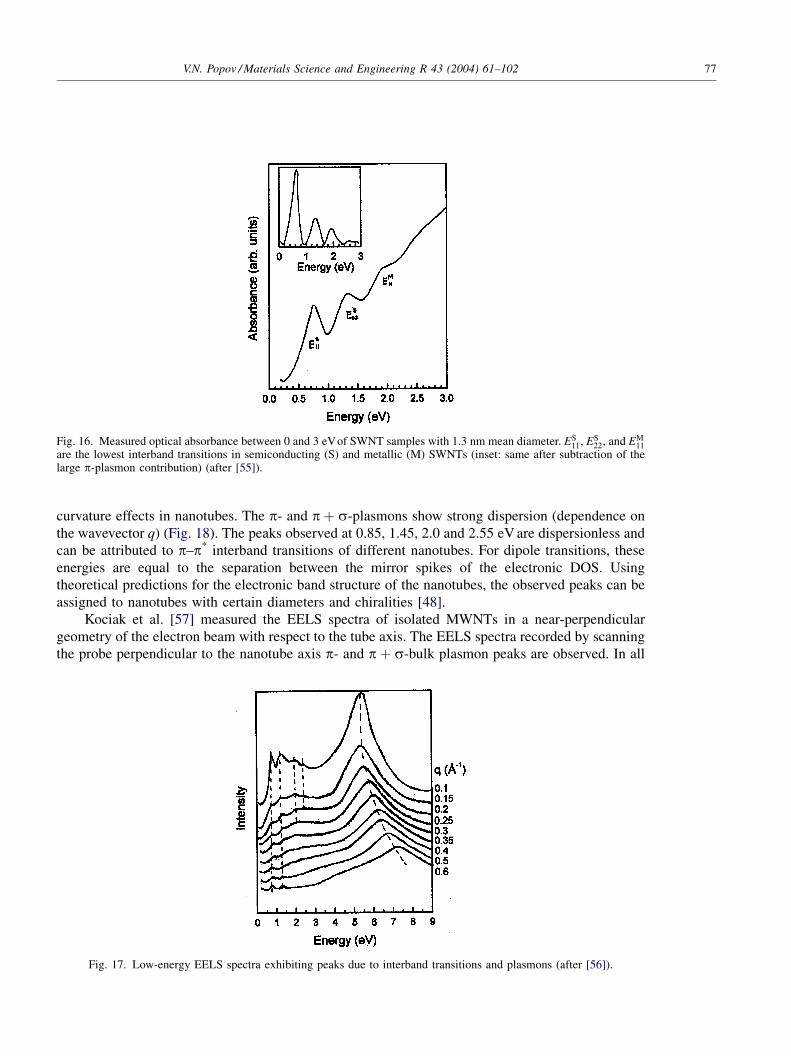
curvature effects in nanotubes. The p- and pþ s-plasmons show strong dispersion (dependence onthe wavevector q) (Fig. 18). The peaks observed at 0.85, 1.45, 2.0 and 2.55 eV are dispersionless andcan be attributed to p–p* interband transitions of different nanotubes. For dipole transitions, theseenergies are equal to the separation between the mirror spikes of the electronic DOS. Usingtheoretical predictions for the electronic band structure of the nanotubes, the observed peaks can beassigned to nanotubes with certain diameters and chiralities [48].
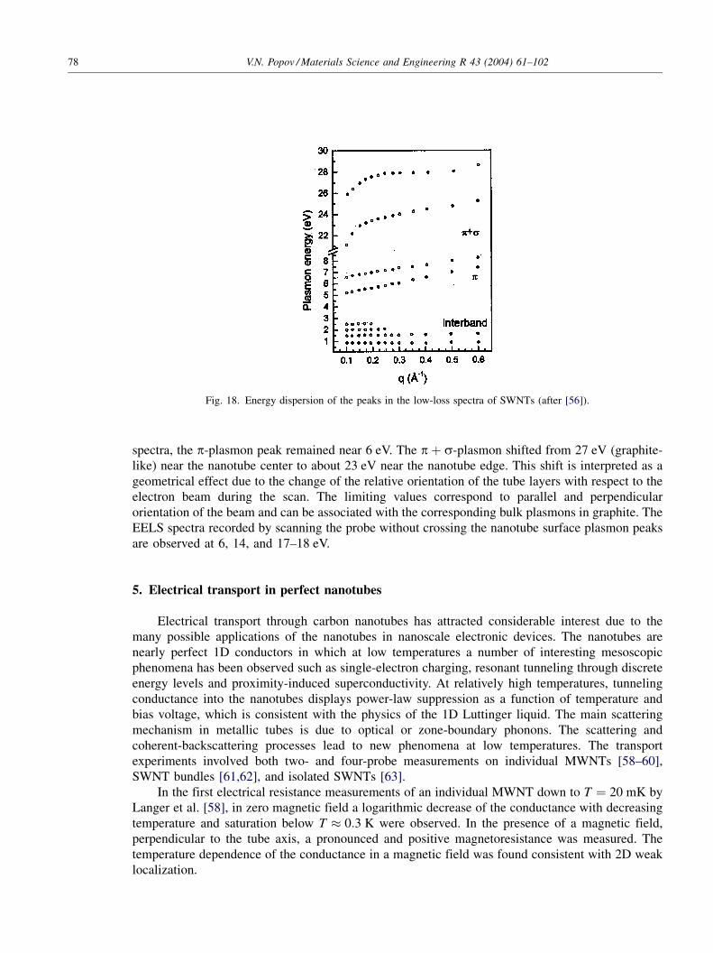
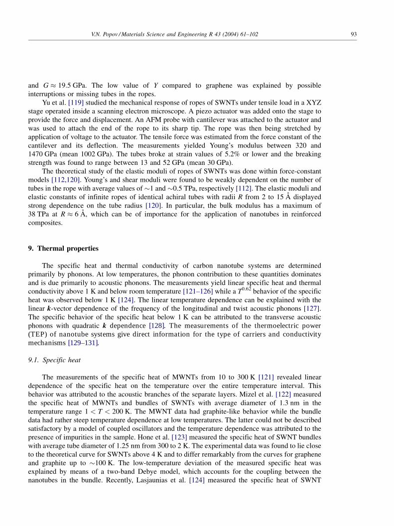
Kociak et al. [57] measured the EELS spectra of isolated MWNTs in a near-perpendiculargeometry of the electron beam with respect to the tube axis. The EELS spectra recorded by scanningthe probe perpendicular to the nanotube axis p- and pþ s-bulk plasmon peaks are observed. In all
Fig. 16. Measured optical absorbance between 0 and 3 eVof SWNT samples with 1.3 nm mean diameter. ES11, ES
22, and EM11
are the lowest interband transitions in semiconducting (S) and metallic (M) SWNTs (inset: same after subtraction of thelarge p-plasmon contribution) (after [55]).
Fig. 17. Low-energy EELS spectra exhibiting peaks due to interband transitions and plasmons (after [56]).
V.N. Popov / Materials Science and Engineering R 43 (2004) 61–102 77
spectra, the p-plasmon peak remained near 6 eV. The pþ s-plasmon shifted from 27 eV (graphite-like) near the nanotube center to about 23 eV near the nanotube edge. This shift is interpreted as ageometrical effect due to the change of the relative orientation of the tube layers with respect to theelectron beam during the scan. The limiting values correspond to parallel and perpendicularorientation of the beam and can be associated with the corresponding bulk plasmons in graphite. TheEELS spectra recorded by scanning the probe without crossing the nanotube surface plasmon peaksare observed at 6, 14, and 17–18 eV.
5. Electrical transport in perfect nanotubes
Electrical transport through carbon nanotubes has attracted considerable interest due to themany possible applications of the nanotubes in nanoscale electronic devices. The nanotubes arenearly perfect 1D conductors in which at low temperatures a number of interesting mesoscopicphenomena has been observed such as single-electron charging, resonant tunneling through discreteenergy levels and proximity-induced superconductivity. At relatively high temperatures, tunnelingconductance into the nanotubes displays power-law suppression as a function of temperature andbias voltage, which is consistent with the physics of the 1D Luttinger liquid. The main scatteringmechanism in metallic tubes is due to optical or zone-boundary phonons. The scattering andcoherent-backscattering processes lead to new phenomena at low temperatures. The transportexperiments involved both two- and four-probe measurements on individual MWNTs [58–60],SWNT bundles [61,62], and isolated SWNTs [63].
In the first electrical resistance measurements of an individual MWNT down to T ¼ 20 mK byLanger et al. [58], in zero magnetic field a logarithmic decrease of the conductance with decreasingtemperature and saturation below T 0:3 K were observed. In the presence of a magnetic field,perpendicular to the tube axis, a pronounced and positive magnetoresistance was measured. Thetemperature dependence of the conductance in a magnetic field was found consistent with 2D weaklocalization.
Fig. 18. Energy dispersion of the peaks in the low-loss spectra of SWNTs (after [56]).
78 V.N. Popov / Materials Science and Engineering R 43 (2004) 61–102
5.1. Electrical transport in bundles of SWNTs
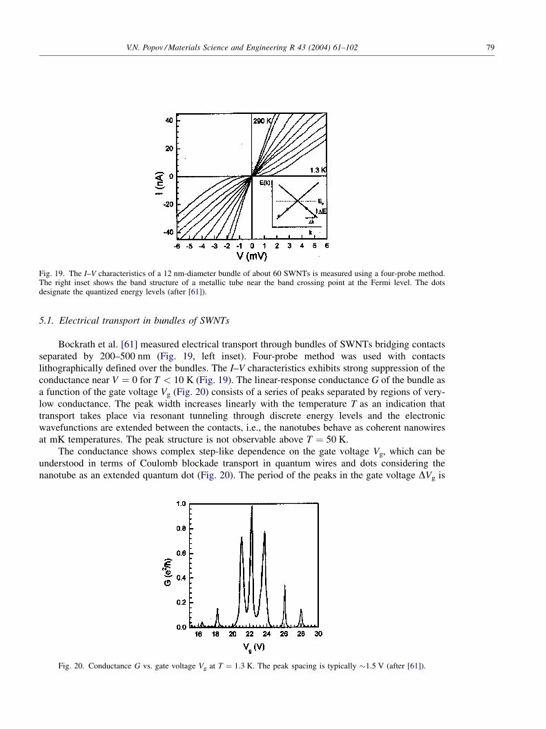
Bockrath et al. [61] measured electrical transport through bundles of SWNTs bridging contactsseparated by 200–500 nm (Fig. 19, left inset). Four-probe method was used with contactslithographically defined over the bundles. The I–V characteristics exhibits strong suppression of theconductance near V ¼ 0 for T < 10 K (Fig. 19). The linear-response conductance G of the bundle asa function of the gate voltage Vg (Fig. 20) consists of a series of peaks separated by regions of very-low conductance. The peak width increases linearly with the temperature T as an indication thattransport takes place via resonant tunneling through discrete energy levels and the electronicwavefunctions are extended between the contacts, i.e., the nanotubes behave as coherent nanowiresat mK temperatures. The peak structure is not observable above T ¼ 50 K.
The conductance shows complex step-like dependence on the gate voltage Vg, which can beunderstood in terms of Coulomb blockade transport in quantum wires and dots considering thenanotube as an extended quantum dot (Fig. 20). The period of the peaks in the gate voltage DVg is
Fig. 19. The I–V characteristics of a 12 nm-diameter bundle of about 60 SWNTs is measured using a four-probe method.The right inset shows the band structure of a metallic tube near the band crossing point at the Fermi level. The dotsdesignate the quantized energy levels (after [61]).
Fig. 20. Conductance G vs. gate voltage Vg at T ¼ 1:3 K. The peak spacing is typically �1.5 V (after [61]).
V.N. Popov / Materials Science and Engineering R 43 (2004) 61–102 79
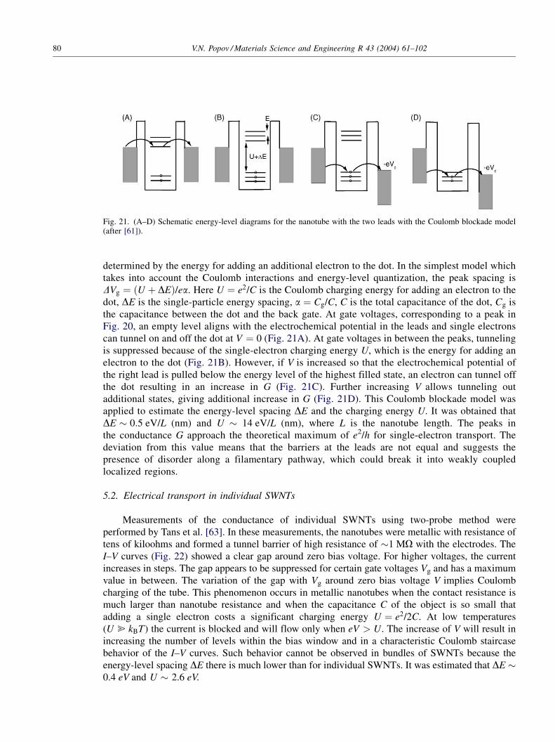
determined by the energy for adding an additional electron to the dot. In the simplest model whichtakes into account the Coulomb interactions and energy-level quantization, the peak spacing isDVg ¼ ðU þ DEÞ/ea. Here U ¼ e2/C is the Coulomb charging energy for adding an electron to thedot, DE is the single-particle energy spacing, a ¼ Cg/C, C is the total capacitance of the dot, Cg isthe capacitance between the dot and the back gate. At gate voltages, corresponding to a peak inFig. 20, an empty level aligns with the electrochemical potential in the leads and single electronscan tunnel on and off the dot at V ¼ 0 (Fig. 21A). At gate voltages in between the peaks, tunnelingis suppressed because of the single-electron charging energy U, which is the energy for adding anelectron to the dot (Fig. 21B). However, if V is increased so that the electrochemical potential ofthe right lead is pulled below the energy level of the highest filled state, an electron can tunnel offthe dot resulting in an increase in G (Fig. 21C). Further increasing V allows tunneling outadditional states, giving additional increase in G (Fig. 21D). This Coulomb blockade model wasapplied to estimate the energy-level spacing DE and the charging energy U. It was obtained thatDE � 0:5 eV/L (nm) and U � 14 eV/L (nm), where L is the nanotube length. The peaks inthe conductance G approach the theoretical maximum of e2/h for single-electron transport. Thedeviation from this value means that the barriers at the leads are not equal and suggests thepresence of disorder along a filamentary pathway, which could break it into weakly coupledlocalized regions.
5.2. Electrical transport in individual SWNTs
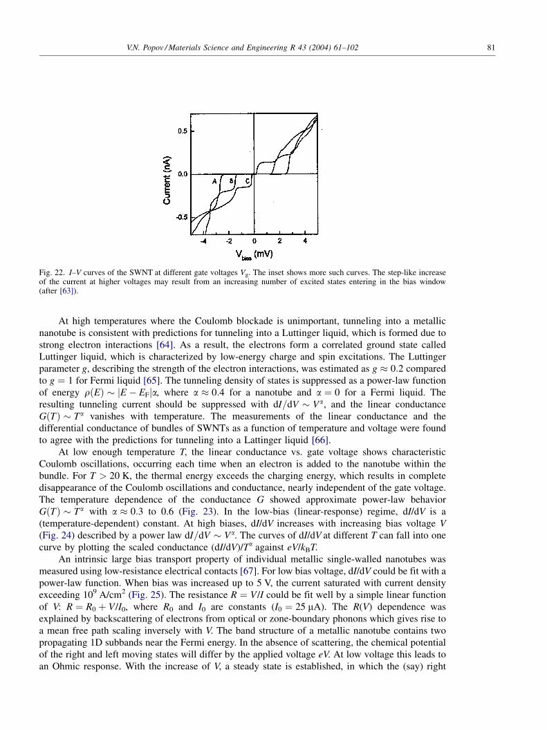
Measurements of the conductance of individual SWNTs using two-probe method wereperformed by Tans et al. [63]. In these measurements, the nanotubes were metallic with resistance oftens of kiloohms and formed a tunnel barrier of high resistance of �1 MO with the electrodes. TheI–V curves (Fig. 22) showed a clear gap around zero bias voltage. For higher voltages, the currentincreases in steps. The gap appears to be suppressed for certain gate voltages Vg and has a maximumvalue in between. The variation of the gap with Vg around zero bias voltage V implies Coulombcharging of the tube. This phenomenon occurs in metallic nanotubes when the contact resistance ismuch larger than nanotube resistance and when the capacitance C of the object is so small thatadding a single electron costs a significant charging energy U ¼ e2/2C. At low temperatures(U @ kBT) the current is blocked and will flow only when eV > U. The increase of V will result inincreasing the number of levels within the bias window and in a characteristic Coulomb staircasebehavior of the I–V curves. Such behavior cannot be observed in bundles of SWNTs because theenergy-level spacing DE there is much lower than for individual SWNTs. It was estimated that DE �0.4 eV and U � 2.6 eV.
Fig. 21. (A–D) Schematic energy-level diagrams for the nanotube with the two leads with the Coulomb blockade model(after [61]).
80 V.N. Popov / Materials Science and Engineering R 43 (2004) 61–102
At high temperatures where the Coulomb blockade is unimportant, tunneling into a metallicnanotube is consistent with predictions for tunneling into a Luttinger liquid, which is formed due tostrong electron interactions [64]. As a result, the electrons form a correlated ground state calledLuttinger liquid, which is characterized by low-energy charge and spin excitations. The Luttingerparameter g, describing the strength of the electron interactions, was estimated as g 0:2 comparedto g ¼ 1 for Fermi liquid [65]. The tunneling density of states is suppressed as a power-law functionof energy rðEÞ � jE � EFja, where a 0:4 for a nanotube and a ¼ 0 for a Fermi liquid. Theresulting tunneling current should be suppressed with dI=dV � Va, and the linear conductanceGðTÞ � Ta vanishes with temperature. The measurements of the linear conductance and thedifferential conductance of bundles of SWNTs as a function of temperature and voltage were foundto agree with the predictions for tunneling into a Lattinger liquid [66].
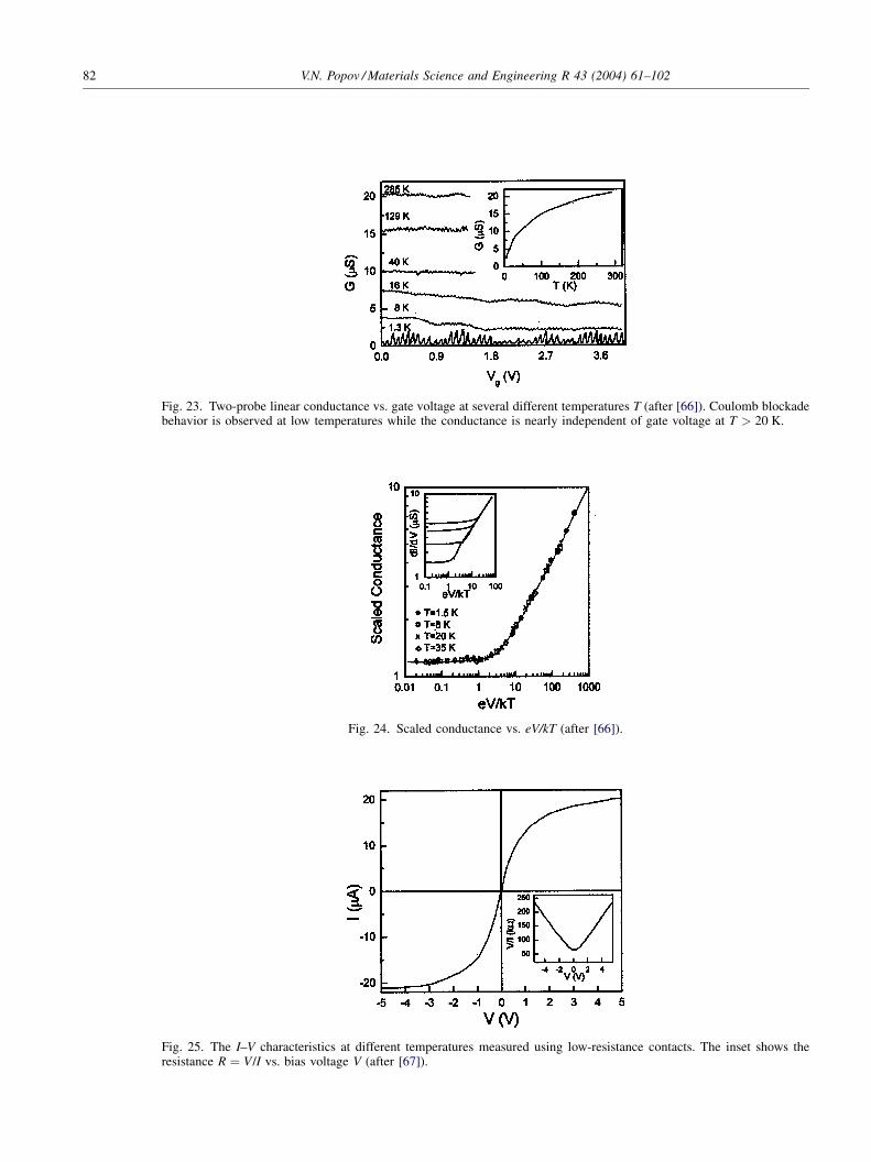
At low enough temperature T, the linear conductance vs. gate voltage shows characteristicCoulomb oscillations, occurring each time when an electron is added to the nanotube within thebundle. For T > 20 K, the thermal energy exceeds the charging energy, which results in completedisappearance of the Coulomb oscillations and conductance, nearly independent of the gate voltage.The temperature dependence of the conductance G showed approximate power-law behaviorGðTÞ � Ta with a 0:3 to 0.6 (Fig. 23). In the low-bias (linear-response) regime, dI/dV is a(temperature-dependent) constant. At high biases, dI/dV increases with increasing bias voltage V(Fig. 24) described by a power law dI=dV � Va. The curves of dI/dV at different T can fall into onecurve by plotting the scaled conductance (dI/dV)/Ta against eV/kBT.
An intrinsic large bias transport property of individual metallic single-walled nanotubes wasmeasured using low-resistance electrical contacts [67]. For low bias voltage, dI/dV could be fit with apower-law function. When bias was increased up to 5 V, the current saturated with current densityexceeding 109 A/cm2 (Fig. 25). The resistance R ¼ V /I could be fit well by a simple linear functionof V: R ¼ R0 þ V/I0, where R0 and I0 are constants (I0 ¼ 25 mA). The R(V) dependence wasexplained by backscattering of electrons from optical or zone-boundary phonons which gives rise toa mean free path scaling inversely with V. The band structure of a metallic nanotube contains twopropagating 1D subbands near the Fermi energy. In the absence of scattering, the chemical potentialof the right and left moving states will differ by the applied voltage eV. At low voltage this leads toan Ohmic response. With the increase of V, a steady state is established, in which the (say) right
Fig. 22. I–V curves of the SWNT at different gate voltages Vg. The inset shows more such curves. The step-like increaseof the current at higher voltages may result from an increasing number of excited states entering in the bias window(after [63]).
V.N. Popov / Materials Science and Engineering R 43 (2004) 61–102 81
Fig. 23. Two-probe linear conductance vs. gate voltage at several different temperatures T (after [66]). Coulomb blockadebehavior is observed at low temperatures while the conductance is nearly independent of gate voltage at T > 20 K.
Fig. 24. Scaled conductance vs. eV/kT (after [66]).
Fig. 25. The I–V characteristics at different temperatures measured using low-resistance contacts. The inset shows theresistance R ¼ V/I vs. bias voltage V (after [67]).
82 V.N. Popov / Materials Science and Engineering R 43 (2004) 61–102
moving electrons are populated to an energy hO higher than the left moving ones. Assuming strongelectron–phonon coupling, the high-energy electrons are backscattered by emitting optical or zone-boundary phonons of energy hO. This mechanism leads to a saturation current I0 ¼ ð4e=hÞhO. For atypical phonon energy of hO ¼ 0:16 eV, the saturation current is found to be I0 ¼ 25 mA, the same asthe experimentally derived value.
5.3. Nanotube field-effect transistors
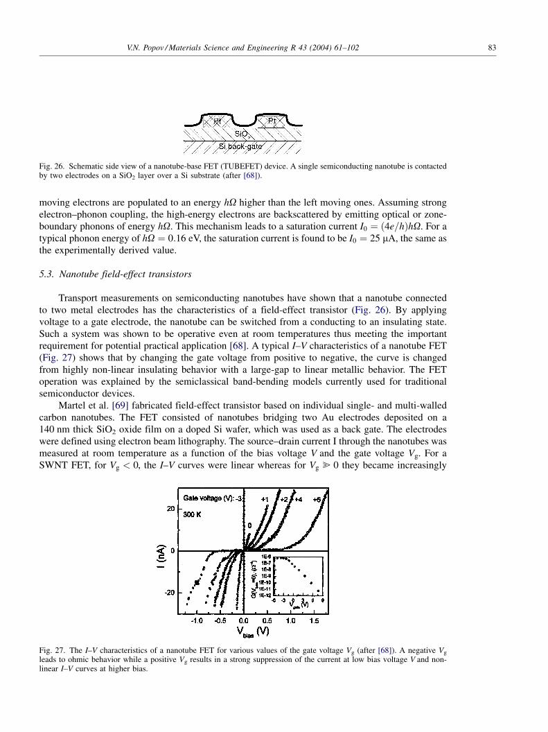
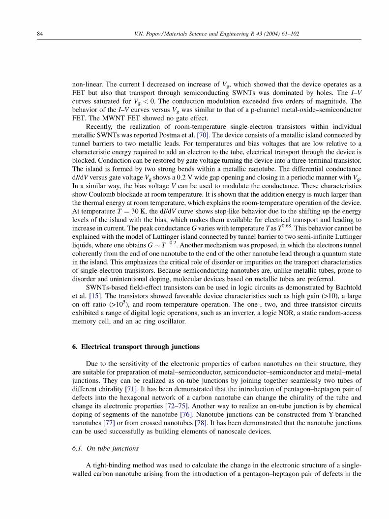
Transport measurements on semiconducting nanotubes have shown that a nanotube connectedto two metal electrodes has the characteristics of a field-effect transistor (Fig. 26). By applyingvoltage to a gate electrode, the nanotube can be switched from a conducting to an insulating state.Such a system was shown to be operative even at room temperatures thus meeting the importantrequirement for potential practical application [68]. A typical I–V characteristics of a nanotube FET(Fig. 27) shows that by changing the gate voltage from positive to negative, the curve is changedfrom highly non-linear insulating behavior with a large-gap to linear metallic behavior. The FEToperation was explained by the semiclassical band-bending models currently used for traditionalsemiconductor devices.
Martel et al. [69] fabricated field-effect transistor based on individual single- and multi-walledcarbon nanotubes. The FET consisted of nanotubes bridging two Au electrodes deposited on a140 nm thick SiO2 oxide film on a doped Si wafer, which was used as a back gate. The electrodeswere defined using electron beam lithography. The source–drain current I through the nanotubes wasmeasured at room temperature as a function of the bias voltage V and the gate voltage Vg. For aSWNT FET, for Vg < 0, the I–V curves were linear whereas for Vg @ 0 they became increasingly
Fig. 26. Schematic side view of a nanotube-base FET (TUBEFET) device. A single semiconducting nanotube is contactedby two electrodes on a SiO2 layer over a Si substrate (after [68]).
Fig. 27. The I–V characteristics of a nanotube FET for various values of the gate voltage Vg (after [68]). A negative Vg
leads to ohmic behavior while a positive Vg results in a strong suppression of the current at low bias voltage V and non-linear I–V curves at higher bias.
V.N. Popov / Materials Science and Engineering R 43 (2004) 61–102 83
non-linear. The current I decreased on increase of Vg, which showed that the device operates as aFET but also that transport through semiconducting SWNTs was dominated by holes. The I–Vcurves saturated for Vg < 0. The conduction modulation exceeded five orders of magnitude. Thebehavior of the I–V curves versus Vg was similar to that of a p-channel metal-oxide–semiconductorFET. The MWNT FET showed no gate effect.
Recently, the realization of room-temperature single-electron transistors within individualmetallic SWNTs was reported Postma et al. [70]. The device consists of a metallic island connected bytunnel barriers to two metallic leads. For temperatures and bias voltages that are low relative to acharacteristic energy required to add an electron to the tube, electrical transport through the device isblocked. Conduction can be restored by gate voltage turning the device into a three-terminal transistor.The island is formed by two strong bends within a metallic nanotube. The differential conductancedI/dV versus gate voltage Vg shows a 0.2 V wide gap opening and closing in a periodic manner with Vg.In a similar way, the bias voltage V can be used to modulate the conductance. These characteristicsshow Coulomb blockade at room temperature. It is shown that the addition energy is much larger thanthe thermal energy at room temperature, which explains the room-temperature operation of the device.At temperature T ¼ 30 K, the dI/dV curve shows step-like behavior due to the shifting up the energylevels of the island with the bias, which makes them available for electrical transport and leading toincrease in current. The peak conductance G varies with temperature T as T0.68. This behavior cannot beexplained with the model of Luttinger island connected by tunnel barrier to two semi-infinite Luttingerliquids, where one obtains G � T�0.2. Another mechanism was proposed, in which the electrons tunnelcoherently from the end of one nanotube to the end of the other nanotube lead through a quantum statein the island. This emphasizes the critical role of disorder or impurities on the transport characteristicsof single-electron transistors. Because semiconducting nanotubes are, unlike metallic tubes, prone todisorder and unintentional doping, molecular devices based on metallic tubes are preferred.
SWNTs-based field-effect transistors can be used in logic circuits as demonstrated by Bachtoldet al. [15]. The transistors showed favorable device characteristics such as high gain (>10), a largeon-off ratio (>105), and room-temperature operation. The one-, two, and three-transistor circuitsexhibited a range of digital logic operations, such as an inverter, a logic NOR, a static random-accessmemory cell, and an ac ring oscillator.
6. Electrical transport through junctions
Due to the sensitivity of the electronic properties of carbon nanotubes on their structure, theyare suitable for preparation of metal–semiconductor, semiconductor–semiconductor and metal–metaljunctions. They can be realized as on-tube junctions by joining together seamlessly two tubes ofdifferent chirality [71]. It has been demonstrated that the introduction of pentagon–heptagon pair ofdefects into the hexagonal network of a carbon nanotube can change the chirality of the tube andchange its electronic properties [72–75]. Another way to realize an on-tube junction is by chemicaldoping of segments of the nanotube [76]. Nanotube junctions can be constructed from Y-branchednanotubes [77] or from crossed nanotubes [78]. It has been demonstrated that the nanotube junctionscan be used successfully as building elements of nanoscale devices.
6.1. On-tube junctions
A tight-binding method was used to calculate the change in the electronic structure of a single-walled carbon nanotube arising from the introduction of a pentagon–heptagon pair of defects in the
84 V.N. Popov / Materials Science and Engineering R 43 (2004) 61–102
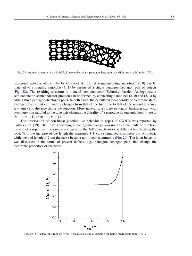
hexagonal network of the tube by Chico et al. [73]. A semiconducting nanotube (8, 0) can bematched to a metallic nanotube (7, 1) by means of a single pentagon–heptagon pair of defects(Fig. 28). The resulting structure is a metal–semiconductor (Schottky) barrier. Analogously, asemiconductor–semiconductor junction can be formed by connecting nanotubes (8, 0) and (5, 3) byadding three pentagon–heptagon pairs. In both cases, the calculated local density of electronic statesaveraged over a unit cell, swiftly changes from that of the first tube to that of the second tube in afew unit cells distance along the junction. More generally, a single pentagon–heptagon pair withsymmetry non-parallel to the tube axis changes the chirality of a nanotube by one unit from (n, m) to(n þ 1, m � 1) or (n � 1, m þ 1).
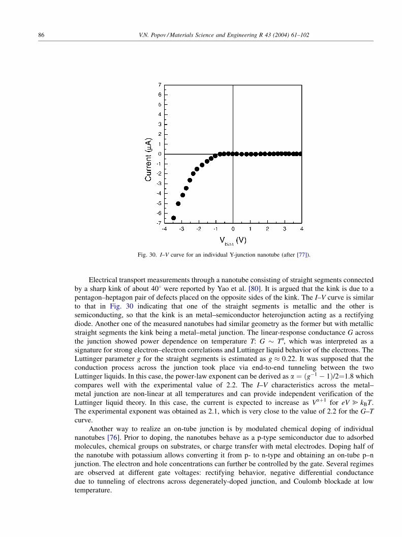
The observation of non-linear junction-like behavior in ropes of SWNTs was reported byCollins et al. [79]. The tip of a scanning tunneling microscope was used as a manipulator to retractthe end of a rope from the sample and measure the I–V characteristics at different length along therope. With the increase of the length the measured I–V curve remained non-linear but symmetricwhile beyond length of 2 mm the curve became non-linear asymmetric (Fig. 29). The latter behaviorwas discussed in the terms of present defects, e.g., pentagon–heptagon pairs that change theelectronic properties of the tubes.
Fig. 28. Atomic structure of a (8, 0)/(7, 1) nanotube with a pentagon–heptagon pair (light gray balls) (after [73]).
Fig. 29. I–V curve of a rope of SWNTs measured using a scanning tunneling microscope (after [79]).
V.N. Popov / Materials Science and Engineering R 43 (2004) 61–102 85
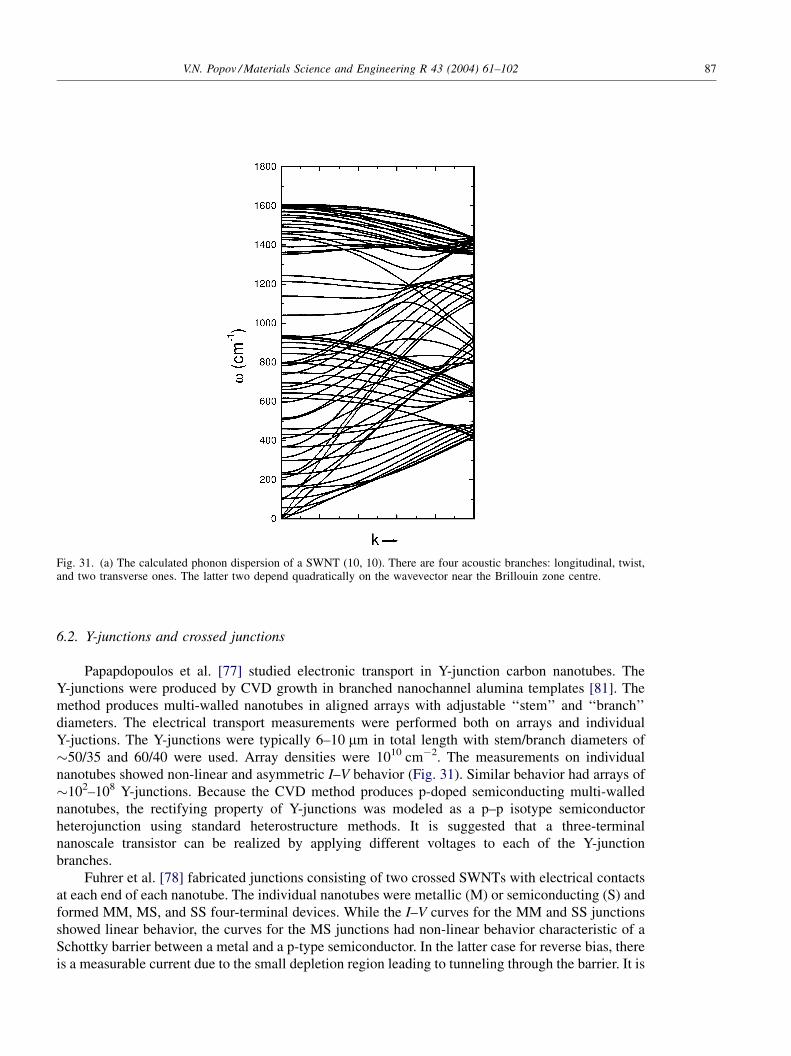
Electrical transport measurements through a nanotube consisting of straight segments connectedby a sharp kink of about 408 were reported by Yao et al. [80]. It is argued that the kink is due to apentagon–heptagon pair of defects placed on the opposite sides of the kink. The I–V curve is similarto that in Fig. 30 indicating that one of the straight segments is metallic and the other issemiconducting, so that the kink is an metal–semiconductor heterojunction acting as a rectifyingdiode. Another one of the measured nanotubes had similar geometry as the former but with metallicstraight segments the kink being a metal–metal junction. The linear-response conductance G acrossthe junction showed power dependence on temperature T: G � Ta, which was interpreted as asignature for strong electron–electron correlations and Luttinger liquid behavior of the electrons. TheLuttinger parameter g for the straight segments is estimated as g 0:22. It was supposed that theconduction process across the junction took place via end-to-end tunneling between the twoLuttinger liquids. In this case, the power-law exponent can be derived as a ¼ ðg�1 � 1Þ/2¼1.8 whichcompares well with the experimental value of 2.2. The I–V characteristics across the metal–metal junction are non-linear at all temperatures and can provide independent verification of theLuttinger liquid theory. In this case, the current is expected to increase as Vaþ1 for eV @ kBT.The experimental exponent was obtained as 2.1, which is very close to the value of 2.2 for the G–T
curve.Another way to realize an on-tube junction is by modulated chemical doping of individual
nanotubes [76]. Prior to doping, the nanotubes behave as a p-type semiconductor due to adsorbedmolecules, chemical groups on substrates, or charge transfer with metal electrodes. Doping half ofthe nanotube with potassium allows converting it from p- to n-type and obtaining an on-tube p–njunction. The electron and hole concentrations can further be controlled by the gate. Several regimesare observed at different gate voltages: rectifying behavior, negative differential conductancedue to tunneling of electrons across degenerately-doped junction, and Coulomb blockade at lowtemperature.
Fig. 30. I–V curve for an individual Y-junction nanotube (after [77]).
86 V.N. Popov / Materials Science and Engineering R 43 (2004) 61–102
6.2. Y-junctions and crossed junctions
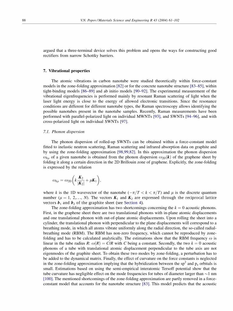
Papapdopoulos et al. [77] studied electronic transport in Y-junction carbon nanotubes. TheY-junctions were produced by CVD growth in branched nanochannel alumina templates [81]. Themethod produces multi-walled nanotubes in aligned arrays with adjustable ‘‘stem’’ and ‘‘branch’’diameters. The electrical transport measurements were performed both on arrays and individualY-juctions. The Y-junctions were typically 6–10 mm in total length with stem/branch diameters of�50/35 and 60/40 were used. Array densities were 1010 cm�2. The measurements on individualnanotubes showed non-linear and asymmetric I–V behavior (Fig. 31). Similar behavior had arrays of�102–108 Y-junctions. Because the CVD method produces p-doped semiconducting multi-wallednanotubes, the rectifying property of Y-junctions was modeled as a p–p isotype semiconductorheterojunction using standard heterostructure methods. It is suggested that a three-terminalnanoscale transistor can be realized by applying different voltages to each of the Y-junctionbranches.
Fuhrer et al. [78] fabricated junctions consisting of two crossed SWNTs with electrical contactsat each end of each nanotube. The individual nanotubes were metallic (M) or semiconducting (S) andformed MM, MS, and SS four-terminal devices. While the I–V curves for the MM and SS junctionsshowed linear behavior, the curves for the MS junctions had non-linear behavior characteristic of aSchottky barrier between a metal and a p-type semiconductor. In the latter case for reverse bias, thereis a measurable current due to the small depletion region leading to tunneling through the barrier. It is
Fig. 31. (a) The calculated phonon dispersion of a SWNT (10, 10). There are four acoustic branches: longitudinal, twist,and two transverse ones. The latter two depend quadratically on the wavevector near the Brillouin zone centre.
V.N. Popov / Materials Science and Engineering R 43 (2004) 61–102 87
branches are linear in k near the Brillouin zone center while the transverse elastic waves in thin rodsare quadratic in k and so should be the transverse acoustic (TA) phonons in nanotubes. The use ofvalence force fields that account for many-body interatomic interactions allows reproducing thisquadratic dependence of the transverse acoustic waves in nanotubes [101] (see Fig. 31). The directcalculations of the phonons in nanotubes are usually based on non-optimized or optimized nanotubestructures. The use of empirical force-constant models does not allow for structural optimization andpredefined structures have to be used [83–85]. The nanotube structure can be optimized within tight-binding models [86–89] and ab initio models [90–92].
Among the various phonons, of greatest importance for the sample characterization are theRBM and the so-called G-band modes because they are observable in the Raman and infraredspectra. The G-band consists of in-plane bond-stretching modes, which originate from the E2g in-plane stretching mode in graphene. In nanotubes, due to symmetry-breaking effects associated withthe nanotube curvature, this E2g mode gives rise to six Raman-active modes (2A1 þ 2E1 þ 2E2) inchiral tubes and to three Raman-active modes (A1g þ E1g þ E2g) in armchair and zigzag tubes. Theforce-constant models usually use insufficient number of force constants, which does not allow forprecise reproduction of the overbending of the highest optical branch of graphene [83–85]. Evenusing force constants, precisely fitted to the phonon dispersion of graphene, the force-constantmodels will not be able to reproduce correctly the splitting between these modes because of thepartial description of the curvature effects. The tight-binding models have the drawback yieldingusually by �10% too high frequencies of the G-band modes [86–89]. Only ab initio models canpredict fairly well the G-band modes [90–92].
7.2. Raman spectroscopy
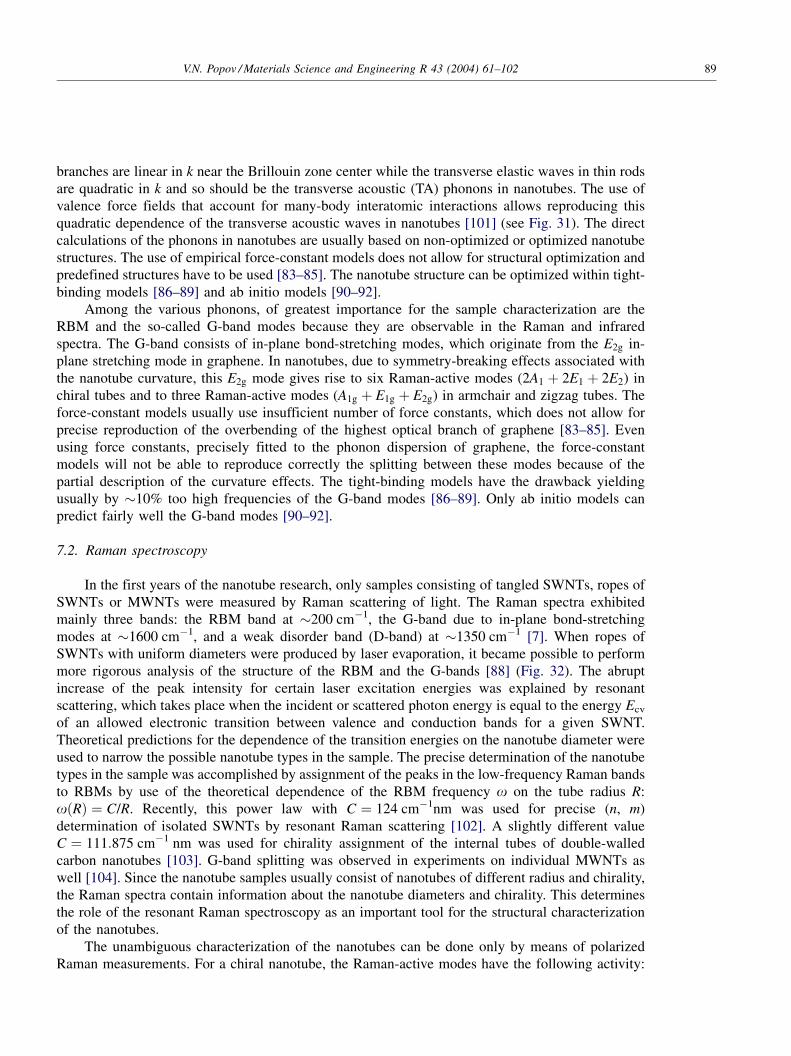
In the first years of the nanotube research, only samples consisting of tangled SWNTs, ropes ofSWNTs or MWNTs were measured by Raman scattering of light. The Raman spectra exhibitedmainly three bands: the RBM band at �200 cm�1, the G-band due to in-plane bond-stretchingmodes at �1600 cm�1, and a weak disorder band (D-band) at �1350 cm�1 [7]. When ropes ofSWNTs with uniform diameters were produced by laser evaporation, it became possible to performmore rigorous analysis of the structure of the RBM and the G-bands [88] (Fig. 32). The abruptincrease of the peak intensity for certain laser excitation energies was explained by resonantscattering, which takes place when the incident or scattered photon energy is equal to the energy Ecv
of an allowed electronic transition between valence and conduction bands for a given SWNT.Theoretical predictions for the dependence of the transition energies on the nanotube diameter wereused to narrow the possible nanotube types in the sample. The precise determination of the nanotubetypes in the sample was accomplished by assignment of the peaks in the low-frequency Raman bandsto RBMs by use of the theoretical dependence of the RBM frequency o on the tube radius R:oðRÞ ¼ C/R. Recently, this power law with C ¼ 124 cm�1nm was used for precise (n, m)determination of isolated SWNTs by resonant Raman scattering [102]. A slightly different valueC ¼ 111:875 cm�1 nm was used for chirality assignment of the internal tubes of double-walledcarbon nanotubes [103]. G-band splitting was observed in experiments on individual MWNTs aswell [104]. Since the nanotube samples usually consist of nanotubes of different radius and chirality,the Raman spectra contain information about the nanotube diameters and chirality. This determinesthe role of the resonant Raman spectroscopy as an important tool for the structural characterizationof the nanotubes.
The unambiguous characterization of the nanotubes can be done only by means of polarizedRaman measurements. For a chiral nanotube, the Raman-active modes have the following activity:
V.N. Popov / Materials Science and Engineering R 43 (2004) 61–102 89
A1(ZZ, XX), E1(ZX, XZ), E2(XX), where Z is along the tube axis and X is perpendicular to it.Choosing different light polarization, the separate peaks due to A1, E1, and E2 modes can beidentified. Recently, polarization measurements on individual SWNTs and MWNTs were performedand detailed analysis of the Raman peaks was attempted: individual MWNTs [93], and SWNTs[94–96]. Jorio et al. [94] obtained polarized Raman spectra from a rope of aligned semiconductingSWNTs. Based on group theory the G-band structure was deconvolved into four components:1547 cm�1 (E2), 1567 cm�1 (A1 þ E1), 1590 cm�1 (A1 þ E1) and 1607 cm�1 (E2).
Duesberg et al. [96] performed polarized micro-Raman spectroscopy on individual SWNTs orthin ropes of SWNTs. The angular dependence of the intensities I(a) of the RBM and G-band peaksfor both parallel- and cross-polarized configuration was found to be the same and of the form cos2(a)(a is the angle between the light polarization and the tube axis). In other words, the intensities of allmodes are maximal for a 0� and vanish for a 90�. This result disagrees with the angulardependence of the non-resonant Raman intensity [83] and implies that the resonant scatteringchanges this dependence and more generally leads to a breakdown of the selection rules. Thevanishing of the intensity for a 90� (the so-called ‘‘antenna’’ effect) was attributed to thedepolarization effect that reduces strongly the optical response for light polarized perpendicularly tothe tube axis [46]. Jorio et al. [105] studied the polarization dependence of the resonance Ramanspectra for several different SWNTs. The spectra exhibited strong ‘‘antenna’’ effect in all cases.However, contrary to [96], the intensity of the Raman peaks of the RBM and G-band depends on theangle a as cos4(a) for parallel (VV) configuration and sin2(2a) for cross (VH) configuration. Theresonant scattering for VV configuration was found to lead to a breakdown of the symmetryselection rules, while in VH configuration these rules were still valid. This allowed making thefollowing assignment: 1555 cm�1 (E2), 1566 cm�1, 1592 cm�1 (E1), and 1578 cm�1, 1592 cm�1
(A1). Jorio et al. [97] by use of cross-polarized light obtained resonant Raman spectra of the G-bandof SWNTs. Whenever the laser excitation energy was close to optical transition energiesEvn � Ecðn�1Þ, the antenna effect was smeared and a partial breakdown of the selection rules wasobserved. Therefore, the resonance conditions have to be determined from both types of opticaltransition: Evn � Ecn and Evn�Ecðn�1Þ.
Due to the resonance character of the Raman scattering in nanotubes, there is still somecontroversy in the assignment of the G-band peaks. Extensive depolarization ratio study of the G-bandmodes showed that all peaks in the G-band have A1 character and the appearance of multiplepeaks in the G-band was explained with double resonance processes [106]. By Raman scattering
Fig. 32. Room temperature Raman spectra for ropes of SWNTs at five different laser excitation energies. The excitationenergy, the power density and the peak positions are indicated (after [88]).
90 V.N. Popov / Materials Science and Engineering R 43 (2004) 61–102
measurements with cross-polarized light it was shown that some broad features could be explainedby double resonance processes but that other features were consistent with single resonanceprocesses [97].
8. Mechanical properties
The carbon nanotubes are expected to have high stiffness and axial strength as a result of thecarbon–carbon sp2 bonding [107]. The practical application of the nanotubes requires the study ofthe elastic response, the inelastic behavior and buckling, yield strength and fracture. Efforts havebeen applied to the experimental [108–111] and theoretical [91,101,112–115], investigation of theseproperties.
8.1. Isolated nanotubes
The linear elastic behavior of individual multi-walled carbon nanotubes was studied by Treacyat al. [108] by measuring the amplitude of the intrinsic vibrations of the nanotubes in thetransmission electron microscope. The nanotubes were assumed equivalent to clamped hollowhomogeneous cylindrical cantilevers. The mean-square vibration amplitude is linear in temperaturewith coefficient containing Young’s modulus along with the inner and outer radii, and the length ofthe cantilever. Due to the inevitable experimental uncertainties such as the estimation of thenanotube length, the values of the Young’s modulus have a considerable spread. The average valuefor the Young’s modulus was 1.8 TPa, much higher than for typical carbon fibers of 680 GPa [116].Along with the poor precision, this method has the drawback that the tubes cannot be strained at will.Therefore, this approach cannot evaluate the strength and toughness of nanotubes—properties thatare critical to applications. Later, this technique was applied to measure Young’s modulus of isolatedSWNTs and the average value of 1.25–0.35/þ0.45 TPa was obtained [109].
The mechanical properties of SiC nanorods and MWNTs were measured by Wong et al. [110]by use of atomic force microscopy (AFM). The MWNTs were pinned at one end to molybdenumdisulfide surfaces by depositing pads of silicon oxide through a shallow mask (Fig. 33). In thismethod, the AFM tip can be moved perpendicular to the tube and record the lateral force arisingfrom the elastic displacement of the beam by the tip. Large displacements can lead to buckling,plastic deformation or fracture of the nanotube and thereby determine its strength. For smalldisplacements the nanotube can be deformed without damage. In the latter regime, the bending forcewas measured versus displacement along the unpinned length. These data are used in the equation of
Fig. 33. Schematic representation of the MWNT bending with an AFM tip.
V.N. Popov / Materials Science and Engineering R 43 (2004) 61–102 91
the deflected nanotubes considering them as hollow homogeneous cylindrical cantilevers. Theintegration of this equation yields the applied force in terms of the Young’s modulus and thedisplacement of the nanotube. The estimated Young’s modulus was 1.26 TPa. It was found thatnanotube buckle elastically at large deflection angles of �108 for length of 1 mm. The bendingstrength is defined as the force per unit area at the buckling point because the stiffness dropssubstantially at this point. The average bending strength was 14:2 � 8:0 GPa, substantially smallerthan for SiC nanorods. The toughness refers to the elastic energy stored by the material beforefailure. The estimate for a 30 nm diameter nanotube was 100 keV, which is an order of magnitudelarger than the strain energy storage in SiC nanorods. Therefore, the ability of nanotubes toelastically sustain loads at large deflection angles enables them to store or absorb considerableenergy. Yu et al. [111] used AFM tips to apply tensile load to MWNTs and measured breakingstrength of MWNTs between 11 and 63 GPa and Young’s modulus between 270 and 950 GPa.
In the theoretical study of the elastic moduli of SWNTs and MWNTs it is assumed that thenanotubes can be modeled as solid or hollow homogeneous cylinders [117]. In most of thecalculations, for the case of unilateral stress or shear, the second derivative of the strain energy withrespect to the nanotube elongation is calculated to derive the Young’s and shear moduli, Y and G. Inforce-constant model calculations [112] it was obtained that the moduli were insensitive to the tubesize and chirality and had the average values Y ¼ 0:97 TPa and G ¼ 0:45 TPa. In [101], the elasticmoduli were derived in a study of the long-wavelength dynamical behavior of the SWNTs and theaverage values Y ¼ 55 eV and G ¼ 23 eV were obtained. In several works, molecular-dynamicssimulation algorithms using the Tersoff–Brenner potentials for the carbon–carbon interactions wereimplemented to relax the strained nanotubes and calculate their energy [107,113,114]. For tubes ofdiameter of 1 nm values of Y of 5.5 TPa [113] and 0.8 TPa [114] were obtained. In a non-orthogonaltight-binding model [115] the average value of the Young’s modulus for several chiral and achiralSWNTs of 1.24 TPa was derived. Pseudopotential density-functional theory calculations for anumber of SWNTs the average value of Young’s modulus was found to be 56 eV (times nanotubevolume) [91]. The obtained values for Young’s modulus differ significantly mainly because of thechoice of the nanotube volume. Suggestions were made to chose this volume as that of a solid orhollow cylinder around the tube, or a solid hexagonal prism. It was also proposed to avoid theambiguity due to the choice of the nanotube volume by calculating Young’s modulus per unit surfaceof the tube or multiplied by the volume per atom of the tube. In most cases, the Young’s modulus wasdetermined numerically as the second derivative of the strain energy with respect to nanotube length.
Buckling was studied within a classical molecular-dynamics approach using Tersoff–Brennerpotentials [113]. The simulations predict for a SWNTs a 30% drop in the force after buckling andthat further displacement occurs at nearly constant force, i.e., linear strain energy. This picturequalitatively corresponds to the results in [110] possibly because in the latter the tubes are multi-walled and the separate walls buckle at different strains, thus broadening the discontinuity.
8.2. Bundles of SWNTs
The elastic moduli of crystalline ropes of single-walled carbon nanotubes were measured bySalvetat et al. [118]. The ropes were deposited over the pores of a membrane surface. An atomicforce microscope operating in air was used to apply force midway along the suspended length of arope and to determine directly the resulting deflection. The deflection versus force measurementsshowed that the nanotube response was linear and elastic for the whole range of applied forces.Rope’s deflection involves both bending and shear deformations and is therefore expressed by meansof the Young’s and shear moduli. The estimations of these moduli yield average values Y 600 GPa
92 V.N. Popov / Materials Science and Engineering R 43 (2004) 61–102
and G 19:5 GPa. The low value of Y compared to graphene was explained by possibleinterruptions or missing tubes in the ropes.
Yu et al. [119] studied the mechanical response of ropes of SWNTs under tensile load in a XYZstage operated inside a scanning electron microscope. A piezo actuator was added onto the stage toprovide the force and displacement. An AFM probe with cantilever was attached to the actuator andwas used to attach the end of the rope to its sharp tip. The rope was then being stretched byapplication of voltage to the actuator. The tensile force was estimated from the force constant of thecantilever and its deflection. The measurements yielded Young’s modulus between 320 and1470 GPa (mean 1002 GPa). The tubes broke at strain values of 5.2% or lower and the breakingstrength was found to range between 13 and 52 GPa (mean 30 GPa).
The theoretical study of the elastic moduli of ropes of SWNTs was done within force-constantmodels [112,120]. Young’s and shear moduli were found to be weakly dependent on the number oftubes in the rope with average values of �1 and �0.5 TPa, respectively [112]. The elastic moduli andelastic constants of infinite ropes of identical achiral tubes with radii R from 2 to 15 A displayedstrong dependence on the tube radius [120]. In particular, the bulk modulus has a maximum of38 TPa at R 6 A, which can be of importance for the application of nanotubes in reinforcedcomposites.
9. Thermal properties
The specific heat and thermal conductivity of carbon nanotube systems are determinedprimarily by phonons. At low temperatures, the phonon contribution to these quantities dominatesand is due primarily to acoustic phonons. The measurements yield linear specific heat and thermalconductivity above 1 K and below room temperature [121–126] while a T0.62 behavior of the specificheat was observed below 1 K [124]. The linear temperature dependence can be explained with thelinear k-vector dependence of the frequency of the longitudinal and twist acoustic phonons [127].The specific behavior of the specific heat below 1 K can be attributed to the transverse acousticphonons with quadratic k dependence [128]. The measurements of the thermoelectric power(TEP) of nanotube systems give direct information for the type of carriers and conductivitymechanisms [129–131].
9.1. Specific heat
The measurements of the specific heat of MWNTs from 10 to 300 K [121] revealed lineardependence of the specific heat on the temperature over the entire temperature interval. Thisbehavior was attributed to the acoustic branches of the separate layers. Mizel et al. [122] measuredthe specific heat of MWNTs and bundles of SWNTs with average diameter of 1.3 nm in thetemperature range 1 < T < 200 K. The MWNT data had graphite-like behavior while the bundledata had rather steep temperature dependence at low temperatures. The latter could not be describedsatisfactory by a model of coupled oscillators and the temperature dependence was attributed to thepresence of impurities in the sample. Hone et al. [123] measured the specific heat of SWNT bundleswith average tube diameter of 1.25 nm from 300 to 2 K. The experimental data was found to lie closeto the theoretical curve for SWNTs above 4 K and to differ remarkably from the curves for grapheneand graphite up to �100 K. The low-temperature deviation of the measured specific heat wasexplained by means of a two-band Debye model, which accounts for the coupling between thenanotubes in the bundle. Recently, Lasjaunias et al. [124] measured the specific heat of SWNT
V.N. Popov / Materials Science and Engineering R 43 (2004) 61–102 93
bundles down to 0.1 K. The corrected data was fitted with the combination of power laws0:043T0:62 þ 0:035T3. The presence of the sublinear term, dominant below �1 K, could not beexplained.
Estimations of the electronic and phonon contributions to the low-temperature specific heat ofcarbon nanotubes showed that the phonon contribution is dominant down to T ¼ 0 K [127]. Thephonon specific heat of graphene has a quadratic temperature contribution due to longitudinalacoustic (LA) and in-plane transverse acoustic phonons, and a linear contribution due to the out-of-plane transverse acoustic (ZA) phonons. As a result, graphene has a linear specific heat below�50 K. In the case of SWNTs, force-constant calculations [83] yield linear wavevector dependenceof all four acoustic branches: longitudinal, twist, and doubly-degenerate transverse ones. Theresulting specific heat is linear in temperature below temperatures, corresponding to excitation of thelowest-energy optical phonons (�2.5 meV or 30 K for nanotubes (10, 10)). Based on sucharguments, the observed linear specific heat of bundles could be explained. However, the recentobservation of sublinear temperature dependence of the specific heat of SWNT bundles [124] couldnot be understood. By force-constant dynamical calculations it was demonstrated that the transverseacoustic branches have quadratic wavevector dependence near the zone center [85], which wasconfirmed by continuum mechanics arguments [132]. This is shown to change drastically the low-energy phonon density of states (PDOS) and the low-temperature specific heat. The PDOS is nolonger constant but varies as o�1/2. Furthermore, at low temperature (<1 K), only the transversephonons are excited, giving rise to a T1/2 dependence of the specific heat [128]. The exponent 1/2agrees with the fitted one of 0.62 (Fig. 34).
The low-temperature specific heat of MWNTs is expected to show T1/2 dependence up totemperatures at which the transverse branches are exhausted and the longitudinal and twist acoustic
Fig. 34. Low-temperature specific heat of SWNT bundles vs. temperature. Experiment: triangles [122], circles [123],squares [124]. Calculations: graphite (dashed curve), graphene (dash–dotted curve), infinite bundles of SWNTs (dottedcurves), finite bundles of 1–7 SWNTs (9, 9) (numbered solid curves) (after [128]).
94 V.N. Popov / Materials Science and Engineering R 43 (2004) 61–102
branches change this dependence to a linear one in T. The crossover temperature decreases with theincrease of the nanotube diameter. At even higher temperatures, a mixed 2D–3D behavior of thespecific heat can follow due to the weak interlayer interactions in the MWNTs. In a similar way, withthe increase of the size of the bundles of SWNTs, the crossover temperature from T1/2 dependence tolinear-T dependence decreases. At higher temperatures, the specific heat will have a mixed 2D–3Dbehavior due to the weak intertube interactions.
9.2. Thermal conductivity
The thermal conductivity k of CVD-grown MWNTs measured from 4 to 300 K [121] was foundto varied as T2, similar to that of graphite, and did not show a maximum due to Umklapp scattering.The room temperature value of k is small, which is consistent with small system size and dominanceof the grain-boundary scattering.
Similar behavior was observed in the measurements of the temperature-dependent thermalconductivity of bundles of SWNTs from 8 to 350 K [125]. The thermal conductivity decreasedsmoothly with the decrease of T and displayed linear temperature dependence below 30 K (Fig. 35).The absence of a maximum in k(T) rules out phonon Umklapp scattering processes. The ratio of thethermal and electrical conductivity indicated that the thermal conductivity is dominated by phononsat all temperatures. The thermal conductivity is equal to the product of the specific heat, the phonongroup velocity (squared) and the phonon relaxation time, summed over the phonon states. At lowenough temperature, only the acoustic branches contribute to the specific heat. Supposing linearacoustic dependence on the wavevector, the specific heat is found linear in T. Then linear thermalconductivity implies constant relaxation time. The latter is true for phonon scattering off the sampleboundaries. At temperatures below �1 K, the specific heat is dominantly due to the transverseacoustic phonons, which are shown to be quadratic in the wavevector and thus yielding T1/2 specificheat [128]. Based on similar arguments as above, it can be concluded that the very-low-Tdependence of the thermal conductivity will vary as T1/2.
Recently, the thermal conductivity of an individual MWNT was measured using amicrofabricated suspended device [126]. The observed thermal conductivity was more than3000 W/mK at room temperature, which is two orders of magnitude higher than the estimation ofprevious experiments that used macroscopic mat samples (�20 W/mK [121], �35 W/mK [125]).).The temperature dependence of the thermal conductivity shows behavior that is absent in bulk
Fig. 35. Measured temperature dependence of the thermal conductivity of bundles of SWNTs (after [125]).
V.N. Popov / Materials Science and Engineering R 43 (2004) 61–102 95
measurements. At low temperatures, 8 < T < 50 K, it increases following a power law with anexponent 2.50. In the intermediate temperature range (50 < T < 150) it increases quadratically in T.Above this temperature range it exhibits a peak at 320 K. As the diameter of the MWNT increases,the thermal conductivity versus T becomes similar to the bulk measurements. At low temperatures,the Umklapp scattering freezes and k(T) follows C(T). The T2.5 dependence is due to the interlayerphonon modes giving rise to slight three-dimensional nature. The T2 dependence is due to the higherfrequency phonon modes of the separate layers. As T increases, the strong phonon-phonon Umklappprocesses become more effective and the Umklapp path decreases. Once the static and Umklapppaths become equal, a peak in k(T) appears.
Berber et al. [133] simulated the thermal conductivity of carbon nanotubes using equilibriumand non-equilibrium molecular-dynamics. The results suggest an unusually high value of the6600 W/mK for an isolated (10, 10) nanotube at room temperature, comparable to the thermalconductivity of graphite. These high values are associated with the large phonon mean free paths inthese systems.
9.3. Thermoelectric power
The experimental study of the thermoelectric power can provide experimental confirmationof band structure calculations and throw more light on the electrical properties of SWNTs. Thesign of the TEP indicates the type of the dominant current carrier. The temperature dependence ofthe TEP provides information about the type of conduction. The TEP of a simple metal is linear inthe temperature T while that of a semiconductor has 1/T dependence. Therefore, the low-temperature measurements can prove whether there is an opening of an energy gap at the Fermilevel.
Hone et al. [129] measured the temperature-dependent thermoelectric power of crystalline ropesof SWNTs (Fig. 36). At room temperature the TEP is positive and of moderate amplitude (�50 mV/K) while at low temperatures it is linear in T and approaches zero as T ! 0. The large positive TEPat high temperatures was attributed to hole-like carriers. The band structure calculations predictelectron–hole symmetry for metallic tubes and therefore TEP should be close to zero. The non-zeroTEP can be explained by breaking the electron–hole symmetry by assembling the tubes in a rope,which is accompanied with opening of an energy gap. However, the vanishing of the TEP at low
Fig. 36. Temperature dependence of the thermoelectric power of SWNT ropes: measured (filled symbols) and simulated(lines). The solid line corresponds to a model with energy gap of the metallic tubes. The discontinuous lines correspond toa model with metallic and semiconducting tubes (after [129]).
96 V.N. Popov / Materials Science and Engineering R 43 (2004) 61–102
References
[1] H.W. Kroto, J.R. Heath, S.C. O’Brien, R.F. Curl, R.E. Smalley, C60: buckminsterfullerene, Nature 318 (1985) 162.[2] S. Iijima, Helical microtubules of graphitic carbon, Nature (London) 354 (1991) 56.[3] S. Iijima, T. Ichihashi, Single-shell carbon nanotubes of 1-nm diameter, Nature (London) 363 (1993) 603.[4] D.S. Bethune, C.H. Kiang, M.S. de Vries, G. Gorman, R. Savoy, J. Vazquez, R. Beyers, Cobalt-catalysed growth of
carbon nanotubes with single-atomic-layer walls, Nature (London) 363 (1993) 605.[5] M.S. Dresselhaus, G. Dresselhaus, R. Saito, Carbon fibers based on C60 and their symmetry, Phys. Rev. B 45 (1992)
6234.[6] M.S. Dresselhaus, G. Dresselhaus, R. Saito, Physics of carbon nanotubes, Carbon 33 (1995) 883.[7] M.S. Dresselhaus, G. Dresselhaus, P.C. Eklund, Science of Fullerenes and Carbon Nanotubes, Academic Press, New
York, 1996.[8] R. Saito, G. Dresselhaus, M.S. Dresselhaus, Physical Properties of Carbon Nanotubes, Imperial College Press,
London, 1998.[9] M.S. Dresselhaus, G. Dresselhaus, Ph. Avouris (Eds.), Carbon nanotubes: Synthesis, Structure, Properties, and
Applications, Springer–Verlag, Berlin, 2001.[10] G. Overney, W. Zhong, D. Tomanek, Structural rigidity and low frequency vibrational modes of long carbon tubules,
Z. Phys. D 27 (1993) 93–96.[11] A.G. Rinzler, J.H. Hafner, P. Nikolaev, L. Lou, S.G. Kim, D. Tomanek, P. Nordlander, D.T. Colbert, R.E. Smalley,
Unraveling nanotubes: field emission from an atomic wire, Science 269 (1995) 1550.[12] G. Che, B.B. Lakshmi, E.R. Fisher, C.R. Martin, Carbon nanotubule menbranes for electrochemical energy storage
and production, Nature 393 (1998) 346.[13] B. Gao, A. Kelinhammes, X.P. Tang, C. Bower, Y. Wu, O. Zhou, Electrochemical intercalation of single-walled
carbon nanotubes with lithium, Chem. Phys. Lett. 307 (1999) 153.[14] A.C. Dillon, K.M. Jones, T.A. Bekkendahl, C.H. Kiang, D.S. Bethune, M.J. Heben, Storage of hydrogen in single-
walled carbon nanotubes, Nature 386 (1997) 377.[15] A. Bachtold, P. Hadley, T. Nakanishi, C. Dekker, Logic circuits with carbon nanotube transistors, Science 294
(2001) 1317.[16] P.C. Collins, M.S. Arnold, P. Avouris, Engineering carbon nanotubes and nanotube circuits using electrical
breakdown, Science 292 (2001) 706.[17] A. Thess, R. Lee, P. Nikolaev, H. Dai, P. Petit, J. Robert, C. Xu, Y.H. Lee, S.G. Kim, A.G. Rinzler, D.T. Colbert,
G.E. Scuseria, D. Tomanek, J.E. Fischer, R.E. Smalley, Crystalline ropes of metallic carbon nanotubes, Science 273(1996) 483.
[18] M.J. Yacaman, M.M. Yoshida, L. Rendon, J.G. Santiesteban, Catalytic growth of carbon microtubules with fullerenestructure, Appl. Phys. Lett. 62 (1993) 202.
[19] S. Iijima, T. Ichihashi, Y. Ando, Pentagons, Nature London 356 (1992) 776.[20] S. Iijima, P.M. Ajayan, T. Ichihashi, Growth model for carbon nanotubes, Phys. Rev. Lett. 69 (1992) 3100.[21] T.W. Ebbesen, P.M. Ajayan, Large-scale synthesis of carbon nanotubes, Nature (London) 358 (1992) 220.[22] C. Journet, W.K. Maser, P. Bernier, A. Loiseau, M. Lamy de la Chapelle, S. Lefrant, P. Deniard, R. Lee, andJ.E.
Fischer, Large-scale production of single-walled carbon nanotubes by the electric-arc technique, Nature (London)388 (1997) 756.
[23] J. Liu, A.G. Rinzler, H. Dai, J.H. Hafner, R.K. Bradley, P.J. Boul, A. Lu, T. Iverson, K. Shelimov, C.B. Huffman, F.Rodriguex-Macia, D.T. Colbert, R.E. Smalley, Fullerene pipes, Science 280 (1998) 1253.
[24] R.T.K. Baker, Catalytic growth of carbon filaments, Carbon 27 (1989) 315.[25] G.G. Tibbetts, Vapor-grown carbon fibers: status and prospectus, Carbon 27 (1989) 745.[26] V. Ivanov, J.B. Nagy, Ph. Lambin, A. Lucas, X.B. Zhang, X.F. Zhang, D. Bernaerts, G. Van Tendeloo, S. Amelinckx,
J. Van Landuyt, The study of carbon nanotubules produced by catalytic method, Chem. Phys. Lett. 223 (1994) 329.[27] S. Amelinckx, X.B. Zhang, D. Bernaerts, Z.F. Zhang, V. Ivanov, J.B. Nagy, A formation mechanism for catalytically
aligned carbon Nanotubes, Science 274 (1996) 1701.[29] S. Fana, W. Liang, H. Dang, N. Franklin, T. Tombler, M. Chapline, H. Dai, Carbon nanotube arrays on silicon
substrates and their possible application, Physica E 8 (2000) 179.[30] J. Kong, H.T. Soh, A.M. Cassell, C.F. Quate, H. Dai, Synthesis of individual single-walled carbon nanotubes on
patterned silicon wafers, Nature (London) 395 (1998) 878.[31] T. Guo, B. Nikolaev, A.G. Rinzler, D. Tomanek, D.T. Colbert, R.E. Smalley, Self-assembly of tubular fullerenes, J.
Phys. Chem. 99 (1995) 10694.[32] J.C. Charlier, A. de Vita, X. Blase, R. Car, Microscopic growth mechanisms for carbon nanotubes, Science 275
(1997) 646.[33] J.C. Charlier, X. Blase, A. de Vita, R. Car, Electronic structure at carbon nanotube tips, Appl. Phys. A 68 (1999) 267.
98 V.N. Popov / Materials Science and Engineering R 43 (2004) 61–102
[34] Y.K. Kwon, Y.H. Lee, S.G. Kim, P. Jund, D. Tomanek, R.E. Smalley, Phys. Rev. Lett. 79 (1997) 2065.[35] B. Nardelli, C. Brabec, A. Maiti, C. Roland, J. Bernholc, Lip–lip interactions and the growth of multi-walled carbon
nanotubes, Phys. Rev. Lett. 80 (1998) 313.[36] A. Maiti, C.J. Brabec, C.M. Roland, J. Bernholc, Theory of carbon nanotube growth, Phys. Rev. B 52 (1995) 14850.[37] Y.H. Lee, S.G. Kim, P. Jund, D. Tomanek, Catalytic growth of single-wall carbon nanotubes: an ab initio study,
Phys. Rev. Lett. 78 (1997) 2393.[38] L.C.Qin.S. Iijima, Structure and formation of raft-like bundles of single-walled helical carbon nanotubes produced
by laser evaporation, Chem. Phys. Lett. 269 (1997) 65.[39] A. Maiti, C.J. Brabec, J. Bernholc, Kinetics of metal-catalyzed growth of single-walled carbon nanotubes, Phys.
Rev. B 55 (1997) R6097.[40] J.W. Mintmire, B.I. Dunlap, C.T. White, Are fullerene tubes metallic? Phys. Rev. Lett. 68 (1992) 631.[41] N. Hamada, S. Sawada, A. Oshiyama, New one-dimensional conductors: graphitic microtubules, Phys. Rev. Lett. 68
(1992) 1579.[42] R. Saito, M. Fujita, G. Dresselhaus, M.S. Dresselhaus, Electronic structure of graphene tubules based on C60, Phys.
Rev. B 45 (1992) 6234.[43] Y.-K. Kwon, S. Saito, D. Tomanek, Effect of intertube coupling on the electronic structure of carbon nanotube ropes,
Phys. Rev. B 58 (1998) R13314.[44] P. Delaney, H.J. Choi, J. Ihm, S.G. Louie, M.L. Cohen, Broken symmetry and pseudogaps in ropes of carbon
nanotubes, Phys. Rev. B 60 (1999) 7899.[45] X. Blase, L.X. Benedict, E.L. Shirley, S.G. Louie, Phys. Rev. Lett. 72 (1994) 1878.[46] H. Ajiki, T. Ando, Aharonov–Bohm effect in carbon nanotubes, Physica B 201 (1994) 349.[47] J.W. Mintmire, C.T. White, Universal density of states for carbon nanotubes, Phys. Rev. Lett. 81 (1998) 2506.[48] H. Kataura, Y. Kumazawa, Y. Maniwa, I. Umezu, S. Suzuki, Y. Ohtsuka, Y. Achiba, Optical properties of single-wall
carbon nanotubes, Synth. Metals 103 (1999) 2555.[49] Y.-K. Kwon, D. Tomanek, Electronic and structural properties of multiwall carbon nanotubes, Phys. Rev. B 58
(1998) R16001.[50] S. Reich, C. Thomsen, P. Ordejon, Electronic band structure of isolated and bundled carbon nanotubes, Phys. Rev. B
65 (2002) 155411.[51] S. Kazaoui, N. Minami, R. Jacquemin, H. Kataura, Y. Achiba, Amphoteric doping of single-wall carbon-nanotube
thin films as probed by optical absorption spectroscopy, Phys. Rev. B 60 (1999) 13339.[52] J. Hwang, H.H. Gommans, A. Ugawa, H. Tashiro, R. Haggenmueller, K.I. Winey, J.E. Fischer, D.B. Tanner, A.G.
Rinzler, Polarized spectroscopy of aligned single-wall carbon nanotubes, Phys. Rev. B 62 (2000) R13310.[53] Z.M. Li, Z.K. Tang, H.J. Liu, N. Wang, C.T. Chan, R. Saito, S. Okada, G.D. Li, J.S. Chen, N. Nagasawa, S. Tsuda,
Polarized absorption spectra of single-walled 4 A carbon nanotubes aligned in channels of an AlPO4-5 singlecrystal, Phys. Rev. Lett. 87 (2001) 127401.
[54] L.X. Benedict, S.G. Louie, M.L. Cohen, Static polarizability of single-wall carbon nanotubes, Phys. Rev. B 52(1995) 8541.
[55] X. Liu, T. Pichler, M. Knupfer, M.S. Golden, J. Fink, H. Kataura, Y. Achiba, Detailed analysis of the mean diameterand diameter distribution of single-wall carbon nanotuibes from their optical response, Phys. Rev. B 66 (2002)45411.
[56] T. Pichler, M. Knupfer, M.S. Golden, J. Fink, A. Rinzler, R.E. Smalley, Localized and delocalized electronic statesin single-wall carbon nanotubes, Phys. Rev. Lett. 80 (1998) 4729.
[57] M. Kociak, L. Henrard, O. Stephan, K. Suenaga, C. Colliex, Plasmons in layered nanospheres and nanotubesinvestigated by spatially resolved electron energy-loss spectroscopy, Phys. Rev. B 61 (2000) 13963.
[58] L. Langer, V. Bayot, E. Grivei, J.P. Issi, J.P. Heremans, C.H. Olk, L. Stockman, C. Van Haesendonck, Y.Bruynseraede, Quantum transport in a multi-walled carbon nanotube, Phys. Rev. Lett. 76 (1996) 479.
[59] T.W. Ebbesen, H.J. Lezec, H. Hiura, J.W. Bennett, H.F. Ghaemi, T. Thio, Nature (London) 382 (1996) 54.[60] H. Dai, E.W. Wong, C.M. Lieber, Science 272 (1996) 523.[61] M. Bockrath, D.H. Cobden, P.L. McEuen, N.G. Chopra, A. Zettle, A. Thess, R.E. Smalley, Single-electron transport
in ropes of carbon nanotubes, Science 275 (1997) 1922.[62] J.E. Fischer, H. Dai, A. Thess, R. Lee, N.M. Hanjani, D.L. Dehaas, R.E. Smalley, Metallic resistivity in crystalline
ropes of single-wall carbon nanotubes, Phys. Rev. B 55 (1997) R4921.[63] S.J. Tans, M.H. Devoret, H. Dai, A. Thess, R. Smalley, L.J. Geerlings, C. Dekker, Individual single-wall carbon
nanotubes as quantum wires, Nature (London) 386 (1997) 474.[64] J. Voit, One-dimensional Fermi liquid, Rep. Prog. Phys. 58 (1995) 977.[65] C. Kane, L. Balents, M.P.A. Fisher, Coulomb interactions and mesoscopic effects in carbon nanotubes, Phys. Rev.
Lett. 97 (1997) 5086.[66] M. Bockrath, D.H. Cobden, J. Lu, A.G. Ronzler, R.E. Smalley, L. Balents, P.L. McEuen, Luttinger-liquid behaviour
in carbon nanotubes, Nature (London) 397 (1999) 598.[67] Z. Yao, C.L. Kane, C. Dekker, High-field electrical transport in single-wall carbon nanotubes, Phys. Rev. Lett. 84
(2000) 2941.
V.N. Popov / Materials Science and Engineering R 43 (2004) 61–102 99
[68] S.J. Tans, A.R.M. Verschueren, C. Dekker, Room-temperature transistor based on a single carbon nanotube, Nature(London) 393 (1998) 49.
[69] R. Martel, T. Schmidt, H.R. Shea, T. Hertel, Ph. Avouris, Single- and multi-wall carbon nanotube field-effecttransistors, Appl. Phys. Lett. 73 (1998) 2447.
[70] H.W.C. Postma, T. Teepen, Z. Yao, M. Grifoni, C. Dekker, Carbon nanotube single-electron transistors at roomtemperature, Science 293 (2001) 76.
[71] (a) B.I. Dunlap, Connecting carbon tubules, Phys. Rev. B 46 (1992) 1933;(b) B.I. Dunlap, Relating carbon tubules, Phys. Rev. B 49 (1994) 5643;(c) B.I. Dunlap, Constraints on small graphitic helices, Phys. Rev. B 50 (1994) 8134.
[72] R. Saito, G. Dresselhaus, M.S. Dresselhaus, Tunneling conductance of connected carbon nanotubes, Phys. Rev. B 53(1996) 2044.
[73] L. Chico, V.H. Crespi, L.X. Benedict, S.G. Louie, M.L. Cohen, Pure carbon nanoscale devices: heterojunctions,Phys. Rev. Lett. 76 (1996) 971.
[74] J.C. Charlier, T.W. Ebbesen, Ph. Lambin, Structural and electronic properties of pentagon–heptagon pair defects incarbon nanotubes, Phys. Rev. B 53 (1996) 11108.
[75] A. Fonseca, E.A. Perpete, P. Galet, B. Champagne, J.B. Nagy, J.M. Andre, Ph. Lambin, A.A. Lucas, Quantumchemical evaluation of the knee angle in the (5, 5)–(9, 0) coiled carbon nanotube, J. Phys. B 29 (1996) 4915.
[76] C. Zhou, J. Kong, E. Yenilmez, H. Dai, Dodulated chemical doping of individual carbon nanotubes, Science 290(2000) 1552.
[77] C. Papapdopoulos, A. Rakitin, J. Li, A.S. Vedeneev, J.M. Xu, Electronic transport in Y-junction carbon nanotubes,Phys. Rev. Lett. 85 (2000) 3476.
[78] M.S. Fuhrer, J. Nygard, L. Shih, Y.G. Yoon, M.S.C. Mazzoni, H.J. Choi, J. Ihm, S.G. Louie, A. Zettl, P.L. McEuen,Crossed nanotube junctions, Science 288 (2000) 494.
[79] P.G. Collins, A. Zettl, H. Bando, A. Thess, R.E. Smalley, Nanotube nanodevices, Science 278 (1997) 100.[80] Z. Yao, H.W.C. Postma, L. Balents, C. Dekker, Carbon nanotube intramolecular junctions, Nature (London) 402
(1999) 273.[81] J. Li, C. Papadopoulos, J.M. Xu, Growing Y-junction carbon nanotubes, Nature (London) 402 (1999) 253.[82] P.C. Eklund, J.M. Holden, R.A. Jishi, Vibrational modes of carbon nanotubes spectroscopy and theory, Carbon 33
(1995) 959.[83] R. Saito, T. Takeya, T. Kimura, G. Dresselhaus, M.S. Dresselhaus, Raman intensity of single-wall carbon nanotubes,
Phys. Rev. B 57 (1998) 4145.[84] A. Charlier, E. McRae, M.F. Charlier, A. Spire, S. Foster, Lattice dynamics study of zigzag and armchair carbon
nanotubes, Phys. Rev. B 57 (1998) 6689.[85] V.N. Popov, V.E. Van Doren, M. Balkanski, Lattice dynamics of single-walled carbon nanotubes, Phys. Rev. B 59
(1999) 8355.[86] J. Yu, R.K. Kalia, P. Vashishta, Phonons in graphitic tubules: a tight-binding molecular dynamics study, J. Chem.
Phys. 103 (1995) 6697.[87] M. Menon, E. Richter, K.R. Subbaswamy, Structural and vibrational properties of fullerenes and nanotubes in a
nonorthogonal tight-binding scheme, J. Chem. Phys. 104 (1996) 5875.[88] A.M. Rao, E. Richter, S. Bandow, B. Chase, P.C. Eklund, K.W. Williams, M. Menon, K.R. Subbaswamy, A. Thess,
R.E. Smalley, G. Dresselhaus, M.S. Dresselhaus, Diameter-selective Raman scattering from vibrational modes incarbon nanotubes, Science 275 (1997) 187.
[89] D. Kahn, P. Lu, Vibrational modes of carbon nanotubes and nanoropes, Phys. Rev. B 60 (1999) 6535.[90] J. Kurti, G. Kresse, H. Kuzmany, First-principles calculations of the radial breathing mode of single-wall carbon
nanotubes, Phys. Rev. B 58 (1998) 8869.[91] D. Sanchez-Portal, E. Artacho, J.M. Soler, A. Rubio, andP. Ordejon, Ab initio structural, elastic, and vibrational
properties of carbon nanotubes, Phys. Rev. B 59 (1999) 12678.[92] O. Dubay, G. Kresse, Accurate density functional calculations for the phonon dispersion relations of graphite layer
and carbon nanotubes, Phys. Rev. B 67 (2003) 035401.[93] A.M. Rao, A. Jorio, M.A. Pimenta, M.S.S. Dantas, R. Saito, G. Dresselhaus, M.S. Dresselhaus, Polarized Raman
study of aligned multi-walled carbon nanotubes, Phys. Rev. Lett. 84 (2000) 1820.[94] A. Jorio, G. Dresselhaus, M.S. Dresselhaus, M. Souza, M.S.S. Dantas, M.A. Pimenta, A.M. Rao, R. Saito, C. Liu,
H.M. Cheng, Polarized Raman study of single-wall semiconducting carbon nanotubes, Phys. Rev. Lett. 85 (2000)2617.
[95] J. Azoulay, A. Debarre, A. Richard, P. Tchenio, S. Bandow, S. Iijima, Polarised Raman spectroscopy on a singleclass of single-wall nanotubes by nano surface-enhanced scattering, Chem. Phys. Lett. 331 (2000) 347.
[96] G.S. Duesberg, I. Loa, M. Burghard, K. Syassen, S. Roth, Polarized Raman spectroscopy on isolated single-wallcarbon nanotubes, Phys. Rev. Lett. 85 (2000) 5436.
[97] A. Jorio, M.A. Pimenta, A.G. Souza Filho, G.G. Samsonidze, A.K. Swan, M.S. Unlu, B.B. Goldberg, R. Saito, G.Dresselhaus, M.S. Dresselhaus, Resonance Raman spectra of carbon nanotubes by cross-polarized light, Phys. Rev.Lett. 90 (2003) 107403.
100 V.N. Popov / Materials Science and Engineering R 43 (2004) 61–102
[98] R.A. Jishi, M.S. Dresselhaus, G. Dresselhaus, Symmetry properties of chiral carbon nanotubules, Phys. Rev. B 47(1993) 16671.
[99] R.A. Jishi, L. Venkataraman, M.S. Dresselhaus, G. Dresselhaus, Phonon modes in carbon nanotubules, Chem. Phys.Lett. 209 (1993) 77.
[100] W.S. Bacsa, D. Ugarte, A. Chatelain, W.A. de Heer, High-resolution electron microscopy and inelastic lightscattering of purified multishelled carbon nanotubes, Phys. Rev. B 50 (1994) 15473.
[101] V.N. Popov, V.E. Van Doren, M. Balkanski, Elastic properties of single-walled carbon nanotubes, Phys. Rev. B 61(2000) 3078.
[102] A. Jorio, R. Saito, J.H. Hafner, C.M. Lieber, M. Hunter, T. McClure, G. Dresselhaus, M.S. Dresselhaus, Structural(n, m)determination of isolated single-wall carbon nanotubes by resonant Raman scattering, Phys. Rev. Lett. 86(2001) 1118.
[103] R.R. Bacsa, A. Peigny, Ch. Laurent, P. Peuch, W.S. Bacsa, Chirality of internal metallic and semiconducting carbonnanotubes, Phys. Rev. B 65 (2002) 161404.
[104] X. Zhao, Y. Ando, L.C. Qin, H. Kataura, Y. Maniwa, R. Saito, Multiple splitting of G-band modes from individualmulti-walled carbon nanotubes, Appl. Phys. Lett. 81 (2002) 2550.
[105] A. Jorio, A.G. Souza Filho, V.W. Brar, A.K. Swan, M.S. Unlu, B.B. Goldberg, A. Righi, J.H. Hafner, C.M. Lieber,R. Saito, G. Dresselhaus, M.S. Dresselhaus, Polarized resonant Raman study of isolated single-wall carbonnanotubes: symmetry selection rules, Phys. Rev. B 65 (2002) 121402.
[106] J. Maultzsch, S. Reich, C. Thomsen, Raman scattering in carbon nanotubes revisited, Phys. Rev. B 65 (2002)2333402.
[107] D.H. Robertson, D.W. Brenner, J.W. Mintmire, Energetics of nanoscale graphitic tubules, Phys. Rev. B 45 (1992)12592.
[108] M.M.J. Treacy, T.W. Ebbesen, andJ.M. Gilson, Exceptionally high Young’s modulus observed for individual carbonnanotubes, Nature (London) 381 (1996) 678.
[109] A. Krishnan, E. Dujardin, T.W. Ebbesen, P.N. Yianilos, M.M.J. Treacy, Young’s modulus of single-wallednanotubes, Phys. Rev. B 58 (1998) 14013.
[110] E.W. Wong, P.E. Sheehan, C.M. Lieber, Nanobeam mechanics: elasticity, strength and toughness of nanorods andnanotubes, Science 277 (1997) 1971.
[111] M.F. Yu, O. Lourie, M.J. Dyer, K. Moloni, T.F. Kelly, R.S. Ruoff, Strength and breaking mechanism of multi-walledcarbon nanotubes under tensile load, Science 287 (2000) 637.
[112] J.P. Lu, Elastic properties of carbon nanotubes and nanoropes, Phys. Rev. Lett. 79 (1997) 1297.[113] B.I. Yakobson, C.J. Brabec, J. Bernholc, Nanomechanics of carbon tubes: instabilities beyond linear response, Phys.
Rev. Lett. 76 (1996) 2511.[114] C.F. Cornwall, L.T. Wille, Elastic properties of single-walled carbon nanotubes in compression, Solid State
Commun. 101 (1997) 555.[115] E. Hernandez, C. Goze, P. Bernier, A. Rubio, Elastic properties of C and BxCyNz composite nanotubes, Phys. Rev.
Lett. 80 (1998) 4502.[116] R.L. Jacobsen, T.M. Tritt, J.R. Guth, A.C. Ehrlich, D.J. Gillespie, Mechanical properties of vapor-grown carbon
fiber, Carbon 33 (1995) 1217.[117] J.-P. Salvetat-Delmotte, A. Rubio, Mechanical properties of carbon nanotubes: a fiber digest for beginners, Carbon
40 (2002) 1729.[118] J.P. Salvetat, G.A.D. Briggs, J.M. Bonard, R.R. Bacsa, A.J. Kulik, T. Stockli, N.A. Burnham, L. Forro, Elastic and
shear moduli of single-walled carbon nanotube ropes, Phys. Rev. Lett. 82 (1999) 944.[119] M.F. Yu, B.F. Files, S. Arepalli, R.S. Ruoff, Tensile loading of ropes of single wall carbon nanotubes and their
mechanical properties, Phys. Rev. Lett. 84 (2000) 5552.[120] V.N. Popov, V.E. Van Doren, M. Balkanski, Elastic properties of crystals of single-walled carbon nanotubes, Solid
State Commun. 114 (2000) 395.[121] W. Yi, L. Lu, D.L. Zhang, Z.W. Pan, S.S. Xie, Linear specific heat of carbon nanotubes, Phys. Rev. B 59 (1999)
R9015.[122] A. Mizel, L.X. Benedict, M.L. Cohen, S.G. Louie, A. Zettl, N.K. Budraa, W.P. Beyermann, Analysis of the low-
temperature specific heat of multi-walled carbon nanotubes and carbon nanotube ropes, Phys. Rev. B 60 (1999)3264.
[123] J. Hone, B. Batlogg, Z. Benes, A.T. Johnson, J.E. Fischer, Quantized Phonon Spectrum of Single-Wall CarbonNanotubes, Science 289 (2000) 1730.
[124] J.C. Lasjaunias, K. Biljakoviæ, Z. Benes, J.E. Fischer, P. Monceau, Low-temperature specific heat of single-wallcarbon nanotubes, Phys. Rev. B 65 (2002) 113409.
[125] J. Hone, M. Whitney, C. Piskoti, A. Zettl, Thermal conductivity of single-walled carbon nanotubes, Phys. Rev. B 59(1999) R2514.
[126] P. Kim, L. Shi, A. Majumdar, P.L. McEuen, Thermal transport measurements of individual multi-walled nanotubes,Phys. Rev. Lett. 87 (2001) 215502.
[127] L. X Benedict, S. G Louie, M.L. Cohen, Heat capacity of carbon nanotubes, Solid State Comm. 100 (1996) 177.
V.N. Popov / Materials Science and Engineering R 43 (2004) 61–102 101
[128] V.N. Popov, Low-temperature specific heat of nanotube systems, Phys. Rev. B 66 (2002) 153408.[129] J. Hone, I. Ellwood, M. Muno, A. Mizal, M.L. Cohen, A. Zettl, A.G. Rinzler, R.E. Smalley, Thermoelectric power
of single-walled carbon nanotubes, Phys. Rev. Lett. 80 (1998) 1042.[130] M. Tian, F. Li, L. Chen, Z. Mao, Thermoelectric power behavior in carbon nanotubule bundles from 4.2 to 300 K,
Phys. Rev. B 58 (1998) 1166.[131] L. Grigorian, G.U. Sumanasekera, A.L. Loper, S.L. Fang, J.L. Allen, P.C. Eklund, Giant thermopower in carbon
nanotubes: a one-dimensional Kondo system, Phys. Rev. B 60 (1999) R11309.[132] G.D. Mahan, Oscillations of a thin hollow cylinder: carbon nanotubes, Phys. Rev. B 63 (2002) 235402.[133] S. Berber, Y.K. Kwon, D. Tomanek, Unusually high thermal conductivity of carbon nanotubes, Phys. Rev. Lett. 84
(2000) 4613.
102 V.N. Popov / Materials Science and Engineering R 43 (2004) 61–102