phic t Enabling Paper-Like Displays Roll-to-Roll Manufacturing of Display Backplanes Carl Taussig, Bob Cobene, Rich Elder, Warren Jackson, Mehrban Jam, Albert Jeans, Hao Luo, Ping Mei, Craig Perlov, Hewlett-Packard Company, Palo Alto, CA Frank Jeffrey, Marcia Almanza-Workman, Kelly Beacom, Steve Braymen, Bob Garcia, Jason Hauschildt, Han-Jun Kim, Ohseung Kwon, Don Larson, Phicot Inc, Ames, IA
Transcript
phic t
Enabling Paper-Like Displays Roll-to-Roll Manufacturing of Display Backplanes
Carl Taussig, Bob Cobene, Rich Elder, Warren Jackson, Mehrban Jam, Albert
Jeans, Hao Luo, Ping Mei, Craig Perlov,
Hewlett-Packard Company, Palo Alto, CA
Frank Jeffrey, Marcia Almanza-Workman, Kelly Beacom, Steve Braymen, Bob
Garcia, Jason Hauschildt, Han-Jun Kim, Ohseung Kwon, Don Larson,
Phicot Inc, Ames, IA
phic t
Introduction•What are the key attributes of a paper-like display•Why we need paper-like displays
High Performance Reflective ColorSelf-Aligned Imprint Lithography (SAIL)
• Benefits and challenges of roll-to-roll (R2R) manufacturing• SAIL basics• green manufacturing for green products• toolset for 1/3m wide line• world’s first R2R active matrix displays• ZXO based TFTs for enhanced performance
Outline
speed
color
power
cost
form factor
viewability
video~1S
Good colorNo/poor colorGreat color
400W/m210W/m2no power
$846/m2$300/m2$0.08/m2
Glass is fragile and heavy
Plastic is light, flexible, and rugged
Paper is light, flexible, and rugged
Typically emissive or transmissive, not good in bright light
Reflective; like paperReflective: good in bright light as well as indoors
Conventional displayPaper-like displayPaper
What is a Paper-Like Display?
phic t
Driving the adoption of paper-like displayUbiquitous availability of information: emergence of the cloud
•Ultrathin client: radio+displayMobility
•Ruggedness•Viewable in any light•Light weight: long battery life
The Readius a cell phone with a roll out display product of struggling Philips spinout Polymer Vision
phic t
Introduction•What are the key attributes of a paper-like display•Why we need paper-like displays
High Performance Reflective ColorSelf-Aligned Imprint Lithography (SAIL)
• Benefits and challenges of roll-to-roll (R2R) manufacturing• SAIL basics• green manufacturing for green products• toolset for 1/3m wide line• world’s first R2R active matrix displays• ZXO based TFTs for enhanced performance
Outline
phic t
Sustainability
Millions of tons/year
US Paper & board disposal, 2005
US EPA
1/3 waste is paper… of which 43% is print
36m tons/yr
Newspapers 12
Commercial print 7.35
Office 6.6
Magazines 2.5
Books 1.15
Packaging & other 47.7
Standard mail 5.8
Directories 0.65
phic t
Macro-Trends Are Helping to Drive Electronic Paper
Clean TechnologyMobile Internet
Printed Electronics Digital Media
*courtesy of Mike McCreary, E Ink
phic t
Electronic Publishing is a Multi-$B Addressable Market
• $100B- $300B annual publishing industry today, about the same as the whole current display industry*
• Mobile electronic books have not previously succeeded because they lacked the attributes of paper: low cost, outdoor readability, light weight (low power), &mechanical toughness.
A library in your hands
*courtesy of Mike McCreary, E Ink
phic t
Newspapers Need an Alternative to Paper• Paper newspaper subscriptions are dropping sharply
– 12 hour delay in receiving news– newest generations of people are on-line much more– increased sensitivity to ecology issues
• Newspaper profitability is under pressure as a result– increasing energy costs– On-line subscriptions are growing but it takes 50-100 on-line
subscribers to make up for one lost paper subscription*
• Digital distribution enables personalization– Geographic localization enhanced– Individually targeted content and advertising
• A paper-like reader appliance is needed – Low cost, portable, daylight readable, mechanically tough
*courtesy of Mike McCreary, E Ink
phic t
Paper Newspapers and the Environment
1/5 ton per subscription
per year
OIL
OIL
OIL
OIL
OIL
OIL
OIL
OIL
OIL
OIL
OIL
OIL
*courtesy of Mike McCreary, E Ink
phic t
Economic Reasons to Move From Paper Newspapers
Printing$6.7M
Circulation $10.1M
Ink and paper $10.4M
Newroom $9.9M
Advertising $7.3M
Building, G&A $27.6M
Composite Newspaper Business Profile*
*Published by Bill Richards (former NY Times and Washington Post reporter)
100,000 Circulation$83.9M Revenue
$72.1M Total Cost~10% Profit
• Newspapers could eliminate $27M (~38%) from its variable budget by moving away from printed newspapers
• But it will be critical to keep subscriptions and advertising rates high with electronic newspapers
*courtesy of Mike McCreary, E Ink
phic t
Introduction•What are the key attributes of a paper-like display•Why we need paper-like displays
High Performance Reflective ColorSelf-Aligned Imprint Lithography (SAIL)
• Benefits and challenges of roll-to-roll (R2R) manufacturing• SAIL basics• green manufacturing for green products• toolset for 1/3m wide line• world’s first R2R active matrix displays• ZXO based TFTs for enhanced performance
Outline
phic t
Architectures to address full color gamut
-R -G -B = brown(so add black)
R+G+B = murky white
stacked layersadditive subtractive
additiveside-by-sidesubpixels
R+G+B = grey (dim)
max.=33%
400 500 600 700[nm]
400 500 600 700[nm]
phic t
3 or 4 electrodes sets per pixel –
Millions of pixels
All have to work
Why is it hard?Uncontrolled ambient light in
- direction, color,…Perfectly diffuse light out
Optical management- very low loss
(materials, processes, architecture) x (optical, electrical, cost) =
Systems approach is essential
If 13 interfaces present with each 98% efficientthen max roundtrip reflectivity ~60%
phic t
Use of color selective mirrors can increase reflectivity by 20% compared to basic stacked design
Low DR -ve, no intersHigh DR +ve, rough resist, optimised gapsHigh DR +ve, rough resistLow DR -ve, rough resistHigh DR -ve, rough resistHigh DR +ve, luminitHigh DR +ve, Luminit, staticHigh DR +ve, rough resist, optimised gaps, narrow illumination
E-ink – measured +’perfect’ RGBW filter modellow DR -ve plastic, luminitlow DR -ve plastic, luminit, narrow illumination
ΔL*
(whi
te –
blac
k)
L* white state
Target region
Newsprint/SNAP
phic t
HP Labs Reflective Color Demonstrator
phic t
Color demonstrator video
phic t
Introduction•What are the key attributes of a paper-like display•Why we need paper-like displays
High Performance Reflective ColorSelf-Aligned Imprint Lithography (SAIL)
• Benefits and challenges of roll-to-roll (R2R) manufacturing• SAIL basics• green manufacturing for green products• toolset for 1/3m wide line• world’s first R2R active matrix displays• ZXO based TFTs for enhanced performance
Outline
phic t
Challenges & Benefits of R2R Electronics Fabrication
Limited equipment available – no previous generation
Cheaper equipment - better scaling?
patterningLower cleanroom requirements
Defect repairSteady state processing: high-throughput, high-yield
Lower process temperatureLower substrate cost
ChallengesBenefits
phic t
Thermal effects, selectivity
Cleaning, particles
Materials must be jettable
New technology
Scaling to large areas costly
Issues
~10μpoorExternal sensor required
Self alignment possible
Limited by substrate flatness ~10μ
Alignment
~10μ10μ -100μ>10μ100nm demonstrated
Limited by substrate flatness ~10μ
Resolution
LowLimited only by deposition
LowHigh: > 5 meters/min
Moderate: limited by step & repeat / stitching
Throughput
Laser ablation
Physical mask
InkjetImprint lithography
Photolithography
Imprint Lithography is the Best Choice for R2R Patterning
SAIL (Self-Aligned Imprint Lithography): Process flow is radically different from conventional flat-panel / integrated circuit fabrication
Vacuum deposition of metals, dielectrics, & semiconductors
5μ
Multiple mask levels imprinted as single 3D structure
Patterning completed w/ wet & dry processes
deposition imprint etch
deposit
spin resist
align/expose
develop
strip/clean
etch
deposit etchimprint
etchmask
Conventional Photo-Lith SAIL
phic t
Phicot’s parent PowerFilm Solar is the first and only company to manufacture a-Si solar cells on plastic with a R2R process
phic t
Basic Imprint Lithography Process
~40nm lines on 50μ polyimide
Multilevel structures on flex at 5m/min
)(2 2
TGpixel VV
Lt−
≈μ
Pixel speed depends linearly on mobility but inversely with the square of channel length
6: etch
5: release
3: emboss
4: cure with UV
1: coated substrate
2: coat with polymer
1μm
4 levels in 0.5 μ step heights
20 μm
0123
phic t
SAIL encodes multiple patterns and alignments into thickness modulations of a
monolithic masking structure
SAIL: Self-Aligned Imprint Lithography
SA
ILP
hotolithography Multiple masking and alignment steps required
Different mask used to pattern each layer
Single mask used to pattern all the layers multiple times
Process induced distortion of 200ppm results in 20μ
misalignment over 10cm
No misalignment because mask distorts with substrate
phic t
Imprint mask on TFT stack consisting of•Top metal•Contact layer (optional)•Semiconductor•Dielectric•Bottom metalProcess produces complete backplane:TFTPixel electrodeData lineCrossoverGate line
Etch exposed stack all the way to the substrate undercutting the bottom metal in the thin regions to isolate the gate lines and the TFTs
Etch the polymer down to expose the layers covering the gate lines
Etch through top metal and (optionally) other layers to form crossovers
Etch polymer a second time to expose area covering TFT channel
Etch top metal and contact layer to define TFT channel
Remove remaining polymer to expose completed backplane
Disassemble array one layer at a time to expose structure. Begin by removing top metal
Next remove contact layer to expose channel semiconductor
Then remove semiconductor to expose gate dielectric
Finally remove gate dielectric to expose gate lines that were isolated by the undercut
SAIL backplane: patterning process flow
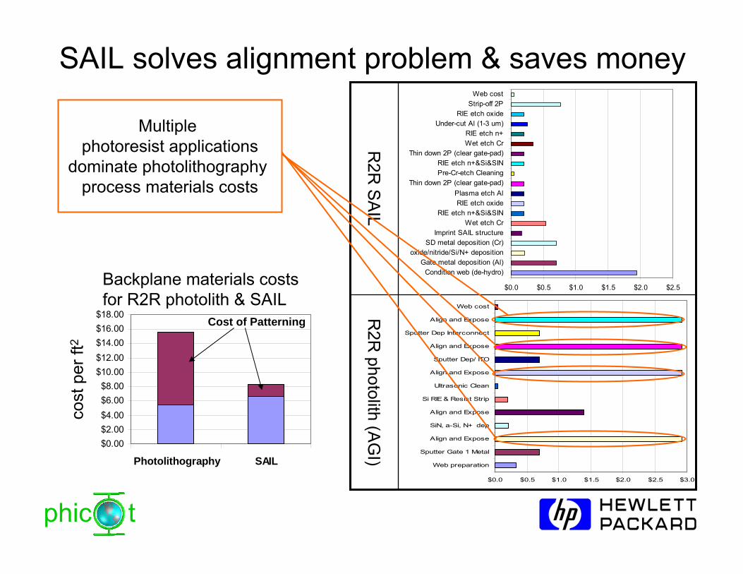
phic t$0.0 $0.5 $1.0 $1.5 $2.0 $2.5 $3.0
Web preparation
Sputter Gate 1 Metal
Align and Expose
SiN, a-Si, N+ dep
Align and Expose
Si RIE & Resist Strip
Ultrasonic Clean
Align and Expose
Sputter Dep/ ITO
Align and Expose
Sputter Dep Interconnect
Align and Expose
Web cost
SAIL solves alignment problem & saves money
$0.0 $0.5 $1.0 $1.5 $2.0 $2.5
Condition web (de-hydro)Gate metal deposition (Al)
PECVD oxide/nitride/Si/N+ depositionSD metal deposition (Cr)
Imprint SAIL structureWet etch Cr
RIE etch n+&Si&SINRIE etch oxide
Plasma etch AlThin down 2P (clear gate-pad)
Pre-Cr-etch CleaningRIE etch n+&Si&SIN
Thin down 2P (clear gate-pad)Wet etch CrRIE etch n+
Under-cut Al (1-3 um)RIE etch oxide
Strip-off 2PWeb cost
cost
per
ft2
$0.00$2.00$4.00$6.00$8.00
$10.00$12.00$14.00$16.00$18.00
Photolithography SAIL
Cost of Patterning
Backplane materials costs for R2R photolith & SAIL
R2R
photolith (AG
I)R
2R S
AIL
Multiple photoresist applications
dominate photolithography process materials costs
phic t
Introduction•What are the key attributes of a paper-like display•Why we need paper-like displays
High Performance Reflective ColorSelf-Aligned Imprint Lithography (SAIL)
• Benefits and challenges of roll-to-roll (R2R) manufacturing• SAIL basics• green manufacturing for green products• toolset for 1/3m wide line• world’s first R2R active matrix displays• ZXO based TFTs for enhanced performance
Outline
phic t
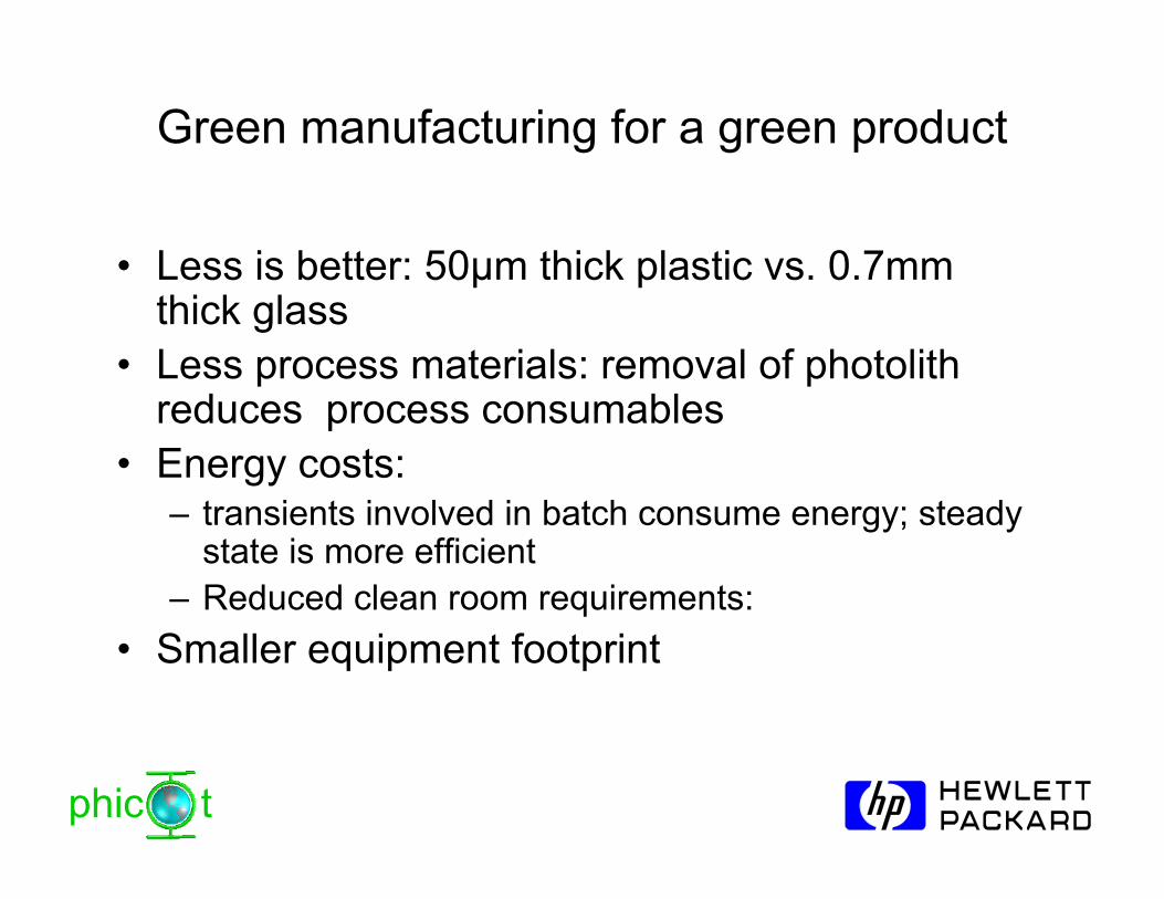
Green manufacturing for a green product
• Less is better: 50μm thick plastic vs. 0.7mm thick glass
• Less process materials: removal of photolith reduces process consumables
• Energy costs: – transients involved in batch consume energy; steady
state is more efficient– Reduced clean room requirements:
• Smaller equipment footprint
phic t
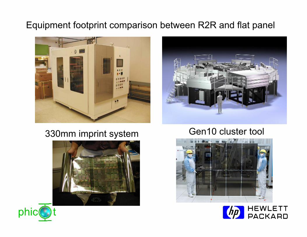
HEPA filter
The web rolled on the core is its own clean room
Ambient Process Vacuum Process
phic t
330mm imprint system Gen10 cluster tool
Equipment footprint comparison between R2R and flat panel
2 3 4 5 6 7 8 9 1010
-3
10-2
10-1
100
equ
ipm
ent c
ost [
M$]
/ th
roug
hput
[cm
2 / S]
generation
equipment cost scaling comparison: panel stepper vs R2R imprinter
100 mm R2R imprinter 330 mm R2R imprinter
Patterning scaling: R2R imprinter compared to panel steppercomparison made at equal throughput
Scaling similar for R2R and panel; cost much lower for R2R
phic t
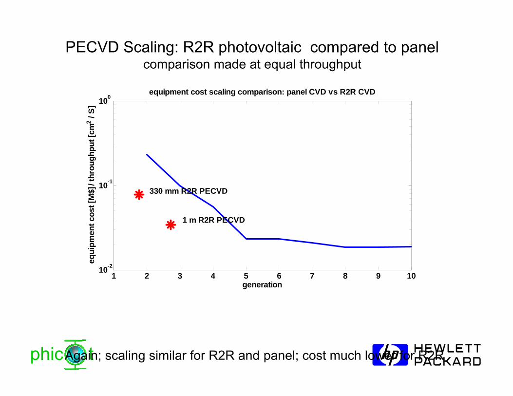
PECVD Scaling: R2R photovoltaic compared to panelcomparison made at equal throughput
Again; scaling similar for R2R and panel; cost much lower for R2R
1 2 3 4 5 6 7 8 9 1010-2
10-1
100 e
quip
men
t cos
t [M
$] /
thro
ughp
ut [c
m2 /
S]
generation
equipment cost scaling comparison: panel CVD vs R2R CVD
330 mm R2R PECVD
1 m R2R PECVD
phic t
Introduction•What are the key attributes of a paper-like display•Why we need paper-like displays
High Performance Reflective ColorSelf-Aligned Imprint Lithography (SAIL)
• Benefits and challenges of roll-to-roll (R2R) manufacturing• SAIL basics• green manufacturing for green products• toolset for 1/3m wide line• world’s first R2R active matrix displays• ZXO based TFTs for enhanced performance
Outline
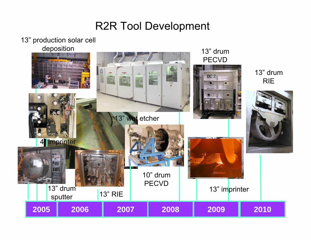
13” production solar cell deposition
4” imprinter
13” RIE13” imprinter
13” drum PECVD
10” drum PECVD
2005 2006 2007 2008 2009 2010
13” wet etcher
13” drum RIE
R2R Tool Development
13” drum sputter
phic t
Web based tools are a lot simpler to build than big panel tools
phic t
Introduction•What are the key attributes of a paper-like display•Why we need paper-like displays
High Performance Reflective ColorSelf-Aligned Imprint Lithography (SAIL)
• Benefits and challenges of roll-to-roll (R2R) manufacturing• SAIL basics• green manufacturing for green products• toolset for 1/3m wide line• world’s first R2R active matrix displays• ZXO based TFTs for enhanced performance
A bubble defect, voids are formed by insufficient volume of photopolymer to fill mold
A crack defect typically results from imbalanced deposition stress
Nonuniform imprinting results in premature mask erosion and feature loss
Tenting defect formed by particle between stamp and substrate at imprinting time or by void in stamp
pinhole defect in metal caused by etchant diffusing through pinhole in oxide
Bridging caused by breakage of imprint stamp in narrow (~2u) regions
phic t
Introduction•What are the key attributes of a paper-like display•Why we need paper-like displays
High Performance Reflective ColorSelf-Aligned Imprint Lithography (SAIL)
• Benefits and challenges of roll-to-roll (R2R) manufacturing• SAIL basics• green manufacturing for green products• toolset for 1/3m wide line• world’s first R2R active matrix displays• ZXO based TFTs for enhanced performance
Outline
phic t
SAIL ZXO TFTs: Motivation, the 3P’s
• Process simplification– Elimination of contact layer removes 2 etch
steps and one deposition step– Huge increase in process margin for critical
channel definition step
• Performance increase– Even with direct metal contacts mobility is
~10X a-Si at the same process temperature– Higher mobility important for emissive pixels
and edge electronics
• Pelucidity (transparency)– Enable see thru displays– Increase aspect ratio for conventional displays
phic t
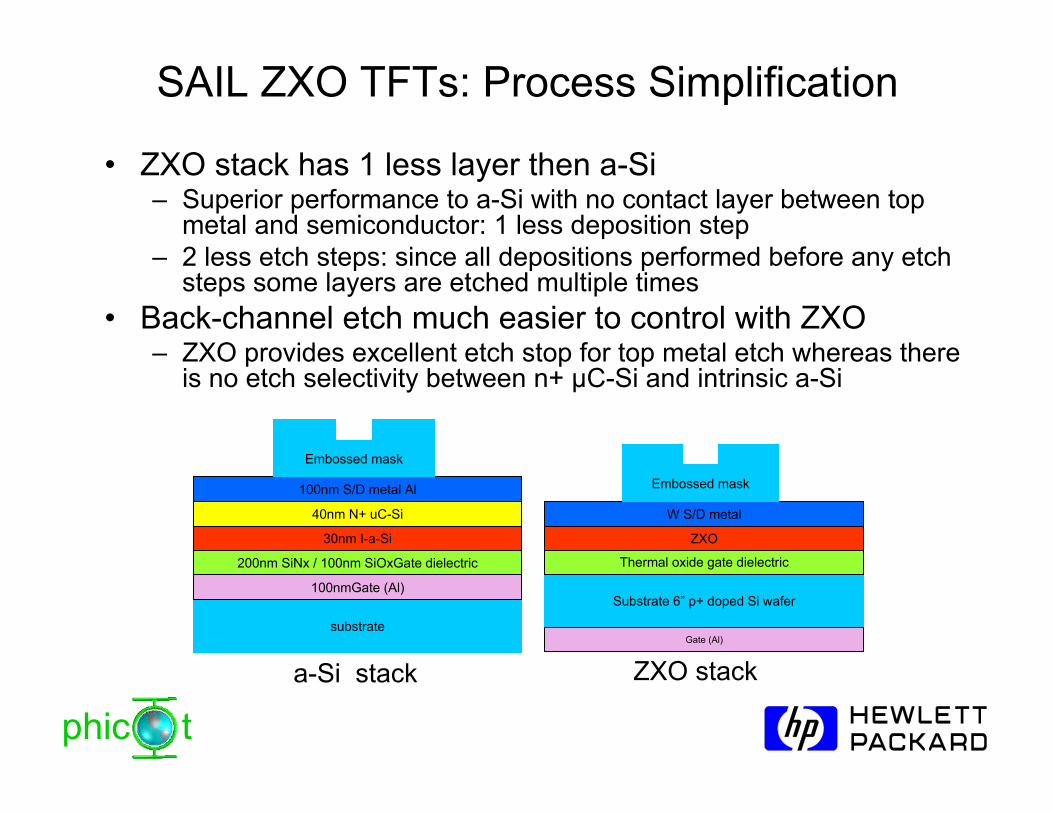
SAIL ZXO TFTs: Process Simplification
• ZXO stack has 1 less layer then a-Si– Superior performance to a-Si with no contact layer between top
metal and semiconductor: 1 less deposition step– 2 less etch steps: since all depositions performed before any etch
steps some layers are etched multiple times• Back-channel etch much easier to control with ZXO
– ZXO provides excellent etch stop for top metal etch whereas there is no etch selectivity between n+ μC-Si and intrinsic a-Si
Substrate 6” p+ doped Si wafer
Gate (Al)
Thermal oxide gate dielectric
ZXO
W S/D metal
Embossed mask
substrate
100nmGate (Al)
200nm SiNx / 100nm SiOxGate dielectric
30nm I-a-Si
40nm N+ uC-Si
100nm S/D metal Al
Embossed mask
a-Si stack ZXO stack
phic t
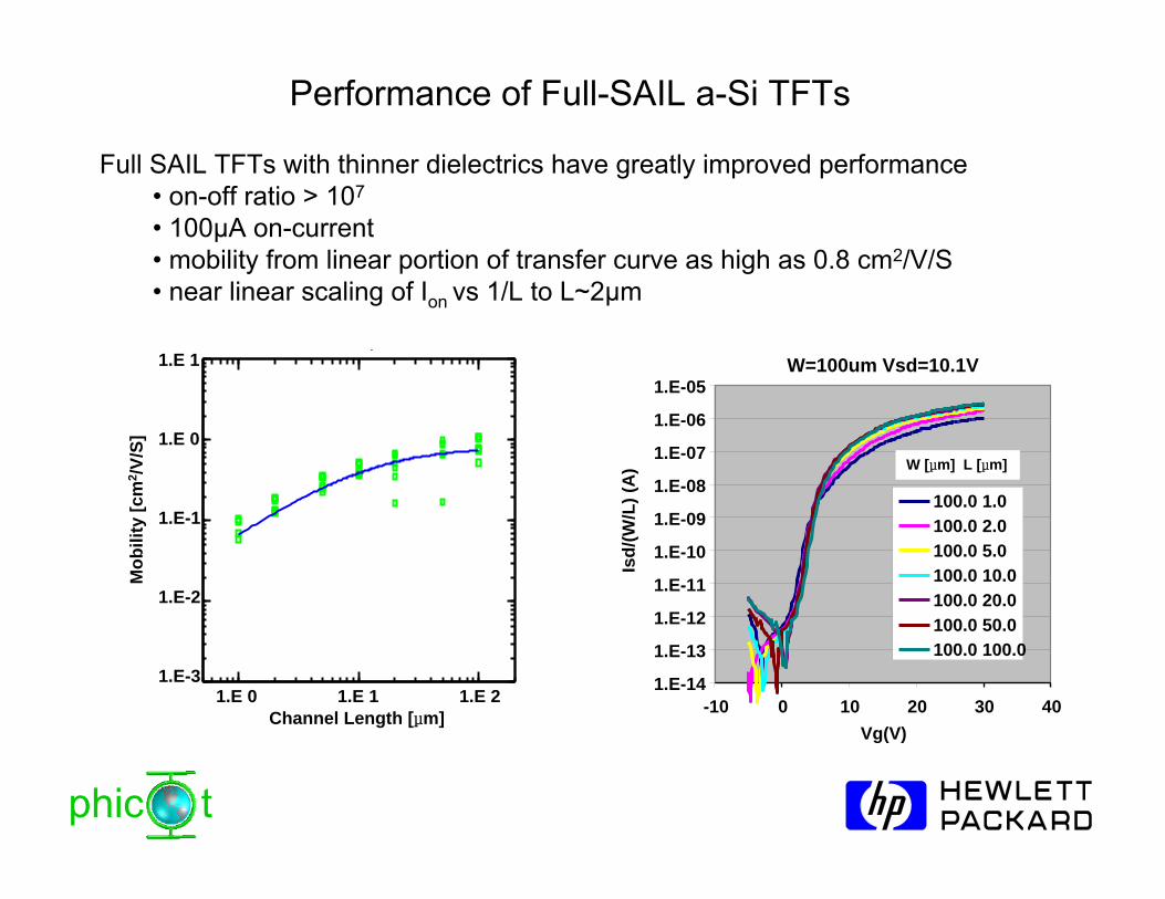
SAIL ZTO TFTs: device measurements
• Mobility strongly dependent on annealing temperature• Performance unrealistically high due to high quality thermal oxide gate dielectric
mobility for 100u long channels vs annealing temperature
0
5
10
15
20
25
200 250 300 350 400
temperature (C)
sat i
ncr m
obili
ty (c
m^2
/V/S
)
Transfer for W=50u, L=50u, Ta=300C
1.E-13
1.E-12
1.E-11
1.E-10
1.E-09
1.E-08
1.E-07
1.E-06
1.E-05
1.E-04
-10 0 10 20 30
Vg (V)
Ids,
Ig (A
)
Id for Vds=10VIg
phic t
Next steps towards commercialization
• September 22, 2008 PowerFilm announced that it has taken a license to the SAIL technology• October 6th, 2008 PowerFilm announced it has won a $1.4M / year cooperative agreement from the U.S. Army for development of a 'self powered flexible display' . HP Labs and PowerFilm will collaborate on the contract.• PowerFilm Solar has created Phicot as a subsidiary to commercialize the technology
phic t
AcknowledgementsThe authors gratefully acknowledge the support of their