CC2510Fx / CC2511Fx SWRS055G Page 1 of 236 Low-Power SoC (System-on-Chip) with MCU, Memory, 2.4 GHz RF Transceiver, and USB Controller Applications • 2400 - 2483.5 MHz ISM/SRD band systems • Consumer electronics • Wireless keyboard and mouse • Wireless voice-quality audio • RF enabled remote controls • Wireless sports and leisure equipment • Low power telemetry • CC2511Fx: USB dongles Product Description The CC2510Fx/CC2511Fx is a true low-cost 2.4 GHz system-on-chip (SoC) designed for low- power wireless applications. The CC2510Fx/CC2511Fx combines the excellent performance of the state-of-the-art RF transceiver CC2500 with an industry-standard enhanced 8051 MCU, up to 32 kB of in-system programmable flash memory and 4 kB of RAM, and many other powerful features. The small 6x6 mm package makes it very suited for applications with size limitations. The CC2510Fx/CC2511Fx is highly suited for systems where very low power consumption is required. This is ensured by several advanced low-power operating modes. The CC2511Fx adds a full-speed USB controller to the feature set of the CC2510Fx. Interfacing to a PC using the USB interface is quick and easy, and the high data rate (12 Mbps) of the USB interface avoids the bottlenecks of RS-232 or low-speed USB interfaces. Key Features • Radio o High-performance RF transceiver based on the market-leading CC2500 o Excellent receiver selectivity and blocking performance o High sensitivity (−103 dBm at 2.4 kBaud) o Programmable data rate up to 500 kBaud o Programmable output power up to 1 dBm for all supported frequencies o Frequency range: 2400 - 2483.5 MHz o Digital RSSI / LQI support • Current Consumption o Low current consumption (RX: 17.1 mA @ 2.4 kBaud, TX: 16 mA @ −6 dBm output power) o 0.3 μA in PM3 (the operating mode with the lowest power consumption) • MCU, Memory, and Peripherals o High performance and low power 8051 microcontroller core. o 8/16/32 kB in-system programmable flash, and 1/2/4 kB RAM o Full-Speed USB Controller with 1 kB USB FIFO (CC2511Fx ) o I 2 S interface o 7 - 12 bit ADC with up to eight inputs o 128-bit AES security coprocessor o Powerful DMA functionality o Two USARTs o 16-bit timer with DSM mode o Three 8-bit timers o Hardware debug support o 21 (CC2510Fx ) or 19 (CC2511Fx ) GPIO pins • General o Wide supply voltage range (2.0V - 3.6V) o Green package: RoHS compliant and no antimony or bromine, 6x6mm QFN 36 CC2511F8 - Not Recommended for New Designs
Transcript
CC2510Fx / CC2511Fx
SWRS055G Page 1 of 236
Low-Power SoC (System-on-Chip) with MCU, Memory, 2.4 GHz RF Transceiver, and USB Controller
Applications • 2400 - 2483.5 MHz ISM/SRD band
systems • Consumer electronics • Wireless keyboard and mouse • Wireless voice-quality audio
• RF enabled remote controls • Wireless sports and leisure equipment • Low power telemetry • CC2511Fx: USB dongles
Product Description
The CC2510Fx/CC2511Fx is a true low-cost 2.4 GHz system-on-chip (SoC) designed for low-power wireless applications. The CC2510Fx/CC2511Fx combines the excellent performance of the state-of-the-art RF transceiver CC2500 with an industry-standard enhanced 8051 MCU, up to 32 kB of in-system programmable flash memory and 4 kB of RAM, and many other powerful features. The small 6x6 mm package makes it very suited for applications with size limitations.
The CC2510Fx/CC2511Fx is highly suited for systems where very low power consumption is required. This is ensured by several advanced low-power operating modes. The CC2511Fx adds a full-speed USB controller to the feature set of the CC2510Fx. Interfacing to a PC using the USB interface is quick and easy, and the high data rate (12 Mbps) of the USB interface avoids the bottlenecks of RS-232 or low-speed USB interfaces.
Key Features
• Radio o High-performance RF transceiver based on
the market-leading CC2500 o Excellent receiver selectivity and blocking
performance o High sensitivity (−103 dBm at 2.4 kBaud) o Programmable data rate up to 500 kBaud o Programmable output power up to 1 dBm for
all supported frequencies o Frequency range: 2400 - 2483.5 MHz o Digital RSSI / LQI support
• Current Consumption o Low current consumption (RX: 17.1 mA @
2.4 kBaud, TX: 16 mA @ −6 dBm output power)
o 0.3 µA in PM3 (the operating mode with the lowest power consumption)
• MCU, Memory, and Peripherals o High performance and low power 8051
microcontroller core. o 8/16/32 kB in-system programmable flash,
and 1/2/4 kB RAM o Full-Speed USB Controller with 1 kB USB
FIFO (CC2511Fx ) o I2S interface o 7 - 12 bit ADC with up to eight inputs o 128-bit AES security coprocessor o Powerful DMA functionality o Two USARTs o 16-bit timer with DSM mode o Three 8-bit timers o Hardware debug support o 21 (CC2510Fx ) or 19 (CC2511Fx ) GPIO pins
• General o Wide supply voltage range (2.0V - 3.6V) o Green package: RoHS compliant and no
antimony or bromine, 6x6mm QFN 36
CC2511F8 - Not Recommended for New Designs
CC2510Fx / CC2511Fx
SWRS055G Page 2 of 236
Table of Contents
ABBREVIATIONS ................................................................................................................................................ 4 1 REGISTER CONVENTIONS .................................................................................................................. 5 2 KEY FEATURES (IN MORE DETAILS) .............................................................................................. 6 2.1 HIGH-PERFORMANCE AND LOW-POWER 8051-COMPATIBLE MICROCONTROLLER....................................... 6 2.2 8/16/32 KB NON-VOLATILE PROGRAM MEMORY AND 1/2/4 KB DATA MEMORY ......................................... 6 2.3 FULL-SPEED USB CONTROLLER (CC2511FX ) ............................................................................................... 6 2.4 I2S INTERFACE .............................................................................................................................................. 6 2.5 HARDWARE AES ENCRYPTION/DECRYPTION ............................................................................................... 6 2.6 PERIPHERAL FEATURES ................................................................................................................................ 6 2.7 LOW POWER ................................................................................................................................................. 6 2.8 2.4 GHZ RADIO WITH BASEBAND MODEM ................................................................................................... 7 3 ABSOLUTE MAXIMUM RATINGS ...................................................................................................... 8 4 OPERATING CONDITIONS .................................................................................................................. 9 4.1 CC2510FX OPERATING CONDITIONS .............................................................................................................. 9 4.2 CC2511FX OPERATING CONDITIONS .............................................................................................................. 9 5 GENERAL CHARACTERISTICS .......................................................................................................... 9 6 ELECTRICAL SPECIFICATIONS ...................................................................................................... 10 6.1 CURRENT CONSUMPTION ........................................................................................................................... 10 6.2 RF RECEIVE SECTION ................................................................................................................................. 13 6.3 RF TRANSMIT SECTION .............................................................................................................................. 15 6.4 CRYSTAL OSCILLATORS ............................................................................................................................. 16 6.5 32.768 KHZ CRYSTAL OSCILLATOR ........................................................................................................... 17 6.6 LOW POWER RC OSCILLATOR .................................................................................................................... 17 6.7 HIGH SPEED RC OSCILLATOR .................................................................................................................... 18 6.8 FREQUENCY SYNTHESIZER CHARACTERISTICS ........................................................................................... 18 6.9 ANALOG TEMPERATURE SENSOR ............................................................................................................... 19 6.10 7 - 12 BIT ADC ........................................................................................................................................... 20 6.11 CONTROL AC CHARACTERISTICS ............................................................................................................... 22 6.12 SPI AC CHARACTERISTICS ......................................................................................................................... 23 6.13 DEBUG INTERFACE AC CHARACTERISTICS ................................................................................................ 24 6.14 PORT OUTPUTS AC CHARACTERISTICS ...................................................................................................... 24 6.15 TIMER INPUTS AC CHARACTERISTICS ........................................................................................................ 25 6.16 DC CHARACTERISTICS ............................................................................................................................... 25 7 PIN AND I/O PORT CONFIGURATION ............................................................................................ 26 8 CIRCUIT DESCRIPTION ..................................................................................................................... 30 8.1 CPU AND PERIPHERALS ............................................................................................................................. 31 8.2 RADIO ........................................................................................................................................................ 33 9 APPLICATION CIRCUIT ..................................................................................................................... 33 9.1 BIAS RESISTOR ........................................................................................................................................... 33 9.2 BALUN AND RF MATCHING ........................................................................................................................ 33 9.3 CRYSTAL .................................................................................................................................................... 33 9.4 REFERENCE SIGNAL ................................................................................................................................... 34 9.5 USB (CC2511FX) ......................................................................................................................................... 34 9.6 POWER SUPPLY DECOUPLING ..................................................................................................................... 34 9.7 PCB LAYOUT RECOMMENDATIONS ............................................................................................................ 38 10 8051 CPU .................................................................................................................................................. 39 10.1 8051 INTRODUCTION .................................................................................................................................. 39 10.2 MEMORY .................................................................................................................................................... 39 10.3 CPU REGISTERS ......................................................................................................................................... 51 10.4 INSTRUCTION SET SUMMARY ..................................................................................................................... 53 10.5 INTERRUPTS ................................................................................................................................................ 57 11 DEBUG INTERFACE ............................................................................................................................. 68 11.1 DEBUG MODE ............................................................................................................................................. 68 11.2 DEBUG COMMUNICATION........................................................................................................................... 68 11.3 DEBUG LOCK BIT ....................................................................................................................................... 68
CC2511F8 - Not Recommended for New Designs
CC2510Fx / CC2511Fx
SWRS055G Page 3 of 236
11.4 DEBUG COMMANDS.................................................................................................................................... 69 12 PERIPHERALS ....................................................................................................................................... 73 12.1 POWER MANAGEMENT AND CLOCKS.......................................................................................................... 73 12.2 RESET ......................................................................................................................................................... 80 12.3 FLASH CONTROLLER .................................................................................................................................. 81 12.4 I/O PORTS ................................................................................................................................................... 87 12.5 DMA CONTROLLER ................................................................................................................................... 98 12.6 16-BIT TIMER, TIMER 1 ............................................................................................................................. 109 12.7 MAC TIMER (TIMER 2) ............................................................................................................................ 121 12.8 SLEEP TIMER ............................................................................................................................................ 123 12.9 8-BIT TIMERS, TIMER 3 AND TIMER 4 ....................................................................................................... 126 12.10 ADC ......................................................................................................................................................... 137 12.11 RANDOM NUMBER GENERATOR ............................................................................................................... 143 12.12 AES COPROCESSOR .................................................................................................................................. 144 12.13 WATCHDOG TIMER ................................................................................................................................... 147 12.14 USART .................................................................................................................................................... 149 12.15 I2S ............................................................................................................................................................ 159 12.16 USB CONTROLLER ................................................................................................................................... 167 13 RADIO .................................................................................................................................................... 183 13.1 COMMAND STROBES ................................................................................................................................ 183 13.2 RADIO REGISTERS .................................................................................................................................... 185 13.3 INTERRUPTS .............................................................................................................................................. 185 13.4 TX/RX DATA TRANSFER ......................................................................................................................... 187 13.5 DATA RATE PROGRAMMING ..................................................................................................................... 188 13.6 RECEIVER CHANNEL FILTER BANDWIDTH ................................................................................................ 188 13.7 DEMODULATOR, SYMBOL SYNCHRONIZER, AND DATA DECISION ............................................................ 189 13.8 PACKET HANDLING HARDWARE SUPPORT ............................................................................................... 190 13.9 MODULATION FORMATS ........................................................................................................................... 193 13.10 RECEIVED SIGNAL QUALIFIERS AND LINK QUALITY INFORMATION ......................................................... 194 13.11 FORWARD ERROR CORRECTION WITH INTERLEAVING .............................................................................. 197 13.12 RADIO CONTROL ...................................................................................................................................... 198 13.13 FREQUENCY PROGRAMMING .................................................................................................................... 201 13.14 VCO ......................................................................................................................................................... 202 13.15 OUTPUT POWER PROGRAMMING .............................................................................................................. 202 13.16 SELECTIVITY ............................................................................................................................................ 203 13.17 SYSTEM CONSIDERATIONS AND GUIDELINES ........................................................................................... 205 13.18 RADIO REGISTERS .................................................................................................................................... 208 14 VOLTAGE REGULATORS ................................................................................................................ 226 14.1 VOLTAGE REGULATOR POWER-ON ........................................................................................................... 226 15 RADIO TEST OUTPUT SIGNALS ..................................................................................................... 226 16 REGISTER OVERVIEW ..................................................................................................................... 228 17 REFERENCES ...................................................................................................................................... 232 18 GENERAL INFORMATION ............................................................................................................... 233 18.1 DOCUMENT HISTORY ............................................................................................................................... 233
CC2511F8 - Not Recommended for New Designs
CC2510Fx / CC2511Fx
SWRS055G Page 4 of 236
Abbreviations
∆Σ Delta-Sigma ADC Analog to Digital Converter AES Advanced Encryption Standard AGC Automatic Gain Control ARIB Association of Radio Industries and
Businesses BCD Binary Coded Decimal BER Bit Error Rate BOD Brown Out Detector CBC Cipher Block Chaining CBC-MAC
Cipher Block Chaining Message Authentication Code
CCA Clear Channel Assessment CCM Counter mode + CBC-MAC CFB Cipher Feedback CFR Code of Federal Regulations CMOS Complementary Metal Oxide
Semiconductor CPU Central Processing Unit CRC Cyclic Redundancy Check CTR Counter mode (encryption) DAC Digital to Analog Converter DMA Direct Memory Access DSM Delta-Sigma Modulator ECB Electronic Code Book EM Evaluation Module ENOB Effective Number of Bits EP0 - 5 USB Endpoints 0 - 5 ESD Electro Static Discharge ESR Equivalent Series Resistance ETSI European Telecommunications Standard
Institute FCC Federal Communications Commission FIFO First In First Out GPIO General Purpose Input / Output HSSD High Speed Serial Debug HW Hardware I2S Inter-IC Sound I/O Input / Output I/Q In-phase / Quadrature-phase IF Intermediate Frequency IOC I/O Controller ISM Industrial, Scientific and Medical ISR Interrupt Service Routine IV Initialization Vector JEDEC Joint Electron Device Engineering Council kbps kilo bits per second KB Kilo Bytes (1024 bytes) LFSR Linear Feedback Shift Register
LNA Low-Noise Amplifier LO Local Oscillator LQI Link Quality Indication LSB Least Significant Bit / Byte MAC Medium Access Control MCU Microcontroller Unit MISO Master In Slave Out MOSI Master Out Slave In MSB Most Significant Bit / Byte NA Not Applicable OFB Output Feedback (encryption) PA Power Amplifier PCB Printed Circuit Board PER Packet Error Rate PLL Phase Locked Loop PM0 - 3 Power Mode 0 - 3 PMC Power Management Controller POR Power On Reset PWM Pulse Width Modulator Px_n Port x pin n (x = 0, 1, or 2 and
n = 0, 1, 2, .., 7) QLP Quad Leadless Package RAM Random Access Memory RCOSC RC Oscillator RF Radio Frequency RoHS Restriction on Hazardous Substances RSSI Receive Signal Strength Indicator RX Receive SCK Serial Clock SFD Start of Frame Delimiter SFR Special Function Register SINAD Signal-to-noise and distortion ratio SPI Serial Peripheral Interface SRAM Static Random Access Memory SW Software T/R Transmit / Receive TX Transmit UART Universal Asynchronous
Receiver/Transmitter USB Universal Serial Bus VCO Voltage Controlled Oscillator VGA Variable Gain Amplifier WDT Watchdog Timer XOSC Crystal Oscillator
CC2511F8 - Not Recommended for New Designs
CC2510Fx / CC2511Fx
SWRS055G Page 5 of 236
1 Register Conventions
Each SFR is described in a separate table. The table heading is given in the following format:
REGISTER NAME (SFR Address) - Register Description.
Each RF register is described in a separate table. The table heading is given in the following format:
XDATA Address: REGISTER NAME - Register Description
All register descriptions include a symbol denoted R/W describing the accessibility of each bit in the register. The register values are always given in binary notation unless prefixed by ‘0x’, which indicates hexadecimal notation.
Symbol Access Mode
R/W Read/write
R Read only
R0 Read as 0
R1 Read as 1
W Write only
W0 Write as 0
W1 Write as 1
H0 Hardware clear
H1 Hardware set
Table 1: Register Bit Conventions
CC2511F8 - Not Recommended for New Designs
CC2510Fx / CC2511Fx
SWRS055G Page 6 of 236
2 Key Features (in more details) 2.1 High-Performance and Low-Power
8051-Compatible Microcontroller
• Optimized 8051 core which typically gives 8x the performance of a standard 8051
• Two data pointers
• In-circuit interactive debugging is supported by the IAR Embedded Workbench through a simple two-wire serial interface
• SW compatible with CC1110Fx/CC1111Fx
2.2 8/16/32 kB Non-volatile Program Memory and 1/2/4 kB Data Memory
• 8, 16, or 32 kB of non-volatile flash memory, in-system programmable through a simple two-wire interface or by the 8051 core
• Programmable read and write lock of portions of flash memory for software security
• 1, 2, or 4 kB of internal SRAM
2.3 Full-Speed USB Controller (CC2511Fx )
• 5 bi-directional endpoints in addition to control endpoint 0
• Full-Speed, 12 Mbps transfer rate
• Support for Bulk, Interrupt, and Isochronous endpoints
• 1024 bytes of dedicated endpoint FIFO memory
• 8 - 512 byte data packet size supported
• Configurable FIFO size for IN and OUT direction of endpoint
2.4 I2S Interface
• Industry standard I2S interface for transfer of digital audio data
• Full duplex
• Mono and stereo support
• Configurable sample rate and sample size
• Support for µ-law compression and expansion
• Typically used to connect to external DAC or ADC
2.5 Hardware AES Encryption/Decryption
• 128-bit AES supported in hardware coprocessor
2.6 Peripheral Features
• Powerful DMA Controller
• Power On Reset/Brown-Out Detection
• ADC with eight individual input channels, single-ended or differential (CC2511Fx has six channels) and configurable resolution
• Programmable watchdog timer
• Five timers: one general 16-bit timer with DSM mode, two general 8-bit timers, one MAC timer, and one sleep timer
• Two programmable USARTs for master/slave SPI or UART operation
• 21 configurable general-purpose digital I/O-pins (CC2511Fx has 19)
• Random number generator
2.7 Low Power
• Four flexible power modes for reduced power consumption
• System can wake up on external interrupt or when the Sleep Timer expires
• 0.5 µA current consumption in PM2, where external interrupts or the Sleep Timer can wake up the system
• 0.3 µA current consumption in PM3, where external interrupts can wake up the system
• Low-power fully static CMOS design
• System clock source is either a high speed crystal oscillator (24 - 27 MHz for CC2510Fx and 48 MHz for CC2511Fx) or a high speed RC oscillator (12 - 13.5 MHz for CC2510Fx and 12 MHz for CC2511Fx).
CC2511F8 - Not Recommended for New Designs
CC2510Fx / CC2511Fx
SWRS055G Page 7 of 236
The high speed crystal oscillator must be used when the radio is active.
• Clock source for ultra-low power operation can be either a low-power RC oscillator or an optional 32.768 kHz crystal oscillator
• Very fast transition to active mode from power modes enables ultra low average power consumption in low duty-cycle systems
2.8 2.4 GHz Radio with Baseband Modem
• Based on the industry leading CC2500 radio core
• Few external components: On-chip frequency synthesizer, no external filters or RF switch needed
• Flexible support for packet oriented systems: On-chip support for sync word detection, address check, flexible packet length, and automatic CRC handling
• Supports use of DMA for both RX and TX resulting in minimal CPU intervention even on high data rates
• Programmable channel filter bandwidth
• 2-FSK, GFSK and MSK supported
• Optional automatic whitening and de-whitening of data
• Programmable Carrier Sense (CS) indicator
• Programmable Preamble Quality Indicator for detecting preambles and improved protection against sync word detection in random noise
• Support for automatic Clear Channel Assessment (CCA) before transmitting (for listen-before-talk systems
• Support for per-package Link Quality Indication (LQI)
• Suited for systems targeting compliance with EN 300 328, EN 300 440, FCC CFR47 Part 15 and ARIB STD-T-66
• When transmitting in band 2480 - 2483.5 MHz under FCC, duty-cycling or reducing output power might be needed
CC2511F8 - Not Recommended for New Designs
CC2510Fx / CC2511Fx
SWRS055G Page 8 of 236
3 Absolute Maximum Ratings
Under no circumstances must the absolute maximum ratings given in Table 2 be violated. Stress exceeding one or more of the limiting values may cause permanent damage to the device.
Parameter Min Max Units Condition
Supply voltage (VDD) −0.3 3.9 V All supply pins must have the same voltage
Voltage on any digital pin −0.3 VDD + 0.3, max 3.9
V
Voltage on the pins RF_P, RF_N and DCOUPL
−0.3 2.0 V
Voltage ramp-up rate 120 kV/µs
Input RF level 10 dBm
Storage temperature range −50 150 °C Device not programmed
Solder reflow temperature 260 °C According to IPC/JEDEC J-STD-020D
ESD CC2510Fx 750 V According to JEDEC STD 22, method A114, Human Body Model (HBM)
ESD CC2510Fx 500 V According to JEDEC STD 22, C101C, Charged Device Model (CDM)
ESD CC2511x 750 V According to JEDEC STD 22, method A114, Human Body Model (HBM)
ESD CC2511x 500 V According to JEDEC STD 22, C101C, Charged Device Model (CDM)
Table 2: Absolute Maximum Ratings
Caution! ESD sensitive device. Precaution should be used when handling the device in order to prevent permanent damage.
CC2511F8 - Not Recommended for New Designs
CC2510Fx / CC2511Fx
SWRS055G Page 9 of 236
4 Operating Conditions
4.1 CC2510Fx Operating Conditions
The operating conditions for CC2510Fx are listed in Table 3 below.
Parameter Min Max Unit Condition
Operating ambient temperature, TA −40 85 °C
Operating supply voltage (VDD) 2.0 3.6 V All supply pins must have the same voltage
Table 3: Operating Conditions for CC2510Fx
4.2 CC2511Fx Operating Conditions
The operating conditions for CC2511Fx are listed in Table 4 below.
Parameter Min Max Unit Condition
Operating ambient temperature, TA 0 85 °C
Operating supply voltage (VDD) 3.0 3.6 V All supply pins must have the same voltage
Table 4: Operating Conditions for CC2511Fx
5 General Characteristics
TA = 25°C, VDD = 3.0 V if nothing else stated
Parameter Min Typ Max Unit Condition/Note
Radio part
Frequency range 2400 2483.5 MHz There will be spurious signals at n/2·crystal oscillator frequency (n is an integer number). RF frequencies at n/2·crystal oscillator frequency should therefore be avoided (e.g. 2405, 2418, 2431, 2444, 2457, 2470 and 2483 MHz when using a 26 MHz crystal).
Data rate 1.2
1.2
26
500
250
500
kBaud
kBaud
kBaud
2-FSK
GFSK
(Shaped) MSK (also known as differential offset QPSK)
Optional Manchester encoding (the data rate in kbps will be half the baud rate)
Wake-Up Timing
PM1 Active Mode
4 µs Digital regulator on. HS RCOSC and high speed crystal oscillator off. 32.768 kHz XOSC or low power RCOSC running.
SLEEP.OSC_PD=1 and CLKCON.OSC=1
PM2/3 Active Mode
100 µs Digital regulator off. HS RCOSC and high speed crystal oscillator off. 32.768 kHz XOSC or low power RCOSC running (PM2). No crystal oscillators or RC oscillators are running in PM3.
SLEEP.OSC_PD=1 and CLKCON.OSC=1
Table 5: General Characteristics
CC2511F8 - Not Recommended for New Designs
CC2510Fx / CC2511Fx
SWRS055G Page 10 of 236
6 Electrical Specifications
6.1 Current Consumption
TA = 25°C, VDD = 3.0 V if nothing else stated. All measurement results are obtained using the CC2510EM reference design ([1]). Parameter Min Typ Max Unit Condition
Active mode, full speed (high speed crystal oscillator)1.
Low CPU activity.
4.8 mA System clock running at 26 MHz.
4.6 mA System clock running at 24 MHz.
Digital regulator on. High speed crystal oscillator and low power RCOSC running. No peripherals running. Low CPU activity: No flash access (i.e. only cache hit), no RAM access
Active mode, full speed (HS RCOSC)1. Low CPU activity.
2.5 mA System clock running at 13 MHz. Digital regulator on. HS RCOSC and low power RCOSC running. No peripherals running. Low CPU activity: No flash access (i.e. only cache hit), no RAM access
Active mode with radio in RX
Digital regulator on. High speed crystal oscillator and low power RCOSC running. Radio in RX mode (sensitivity optimized MDMCFG2.DEM_DCFILT_OFF=0)
19.8
20.6
17.1
mA
mA
mA
2.4 kBaud, input at sensitivity limit, system clock running at 26 MHz.
2.4 kBaud, input at sensitivity limit, system clock running at 24 MHz.
2.4 kBaud, input at sensitivity limit, system clock running at 203 kHz.
19.8 mA 2.4 kBaud, input well above sensitivity limit, system clock running at 26 MHz.
21.5
22.1
18.8
mA
mA
mA
10 kBaud, input at sensitivity limit, system clock running at 26 MHz.
10 kBaud, input at sensitivity limit, system clock running at 24 MHz.
10 kBaud, input at sensitivity limit, system clock running at 203 kHz.
19.0 mA 10 kBaud, input well above sensitivity limit, system clock running at 26 MHz.
22.9
22.7
20.5
mA
mA
mA
250 kBaud, input at sensitivity limit, system clock running at 26 MHz.
250 kBaud, input at sensitivity limit, system clock running at 24 MHz.
250 kBaud, input at sensitivity limit, system clock running at 1.625 MHz.
19.6 mA 250 kBaud, input well above sensitivity limit, system clock running at 26 MHz. See Figure 2 for typical variation over operating conditions
19.7
20.8
17.5
mA
mA
mA
500 kBaud, input at sensitivity limit, system clock running at 26 MHz.
500 kBaud, input at sensitivity limit, system clock running at 24 MHz.
500 kBaud, input at sensitivity limit, system clock running at 3.25 MHz.
16.7 mA 500 kBaud, input well above sensitivity limit
Digital regulator on. High speed crystal oscillator and low power RCOSC running. Radio in RX mode (current optimized MDMCFG2.DEM_DCFILT_OFF=1)
17.4 mA 2.4 kBaud, input at sensitivity limit, system clock running at 26 MHz.
14.7 mA 2.4 kBaud, input at sensitivity limit, system clock running at 203 kHz.
17.4 mA 2.4 kBaud, input well above sensitivity limit, system clock running at 26 MHz.
1 Note: In order to reduce the current consumption in active mode, the clock speed can be reduced by setting CLKCON.CLKSPD≠000 (see section 13.1 for details). Figure 1 shows typical current consumption in active mode for different clock speeds
CC2511F8 - Not Recommended for New Designs
CC2510Fx / CC2511Fx
SWRS055G Page 11 of 236
Parameter Min Typ Max Unit Condition
19.4 mA 10 kBaud, input at sensitivity limit, system clock running at 26 MHz.
15.7 mA 10 kBaud, input at sensitivity limit, system clock running at 203 kHz.
16.9 mA 10 kBaud, input well above sensitivity limit, system clock running at 26 MHz.
Active mode with radio in TX
System clock running at 26 MHz.
Digital regulator on. High speed crystal oscillator and low power RCOSC running. Radio in TX mode
26 mA 0 dBm output power (PA_TABLE0=0xFE). See Table 7 for typical variation over operating conditions
18.5 mA −6 dBm output power (PA_TABLE0=0x7F)
15.5 mA −12 dBm output power (PA_TABLE0=0x95)
26 mA System clock running at 24 MHz.
Digital regulator on. High speed crystal oscillator and low power RCOSC running. Radio in TX mode w/0 dBm output power (PA_TABLE0=0xFE)
PM0 4.3 mA Same as active mode, but the CPU is not running (see 12.1.2.2 for details). System clock running at 26 MHz
PM1 220 µA Digital regulator on. HS RCOSC and high speed crystal oscillator off. 32.768 kHz XOSC or low power RCOSC running (see 12.1.2.3 for details)
PM2 0.5 1 µA Digital regulator off. HS RCOSC and high speed crystal oscillator off. Low power RCOSC running (see 12.1.2.4 for details)
PM3 0.3 1 µA Digital regulator off. No crystal oscillators or RC oscillators are running (see 12.1.2.5 for details)
Peripheral Current Consumption
Add to the figures above if the peripheral unit is activated
Timer 1 2.7 µA/MHz When running
Timer 2 1.3 µA/MHz When running
Timer 3 1.6 µA/MHz When running
Timer 4 2 µA/MHz When running
ADC 1.2 mA During conversion
Table 6: Current Consumption
CC2511F8 - Not Recommended for New Designs
CC2510Fx / CC2511Fx
SWRS055G Page 12 of 236
Figure 1: Current Consumption (Active Mode) vs. Clock Speed
Figure 2: Typical Variation in RX Current Consumption over Temperature and Input Power Level. Data Rate = 250 kBaud.
Supply Voltage, VDD = 2 V Supply Voltage, VDD = 3 V Supply Voltage, VDD = 3.6 V
−103 dBm The RX current consumption can be reduced by approximately 2.4 mA by setting MDMCFG2.DEM_DCFILT_OFF=1. The typical sensitivity is then −101 dBm.
The sensitivity can be improved to typically −105 dBm with MDMCFG2.DEM_DCFILT_OFF=0 by changing registers TEST2 and TEST1 (see Page 222). The temperature range is then from 0oC to 85oC.
Saturation −10 dBm
Adjacent channel rejection
23 dB Desired channel 3 dB above the sensitivity limit. 250 kHz channel spacing
Alternate channel rejection
32 dB Desired channel 3 dB above the sensitivity limit. 250 kHz channel spacing
See Figure 55 for plot of selectivity versus frequency offset
−98 dBm The RX current consumption can be reduced by approximately 2.2 mA by setting MDMCFG2.DEM_DCFILT_OFF=1. The typical sensitivity is then −97 dBm.
The sensitivity can be improved to typically −100 dBm with MDMCFG2.DEM_DCFILT_OFF=0 by changing registers TEST2 and TEST1 (see Page 222). The temperature range is then from 0oC to 85oC.
Saturation −9 dBm
Adjacent channel rejection
19 dB Desired channel 3 dB above the sensitivity limit. 250 kHz channel spacing
Alternate channel rejection
25 dB Desired channel 3 dB above the sensitivity limit. 250 kHz channel spacing
See Figure 56 for plot of selectivity versus frequency offset
Table 9: Typical Variation in Sensitivity over Temperature and Supply Voltage @ 2.44 GHz and 250 kBaud Data Rate
CC2511F8 - Not Recommended for New Designs
CC2510Fx / CC2511Fx
SWRS055G Page 15 of 236
6.3 RF Transmit Section
TA = 25°C, VDD = 3.0 V if nothing else stated. All measurement results are obtained using the CC2510EM reference designs ([1]).
Parameter Min Typ Max Unit Condition/Note
Differential load impedance
80 + j74 Ω Differential impedance as seen from the RF-port (RF_P and RF_N) towards the antenna. Follow the CC2510EM reference design [1] available from TI’s website.
Output power, highest setting
1 dBm Output power is programmable and is available across the entire frequency band. See Figure 3 typical variation over operating conditions (output power is 0 dBm)
Delivered to a 50 Ω single-ended load via the CC2510EM reference design [1] RF matching network.
Output power, lowest setting
−30 dBm Output power is programmable and is available across the entire frequency band
Delivered to a 50 Ω single-ended load via the CC2510EM reference design [1] RF matching network.
Crystal frequency 24 26 27 MHz Referred to as fXOSC. For operation below 26 MHz, please refer to Table 4 for Operating Conditions.
Crystal frequency accuracy requirement
±40 ppm This is the total tolerance including a) initial tolerance, b) crystal loading, c) aging, and d) temperature dependence.
The acceptable crystal tolerance depends on RF frequency and channel spacing / bandwidth.
C0 1 5 7 pF Simulated over operating conditions
Load capacitance 10 13 20 pF Simulated over operating conditions
ESR 100 Ω Simulated over operating conditions
Start-up time 250 μs fXOSC = 26 MHz
Note: A Ripple counter of 12 bit is included to ensure duty-cycle requirements. Start-up time includes ripple counter delay until SLEEP.XOSC_STB is asserted
Power Down Guard Time
3 ms The crystal oscillator must be in power down for a guard time before it is used again. This requirement is valid for all modes of operation. The need for power down guard time can vary with crystal type and load. Minimum figure is valid for reference crystal NDK, AT-41CD2 and load capacitance according to Table 29.
If power down guard time is violated, one of the consequences can be increased PER when using the radio immediately after the crystal oscillator has been reported stable.
Table 11: CC2510Fx Crystal Oscillator Parameters
6.4.2 CC2511Fx Crystal Oscillator
TA = 25°C, VDD = 3.0 V if nothing else is stated.
Parameter Min Typ Max Unit Condition/Note
Crystal frequency 48 MHz Referred to as fXOSC
Crystal frequency accuracy requirement
±40 ppm This is the total tolerance including a) initial tolerance, b) crystal loading, c) aging, and d) temperature dependence.
The acceptable crystal tolerance depends on RF frequency and channel spacing / bandwidth.
C0
Fundamental 0.85 1 1.15 pF Simulated over operating conditions. Variation given by reference crystal NX2520SA from NDK
3rd overtone 2 3 7 pF
Load capacitance 15 16 17 pF Simulated over operating conditions
ESR 60 Ω Simulated over operating conditions
Start-up time Note: A Ripple counter of 14 bit is included to ensure duty-cycle requirements. Start-up time includes ripple counter delay until SLEEP.XOSC_STB is asserted
Fundamental 650 μs
3rd overtone 3 ms Simulated value
Table 12: CC2511Fx Crystal Oscillator Parameters
CC2511F8 - Not Recommended for New Designs
CC2510Fx / CC2511Fx
SWRS055G Page 17 of 236
6.5 32.768 kHz Crystal Oscillator
TA = 25°C, VDD = 3.0V if nothing else is stated.
Parameter Min Typ Max Unit Condition/Note
Crystal frequency 32.768 kHz
C0 0.9 2.0 pF Simulated over operating conditions
Load capacitance 12 16 pF Simulated over operating conditions
kHz CC2510Fx CC2511Fx Calibrated low power RC oscillator frequency is fRef / 750
Frequency accuracy after calibration
±1 %
Temperature coefficient +0.5 %/°C Frequency drift when temperature changes after calibration
Supply voltage coefficient +3 %/V Frequency drift when supply voltage changes after calibration
Initial calibration time 2 ms When the low power RC oscillator is enabled, calibration is continuously done in the background as long as the high speed crystal oscillator is running.
Table 14: Low Power RC Oscillator Parameters
2 fRef = fXOSC for CC2510Fx and fRef = fXOSC /2 for CC2511Fx For CC2510Fx Min figures are given using fXOSC = 24 MHz. Typ figures are given using fXOSC = 26 MHz, and Max figures are given using fXOSC = 27 MHz. For CC2511Fx, fXOSC = 48 MHz
CC2511F8 - Not Recommended for New Designs
CC2510Fx / CC2511Fx
SWRS055G Page 18 of 236
6.7 High Speed RC Oscillator
TA = 25°C, VDD = 3.0 V if nothing else is stated.
Parameter Min Typ Max Unit Condition/Note
Calibrated frequency2 12 13 13.5 MHz Calibrated HS RCOSC frequency is fXOSC / 2
Uncalibrated frequency accuracy
±15 %
Calibrated frequency accuracy
±1 %
Start-up time 10 µs
Temperature coefficient −325 ppm/°C Frequency drift when temperature changes after calibration
Supply voltage coefficient
28 ppm/V Frequency drift when supply voltage changes after calibration
Calibration time 65 µs The HS RCOSC will be calibrated once when the high speed crystal oscillator is selected as system clock source (CLKCON.OSC is set to 0), and also when the system wakes up from PM1 - 3 if CLKCON.OSC was set to 0 when entering PM1 - 3. See 12.1.5.1 for details).
Table 15: High Speed RC Oscillator Parameters
6.8 Frequency Synthesizer Characteristics
TA = 25°C, VDD = 3.0 V if nothing else stated. All measurement results are obtained using the CC2510EM reference designs ([1]).
Parameter Min Typ Max Unit Condition/Note
Programmed frequency resolution3
366
366
397
366
412
366
Hz CC2510Fx CC2511Fx Frequency resolution = fRef/ 216
Synthesizer frequency tolerance
±40 ppm Given by crystal used. Required accuracy (including temperature and aging) depends on frequency band and channel bandwidth / spacing.
3 fRef = fXOSC for CC2510Fx and fRef = fXOSC /2 for CC2511Fx For CC2510Fx Min figures are given using fXOSC = 24 MHz. Typ figures are given using fXOSC = 26 MHz, and Max figures are given using fXOSC = 27 MHz. For CC2511Fx, fXOSC = 48 MHz
CC2511F8 - Not Recommended for New Designs
CC2510Fx / CC2511Fx
SWRS055G Page 19 of 236
Parameter Min Typ Max Unit Condition/Note
PLL turn-on / hop time4 72.4
81.4
75.2
81.4
81.4
81.4
µs CC2510Fx CC2511Fx Time from leaving the IDLE state until arriving in the RX, FSTXON, or TX state, when not performing calibration. Crystal oscillator running.
RX to TX switch 4 29.0
32.6
30.1
32.6
32.6
32.6
µs CC2510Fx CC2511Fx Settling time for the 1∙IF frequency step from RX to TX
TX to RX switch 4 30.0
33.6
31.1
33.6
33.6
33.6
µs CC2510Fx CC2511Fx Settling time for the 1∙IF frequency step from TX to RX
PLL calibration time4 707
796
735
796
796
796
µs CC2510Fx CC2511Fx Calibration can be initiated manually or automatically before entering or after leaving RX/TX.
Note: This is the PLL calibration time given that TEST0=0x0B and FSCAL3.CHP_CURR_CAL_EN=10 (max calibration time). Please see DN110 [11] for more details
Table 16: Frequency Synthesizer Parameters
6.9 Analog Temperature Sensor
TA= 25°C, VDD = 3.0V if nothing else stated. All measurement results are obtained using the CC2510EM reference designs ([1]).
Parameter Min Typ Max Unit Condition/Note
Output voltage at −40°C 0.654 V
Output voltage at 0°C 0.750 V
Output voltage at 40°C 0.848 V
Output voltage at 80°C 0.946 V
Temperature coefficient 2.43 mV/°C Fitted from −20°C to 80°C
Error in calculated temperature, calibrated
−2 * 0 2 * °C From −20°C to 80°C when using 2.43 mV/°C, after 1-point calibration at room temperature * The indicated minimum and maximum error with 1-point calibration is based on measured values for typical process parameters
Current consumption increase when enabled
0.3 mA
Table 17: Analog Temperature Sensor Parameters
4 fRef = fXOSC for CC2510Fx and fRef = f fXOSC xosc/2 for CC2511Fx For CC2510Fx Min figures are given using fXOSC = 27 MHz. Typ figures are given using fXOSC = 26 MHz, and Max figures are given using fXOSC = 24 MHz. For CC2511Fx, fXOSC = 48 MHz The system clock frequency is equal to fRef and the data rate is 250 kBaud. See DN110 [11] for more details.
CC2511F8 - Not Recommended for New Designs
CC2510Fx / CC2511Fx
SWRS055G Page 20 of 236
6.10 7 - 12 bit ADC
TA = 25°C, VDD = 3.0V if nothing else stated. The numbers given here are based on tests performed in accordance with IEEE Std 1241-2000 [7]. The ADC data are from CC2430 characterization. As the CC2510x/C2511Fx uses the same ADC, the numbers listed in Table 18 should be good indicators of the performance to be expected from CC2510x and CC2511x. Note that these numbers will apply for 24 MHz operated systems (like CC2510x using a 24 MHz crystal or CC2511x using a 48 MHz crystal). Performance will be slightly different for other crystal frequencies (e.g. 26 MHz and 27 MHz).
Parameter Min Typ Max Unit Condition/Note
Input voltage 0 VDD V VDD is the voltage on the AVDD pin (2.0 - 3.6 V)
External reference voltage
0 VDD V VDD is the voltage on the AVDD pin (2.0 - 3.6 V)
External reference voltage differential
0 VDD V VDD is the voltage on the AVDD pin (2.0 - 3.6 V)
Input resistance, signal 197 kΩ Simulated using 4 MHz clock speed (see Section 12.10.2.7)
Full-Scale Signal5 2.97 V Peak-to-peak, defines 0 dBFS
ENOB5 5.7 bits 7-bits setting
Single ended input 7.5 9-bits setting
9.3 10-bits setting
10.8 12-bits setting
ENOB5 6.5 bits 7-bits setting
Differential input 8.3 9-bits setting
10.0 10-bits setting
11.5 12-bits setting
Useful Power Bandwidth 0 - 20 kHz 7-bits setting, both single and differential
THD5
-Single ended input −75.2 dB 12-bits setting, −6 dBFS
-Single ended input 78.8 dB 12-bits setting, −6 dBFS
-Differential input 88.9 12-bits setting, −6 dBFS
CMRR, differential input <−84 dB 12- bit setting, 1 kHz Sine (0 dBFS), limited by ADC resolution
Crosstalk, single ended input
<−84 dB 12- bit setting, 1 kHz Sine (0 dBFS), limited by ADC resolution
Offset −3 mV Mid. Scale
Gain error 0.68 %
DNL5 0.05 LSB 12-bits setting, mean
0.9 12-bits setting, max
INL5 4.6 LSB 12-bits setting, mean
13.3 12-bits setting, max
5 Measured with 300 Hz Sine input and VDD as reference
CC2511F8 - Not Recommended for New Designs
CC2510Fx / CC2511Fx
SWRS055G Page 21 of 236
Parameter Min Typ Max Unit Condition/Note
SINAD5 35.4 dB 7-bits setting
Single ended input 46.8 9-bits setting
(−THD+N) 57.5 10-bits setting
66.6 12-bits setting
SINAD5 40.7 dB 7-bits setting
Differential input 51.6 9-bits setting
(−THD+N) 61.8 10-bits setting
70.8 12-bits setting
Conversion time 20 µs 7-bits setting
36 9-bits setting
68 10-bits setting
132 12-bits setting
Current consumption 1.2 mA
Table 18: 7 - 12 bit ADC Characteristics
CC2511F8 - Not Recommended for New Designs
CC2510Fx / CC2511Fx
SWRS055G Page 22 of 236
6.11 Control AC Characteristics
TA = 25°C, VDD = 3.0 V if nothing else stated. All measurement results are obtained using the CC2510EM reference designs ([1]).
Parameter Min Typ Max Unit Condition/Note
System clock, fSYSCLK
tSYSCLK= 1/ fSYSCLK
CC2510Fx
0.1875 26 27 MHz High speed crystal oscillator used as source (HS XOSC)
0.1875 13 13.5 MHz Calibrated HS RCOSC used as source.
HS XOSC
HS RCOSC
Min: fXOSC = 24 MHz, CLKCON.CLKSPD = 111 111
Typ: fXOSC = 26 MHz, CLKCON.CLKSPD = 000 001
Max: fXOSC = 27 MHz, CLKCON.CLKSPD = 000 001
CC2511Fx 0.1875 24 24 MHz High speed crystal oscillator used as source.
0.1875 12 12 MHz HS RCOSC used as source.
HS XOSC
HS RCOSC
Min: fXOSC = 48 MHz, CLKCON.CLKSPD = 111 111
Typ: fXOSC = 48 MHz, CLKCON.CLKSPD = 000 001
Max: fXOSC = 48 MHz, CLKCON.CLKSPD = 000 001
RESET_N low width
250 ns See item 1, Figure 4. This is the shortest pulse that is guaranteed to be recognized as a reset pin request.
Note: Shorter pulses may be recognized but will not lead to complete reset of all modules within the chip.
Interrupt pulse width
tSYSCLK See item 2, Figure 4. This is the shortest pulse that is guaranteed to be recognized as an interrupt request. In PM2/3 the internal synchronizers are bypassed so this requirement does not apply in PM2/3.
Table 19: Control Inputs AC Characteristics
1
2
2
RESET_N
Px_n
Px_n
Figure 4: Control Inputs AC Characteristics
CC2511F8 - Not Recommended for New Designs
CC2510Fx / CC2511Fx
SWRS055G Page 23 of 236
6.11.1 Filtering of RESET_N pin
The RESET_N pin is sensitive to noise and can cause unintended reset of the chip. For a long reset line add an external RC filter with values 1 nF and 2.7 kΩ close to the RESET_N pin. When doing this, note that the RESET_N low width (the shortest pulse that is guaranteed to be recognized as a reset pin request) is longer than stated in Table 19.
6.12 SPI AC Characteristics
TA = 25°C, VDD = 3.0V if nothing else stated. All measurement results are obtained using the CC2510EM reference designs ([1]).
Parameter Min Typ Max Unit Condition/Note
SCK period See Section 12.14.3 ns Master. See item 1, Figure 5
SCK duty cycle 50 % Master.
SSN low to SCK 2∙tSYSCLK See item 5, Figure 5
SCK to SSN high 30 ns See item 6, Figure 5
MISO setup 10 ns Master. See item 2, Figure 5
MISO hold 10 ns Master. See item 3, Figure 5
SCK to MOSI 25 ns Master. See item 4, Figure 5, load = 10 pF
SCK period 100 ns Slave. See item 1, Figure 5
SCK duty cycle 50 % Slave.
MOSI setup 10 ns Slave. See item 2, Figure 5
MOSI hold 10 ns Slave. See item 3, Figure 5
SCK to MISO 25 ns Slave. See item 4, Figure 5, load = 10 pF
Table 20: SPI AC Characteristics
1
3
2
SCK
MISO/MOSI
MOSI/MISO
4
SSN5 6
Figure 5: SPI AC Characteristics
CC2511F8 - Not Recommended for New Designs
CC2510Fx / CC2511Fx
SWRS055G Page 24 of 236
6.13 Debug Interface AC Characteristics
TA = 25°C, VDD = 3.0 V if nothing else stated. All measurement results are obtained using the CC2510EM reference designs ([1]).
Parameter Min Typ Max Unit Condition/Note
Debug clock period 125 ns See item 1, Figure 6
Note: CLKCON.CLKSPD must be 000 or 001 when using the debug interface
Debug data setup 5 ns See item 2, Figure 6
Debug data hold 5 ns See item 3, Figure 6
Clock to data delay 10 ns See item 4, Figure 6, load = 10 pF
RESET_N inactive after P2_2 rising
10 ns See item 5, Figure 6
Table 21: Debug Interface AC Characteristics
1
3
2
DEBUG CLKP2_2
DEBUG DATAP2_1
DEBUG DATAP2_1
4
5RESET_N
Figure 6: Debug Interface AC Characteristics
6.14 Port Outputs AC Characteristics
TA = 25°C, VDD = 3.0 V if nothing else stated. All measurement results are obtained using the CC2510EM reference designs ([1]).
Parameter Min Typ Max Unit Condition/Note
P0_[0:7], P1_[2:7], P2_[0:4] Port output rise time (IOCFG1.GDO_DS=0 / IOCFG1.GDO_DS=1)
3.15 / 1.34 ns Load = 10 pF Timing is with respect to 10% VDD and 90% VDD levels. Values are estimated
P0_[0:7], P1_[2:7], P2_[0:4] Port output fall time (IOCFG1.GDO_DS=0 / IOCFG1.GDO_DS=1)
3.2 / 1.44 ns Load = 10 pF Timing is with respect to 90% VDD and 10% VDD. Values are estimated
Table 22: Port Outputs AC Characteristics
CC2511F8 - Not Recommended for New Designs
CC2510Fx / CC2511Fx
SWRS055G Page 25 of 236
6.15 Timer Inputs AC Characteristics
TA = 25°C, VDD = 3.0 V if nothing else stated. All measurement results are obtained using the CC2510EM reference designs ([1]).
Parameter Min Typ Max Unit Condition/Note
Input capture pulse width tSYSCLK Synchronizers determine the shortest input pulse that can be recognized. The synchronizers operate from the current system clock rate (see Table 19)
Table 23: Timer Inputs AC Characteristics
6.16 DC Characteristics
The DC Characteristics of CC2510Fx/CC2511Fx are listed in Table 24 below.
TA = 25°C, VDD = 3.0 V if nothing else stated. All measurement results are obtained using the CC2510EM reference designs ([1]).
Digital Inputs/Outputs Min Typ Max Unit Condition
Logic "0" input voltage 30 % Of VDD supply (2.0 - 3.6 V)
Logic "1" input voltage 70 % Of VDD supply (2.0 - 3.6 V)
Logic "0" input current per pin NA 12 nA Input equals 0 V
Logic "1" input current per pin NA 12 nA Input equals VDD
Total logic “0” input current all pins 70 nA
Total logic “1” input current all pins 70 nA
I/O pin pull-up and pull-down resistor 20 kΩ
Table 24: DC Characteristics
CC2511F8 - Not Recommended for New Designs
CC2510Fx / CC2511Fx
SWRS055G Page 26 of 236
7 Pin and I/O Port Configuration
The CC2510Fx pin-out is shown in Figure 7 and Table 25. See Section 12.4 for details on the I/O configuration.
AGNDExposed die attached pad
RE
SE
T_N
DVDD
P1_
6
36 35 34 33 32 31 30 29 28
9
8
7
6
54
3
2
1 27
26
25
24
2322
21
20
19
10 11 12 13 14 15 16 17 18
P1_1
P1_0
P0_0
P0_1
P0_2
P0_3
P0_4
DV
DD
P0_5
P0_6
P0_7
P2_0
P2_1
P2_2
P2_3/X
SO
C32_Q
1
P2_4/X
OS
C32_Q
2
AVDD
XOSC_Q2
AVDD
RF_N
AVDD
AVDD
RBIAS
XOSC_Q1
RF_P
P1_
3
P1_
4
P1_
5
P1_
7
AV
DD
_DR
EG
GU
AR
D
P1_2
DC
OU
PL
Figure 7: CC2510Fx Pinout Top View
Note: The exposed die attach pad must be connected to a solid ground plane as this is the ground connection for the chip.
CC2511F8 - Not Recommended for New Designs
CC2510Fx / CC2511Fx
SWRS055G Page 27 of 236
Pin Pin Name Pin Type Description
- AGND Ground The exposed die attach pad must be connected to a solid ground plane
1 P1_2 D I/O Port 1.2
2 DVDD Power (Digital) 2.0 V - 3.6 V digital power supply for digital I/O
3 P1_1 D I/O Port 1.1
4 P1_0 D I/O Port 1.0
5 P0_0 D I/O Port 0.0
6 P0_1 D I/O Port 0.1
7 P0_2 D I/O Port 0.2
8 P0_3 D I/O Port 0.3
9 P0_4 D I/O Port 0.4
10 DVDD Power (Digital) 2.0 V - 3.6 V digital power supply for digital I/O
11 P0_5 D I/O Port 0.5
12 P0_6 D I/O Port 0.6
13 P0_7 D I/O Port 0.7
14 P2_0 D I/O Port 2.0
15 P2_1 D I/O Port 2.1
16 P2_2 D I/O Port 2.2
17 P2_3/XOSC32_Q1 D I/O Port 2.3/32.768 kHz crystal oscillator pin 1
18 P2_4/XOSC32_Q2 D I/O Port 2.4/32.768 kHz crystal oscillator pin 2
19 AVDD Power (Analog) 2.0 V - 3.6 V analog power supply connection
20 XOSC_Q2 Analog I/O Crystal oscillator pin 2
21 XOSC_Q1 Analog I/O Crystal oscillator pin 1, or external clock input
22 AVDD Power (Analog) 2.0 V - 3.6 V analog power supply connection
23 RF_P RF I/O Positive RF input signal to LNA in receive mode Positive RF output signal from PA in transmit mode
24 RF_N RF I/O Negative RF input signal to LNA in receive mode Negative RF output signal from PA in transmit mode
25 AVDD Power (Analog) 2.0 V - 3.6 V analog power supply connection
26 AVDD Power (Analog) 2.0 V - 3.6 V analog power supply connection
27 RBIAS Analog I/O External precision bias resistor for reference current
28 GUARD Power (Digital) Power supply connection for digital noise isolation
29 AVDD_DREG Power (Digital) 2.0 V - 3.6 V digital power supply for digital core voltage regulator
30 DCOUPL Power decoupling
1.8 V digital power supply decoupling
31 RESET_N DI Reset, active low
32 P1_7 D I/O Port 1.7
33 P1_6 D I/O Port 1.6
34 P1_5 D I/O Port 1.5
35 P1_4 D I/O Port 1.4
36 P1_3 D I/O Port 1.3
Table 25: CC2510Fx Pin-out Overview
CC2511F8 - Not Recommended for New Designs
CC2510Fx / CC2511Fx
SWRS055G Page 28 of 236
The CC2511Fx pin-out is shown in Figure 8 and Table 26. See Section 12.4 for details on the I/O configuration.
AGNDExposed dieattached pad
RE
SE
T_N
DVDD
P1_
6
36 35 34 33 32 31 30 29 28
9
8
7
6
54
3
2
1 27
26
25
24
2322
21
20
19
10 11 12 13 14 15 16 17 18
P1_1
P1_0
P0_0
P0_1
P0_2
P0_3
P0_4
DP
DM
DV
DD
P0_5
P2_0
P2_1
P2_2
P2_3/X
SO
C32_Q
1
P2_4/X
OS
C32_Q
2
AVDD
XOSC_Q2
AVDD
RF_N
AVDD
AVDD
R_BIAS
XOSC_Q1
RF_P
P1_
3
P1_
4
P1_
5
P1_
7
AV
DD
_DR
EG
GU
AR
D
P1_2
DC
OU
PL
Figure 8: CC2511Fx Pin-out Top View
Note: The exposed die attach pad must be connected to a solid ground plane as this is the ground connection for the chip.
CC2511F8 - Not Recommended for New Designs
CC2510Fx / CC2511Fx
SWRS055G Page 29 of 236
Pin Pin Name Pin Type Description
- AGND Ground The exposed die attach pad must be connected to a solid ground plane
1 P1_2 D I/O Port 1.2
2 DVDD Power (Digital) 2.0 V - 3.6 V digital power supply for digital I/O
3 P1_1 D I/O Port 1.1
4 P1_0 D I/O Port 1.0
5 P0_0 D I/O Port 0.0
6 P0_1 D I/O Port 0.1
7 P0_2 D I/O Port 0.2
8 P0_3 D I/O Port 0.3
9 P0_4 D I/O Port 0.4
10 DP USB I/O USB Differential Data Bus Plus
11 DM USB I/O USB Differential Data Bus Minus
12 DVDD Power (Digital) 2.0 V - 3.6 V digital power supply for digital I/O
13 P0_5 D I/O Port 0.5
14 P2_0 D I/O Port 2.0
15 P2_1 D I/O Port 2.1
16 P2_2 D I/O Port 2.2
17 P2_3/XOSC32_Q1 D I/O Port 2.3/32.768 kHz crystal oscillator pin 1
18 P2_4/XOSC32_Q2 D I/O Port 2.4/32.768 kHz crystal oscillator pin 2
19 AVDD Power (Analog) 2.0 V - 3.6 V analog power supply connection
20 XOSC_Q2 Analog I/O Crystal oscillator pin 2
21 XOSC_Q1 Analog I/O Crystal oscillator pin 1, or external clock input
22 AVDD Power (Analog) 2.0 V - 3.6 V analog power supply connection
23 RF_P RF I/O Positive RF input signal to LNA in receive mode Positive RF output signal from PA in transmit mode
24 RF_N RF I/O Negative RF input signal to LNA in receive mode Negative RF output signal from PA in transmit mode
25 AVDD Power (Analog) 2.0 V - 3.6 V analog power supply connection
26 AVDD Power (Analog) 2.0 V - 3.6 V analog power supply connection
27 RBIAS Analog I/O External precision bias resistor for reference current
28 GUARD Power (Digital) Power supply connection for digital noise isolation
29 AVDD_DREG Power (Digital) 2.0 V - 3.6 V digital power supply for digital core voltage regulator
30 DCOUPL Power decoupling
1.8 V digital power supply decoupling
31 RESET_N DI Reset, active low
32 P1_7 D I/O Port 1.7
33 P1_6 D I/O Port 1.6
34 P1_5 D I/O Port 1.5
35 P1_4 D I/O Port 1.4
36 P1_3 D I/O Port 1.3
Table 26: CC2511Fx Pin-out Overview
CC2511F8 - Not Recommended for New Designs
CC2510Fx / CC2511Fx
SWRS055G Page 30 of 236
8 Circuit Description
Figure 9: C C2510Fx/CC2511Fx Block Diagram
A block diagram of CC2510Fx/CC2511Fx is shown in Figure 9. The modules can be divided into one out of three categories: CPU-related modules, radio-related modules, and modules
related to power, test, and clock distribution. In the following subsections, a short description of each module that appears in Figure 9.
CC2511F8 - Not Recommended for New Designs
CC2510Fx / CC2511Fx
SWRS055G Page 31 of 236
8.1 CPU and Peripherals The 8051 CPU core is a single-cycle 8051-compatible core. It has three different memory access buses (SFR, DATA and CODE/XDATA), a debug interface, and an extended interrupt unit servicing 18 interrupt sources. See Section 10 for details on the CPU.
The memory crossbar/arbitrator is at the heart of the system as it connects the CPU and DMA controller with the physical memories and all peripherals through the SFR bus. The memory arbitrator has four memory access points, access at which can map to one of three physical memories on the CC2510Fx and one of four physical memories on the CC2511Fx: a 1/2/4 KB SRAM, 8/16/32 KB flash memory, RF/I2S registers, and USB registers (CC2511Fx). The memory arbitrator is responsible for performing arbitration and sequencing between simultaneous memory accesses to the same physical memory.
The SFR bus is drawn conceptually in the block diagram as a common bus that connects
all hardware peripherals, except USB, to the memory arbitrator. The SFR bus also provides access to the radio registers and I2S registers in the radio register bank even though these are indeed mapped into XDATA memory space.
The 1/2/4 KB SRAM maps to the DATA memory space and part of the XDATA and CODE memory spaces. The memory is an ultra-low-power SRAM that retains its contents even when the digital part is powered off (PM2 and PM3).
The 8/16/32 KB flash block provides in-circuit programmable non-volatile program memory for the device and maps into the CODE and XDATA memory spaces. Table 27 shows the available devices in the CC2510/CC2511 family. The available devices differ only in flash memory size. Writing to the flash block is performed through a Flash Controller that allows page-wise (1024 byte) erasure and 2-byte-wise reprogramming. See Section 12.3 for details.
Device Flash [KB]
CC2510F8 8
CC2511F8 8
CC2510F16 16
CC2511F16 16
CC2510F32 32
CC2511F32 32
Table 27: CC2510/CC2511 Flash Memory Options
A versatile five-channel DMA controller is available in the system. It accesses memory using a unified memory space and has therefore access to all physical memories. Each channel is configured (trigger event, priority, transfer mode, addressing mode, source and destination pointers, and transfer count) with DMA descriptors anywhere in memory. Many of the hardware peripherals rely on the DMA controller for efficient operation (AES core, Flash Controller, USARTs, Timers, and ADC interface) by performing data transfers between a single SFR address and flash/SRAM. See Section 12.5 for details.
The interrupt controller services 18 interrupt sources, divided into six interrupt groups, each of which is associated with one out of four interrupt priorities. An interrupt request is
serviced even if the device is in PM1, PM2, or PM3 by bringing the CC2510Fx/CC2511Fx back to active mode.
The debug interface implements a proprietary two-wire serial interface that is used for in-circuit debugging. Through this debug interface it is possible to perform an erasure of the entire flash memory, control which oscillators are enabled, stop and start execution of the user program, execute supplied instructions on the 8051 core, set code breakpoints, and single step through instructions in the code. Using these techniques it is possible to perform in-circuit debugging and external flash programming. See Section 10 for details.
The I/O-controller is responsible for all general-purpose I/O pins. The CPU can configure whether peripheral modules control
CC2511F8 - Not Recommended for New Designs
CC2510Fx / CC2511Fx
SWRS055G Page 32 of 236
certain pins or if they are under software control. In the latter case, each pin can be configured as an input or output and it is also possible to configure the input mode to be pull-up, pull-down, or tristate. Each peripheral that connects to the I/O-pins can choose between two different I/O pin locations to ensure flexibility in various applications. See Section 12.4 for details.
The Sleep Timer is an ultra-low power timer which uses a 32.768 kHz crystal oscillator or a low power RC oscillator as clock source. The Sleep Timer runs continuously in all operating modes except active mode and PM3 and is typically used to get out of PM0, PM1, or PM2. See Section 12.8 for details.
A built-in watchdog timer allows the CC2510Fx/CC2511Fx to reset itself in case the firmware hangs. When enabled, the watchdog timer must be cleared periodically, otherwise it will reset the device when it times out. See Section 12.13 for details.
Timer 1 is a 16-bit timer which supports typical timer/counter functions such as input capture, output compare, and PWM functions. The timer has a programmable prescaler, a 16-bit period value, and three independent capture/compare channels. Each of the channels can be used as PWM outputs or to capture the timing of edges on input signals. A second order Delta-Sigma noise shaper mode is also supported for audio applications. See Section 12.6 for details.
Timer 2 (MAC timer) is specially designed to support time-slotted protocols in software. The timer has a configurable timer period and a programmable prescaler range. See Section 12.7 for details.
Timers 3 and Timer 4 are two 8-bit timers which supports typical timer/counter functions such as output compare and PWM functions. They have a programmable prescaler, an 8-bit period value, and two compare channels each, which can be used as PWM outputs. See Section 12.9 for details.
USART 0 and USART 1 are each configurable as either an SPI master/slave or a UART. They provide hardware flow-control and double buffering on both RX and TX and are thus well suited for high-throughput, full-duplex applications. Each has its own high-precision baud-rate generator, hence leaving the ordinary timers free for other uses. When configured as an SPI slave they sample the
input signal using SCK directly instead of using some over-sampling scheme and are therefore well-suited for high data rates. See Section 12.14 for details.
The AES encryption/decryption core allows the user to encrypt and decrypt data using the AES algorithm with 128-bit keys. See Section 12.12 for details.
The ADC supports 7 to 12 bits of resolution in a 30 kHz to 4 kHz bandwidth respectively. DC and audio conversions with up to eight input channels (P0) are possible (CC2511Fx is limited to six channels). The inputs can be selected as single ended or differential. The reference voltage can be internal, VDD, or a single ended or differential external signal. The ADC also has a temperature sensor input channel. The ADC can automate the process of periodic sampling or conversion over a sequence of channels. See Section 12.10 for details.
The USB allows the CC2511Fx to implement a Full-Speed USB 2.0 compatible device. The USB has a dedicated 1 KB SRAM that is used for the endpoint FIFOs. 5 endpoints are available in addition to control endpoint 0. Each of these endpoints must be configured as Bulk/Interrupt or Isochronous and can be used as IN, OUT or IN/OUT. Double buffering of packets is also supported for endpoints 1 - 5. The maximum FIFO memory available for each endpoint is as follows: 32 bytes for endpoint 0, 32 bytes for endpoint 1, 64 bytes for endpoint 2, 128 bytes for endpoint 3, 256 bytes for endpoint 4, and 512 bytes for endpoint 5. When an endpoint is used as IN/OUT, the FIFO memory available for the endpoint can be distributed between IN and OUT depending on the demands of the application. The USB does not exist on the CC2510Fx. See Section 12.16 for details.
The I2S can be used to send/receive audio samples to/from an external sound processor or DAC and may operate at full or half duplex. Samples of up to 16-bits resolution can be used although the I2S can be configured to send more low order bits if necessary to be compliant with the resolution of the receiver (up to 32 bit). The maximum bit-rate supported is 3.5 Mbps. The I2S can be configured as a master or slave device and supports both mono and stereo. Automatic µ-Law expansion and compression can also be configured. See Section 12.15 for details.
CC2511F8 - Not Recommended for New Designs
CC2510Fx / CC2511Fx
SWRS055G Page 33 of 236
8.2 Radio CC2510Fx/CC2511Fx features an RF transceiver based on the industry-leading CC2500,
requiring very few external components. See Section 13 for details.
9 Application Circuit Only a few external components are required for using the CC2510Fx/CC2511Fx. The recommended application circuit for CC2510Fx is shown in Figure 10. The recommended application circuits for CC2511Fx are shown in Figure 11 and Figure 12. The first of the
recommended CC2511Fx circuit uses a fundamental crystal and the second uses a 3rd overtone crystal. The external components are described in Table 28, and typical values are given in Table 29.
9.1 Bias Resistor The bias resistor R271 is used to set an accurate bias current.
9.2 Balun and RF Matching The balanced RF input and output of CC2510Fx/CC2511Fx share two common pins and are designed for a simple, low-cost matching and balun network on the printed circuit board. The RX- and TX switching at the CC2510Fx/CC2511Fx front-end are controlled by a dedicated on-chip function, eliminating the need for an external RX/TX-switch.
A few passive external components combined with the internal RX/TX switch/termination circuitry ensures match in both RX and TX mode.
Although CC2510Fx/CC2511Fx has a balanced RF input/output, the chip can be connected to a single-ended antenna with few external low cost capacitors and inductors.
The passive matching/filtering network connected to CC2510Fx/CC2511Fx should have the following differential impedance as seen from the RF-port (RF_P and RF_N) towards the antenna:
Zout = 80 + j74 Ω
C232, C242, and two inductive transmission PCB lines form the recommended balun that converts the differential RF port on CC2510Fx to a single-ended RF signal. For the CC2511Fx balun, the inductive PCB lines are replaced by L241 and L231. Note that either of the solutions (PCB lines or discrete components) can be used for both the chips. C241 and C231 are needed for DC blocking. Together with an appropriate LC filter network, the balun components also transform the impedance to match a 50 Ω antenna (or cable). Component values for the RF balun and LC network are found in the latest CC2510EM and CC2511Dongle reference designs ([1] and [2]). Suggested values are also listed in Table 29. The balun and LC filter component values, their placement and layout are important in order to keep the performance of the CC2510Fx/CC2511Fx optimized. It is highly recommended to follow the CC2510EM / CC2511Dongle reference designs. Gerber files and schematics for the reference designs are available for download from the TI website
9.3 Crystal The crystal oscillator for the CC2510Fx uses an external crystal X1, with two loading capacitors (C201 and C211) (see Figure 10 and Table 28).
The CC2511Fx should use a 48 MHz fundamental (X3) or a 48 MHz 3rd overtone low cost external crystal (X4). Depending on the option selected, different loading capacitors (C203 and C214 or C202, C212, and C213) must be used. When X4 is used, an inductor
(L281) must also be connected in series with C212 (see Figure 11, Figure 12 and Table 28).
The recommended application circuits also show the connections for an optional 32.768 kHz crystal oscillator with external crystal X2
Note: The high speed crystal oscillator must be stable (SLEEP.XOSC_STB=1) before using the radio.
CC2511F8 - Not Recommended for New Designs
CC2510Fx / CC2511Fx
SWRS055G Page 34 of 236
and loading capacitors C181 and C171. This crystal can be used by the Sleep Timer if more accurate wake-up intervals are needed than what the internal RC oscillator can provide. When not using X2, P2_3 and P2_4 may be used as general IO pins.
The loading capacitor values depend on the total load capacitance, CL, specified for the crystal. The total load capacitance seen between the crystal terminals should equal CL for the crystal to oscillate at the specified frequency. For the CC2510Fx using the crystal X1, the load capacitance CL is given as:
ParasiticL C
CC
C ++
=
201211
111
The parasitic capacitance is constituted by pin input capacitance and PCB stray capacitance. Total parasitic capacitance is typically 2.5 pF.
The crystal oscillator is amplitude regulated. This means that a high current is used to start up the oscillations. When the amplitude builds up, the current is reduced to what is necessary to maintain approximately 0.4 Vpp signal swing. This ensures a fast start-up, and keeps the drive level to a minimum. The ESR of the crystal should be within the specification in order to ensure a reliable start-up
9.4 Reference Signal The chip can alternatively be operated with a reference signal from 24 to 27 MHz (CC2510Fx) or 48 MHz (CC2511Fx) instead of a crystal. This input clock can either be a full-swing digital signal (0 V to VDD) or a sine wave of maximum 1 V peak-peak amplitude. The reference signal must be connected to the XOSC_Q1 input. The sine wave must be
connected to XOSC_Q1 using a serial capacitor. When using a full-swing digital signal this capacitor can be omitted. The XOSC_Q2 line must be left un-connected. The crystal loading capacitors and crystal inductor (if using X4) can be omitted when using a reference signal.
9.5 USB (CC2511Fx) For the CC2511Fx, the DP and DM pins need series resistors R262 and R263 for impedance matching and the D+ line must have a pull-up resistor, R264. The series resistors should match the 90 Ω ±15% characteristic impedance of the USB bus.
Notice that the pull-up resistor must be tied to a voltage source between 3.0 and 3.6 V (typically 3.3 V). The voltage source must be
derived from or controlled by the VBUS power supply provided by the USB cable. In this way, the pull-up resistor does not provide current to the D+ line when VBUS is removed. The pull-up resistor may be connected directly between VBUS and the D+ line. As an alternative, if the CC2511Fx firmware needs the ability to disconnect from the USB bus, an I/O pin on the CC2511Fx can be used to control the pull-up resistor.
9.6 Power Supply Decoupling The power supply must be properly decoupled close to the supply pins. Note that decoupling capacitors are not shown in the application circuit. The placement and the size of the
decoupling capacitors are very important to achieve the optimum performance. TI provides reference designs that should be followed closely ([1] and [2]).
CC2511F8 - Not Recommended for New Designs
CC2510Fx / CC2511Fx
SWRS055G Page 35 of 236
C171
Antenna(50 Ohm)
2.0V-3.6V power supply
20 X
OS
C_Q
2
19 A
VD
D
21 X
OS
C_Q
1
AV
DD
_DR
EG
29
GU
AR
D 2
8
RB
IAS
27
2,10 DVDD
30 DCOUPL
AVDD 26
AVDD 25
RF_N 24
RF_P 23
AVDD 22
X1
C242PCB
inductor
C233 C234
R271
C201C211
C301
CC2510DIE ATTACH PAD:
C241
C231
Alternative:Folded dipole PCB antenna
X2C181
18 X
OS
C32
_Q2
17 X
OS
C32
_Q1
Optional:
PCB inductor
PCB inductor
C232
Figure 10: Application Circuit for CC2510Fx (excluding supply decoupling capacitors)
D+
D-
C171
Antenna(50 Ohm)
3.0V-3.6V power supply
20 X
OS
C_Q
2
19 A
VD
D
21 X
OS
C_Q
1
AV
DD
_DR
EG
29
GU
AR
D 2
8
RB
IAS
27
2,12 DVDD
30 DCOUPL
AVDD 26
AVDD 25
RF_N 24
RF_P 23
AVDD 22
X3
C232
C242
L241
L231L232
C233 C234
R271
C203C214
C301
CC2511DIE ATTACH PAD:
C241
C231
Alternative:Folded dipole PCB antenna
X2C181
18 X
OS
C32
_Q2
17 X
OS
C32
_Q1
Optional:
R262
R263
R264
10 DP
11 DM
4 P1_0
Figure 11: Application Circuit for CC2511Fx with Fundamental Crystal (excluding supply decoupling capacitors)
CC2511F8 - Not Recommended for New Designs
CC2510Fx / CC2511Fx
SWRS055G Page 36 of 236
D+
D-
C171
Antenna(50 Ohm)
3.0V-3.6V power supply
20 X
OS
C_Q
2
19 A
VD
D
21 X
OS
C_Q
1
AV
DD
_DR
EG
29
GU
AR
D 2
8
RB
IAS
27
2,12 DVDD
30 DCOUPL
AVDD 26
AVDD 25
RF_N 24
RF_P 23
AVDD 22
X4
C232
C242
L241
L231L232
C233 C234
R271
C202C213
C301
CC2511DIE ATTACH PAD:
C241
C231
Alternative:Folded dipole PCB antenna
X2C181
18 X
OS
C32
_Q2
17 X
OS
C32
_Q1
Optional:
R262
R263
10 DP
11 DM
C212
L281
R262
R264
4 P1_0
Figure 12: Application Circuit for CC2511Fx with 3rd Overtone Crystal (excluding supply decoupling capacitors)
CC2511F8 - Not Recommended for New Designs
CC2510Fx / CC2511Fx
SWRS055G Page 37 of 236
Component Description
C301 Decoupling capacitor for on-chip voltage regulator to digital part
C203/C214 Crystal loading capacitors (X3)
C202/C212/C213 Crystal loading capacitors (X4)
C201/C211 Crystal loading capacitors (X1)
C231/C241 RF balun DC blocking capacitors
C232/C242 RF balun/matching capacitors
C233/C234 RF LC filter/matching capacitors
C181/C171 Crystal loading capacitors if X2 is used.
X2 32.768 kHz surface mount crystal (optional) Epson MC-306 Crystal Unit
X3 48.0 MHz surface mount crystal (fundamental) Abracon ABM8 series
X4 48.0 MHz surface mount crystal (3rd overtone)
Table 29: Bill Of Materials for the CC2510Fx/CC2511Fx Application Circuits (subject to changes)
9.7 PCB Layout Recommendations The top layer should be used for signal routing, and the open areas should be filled with metallization connected to ground using several vias.
The area under the chip is used for grounding and shall be connected to the bottom ground plane with several vias for good thermal performance and sufficiently low inductance to ground. In the CC2510EM reference designs [1] 9 vias are placed inside the exposed die attached pad. These vias should be “tented” (covered with solder mask) on the component side of the PCB to avoid migration of solder through the vias during the solder reflow process.
The solder paste coverage should not be 100%. If it is, out gassing may occur during the reflow process, which may cause defects (splattering, solder balling). Using “tented” vias reduces the solder paste coverage below 100%.
See Figure 13 for top solder resist and top paste masks recommendations.
Each decoupling capacitor should be placed as close as possible to the supply pin it is supposed to decouple. The best routing is from the power line to the decoupling capacitor and then to the CC2510Fx supply pin. Supply power filtering is very important.
Each decoupling capacitor ground pad should be connected to the ground plane using a separate via. Direct connections between neighboring power pins will increase noise coupling and should be avoided unless absolutely necessary.
The external components should ideally be as small as possible (0402 is recommended) and surface mount devices are highly recommended. Please note that components smaller than those specified may have differing characteristics.
Schematic, BOM, and layout Gerber files are all available from the TI website for both the
CC2510EM reference design [1] and the CC2511 USB Dongle reference design [2].
CC2511F8 - Not Recommended for New Designs
CC2510Fx / CC2511Fx
SWRS055G Page 39 of 236
Figure 13: Left: Top Solder Resist Mask (negative). Right: Top Paste Mask. Circles are Vias.
10 8051 CPU This section describes the 8051 CPU core, with interrupts, memory, and instruction set.
10.1 8051 Introduction The CC2510Fx/CC2511Fx includes an 8-bit CPU core which is an enhanced version of the industry standard 8051 core.
The enhanced 8051 core uses the standard 8051 instruction set. Instructions execute faster than the standard 8051 due to the following:
• One clock per instruction cycle is used as opposed to 12 clocks per instruction cycle in the standard 8051.
• Wasted bus states are eliminated.
Since an instruction cycle is aligned with memory fetch when possible, most of the single byte instructions are performed in a single clock cycle. In addition to the speed improvement, the enhanced 8051 core also includes architectural enhancements:
• A second data pointer
• Extended 18-source interrupt unit
The 8051 core is object code compatible with the industry standard 8051 microcontroller. That is, object code compiled with an industry standard 8051 compiler or assembler executes on the 8051 core and is functionally equivalent. However, because the 8051 core uses a different instruction-timing than many other 8051 variants, existing code with timing loops may require modification. Also because the peripheral units such as timers and serial ports differ from those on other 8051 cores, code which includes instructions using the peripheral units SFRs will not work correctly.
10.2 Memory The 8051 CPU architecture has four different memory spaces. The 8051 has separate memory spaces for program memory and data memory. The 8051 memory spaces are the following (see Section 10.2.1 and 10.2.2 for details):
CODE. A 16-bit read-only memory space for program memory.
DATA. An 8-bit read/write data memory space, which can be directly or indirectly, accessed by a single cycle CPU instruction, thus allowing fast access. The lower 128 bytes
of the DATA memory space can be addressed either directly or indirectly, the upper 128 bytes only indirectly.
XDATA. A 16-bit read/write data memory space, which usually requires 4 - 5 CPU instruction cycles to access, thus giving slow access. XDATA assesses is also slower in hardware than DATA accesses as the CODE and XDATA memory spaces share a common bus on the CPU core (instruction pre-fetch from CODE can not be performed in parallel with XDATA accesses).
CC2511F8 - Not Recommended for New Designs
CC2510Fx / CC2511Fx
SWRS055G Page 40 of 236
SFR. A 7-bit read/write register memory space, which can be directly accessed by a single CPU instruction. For SFRs whose address is divisible by eight, each bit is also individually addressable.
The four different memory spaces are distinct in the 8051 architecture, but are partly overlapping in the CC2510Fx/CC2511Fx to ease DMA transfers and hardware debugger operation.
How the different memory spaces are mapped onto the three physical memories (8/16/32 KB flash program memory, 1/2/4 KB SRAM, and hardware registers (SFR, radio, I2S, and USB (CC2511Fx)) is described in Section 10.2.1 and Section 10.2.2.
10.2.1 Memory Map
This section gives an overview of the memory map.
Both the DATA and the SFR memory space is mapped to the XDATA and CODE memory space as shown in Figure 14, Figure 15, and Figure 16 (the CODE and XDATA memory spaces are mapped identically), and CC2510FX/CC2511FX has what can be called a unified memory space.
Mapping all the memory spaces to XDATA allows the DMA controller access to all physical memory and thus allows DMA transfers between the different 8051 memory spaces. This also means that any instruction that read, write, or manipulate an XDATA variable can be used on the entire unified memory space, except writing to or changing data in flash.
Mapping all memory spaces to the CODE memory space is primarily done to allow program execution out of the SRAM/XDATA.
DATAMemory Space
8051 Memory Spaces
0xFF
0x00
0xFF0x80
0xFFFF
0x0000
0xFFFF
0x0000
0xF2FF
0xF0000xEFFF
0xE0000xDFFF
0xDF00
0xDE40
0xDEFF
0xDE3F
0xDE00
0x2000
0xDDFF
0x1FFF0x0000
0xFFFF
0xFF00Fast Access RAM
Slow Access RAM / Program Memory in RAM
Unimplemented
Hardware Registers
Unimplemented
USB Register (CC2511F8)
Unimplemented
Non-Volatile Program Memory
CC2510F8/CC2511F8 Unified Memory Space
0xDF80
1 KB SRAM
Hardware SFR Registers
Hardware Radio Registers / I2S Registers
USB Registers (CC2511F8)
8 KB Flash
SFR Memory Space
XDATA Memory Space
CODE Memory Space
Physical Memory
Unimplemented
0xF300
0xFEFF
Figure 14: CC2510F8/CC2511F8 Memory Mapping
CC2511F8 - Not Recommended for New Designs
CC2510Fx / CC2511Fx
SWRS055G Page 41 of 236
DATAMemory Space
8051 Memory Spaces
0xFF
0x00
0xFF0x80
0xFFFF
0x0000
0xFFFF
0x0000
0xF6FF
0xF0000xEFFF
0xE0000xDFFF
0xDF00
0xDE40
0xDEFF
0xDE3F
0xDE00
0x4000
0xDDFF
0x3FFF
0x0000
0xFFFF
0xFF00Fast Access RAM
Slow Access RAM / Program Memory in RAM
Unimplemented
Hardware Registers
Unimplemented
USB Register (CC2511F16)
Unimplemented
Non-Volatile Program Memory
CC2510F16/CC2511F16 Unified Memory Space
0xDF80
2 KB SRAM
Hardware SFR Registers
Hardware Radio Registers / I2S Registers
USB Registers (CC2511F16)
16 KB Flash
SFR Memory Space
XDATA Memory Space
CODE Memory Space
Physical Memory
Unimplemented0xF700
0xFEFF
Figure 15: CC2510F16/CC2511F16 Memory Mapping
CC2511F8 - Not Recommended for New Designs
CC2510Fx / CC2511Fx
SWRS055G Page 42 of 236
DATAMemory Space
8051 Memory Spaces
0xFF
0x00
0xFF0x80
0xFFFF
0x0000
0xFFFF
0x0000
0xFEFF
0xF0000xEFFF
0xE0000xDFFF
0xDF00
0xDE40
0xDEFF
0xDE3F
0xDE00
0x8000
0xDDFF
0x7FFF
0x0000
0xFFFF
0xFF00Fast Access RAM
Slow Access RAM / Program Memory in RAM
Unimplemented
Hardware Registers
Unimplemented
USB Register (CC2511F32)
Unimplemented
Non-Volatile Program Memory
CC2510F32/CC2511F32 Unified Memory Space
0xDF80
4 KB SRAM
Hardware SFR Registers
Hardware Radio Registers / I2S Registers
USB Registers (CC2511F32)
32 KB Flash
SFR Memory Space
XDATA Memory Space
CODE Memory Space
Physical Memory
Figure 16: CC2510F32/CC2511F32 Memory Mapping Details about the mapping of all 8051 memory spaces are given in the next section.
10.2.2 8051 Memory Space
This section describes the details of each standard 8051 memory space. Any differences between the standard 8051 and CC2510Fx/CC2511Fx is described.
10.2.2.1 XDATA Memory Space
On a standard 8051 this memory space would hold any extra RAM available.
The 8, 16, and 32 KB flash program memory is mapped into the address ranges 0x0000 - 0x1FFF, 0x0000 - 0x3FFF, and 0x0000 - 0x7FFF respectively.
The CC2510Fx/CC2511Fx has a total of 1, 2, or 4 KB SRAM, starting at address 0xF000. Compilers/assemblers must take into
consideration that the first address of usable SRAM start at 0xF000 instead of 0x0000.
The 350 bytes of XDATA in location 0xFDA2 - 0xFEFF on CC2510F32 and CC2511F32 do not retain data when power modes PM2 or PM3 are entered. Refer to Section 12.1.2 on Page 74 for a detailed description of power modes.
The 256 bytes from 0xFF00 to 0xFFFF are the DATA memory space mapped to XDATA. These bytes are also reached through the DATA memory space.
In addition the following is mapped into the XDATA memory space:
• Radio registers are mapped into address range 0xDF00 - 0xDF3D.
• I2S registers are mapped into the address range 0xDF40 - 0xDF48.
CC2511F8 - Not Recommended for New Designs
CC2510Fx / CC2511Fx
SWRS055G Page 43 of 236
• All SFR except the registers shown in gray in Table 30 are mapped into address range 0xDF80 - 0xDFFF.
• The USB registers are mapped into the address range 0xDE00 - 0xDE3F on the CC2511Fx, but are not implemented on the CC2510Fx.
This memory mapping allows the DMA controller (and the CPU) access to all the physical memories in a single unified address space.
Be aware that access to unimplemented areas in the unified memory space will give an undefined result.
10.2.2.2 CODE Memory Space
On a standard 8051 this memory space would hold the program memory, where the MCU reads the program/instructions.
All memory spaces are mapped into the CODE memory space and the mapping is identical to the XDATA memory space, hence the CC2510Fx/CC2511Fx has what can be referred to as a unified memory space.
Due to this, the CC2510Fx/CC2511Fx allows execution of a program stored in SRAM. This allows the program to be easily updated without writing to flash (which have a limited erase/write cycles) This is particularly useful on the CC2511Fx, where parts of the firmware can be downloaded from the windows USB driver.
Executing a program from SRAM instead of flash will also result in a lower power consumption and may be interesting for battery powered devices.
10.2.2.3 DATA Memory Space
The 8-bit address range of DATA memory space is mapped into address 0xFF00 – 0xFFFF and is accessible through the unified memory space. Just like on a standard 8051, the upper 128 byte share address with the SFR and can only be accessed indirectly, the stack is normally located here. The lower 48 bytes are reserved, and hold 4 register banks used by the MCU. The 16 bytes on addresses 0x20 to 0x2F are bit addressable.
The DATA memory will retain its contents in all four power modes.
10.2.2.4 SFR Memory Space
The SFR memory space is identical to a standard 8051.
The 128 hardware SFRs are accessed through this memory space.
Unlike on a standard 8051, the SFRs are also accessible through the XDATA and CODE memory space at the address range 0xDF80 - 0xDFFF.
Some CPU-specific SFRs reside inside the CPU core and can only be accessed using the SFR memory space and not through the duplicate mapping into XDATA/CODE memory space. These registers are shown in gray in Table 30. Be aware that these registers can not be accessed using DMA.
10.2.3 Physical Memory
10.2.3.1 SRAM
The CC2510Fx/CC2511Fx contains static RAM. At power-on the contents of RAM is undefined. The RAM size is 1, 2, or 4 KB in total, mapped to the memory range 0xF000 – 0xFFFF. In the F8 version, memory range 0xF300 - 0xFEFF is unimplemented while on the F16 version, memory range 0xF700 - 0xFEFF is unimplemented.
The memory locations 0xFDA2 - 0xFEFF on the F32 version consist of 350 bytes in unified memory space which do not retain data when power modes PM2 or PM3 is entered. All other RAM memory locations are retained in all power modes.
10.2.3.2 Flash Memory
The on-chip flash memory consists of 8192, 16384, or 32768 bytes (F8, F16, and F32). The flash memory is primarily intended to hold program code. The flash memory has the following features:
• Flash page erase time: 20 ms
• Flash chip (mass) erase time: 200 ms
• Flash write time (2 bytes): 20 µs
• Data retention (at room temperature): 100 years
• Program/erase endurance: Minimum 1,000 cycles
The flash memory consists of the Flash Main Pages (up to 32 times 1 KB) which are where the CPU reads program code and data. The flash memory also contains a Flash
CC2511F8 - Not Recommended for New Designs
CC2510Fx / CC2511Fx
SWRS055G Page 44 of 236
Information Page (1 KB) which contains the Flash Lock Bits. The lock protect bits are written as a normal flash write to FWDATA but the Debug Interface needs to select the Flash Information Page first instead of the Flash Main Page. The Information Page is selected through the Debug Configuration which is written through the Debug Interface only. The Flash Controller (see Section 12.3) is used to write and erase the contents of the flash main memory.
When the CPU reads instructions from flash memory, it fetches the next instruction through a cache. The instruction cache is provided mainly to reduce power consumption by reducing the amount of time the flash memory itself is accessed. The use of the instruction cache may be disabled with the MEMCTR.CACHDIS register bit, but doing so will increase power consumption.
10.2.3.3 Special Function Registers
The Special Function Registers (SFRs) control several of the features of the 8051 CPU core
and/or peripherals. Many of the 8051 core SFRs are identical to the standard 8051 SFRs. However, there are additional SFRs that control features that are not available in the standard 8051. The additional SFRs are used to interface with the peripheral units and RF transceiver.
Table 30 shows the address to all SFRs in CC2510Fx/CC2511Fx. The 8051 internal SFRs are shown with grey background, while the other SFRs are specific to CC2510Fx/CC2511Fx.
Note: All internal SFRs (shown with grey background in Table 30, can only be accessed through SFR memory space as these registers are not mapped into XDATA memory space.
Table 31 lists the additional SFRs that are not standard 8051 peripheral SFRs or CPU-internal SFRs. The additional SFRs are described in the relevant sections for each peripheral function.
WOREVT1 0xA5 Sleep Timer Sleep Timer Event 0 Timeout High Byte Y
WORTIME0 0xA4 Sleep Timer Sleep Timer Low Byte Y
WORTIME1 0xA6 Sleep Timer Sleep Timer High Byte Y
T1CC0L 0xDA Timer1 Timer 1 Channel 0 Capture/Compare Value Low Y
T1CC0H 0xDB Timer1 Timer 1 Channel 0 Capture/Compare Value High Y
T1CC1L 0xDC Timer1 Timer 1 Channel 1 Capture/Compare Value Low Y
T1CC1H 0xDD Timer1 Timer 1 Channel 1 Capture/Compare Value High Y
T1CC2L 0xDE Timer1 Timer 1 Channel 2 Capture/Compare Value Low Y
T1CC2H 0xDF Timer1 Timer 1 Channel 2 Capture/Compare Value High Y
T1CNTL 0xE2 Timer1 Timer 1 Counter Low Y
T1CNTH 0xE3 Timer1 Timer 1 Counter High Y
T1CTL 0xE4 Timer1 Timer 1 Control and Status Y
T1CCTL0 0xE5 Timer1 Timer 1 Channel 0 Capture/Compare Control Y
T1CCTL1 0xE6 Timer1 Timer 1 Channel 1 Capture/Compare Control Y
T1CCTL2 0xE7 Timer1 Timer 1 Channel 2 Capture/Compare Control Y
T2CT 0x9C Timer2 Timer 2 Timer Count N
T2PR 0x9D Timer2 Timer 2 Prescaler N
T2CTL 0x9E Timer2 Timer 2 Control N
T3CNT 0xCA Timer3 Timer 3 Counter Y
T3CTL 0xCB Timer3 Timer 3 Control Y,[2]N
T3CCTL0 0xCC Timer3 Timer 3 Channel 0 Capture/Compare Control Y
T3CC0 0xCD Timer3 Timer 3 Channel 0 Capture/Compare Value Y
T3CCTL1 0xCE Timer3 Timer 3 Channel 1 Capture/Compare Control Y
T3CC1 0xCF Timer3 Timer 3 Channel 1 Capture/Compare Value Y
T4CNT 0xEA Timer4 Timer 4 Counter Y
T4CTL 0xEB Timer4 Timer 4 Control Y,[2]N
T4CCTL0 0xEC Timer4 Timer 4 Channel 0 Capture/Compare Control Y
T4CC0 0xED Timer4 Timer 4 Channel 0 Capture/Compare Value Y
T4CCTL1 0xEE Timer4 Timer 4 Channel 1 Capture/Compare Control Y
T4CC1 0xEF Timer4 Timer 4 Channel 1 Capture/Compare Value Y
TIMIF 0xD8 TMINT Timers 1/3/4 Joint Interrupt Mask/Flags Y
U0CSR 0x86 USART0 USART 0 Control and Status Y
U0DBUF 0xC1 USART0 USART 0 Receive/Transmit Data Buffer Y
U0BAUD 0xC2 USART0 USART 0 Baud Rate Control Y
U0UCR 0xC4 USART0 USART 0 UART Control Y,[7]N
CC2511F8 - Not Recommended for New Designs
CC2510Fx / CC2511Fx
SWRS055G Page 47 of 236
Register Name
SFR Address
Module Description Retention6
U0GCR 0xC5 USART0 USART 0 Generic Control Y
U1CSR 0xF8 USART1 USART 1 Control and Status Y
U1DBUF 0xF9 USART1 USART 1 Receive/Transmit Data Buffer Y
U1BAUD 0xFA USART1 USART 1 Baud Rate Control Y
U1UCR 0xFB USART1 USART 1 UART Control Y,[7]N
U1GCR 0xFC USART1 USART 1 Generic Control Y
ENDIAN 0x95 MEMORY USB Endianess Control (CC2511Fx) Y
WDCTL 0xC9 WDT Watchdog Timer Control Y
Table 31: CC2510Fx/CC2511Fx Specific SFR Overview
10.2.3.4 Radio Registers
The radio registers are all related to Radio configuration and control. The RF registers can only be accessed through XDATA memory
space and reside in address range 0xDF00 - 0xDF3D.
Table 32 gives a descriptive overview of these registers. Each register is described in detail in Section 13.18, starting on Page 208.
XDATA Address
Register Description Retention7
0xDF00 SYNC1 Sync word, high byte Y
0xDF01 SYNC0 Sync word, low byte Y
0xDF02 PKTLEN Packet length Y
0xDF03 PKTCTRL1 Packet automation control Y
0xDF04 PKTCTRL0 Packet automation control Y
0xDF05 ADDR Device address Y
0xDF06 CHANNR Channel number Y
0xDF07 FSCTRL1 Frequency synthesizer control Y
0xDF08 FSCTRL0 Frequency synthesizer control Y
0xDF09 FREQ2 Frequency control word, high byte Y
0xDF0A FREQ1 Frequency control word, middle byte Y
0xDF0B FREQ0 Frequency control word, low byte Y
0xDF0C MDMCFG4 Modem configuration Y
0xDF0D MDMCFG3 Modem configuration Y
0xDF0E MDMCFG2 Modem configuration Y
0xDF0F MDMCFG1 Modem configuration Y
0xDF10 MDMCFG0 Modem configuration Y
0xDF11 DEVIATN Modem deviation setting Y
0xDF12 MCSM2 Main Radio Control State Machine configuration Y
0xDF13 MCSM1 Main Radio Control State Machine configuration Y
0xDF14 MCSM0 Main Radio Control State Machine configuration Y
0xDF15 FOCCFG Frequency Offset Compensation configuration Y
7 Registers without retention are in their reset state after PM2 or PM3. This is only applicable for registers / bits that are defined as R/W
CC2511F8 - Not Recommended for New Designs
CC2510Fx / CC2511Fx
SWRS055G Page 48 of 236
XDATA Address
Register Description Retention7
0xDF16 BSCFG Bit Synchronization configuration Y
0xDF17 AGCCTRL2 AGC control Y
0xDF18 AGCCTRL1 AGC control Y
0xDF19 AGCCTRL0 AGC control Y
0xDF1A FREND1 Front end RX configuration Y
0xDF1B FREND0 Front end TX configuration Y
0xDF1C FSCAL3 Frequency synthesizer calibration N
0xDF1D FSCAL2 Frequency synthesizer calibration N
0xDF1E FSCAL1 Frequency synthesizer calibration N
0xDF1F FSCAL0 Frequency synthesizer calibration Y
0xDF20 - 0xDF22
Reserved Y
0xDF23 TEST2 Various Test Settings Y
0xDF24 TEST1 Various Test Settings Y
0xDF25 TEST0 Various Test Settings Y
0xDF27 - 0xDF2D
Reserved Y
0xDF2E PA_TABLE0 PA output power setting Y
0xDF2F IOCFG2 Radio test signal configuration (P1_7) Y
0xDF30 IOCFG1 Radio test signal configuration (P1_6) Y
0xDF31 IOCFG0 Radio test signal configuration (P1_5) Y
0xDF36 PARTNUM Chip ID[15:8] NA
0xDF37 VERSION Chip ID[7:0] NA
0xDF38 FREQEST Frequency Offset Estimate NA
0xDF39 LQI Link Quality Indicator NA
0xDF3A RSSI Received Signal Strength Indication NA
0xDF3B MARCSTATE Main Radio Control State NA
0xDF3C PKTSTATUS Packet status NA
0xDF3D VCO_VC_DAC PLL calibration current NA
Table 32: Overview of RF Registers
10.2.3.5 I2S Registers
The I2S registers are all related to I2S configuration and control. The I2S registers can only be accessed through XDATA memory space and reside in address range 0xDF40 -
0xDF48. Table 33 gives a descriptive overview of these registers. Each register is described in detail in Section 12.15.13, starting on Page 163.
CC2511F8 - Not Recommended for New Designs
CC2510Fx / CC2511Fx
SWRS055G Page 49 of 236
XDATA Address
Register Description Retention8
0xDF40 I2SCFG0 I2S Configuration Register 0 Y
0xDF41 I2SCFG1 I2S Configuration Register 1 Y
0xDF42 I2SDATL I2S Data Low Byte N
0xDF43 I2SDATH I2S Data High Byte N
0xDF44 I2SWCNT I2S Word Count Register NA
0xDF45 I2SSTAT I2S Status Register NA
0xDF46 I2SCLKF0 I2S Clock Configuration Register 0 Y
0xDF47 I2SCLKF1 I2S Clock Configuration Register 1 Y
0xDF48 I2SCLKF2 I2S Clock Configuration Register 2 Y
Table 33: Overview of I2S Registers
8 Registers without retention are in their reset state after PM2 or PM3. This is only applicable for registers / bits that are defined as R/W
10.2.3.6 USB Registers
The USB registers are all related to USB configuration and control. The USB registers can only be accessed through XDATA memory space and reside in address range 0xDE00 - 0xDE3F. These registers can be divided into three groups: The Common USB Registers (Table 34), The Indexed Endpoint Registers (Table 35), and the Endpoint FIFO
Registers (Table 36). Each register is described in detail in Section 12.16.11, starting on Page 175. Notice that the upper register addresses 0xDE2C – 0xDE3F are reserved.
XDATA Address
Register Description
0xDE00 USBADDR Function Address
0xDE01 USBPOW Power/Control Register
0xDE02 USBIIF IN Endpoints and EP0 Interrupt Flags
0xDE03 Reserved
0xDE04 USBOIF OUT Endpoints Interrupt Flags
0xDE05 Reserved
0xDE06 USBCIF Common USB Interrupt Flags
0xDE07 USBIIE IN Endpoints and EP0 Interrupt Enable Mask
0xDE08 Reserved
0xDE09 USBOIE Out Endpoints Interrupt Enable Mask
0xDE0A Reserved
0xDE0B USBCIE Common USB Interrupt Enable Mask
0xDE0C USBFRML Current Frame Number (Low byte)
0xDE0D USBFRMH Current Frame Number (High byte)
0xDE0E USBINDEX Selects current endpoint. Make sure this register has the required value before any of the registers in Table 35 are accessed. This register must be set to a value in the range 0 - 5.
Table 34: Overview of Common USB Registers
Note: All USB registers lose data in PM2 and PM3, meaning that these power modes cannot be used on the CC2511Fx
CC2511F8 - Not Recommended for New Designs
CC2510Fx / CC2511Fx
SWRS055G Page 50 of 236
XDATA Address
Register Description Valid USBINDEX Value(s)
0xDE10 USBMAXI Max. packet size for IN endpoint 1 - 5
0xDE11 USBCS0 EP0 Control and Status (USBINDEX=0) 0
USBCSIL IN EP1 - 5 Control and Status Low 1 - 5
0xDE12 USBCSIH IN EP1 - 5 Control and Status High 1 - 5
0xDE13 USBMAXO Max. packet size for OUT endpoint 1 - 5
0xDE14 USBCSOL OUT EP1 - 5 Control and Status Low 1 - 5
0xDE15 USBCSOH OUT EP1 - 5 Control and Status High 1 - 5
0xDE16 USBCNT0 Number of received bytes in EP0 FIFO (USBINDEX=0) 0
USBCNTL Number of bytes in OUT FIFO Low 1 - 5
0xDE17 USBCNTH Number of bytes in OUT FIFO High 1 - 5
Table 35: Overview of Indexed Endpoint Registers
XDATA Address
Register Description
0xDE20 USBF0 Endpoint 0 FIFO
0xDE22 USBF1 Endpoint 1 FIFO
0xDE24 USBF2 Endpoint 2 FIFO
0xDE26 USBF3 Endpoint 3 FIFO
0xDE28 USBF4 Endpoint 4 FIFO
0xDE2A USBF5 Endpoint 5 FIFO
Table 36: Overview of Endpoint FIFO Registers
10.2.4 XDATA Memory Access
The CC2510Fx/CC2511Fx provides an additional SFR named MPAGE. This register is used during instructions MOVX A,@Ri and MOVX @Ri,A. MPAGE gives the 8 most significant address bits, while the register Ri gives the 8 least significant bits.
In some 8051 implementations, this type of XDATA access is performed using P2 to give the most significant address bits. Existing software may therefore have to be adapted to make use of MPAGE instead of P2.
MPAGE (0x93) - Memory Page Select
Bit Field Name Reset R/W Description
7:0 MPAGE[7:0] 0x00 R/W Memory page, high-order bits of address in MOVX instruction
10.2.5 Memory Arbiter
The CC2510Fx/CC2511Fx includes a memory arbiter which handles CPU and DMA access to all memory space.
A control register MEMCTR is used to control the flash cache. The MEMCTR register is described below.
CC2511F8 - Not Recommended for New Designs
CC2510Fx / CC2511Fx
SWRS055G Page 51 of 236
MEMCTR (0xC7) - Memory Arbiter Control
Bit Field Name Reset R/W Description
7:2 0 R/W Not used
1 CACHDIS 0 R/W Flash cache disable. Invalidates contents of instruction cache and forces all instruction read accesses to read straight from flash memory. Disabling will increase power consumption and is provided for debug purposes.
0 Cache enabled
1 Cache disabled
0 PREFDIS 1 R/W Flash prefetch disable. When set prefetch of flash data is disabled, when cleared the next two bytes in flash are fetched when last byte in cache is read.
0 Prefetch enabled
1 Prefetch disabled
10.3 CPU Registers This section describes the internal registers found in the CPU.
10.3.1 Data Pointers
The CC2510Fx/CC2511Fx has two data pointers, DPTR0 and DPTR1, to accelerate the movement of data blocks to/from memory. The data pointers are generally used to access CODE or XDATA space e.g. MOVC A,@A+DPTR MOV A,@DPTR.
The data pointer select bit, bit 0 in the Data Pointer Select register DPS, chooses which data pointer to use during the execution of an instruction that uses the data pointer, e.g. in one of the above instructions.
The data pointers are two bytes wide consisting of the following SFRs:
• DPTR0 - DPH0:DPL0
• DPTR1 - DPH1:DPL1
DPH0 (0x83) - Data Pointer 0 High Byte
Bit Field Name Reset R/W Description
7:0 DPH0[7:0] 0 R/W Data pointer 0, high byte
DPL0 (0x82) - Data Pointer 0 Low Byte
Bit Field Name Reset R/W Description
7:0 DPL0[7:0] 0 R/W Data pointer 0, low byte
DPH1 (0x85) - Data Pointer 1 High Byte
Bit Field Name Reset R/W Description
7:0 DPH1[7:0] 0 R/W Data pointer 1, high byte
DPL1 (0x84) - Data Pointer 1 Low Byte
Bit Field Name Reset R/W Description
7:0 DPL1[7:0] 0 R/W Data pointer 1, low byte
CC2511F8 - Not Recommended for New Designs
CC2510Fx / CC2511Fx
SWRS055G Page 52 of 236
DPS (0x92) - Data Pointer Select
Bit Field Name Reset R/W Description
7:1 0 R/W Not used
0 DPS 0 R/W Data pointer select
0 DPTR0
1 DPTR1
10.3.2 Registers R0 - R7
The CC2510Fx/CC2511Fx provides four register banks of eight registers each. These register banks are in the DATA memory space at addresses 0x00 - 0x07, 0x08 - 0x0F, 0x10 - 0x17 and 0x18 - 0x1F and are mapped to address range 0xFF00 to 0xFF1F in the unified memory space. Each register bank contains the eight 8-bit register R0 - R7. The register bank to be used is selected through the Program Status Word PSW.RS[1:0].
10.3.3 Program Status Word
The Program Status Word (PSW) contains several bits that show the current state of the CPU. The Program Status Word is accessible as an SFR and it is bit-addressable. The PSW register contains the Carry flag, Auxiliary Carry flag for BCD operations, Register Select bits, Overflow flag, and Parity flag. Two bits in PSW are uncommitted and can be used as user-defined status flags.
PSW (0xD0) - Program Status Word
Bit Field Name Reset R/W Description
7 CY 0 R/W Carry flag. Set to 1 when the last arithmetic operation resulted in a carry (during addition) or borrow (during subtraction), otherwise cleared to 0 by all arithmetic operations.
6 AC 0 R/W Auxiliary carry flag for BCD operations. Set to 1 when the last arithmetic operation resulted in a carry into (during addition) or borrow from (during subtraction) the high order nibble, otherwise cleared to 0 by all arithmetic operations.
5 F0 0 R/W User-defined, bit-addressable
4:3 RS[1:0] 00 R/W Register bank select bits. Selects which set of R7 - R0 registers to use from four possible register banks in DATA space.
00 Bank 0, 0x00 - 0x07
01 Bank 1, 0x08 - 0x0F
10 Bank 2, 0x10 - 0x17
11 Bank 3, 0x18 - 0x1F
2 OV 0 R/W Overflow flag, set by arithmetic operations. Set to 1 when the last arithmetic operation resulted in a carry (addition), borrow (subtraction), or overflow (multiply or divide). Otherwise, the bit is cleared to 0 by all arithmetic operations.
1 F1 0 R/W User-defined, bit-addressable
0 P 0 R/W Parity flag, parity of accumulator set by hardware to 1 if it contains an odd number of 1’s, otherwise it is cleared to 0
10.3.4 Accumulator
ACC is the accumulator. This is the source and destination of most arithmetic instructions,
data transfer and other instructions. The mnemonic for the accumulator (in instructions involving the accumulator) refers to A instead of ACC.
CC2511F8 - Not Recommended for New Designs
CC2510Fx / CC2511Fx
SWRS055G Page 53 of 236
ACC (0xE0) - Accumulator
Bit Field Name Reset R/W Description
7:0 ACC[7:0] 0x00 R/W Accumulator
10.3.5 B Register
The B register is used as the second 8-bit argument during execution of multiply and divide instructions. When not used for these
purposes it may be used as a scratch-pad register to hold temporary data.
B (0xF0) - B Register
Bit Field Name Reset R/W Description
7:0 B[7:0] 0x00 R/W B register. Used in MUL and DIV instructions.
10.3.6 Stack Pointer
The stack resides in DATA memory space and grows upwards. The PUSH instruction first increments the Stack Pointer (SP) and then copies the byte into the stack. The Stack Pointer is initialized to 0x07 after a reset and it
is incremented once to start from location 0x08, which is the first register (R0) of the second register bank. Thus, in order to use more than one register bank, the SP should be initialized to a different location not used for data storage.
SP (0x81) - Stack Pointer
Bit Field Name Reset R/W Description
7:0 SP[7:0] 0x07 R/W Stack Pointer
10.4 Instruction Set Summary The 8051 instruction set is summarized in Table 37. All mnemonics copyrighted Intel Corporation 1980.
The following conventions are used in the instruction set summary:
• Rn - Register R7 - R0 of the currently selected register bank.
• direct - 8-bit internal data location’s address. This can be DATA area (0x00 - 0x7F) or SFR area (0x80 - 0xFF).
• @Ri - 8-bit internal data location, DATA area (0x00 - 0xFF) addressed indirectly through register R1 or R0.
• #data - 8-bit constant included in instruction.
• #data16 - 16-bit constant included in instruction.
• addr16 - 16-bit destination address. Used by LCALL and LJMP. A branch can be anywhere within the 8/16/32 KB CODE memory space.
• addr11 - 11-bit destination address. Used by ACALL and AJMP. The branch will be within the same 2 KB page of program memory as the first byte of the following instruction.
• rel - Signed (two’s complement) 8-bit offset byte. Used by SJMP and all conditional jumps. Range is –128 to +127 bytes relative to first byte of the following instruction.
• bit - direct addressed bit in DATA area or SFR.
The instructions that affect CPU flag settings located in PSW are listed in Table 38 on Page 57. Note that operations on the PSW register or bits in PSW will also affect the flag settings.
XCHD A,@Ri Exchange low-order nibble indirect. RAM with A 0xD6 - 0xD7 1 3
CC2511F8 - Not Recommended for New Designs
CC2510Fx / CC2511Fx
SWRS055G Page 56 of 236
Mnemonic Description Hex Opcode Bytes Cycles
Program Branching
ACALL addr11 Absolute subroutine call xxx119 2 6
LCALL addr16 Long subroutine call 0x12 3 6
RET Return from subroutine 0x22 1 4
RETI Return from interrupt 0x32 1 4
AJMP addr11 Absolute jump xxx019 2 3
LJMP addr16 Long jump 0x02 3 4
SJMP rel Short jump (relative address) 0x80 2 3
JMP @A+DPTR Jump indirect relative to the DPTR 0x73 1 2
JZ rel Jump if accumulator is zero 0x60 2 3
JNZ rel Jump if accumulator is not zero 0x70 2 3
JC rel Jump if carry flag is set to 1 0x40 2 3
JNC Jump if carry flag is 0 0x50 2 3
JB bit,rel Jump if direct bit is set to 1 0x20 3 4
JNB bit,rel Jump if direct bit is 0 0x30 3 4
JBC bit,direct rel Jump if direct bit is set to 1 and clear the bit to 0 0x10 3 4
CJNE A,direct rel Compare direct byte to A and jump if not equal 0xB5 3 4
CJNE A,#data rel Compare immediate to A and jump if not equal 0xB4 3 4
CJNE Rn,#data rel Compare immediate to reg. and jump if not equal 0xB8 - 0xBF 3 4
CJNE @Ri,#data rel Compare immediate to indirect and jump if not equal 0xB6 - 0xB7 3 4
DJNZ Rn,rel Decrement register and jump if not zero 0xD8 - 0xDF 2 3
DJNZ direct,rel Decrement direct byte and jump if not zero 0xD5 3 4
NOP No operation 0x00 1 1
Boolean Variable Operations
CLR C Clear carry flag 0xC3 1 1
CLR bit Clear direct bit 0xC2 2 3
SETB C Set carry flag to 1 0xD3 1 1
SETB bit Set direct bit to 1 0xD2 2 3
CPL C Complement carry flag 0xB3 1 1
CPL bit Complement direct bit 0xB2 2 3
ANL C,bit AND direct bit to carry flag 0x82 2 2
ANL C,/bit AND complement of direct bit to carry 0xB0 2 2
ORL C,bit OR direct bit to carry flag 0x72 2 2
ORL C,/bit OR complement of direct bit to carry 0xA0 2 2
MOV C,bit Move direct bit to carry flag 0xA2 2 2
MOV bit,C Move carry flag to direct bit 0x92 2 3
Miscellaneous
TRAP Set SW breakpoint in debug mode 0xA5 1 1
Table 37: Instruction Set Summary 9 addr11[10:8] is mapped into bits 7:5 of the first instruction byte (i.e. the opcode). addr11[7:0] is mapped into the second instruction byte)
CC2511F8 - Not Recommended for New Designs
CC2510Fx / CC2511Fx
SWRS055G Page 57 of 236
Instruction CY OV AC
ADD x x x
ADDC x x x
SUBB x x x
MUL 0 x -
DIV 0 x -
DA x - -
RRC x - -
RLC x - -
SETB C 1 - -
CLR C x - -
CPL C x - -
ANL C,bit x - -
ANL C,/bit x - -
ORL C,bit x - -
ORL C,/bit x - -
MOV C,bit x - -
CJNE x - -
“0” = Clear to 0, “1” = Set to 1, “x” = Set to 1/Clear to 0, “-“ = Not affected
Table 38: Instructions that Affect Flag Settings 10.5 Interrupts The CPU has 18 interrupt sources. Each source has its own request flag located in a set of Interrupt Flag SFRs. Each interrupt can be individually enabled or disabled. The definitions of the interrupt sources and the interrupt vectors are given in Table 39.
I2S and USART1 share interrupts. On the CC2511Fx USB shares interrupt with Port 2 inputs. The interrupt aliases for I2S and USB are listed in Table 40. However, in the following sections the original interrupt names, masks, and flags listed in Table 39 are the ones used.
The interrupts are grouped into a set of priority level groups with selectable priority levels.
The interrupt enable registers are described in Section 10.5.1 and the interrupt priority settings are described in Section 10.5.2 on Page 65.
10.5.1 Interrupt Masking
Each interrupt can be individually enabled or disabled by the interrupt enable bits in the Interrupt Enable SFRs IEN0, IEN1, and IEN2. The Interrupt Enable SFRs are described below and summarized in Table 39.
Note that some peripherals have several events that can generate the interrupt request associated with that peripheral. This applies to P0, P1, P2, DMA, Timer 1, Timer 2, Timer 3, Timer 4, and Radio. These peripherals have interrupt mask bits for each internal interrupt source in the corresponding SFRs. Note that I2S has its own interrupt enable bits even if it has only one event per interrupt. For the peripherals that have their own mask bits, one or more of these bits must be set for the associated CPU interrupt flag to be asserted.
In order to use any of the interrupts in the CC2510Fx/CC2511Fx the following steps must be taken:
1. Clear interrupt flags (see Section 10.5.2)
2. Set individual interrupt enable bit in the peripherals SFR, if any
3. Set the corresponding individual, interrupt enable bit in the IEN0, IEN1, or IEN2 registers to 1
CC2511F8 - Not Recommended for New Designs
CC2510Fx / CC2511Fx
SWRS055G Page 58 of 236
4. Enable global interrupt by setting the IEN0.EA=1
5. Begin the interrupt service routine at the corresponding vector address of that interrupt. See Table 39 for addresses
(Note: P0_7 interrupt used for USB Resume interrupt on CC2511Fx)
P0INT 0x6B IEN1.P0IE IRCON.P0IF11
14 USART1 TX complete
(Note: I2S TX complete, see Table 40)
UTX1 0x73 IEN2.UTX1IE IRCON2.UTX1IF
15 Port 1 inputs P1INT 0x7B IEN2.P1IE IRCON2.P1IF11
16 RF general interrupts RF 0x83 IEN2.RFIE S1CON.RFIF11
17 Watchdog overflow in timer mode WDT 0x8B IEN2.WDTIE IRCON2.WDTIF
Table 39: Interrupts Overview
10 Cleared by HW when the CPU vectors to the ISR 11 Additional interrupt mask bits and/or interrupt flags found in the peripheral’s SFRs
Note: An interrupt must not be enabled without having proper code located at the corresponding interrupt vector address
CC2511F8 - Not Recommended for New Designs
CC2510Fx / CC2511Fx
SWRS055G Page 59 of 236
Interrupt Number
Description Interrupt Name
Interrupt Vector
CPU Interrupt Mask Alias
CPU Interrupt Flag Alias
3 I2S RX complete URX1/ I2SRX
0x1B IEN0.I2SRXIE TCON.I2SRXIF12
6 USB Interrupt pending (CC2511Fx ) P2INT/ USB
0x33 IEN2.USBIE IRCON2.USBIF13
13 USB resume interrupt (CC2511Fx ).
P0_6 and P0_7 does not exist on CC2510Fx. USB resume interrupt configured like P0_7 interrupt on CC2510Fx
P0INT 0x6B IEN1.P0IE IRCON.P0IF
14 I2S TX complete UTX1/ I2STX
0x73 IEN2.I2STXIE IRCON2.I2STXIF12
Table 40: Shared Interrupt Vectors (I2S and USB)
12 The I2S module has its own interrupt enable bits and interrupt flags (no masking) 13 Additional interrupt mask bits and interrupt flags found in the peripheral’s SFRs
IEN0 (0xA8) - Interrupt Enable 0 Register
Bit Field Name Reset R/W Description
7 EA 0 R/W Enable All
0 No interrupt will be acknowledged
1 Each interrupt source is individually enabled or disabled by setting its corresponding enable bit
0 R/W Port 2 interrupt enable (Also used for USB interrupt enable on CC2511Fx)
0 Interrupt disabled
1 Interrupt enabled
0 RFIE 0 R/W RF general interrupt enable
0 Interrupt disabled
1 Interrupt enabled
10.5.2 Interrupt Processing
When an interrupt occurs, the CPU will vector to the interrupt vector address shown in Table 39, if this particular interrupt has been enabled. Once an interrupt service has begun, it can be interrupted only by a higher priority interrupt. The interrupt service is terminated by a RETI (return from interrupt) instruction. When a RETI is performed, the CPU will return to the instruction that would have been next when the interrupt occurred.
When the interrupt condition occurs, an interrupt flag bit will be set in one of the CPU interrupt flag registers and in the peripherals interrupt flag register, if this is available. These bits are asserted regardless of whether the interrupt is enabled or disabled. If the interrupt is enabled when an interrupt flag is asserted, then on the next instruction cycle the interrupt will be acknowledged by hardware forcing an LCALL to the appropriate vector address.
Interrupt response will require a varying amount of time depending on the state of the CPU when the interrupt occurs. If the CPU is performing an interrupt service with equal or greater priority, the new interrupt will be pending until it becomes the interrupt with highest priority. In other cases, the response
time depends on the current instruction. The fastest possible response to an interrupt is seven instruction cycles. This includes one machine cycle for detecting the interrupt and six cycles to perform the LCALL.
Clearing interrupt flags must be done correctly to ensure that no interrupts are lost or processed more than once. For pulsed or edge shaped interrupt sources one should clear the CPU interrupt flag prior to clearing the module interrupt flag, if available, for flags that are not automatically cleared. For level triggered interrupts (port interrupts) one has to clear the module interrupt flag prior to clearing the CPU interrupt flag. When handling interrupts where the CPU interrupt flag is cleared by hardware, the software should only clear the module interrupt flag. The following interrupts are cleared by hardware:
• RFTXRX • T1
• ADC • T2
• URX0 • T3
• URX1/I2SRX • T4
One or more module flags can be cleared at once. However the safest approach is to only handle one interrupt source each time the interrupt is triggered, hence clearing only one
CC2511F8 - Not Recommended for New Designs
CC2510Fx / CC2511Fx
SWRS055G Page 62 of 236
module flag. When any module flag is cleared the chip will check if there are any module interrupt flags left that are both enabled and asserted, if so the CPU interrupt flag will be asserted and a new interrupt triggered.
The following code example shows how only one module flag is handled and cleared each time the interrupt occurs:
TCON (0x88) - CPU Interrupt Flag 1
Bit Field Name Reset R/W Description
7 URX1IF / I2SRXIF
0 R/W H0
USART1 RX interrupt flag / I2S RX interrupt flag
Set to 1 when USART1 RX interrupt occurs and cleared when CPU vectors to the interrupt service routine.
0 Interrupt not pending
1 Interrupt pending
6 0 R/W Not used
5 ADCIF 0 R/W H0
ADC interrupt flag. Set to 1 when ADC interrupt occurs and cleared when CPU vectors to the interrupt service routine.
0 Interrupt not pending
1 Interrupt pending
4 0 R/W Not used
3 URX0IF 0 R/W H0
USART0 RX interrupt flag. Set to 1 when USART0 interrupt occurs and cleared when CPU vectors to the interrupt service routine.
0 Interrupt not pending
1 Interrupt pending
2 1 R/W Reserved. Must always be set to 1.
1 RFTXRXIF 0 R/W H0
RF TX/RX complete interrupt flag. Set to 1 when RFTXRX interrupt occurs and cleared when CPU vectors to the interrupt service routine.
0 Interrupt not pending
1 Interrupt pending
0 1 R/W Reserved. Must always be set to 1.
#pragma vector = RF_VECTOR __interrupt void rf_interrupt (void) S1CON &= ~0x03; // Clear CPU interrupt flag if(RFIF & 0x80) // TX underflow irq_txunf(); // Handle TX underflow RFIF &= ~0x80; // Clear module interrupt flag else if(RFIF & 0x40) // RX overflow irq_rxovf(); // Handle RX overflow RFIF &= ~0x40; // Clear module interrupt flag // Use ”else if” to check and handle other RFIF flags
CC2511F8 - Not Recommended for New Designs
CC2510Fx / CC2511Fx
SWRS055G Page 63 of 236
S0CON (0x98) - CPU Interrupt Flag 2
Bit Field Name Reset R/W Description
7:2 0 R/W Not used
1 ENCIF_1 0 R/W AES interrupt. ENCIF has two interrupt flags, ENCIF_1 and ENCIF_0. Interrupt source sets both ENCIF_1 and ENCIF_0, but setting one of these flags in SW will generate an interrupt request. Both flags are set when the AES co-processor requests the interrupt.
0 Interrupt not pending
1 Interrupt pending
0 ENCIF_0 0 R/W AES interrupt. ENCIF has two interrupt flags, ENCIF_1 and ENCIF_0. Interrupt source sets both ENCIF_1 and ENCIF_0, but setting one of these flags in SW will generate an interrupt request. Both flags are set when the AES co-processor requests the interrupt.
0 Interrupt not pending
1 Interrupt pending
S1CON (0x9B) - CPU Interrupt Flag 3
Bit Field Name Reset R/W Description
7:6 0 R/W Not used
1 RFIF_1 0 R/W RF general interrupt. RFIF has two interrupt flags, RFIF_1 and RFIF_0. Interrupt source sets both RFIF_1 and RFIF_0, but setting one of these flags in SW will generate an interrupt request. Both flags are set when the radio requests the interrupt.
0 Interrupt not pending
1 Interrupt pending
0 RFIF_0 0 R/W RF general interrupt. RFIF has two interrupt flags, RFIF_1 and RFIF_0. Interrupt source sets both RFIF_1 and RFIF_0, but setting one of these flags in SW will generate an interrupt request. Both flags are set when the radio requests the interrupt.
0 Interrupt not pending
1 Interrupt pending
CC2511F8 - Not Recommended for New Designs
CC2510Fx / CC2511Fx
SWRS055G Page 64 of 236
IRCON (0xC0) - CPU Interrupt Flag 4
Bit Field Name Reset R/W
Description
7 STIF 0 R/W
Sleep Timer interrupt flag
0 Interrupt not pending
1 Interrupt pending
6 0 R/W
Reserved. Must always be set to 0. Failure to do so will lead to ISR toggling (interrupt routine sustained)
5 P0IF 0 R/W
Port 0 interrupt flag
0 Interrupt not pending
1 Interrupt pending
4 T4IF 0 R/W H0
Timer 4 interrupt flag. Set to 1 when Timer 4 interrupt occurs and cleared when CPU vectors to the interrupt service routine.
0 Interrupt not pending
1 Interrupt pending
3 T3IF 0 R/W H0
Timer 3 interrupt flag. Set to 1 when Timer 3 interrupt occurs and cleared when CPU vectors to the interrupt service routine.
0 Interrupt not pending
1 Interrupt pending
2 T2IF 0 R/W H0
Timer 2 interrupt flag. Set to 1 when Timer 2 interrupt occurs and cleared when CPU vectors to the interrupt service routine.
0 Interrupt not pending
1 Interrupt pending
1 T1IF 0 R/W H0
Timer 1 interrupt flag. Set to 1 when Timer 1 interrupt occurs and cleared when CPU vectors to the interrupt service routine.
0 Interrupt not pending
1 Interrupt pending
0 DMAIF 0 R/W
DMA complete interrupt flag.
0 Interrupt not pending
1 Interrupt pending
CC2511F8 - Not Recommended for New Designs
CC2510Fx / CC2511Fx
SWRS055G Page 65 of 236
IRCON2 (0xE8) - CPU Interrupt Flag 5
Bit Field Name Reset R/W Description
7:5 0 R/W Not used
4 WDTIF 0 R/W Watchdog timer interrupt flag
0 Interrupt not pending
1 Interrupt pending
3 P1IF 0 R/W Port 1 interrupt flag.
0 Interrupt not pending
1 Interrupt pending
2 UTX1IF / I2STXIF
0 R/W USART1 TX interrupt flag / I2S TX interrupt flag
0 Interrupt not pending
1 Interrupt pending
1 UTX0IF 0 R/W USART0 TX interrupt flag
0 Interrupt not pending
1 Interrupt pending
0 P2IF / USBIF
0 R/W Port2 interrupt flag / USB interrupt flag
0 Interrupt not pending
1 Interrupt pending
10.5.3 Interrupt Priority
The interrupts are grouped into six interrupt priority groups and the priority for each group is set by the registers IP0 and IP1. The interrupt priority groups with assigned interrupt sources are shown in Table 42. Each group is assigned one of four priority levels, and by default all six interrupt priority groups are assign the lowest priority. In order to assign a higher priority to an interrupt, i.e. to its interrupt
group, the corresponding bits in IP0 and IP1 must be set as shown in Table 41 on Page 66.
While an interrupt service request is in progress, it cannot be interrupted by a lower or same level interrupt. In the case when interrupt requests of the same priority level are received simultaneously, the polling sequence shown in Table 43 is used to resolve the priority of each requests.
IP1 (0xB9) - Interrupt Priority 1
Bit Field Name Reset R/W Description
7:6 0 R/W Not used
5 IP1_IPG5 0 R/W Interrupt group 5, priority control bit 1, refer to Table 41
4 IP1_IPG4 0 R/W Interrupt group 4, priority control bit 1, refer to Table 41
3 IP1_IPG3 0 R/W Interrupt group 3, priority control bit 1, refer to Table 41
2 IP1_IPG2 0 R/W Interrupt group 2, priority control bit 1, refer to Table 41
1 IP1_IPG1 0 R/W Interrupt group 1, priority control bit 1, refer to Table 41
0 IP1_IPG0 0 R/W Interrupt group 0, priority control bit 1, refer to Table 41
CC2511F8 - Not Recommended for New Designs
CC2510Fx / CC2511Fx
SWRS055G Page 66 of 236
IP0 (0xA9) - Interrupt Priority 0
Bit Field Name Reset R/W Description
7:6 0 R/W Not used
5 IP0_IPG5 0 R/W Interrupt group 5, priority control bit 0, refer to Table 41
4 IP0_IPG4 0 R/W Interrupt group 4, priority control bit 0, refer to Table 41
3 IP0_IPG3 0 R/W Interrupt group 3, priority control bit 0, refer to Table 41
2 IP0_IPG2 0 R/W Interrupt group 2, priority control bit 0, refer to Table 41
1 IP0_IPG1 0 R/W Interrupt group 1, priority control bit 0, refer to Table 41
0 IP0_IPG0 0 R/W Interrupt group 0, priority control bit 0, refer to Table 41
IP1_x IP0_x Priority Level
0 0 0 (lowest)
0 1 1
1 0 2
1 1 3 (highest)
Table 41: Priority Level Setting
Group Interrupts
IPG0 RFTXRX RF DMA
IPG1 ADC T1 P2INT / USB
IPG2 URX0 T2 UTX0
IPG3 URX1 / I2SRX T3 UTX1 / I2STX
IPG4 ENC T4 P1INT
IPG5 ST P0INT (USB Resume) WDT
Table 42: Interrupt Priority Groups
CC2511F8 - Not Recommended for New Designs
CC2510Fx / CC2511Fx
SWRS055G Page 67 of 236
Interrupt Number Interrupt Name
0 RFTXRX
Polling sequence
16 RF
8 DMA
1 ADC
9 T1
2 URX0
10 T2
3 URX1 / I2SRX
11 T3
4 ENC
12 T4
5 ST
13 P0INT / (USB Resume)
6 P2INT / USB
7 UTX0
14 URX1 / I2STX
15 P1INT
17 WDT
Table 43: Interrupt Polling Sequence
CC2511F8 - Not Recommended for New Designs
CC2510Fx / CC2511Fx
SWRS055G Page 68 of 236
11 Debug Interface The CC2510Fx/CC2511Fx includes an on-chip debug module which communicates over a two-wire interface. The debug interface allows programming of the on-chip flash. It also provides access to memory and registers contents, and debug features such as breakpoints, single-stepping, and register modification.
The debug interface uses the I/O pins P2_1 as Debug Data and P2_2 as Debug Clock during Debug mode. These I/O pins can be used as general purpose I/O only while the device is not in Debug mode. Thus the debug interface does not interfere with any peripheral I/O pins.
11.1 Debug Mode Debug mode is entered by forcing two rising edge transitions on pin P2_2 (Debug Clock) while the RESET_N input is held low.
While in Debug mode pin P2_1 is the Debug
Data bi-directional pin and P2_2 is the Debug Clock input pin.
11.2 Debug Communication The debug interface uses an SPI-like two-wire interface consisting of the P2_1 (Debug Data) and P2_2 (Debug Clock) pins. Data is driven on the bi-directional Debug Data pin at the positive edge of Debug Clock and data is sampled on the negative edge of this clock.
Debug commands are sent by an external host and consist of 1 to 4 output bytes (including command byte) from the host and an optional input byte read by the host. Command and data is transferred with MSB first. Figure 17 shows a timing diagram of data on the debug interface.
P2_2
P2_1 command first data byte second data byte host input byte
Figure 17: Debug Interface Timing Diagram
11.3 Debug Lock Bit For software and/or access protection, a set of lock bits can be written. This information is contained in the Flash Information Page (see Section 10.2.3.2), at location 0x000. The Flash Information Page can only be accessed through the debug interface. There are three kinds of lock protect bits as described in this section.
The lock size bits LSIZE[2:0] are used to define which section of the flash memory should be write protected, if any. The size of the write protected area can be set to 0 (no pages), 1, 2, 4, 8, 16, 24, or 32 KB (all pages), starting from top of flash memory and defining a section below this. Note that for CC2510F8, CC2511F8, CC2510F16, and CC2511F16, the only supported value for LSIZE[2:0]is 0 and 7 (all or no pages respectively).
The second type of lock protect bits is BBLOCK, which is used to lock the boot sector page (page 0 ranging from address 0x0000 to 0x03FF). When BBLOCK is set to 0, the boot sector page is locked.
The third type of lock protect bit is DBGLOCK, which is used to disable hardware debug support through the Debug Interface. When DBGLOCK is set to 0, almost all debug commands are disabled.
When the Debug Lock bit, DBGLOCK, is set to 0 (see Table 44) all debug commands except CHIP_ERASE, READ_STATUS and GET_CHIP_ID are disabled and will not function. The status of the Debug Lock bit can be read using the READ_STATUS command (see Section 11.4.2).
Note: Debugging of PM2 and PM3 is not supported. Also note that CLKCON.CLKSPD must be 000 or 001 when using the debug interface
CC2511F8 - Not Recommended for New Designs
CC2510Fx / CC2511Fx
SWRS055G Page 69 of 236
Note that after the Debug Lock bit has changed due to a Flash Information Page write or a flash mass erase, a HALT, RESUME, DEBUG_INSTR, STEP_INSTR, or STEP_REPLACE command must be executed so that the Debug Lock value returned by READ_STATUS shows the updated Debug Lock value. For example a dummy NOP DEBUG_INSTR command could be executed. The Debug Lock bit will also be updated after a device reset so an alternative is to reset the chip and reenter debug mode.
The CHIP_ERASE command will set all bits in flash memory to 1. This means that after issuing a CHIP_ERASE command the boot sector will be writable, no pages will be write-protected, and all debug commands are enabled.
The lock protect bits are written as a normal flash write to FWDATA (see Section 12.3.2), but the Debug Interface needs to select the Flash Information Page first instead of the Flash Main Page which is the default setting. The Information Page is selected through the Debug Configuration which is written through the Debug Interface only. Refer to Section 11.4.1 and Table 46 for details on how the Flash Information Page is selected using the Debug Interface.
Table 44 defines the byte containing the flash lock protection bits. Note that this is not an SFR, but instead the byte stored at location 0x000 in Flash Information Page.
Bit Field Name Description
7:5 Reserved, write as 0
4 BBLOCK Boot Block Lock
0 Page 0 is write protected
1 Page 0 is writeable, unless LSIZE is 000
3:1 LSIZE[2:0] Lock Size. Sets the size of the upper flash area which is write-protected. Byte sizes are listed below
000 32 KB (all pages)
001 24 KB CC2510F32 and CC2511F32 only
010 16 KB CC2510F32 and CC2511F32 only
011 8 KB CC2510F32 and CC2511F32 only
100 4 KB CC2510F32 and CC2511F32 only
101 2 KB CC2510F32 and CC2511F32 only
110 1 KB CC2510F32 and CC2511F32 only
111 0 bytes (no pages)
0 DBGLOCK Debug lock bit
0 Disable debug commands
1 Enable debug commands
Table 44: Flash Lock Protection Bits Definition
11.4 Debug Commands The debug commands are shown in Table 45. Some of the debug commands are described in further detail in the following sections
11.4.1 Debug Configuration
The commands WR_CONFIG and RD_CONFIG are used to access the debug configuration data byte. The format and description of this configuration data is shown in Table 46
11.4.2 Debug Status
A debug status byte is read using the READ_STATUS command. The format and description of this debug status is shown in Table 47.
The READ_STATUS command is used e.g. for polling the status of flash chip erase after a CHIP_ERASE command or oscillator stable status required for debug commands HALT, RESUME, DEBUG_INSTR, STEP_REPLACE, and STEP_INSTR.
CC2511F8 - Not Recommended for New Designs
CC2510Fx / CC2511Fx
SWRS055G Page 70 of 236
11.4.3 Hardware Breakpoints
The debug command SET_HW_BRKPNT is used to set a hardware breakpoint. The CC2510Fx/CC2511Fx supports up to four hardware breakpoints. When a hardware breakpoint is enabled it will compare the CPU address bus with the breakpoint. When a match occurs, the CPU is halted.
When issuing the SET_HW_BRKPNT debug command, the external host must supply three data bytes that define the hardware breakpoint. The hardware breakpoint itself consists of 18 bits while three bits are used for control purposes. The format of the three data bytes for the SET_HW_BRKPNT command is as follows.
The first data byte consists of the following:
Bit Description
7:5 Unused
4:3 Breakpoint number; 0 - 3
2 Breakpoint enable
0 Disable
1 Enable
1:0 Reserved. Must be 00.
The second data byte consists of bits 15 - 8 of the hardware breakpoint while the third data byte consists of bits 7 - 0 of the hardware breakpoint. This means that the second and third data byte sets the CPU CODE address where the CPU is halted.
11.4.4 Flash Programming
Programming of the on-chip flash is performed via the debug interface. The external host must initially send instructions using the DEBUG_INSTR debug command to perform the flash programming with the Flash Controller as described in Section 12.3.
Command Instruction Code Description
CHIP_ERASE 0001 0100 Perform flash chip erase (mass erase). The debug interface will be enabled and no parts of flash will be write-protected after issuing this command. Do not use any other commands than READ_STATUS until mass erase has completed. Return 1 status byte to host
WR_CONFIG 0001 1101 Write configuration data. Return 1 status byte to host. Refer to Table 46 for details.
RD_CONFIG 0010 0100 Read configuration data. Return value set by WR_CONFIG command
GET_PC 0010 1000 Return value of 16-bit program counter
READ_STATUS 0011 0100 Read status byte. Refer to Table 47
SET_HW_BRKPNT 0011 1011 Set hardware breakpoint
HALT 0100 0100 Halt CPU operation. Return 1 status byte to host
RESUME 0100 1100 Resume CPU operation. To run this command, the CPU must have been halted. Return 1 status byte to host
DEBUG_INSTR 0101 01yy Run debug instruction. The supplied instruction will be executed by the CPU without incrementing the program counter. To run this command, the CPU must have been halted. Return 1 status byte to host.
yy: Number of bytes in the CPU instruction (see Table 37). Valid values are 01, 10, and 11
STEP_INSTR 0101 1100 Step CPU instruction. The CPU will execute the next instruction from program memory and increment the program counter after execution. To run this command, the CPU must have been halted. Return 1 status byte to host
STEP_REPLACE 0110 01 yy Step and replace CPU instruction. The supplied instruction will be executed by the CPU instead of the next instruction in program memory. The program counter will be incremented after execution. To run this command, the CPU must have been halted. Return 1 status byte to host.
yy: Number of bytes in the CPU instruction (see Table 37). Valid values are 01, 10, and 11
GET_CHIP_ID 0110 1000 Return value of 16-bit chip ID (PARTNUM:VERSION).
Table 45: Debug Commands
CC2511F8 - Not Recommended for New Designs
CC2510Fx / CC2511Fx
SWRS055G Page 71 of 236
Bit Field Name Description
7:4 Not used. Must be set to 0000
3 TIMERS_OFF Disable timer operation (Timer 1/2/3/4). This overrides the TIMER_SUSPEND bit and its function.
0 Do not disable timers
1 Disable timers
2 DMA_PAUSE DMA pause
0 Enable DMA transfers
1 Pause all DMA transfers
1 TIMER_SUSPEND Suspend timers (Timer 1/2/3/4). Timer operation is suspended for debug instructions and if a step instruction is a branch. If not suspended, these instructions would result an extra timer count during the clock cycle in which the branch is executed
0 Do not suspend timers
1 Suspend timers
0 SEL_FLASH_INFO_PAGE Select Flash Information Page in order to write flash lock bits (1 KB lowest part of flash)
0 Select flash Main Page
1 Select Flash Information Page
Table 46: Debug Configuration
CC2511F8 - Not Recommended for New Designs
CC2510Fx / CC2511Fx
SWRS055G Page 72 of 236
Bit Field Name Description
7 CHIP_ERASE_DONE Flash chip erase done
0 Chip erase in progress
1 Chip erase done
6 PCON_IDLE PCON idle
0 CPU is running
1 CPU is idle (clock gated)
5 CPU_HALTED CPU halted
0 CPU running
1 CPU halted
4 POWER_MODE_0 Power Mode 0
0 Power Mode 1 - 3 selected
1 Power Mode 0 selected (active mode if the CPU is running)
3 HALT_STATUS Halt status. Returns cause of last CPU halt
0 CPU was halted by HALT debug command
1 CPU was halted by software or hardware breakpoint
2 DEBUG_LOCKED Debug locked. Returns value of DBGLOCK bit
0 Debug interface is not locked
1 Debug interface is locked
1 OSCILLATOR_STABLE Oscillators stable. This bit represents the status of the SLEEP.XSOC_STB and SLEEP.HFRC_STB register bits.
0 Oscillators not stable
1 Oscillators stable
0 STACK_OVERFLOW Stack overflow. This bit indicates when the CPU writes to DATA memory space at address 0xFF, which is possibly a stack overflow
0 No stack overflow
1 Stack overflow
Table 47: Debug Status
CC2511F8 - Not Recommended for New Designs
CC2510Fx / CC2511Fx
SWRS055G Page 73 of 236
12 Peripherals In the following sub-sections, each CC2510Fx/CC2511Fx peripheral is described in detail.
12.1 Power Management and Clocks This section describes the Power Management Controller. The Power Management Controller controls the use of active mode, power modes, and clock control.
12.1.1 Power Management Introduction
The CC2510Fx/CC2511Fx uses different operating modes to allow low-power operation. Ultra-low-power operation is obtained by turning off
power supply to modules to avoid static (leakage) power consumption and also by using clock gating and turning off oscillators to reduce dynamic power consumption.
The CC2510Fx/CC2511Fx has one active mode and four power modes, called PM0, PM1, PM2 and PM3, where PM3 has the lowest power consumption. The different operating modes are shown in Table 48.
Operating Mode High-speed Oscillator Low-speed Oscillator Digital Voltage
Regulator CPU
Configuration A None A None
B High speed XOSC
B Low power RCOSC
C HS RCOSC C 32.768 kHz XOSC
Active B and / or C B or C On Running
PM0 B and / or C B or C On Idle
PM1 A B or C On Idle
PM2 A B or C Off Idle
PM3 A A Off Idle
Table 48: Operating Modes
Active mode: The full functional mode. The voltage regulator to the digital core is on and either the high speed RC oscillator or the high speed crystal oscillator or both are running. Either the low power RC oscillator or the 32.768 kHz crystal oscillator is running.
PM0: Same as active mode, but the CPU is idle, meaning that no code is being executed.
PM1: The voltage regulator to the digital part is on. Neither the high speed crystal oscillator nor the high speed RC oscillator is running. Either the low power RC oscillator or the 32.768 kHz crystal oscillator is running. The system will go to active mode on reset or an external interrupt or when the Sleep Timer expires.
PM2: The voltage regulator to the digital core is turned off. Neither the high speed crystal oscillator nor the high speed RC oscillator is running. Either the low power RC oscillator or the 32.768 kHz crystal oscillator is running. The system will go to active mode on reset or an external interrupt or when the Sleep Timer
expires. The CC2511Fx will lose all USB state information when PM2 is entered. Thus, PM2 should not be used with USB.
PM3: The voltage regulator to the digital core is turned off. None of the oscillators are running. The system will go to active mode on reset or an external interrupt. The CC2511Fx will lose all USB state information when PM3 is entered. Thus, PM3 should not be used with USB.
When an external interrupt occurs in PM1, PM2, or PM3, or a Sleep Timer interrupt occur in PM1 and PM2, active mode will be entered and the code will start executing from where it entered PM1/2/(3). Any enabled interrupt will take the device from PM0 to active mode, and also in this case the code will start executing from where it entered PM0. A reset, however, will take the chip from any of the four power modes to active mode, but the code will start executing from the start of the program.
CC2511F8 - Not Recommended for New Designs
CC2510Fx / CC2511Fx
SWRS055G Page 74 of 236
12.1.2 Active Mode and Power Modes
The different operating modes are described in detail in the five following sections.
12.1.2.1 Active Mode
This is the full functional mode of operation where the CPU, peripherals, and RF transceiver are active. The voltage regulator to the digital core is on and either the high speed RC oscillator or the high speed crystal oscillator or both are running together with either the Low power RC oscillator or the 32.768 kHz crystal oscillator.
12.1.2.2 PM0
If the PCON.IDLE bit is set to 1 while in active mode, the CPU will be idle (clock gated) until any interrupt occur. All other peripherals will function as normal while the CPU is halted.
12.1.2.3 PM1
In PM1, the high speed oscillators (high speed XOSC and HS RCOSC) are powered down thereby halting the CPU and peripherals. The digital voltage regulator, the power-on reset, external interrupts, the low power RC oscillator or the 32.768 kHz crystal oscillator and Sleep Timer peripherals are active. I/O pins retain the I/O mode and output value set before entering PM1. When PM1 is entered, a power down sequence is run.
PM1 is used when the expected time until a wakeup event is relatively short since PM1 uses a fast power down/up sequence.
12.1.2.4 PM2
PM2 has the second lowest power consumption. In PM2, the power-on reset, external interrupts, the low power RC oscillator or the 32.768 kHz crystal oscillator and Sleep Timer peripherals are active. I/O pins retain the I/O mode and output value set before entering PM2. The content of RAM and most registers is preserved in this mode (see Table 31, Table 32, and Table 33). All other internal circuits are powered down. When PM2 is entered, a power down sequence is run.
PM2 is typically entered when using the Sleep Timer as the wakeup event. Please see Section 12.8.1 for minimum sleep time when using the Sleep Timer.
12.1.2.5 PM3
In PM3 the internal voltage regulator and all oscillators are turned off.
This power mode is used to achieve the operating mode with the lowest power consumption. In PM3 all internal circuits that are powered from internal voltage regulators are turned off.
Reset (POR, or external) and external I/O port interrupts are the only functions that are operating in this mode. I/O pins retain the I/O mode and output value set before entering PM3. A reset or external interrupt condition will wake the device and make it enter active mode. The content of RAM and registers is preserved in this mode. PM3 uses the same power down/up sequence as PM2.
PM3 is used to achieve ultra low power consumption when waiting for an external event.
When entering active mode from PM1, PM2, or PM3, the high-speed oscillators, which where running when entering PM1 - 3, are started. If the high speed crystal oscillator is selected as source for the system clock (CLKCON.OSC=0), the system clock will use the HS RCOSC as clock source until the high speed crystal oscillator is stable (SLEEP.XOSC_STB=1).
12.1.3 Power Management Control
The required power mode is selected by the SLEEP.MODE setting. Setting the IDLE bit in the PCON SFR after setting the MODE bits, makes the CC2511Fx/CC2511Fx enter the selected power mode. The following procedure must be followed to be able to safely put the device into one of the power modes PM1 - 3:
An interrupt from port pins or Sleep Timer (not PM3), or a power-on reset will wake the device and bring it into active mode by resetting the MODE bits and clear the IDLE bit. Since an interrupt can occur before the device has actually entered PM1 - 3, it is necessary to clear the MODE bits before returning from all ISRs associated with interrupts that can be used to wake the device from PM1 - 3. It should be noted that all port interrupts and Sleep Timer interrupt are blocked when SLEEP.MODE is different from 00, thus the time
// Pseudo Code
SLEEP.MODE = PM1-3
NOP();
NOP();
NOP();
If (SLEEP_MODE != 0)
PCON.IDLE = 1;
CC2511F8 - Not Recommended for New Designs
CC2510Fx / CC2511Fx
SWRS055G Page 75 of 236
between setting SLEEP.MODE≠00 and asserting PCON.IDLE should be as short as possible. The SLEEP.MODE will be cleared to 00 by HW when power mode is entered, thus interrupts are enabled during power modes. All interrupts not to be used to wake up from power modes must be disabled before setting SLEEP.MODE≠00.
It should be noted that after enabling the HS XOSC (CLKCON.OSC=0) one has to ensure that the HS XOSC is stable (SLEEP.XOSC_STB=1) before entering PM1 - 3.
If the low power RCOSC is enabled (CLKCON.OSC32K=1) and the HS XOSC is
selected as clock source for the system clock, the time between succeeding PM1 - 3 modes (i.e. the time in active mode) must be larger than the startup time for the HS XOSC (see Table 11 and Table 12) plus the initial calibration time for the low power RCOSC (Table 14).
12.1.4 Power Management Registers
This section describes the Power Management registers. All register bits retain their previous values when entering PM2 or PM3 unless otherwise stated.
PCON (0x87) - Power Mode Control
Bit Field Name Reset R/W Description
7:2 0 R/W Not used
1 0 R0/W1 Reserved. Must be set to 0. Failure to do so will stop CPU from operating.
0 IDLE 0 R0/W1 H0
Power mode control. Writing a 1 to this bit forces CC2510Fx/CC2511Fx to enter the power mode set by SLEEP.MODE. This bit is always read as 0.
All interrupt requests will clear this bit and CC2510Fx/CC2511Fx will reenter active mode.
Note: See Section 12.1.3 for details on how this bit should be used.
CC2511F8 - Not Recommended for New Designs
CC2510Fx / CC2511Fx
SWRS055G Page 76 of 236
SLEEP (0xBE) - Sleep Mode Control
Bit Field Name Reset R/W Description
7 USB_EN 0 R/W USB Enable (CC2511Fx). This bit is unused for CC2510Fx
0 Disable (Setting this bit to 0 will reset the USB controller)
1 Enable
This bit will be 0 when returning from PM2 and PM3
6 XOSC_STB 0 R High speed crystal oscillator (fXOSC) stable status
0 Oscillator is not powered up or not yet stable
1 Oscillator is powered up and stable
5 HFRC_STB 0 R High speed RC oscillator (HS RCOSC) stable status
0 Oscillator is not powered up or not yet stable
1 Oscillator is powered up and stable
4:3 RST[1:0] XX R Status bit indicating the cause of the last reset. If there are multiple resets, the register will only contain the last event.
00 Power-on reset or Brown-out reset
01 External reset
10 Watchdog timer reset
2 OSC_PD 1 R/W H0
High speed XOSC and HS RCOSC power down setting. The bit is cleared if the CLKCON.OSC bit is toggled. If there is a calibration in progress (of the low power RC oscillator and/or the HS RC oscillator) and one attempts to set this bit, the oscillator not selected by the CLKCON.OSC bit will be powered down, and the bit will be set, at the end of calibration.
0 Both oscillators powered up
1 Oscillator not selected by CLKCON.OSC bit powered down
1:0 MODE[1:0] 00 R/W Power mode setting
00 PM0
01 PM1
10 PM2
11 PM3
These bits will be set to 00 when entering PM1 - 3.
Note: It is necessary to clear the MODE bits before returning from all ISRs associated with interrupts that can be used to wake the device from PM1 - 3. See Section 12.1.3 for details
12.1.5 Oscillators and Clocks
The CC2510Fx/CC2511Fx has one internal system clock. The source for the system clock can be either a high speed RC oscillator or a high speed crystal oscillator. The crystal oscillator for CC2510Fx operates at 24 - 27 MHz while the crystal oscillator for CC2511Fx operates at 48 MHz. The 24 - 27 MHz clock is used directly as the system clock for CC2510Fx. On CC2511Fx, the 48 MHz clock is used by the USB Controller only while a derived 24 MHz clock is used as the system clock. The source for the system clock is selected by the CLKCON.OSC bit.
There is also one 32 kHz clock source that can either be a low power RCOSC or a 32.768 kHz
crystal oscillator. This is controlled by the CLKCON.OSC32K bit.
The choice of oscillator allows a trade-off between high-accuracy in the case of the crystal oscillator and low power consumption when the RC oscillator is used. Note that operation of the RF transceiver requires that the high speed crystal oscillator is used.
Note: The high speed crystal oscillator must be stable (SLEEP.XOSC_STB=1) before using the radio.
CC2511F8 - Not Recommended for New Designs
CC2510Fx / CC2511Fx
SWRS055G Page 77 of 236
12.1.5.1 High Speed Oscillators
Two high speed oscillators are present in the device:
• High speed crystal oscillator (24 - 27 MHz for CC2510Fx and 48 MHz for CC2511Fx)
• High speed RC oscillator (12 - 13.5 MHz for CC2510Fx and 12 MHz for CC2511Fx)
The high speed crystal oscillator startup time may be too long for some applications, and the device can therefore run on the high speed RCOSC until the crystal oscillator is stable. The HS RCOSC consumes less power than the crystal oscillator, but since it is not as accurate as the crystal oscillator it can not be used for RF transceiver operation.
The CLKCON.OSC bit selects the source of the system clock (high speed crystal oscillator or high speed RC oscillator). The system clock will not change clock source before the selected clock source is stable (indicated by SLEEP.XOSC_STB and SLEEP.HFRC_STB). It should be noted that once the clock source change has been initiated the clock source should not be changed or updated again until the clock source change has taken place.
The oscillator not selected as the system clock source will be set in power-down mode by setting SLEEP.OSC_PD to 1 (the default state). SLEEP.OSC_PD should not be set to 1 before the oscillator selected as the system clock source is reported stable (SLEEP.HFRC_STB=1 or SLEEP.XOSC_STB=1). Please note the minimum requirement on high speed crystal oscillator power down guard time in all modes of operation for CC2510Fx, see Table 11. The HS RCOSC may be turned off when the high speed crystal oscillator has been selected as system clock source and vice versa.
When SLEEP.OSC_PD is 0, both oscillators are powered up and running. Be aware that SLEEP.OSC_PD is cleared if the CLKCON.OSC bit is toggled.
A calibration of the HS RCOSC will be initiated by selecting the HS XOSC as system clock source (CLKCON.OSC is set to 0). The calibration will only be performed once. It is not possible to enter PM1 - 3, change system clock source back to HS RCOSC, or power down the HS RCOSC before the calibration is completed. Note that even if the calibration of the HS RCOSC is completed, a calibration of the low power RC oscillator might still be in progress and changing system clock source back to HS RCOSC will not be possible before also this calibration has completed.
If SLEEP.OSC_PD=0, the HS RCOSC will run on the calibrated value once the calibration is completed (see Table 15 for calibration time). If SLEEP.OSC_PD=1, the HS RCOSC will be turned off after calibration, but the calibration value will be stored and used when the HS RCOSC is started again. In order to calibrate the HS RCOSC regularly (if so found necessary based on the drift parameters listed in Table 15) one should switch between using the HS RCOSC and the high speed crystal oscillator as system clock source.
If CLKCON.OSC is set to 0 when entering PM1 - 3, the HS RCOSC will be calibrated once when returning to active mode (the calibration will start once the HS XOSC is stable and act as the clock source for the system clock).
12.1.5.2 System Clock Speed and Radio
Operation of the RF transceiver requires that the high speed crystal oscillator is used. The CLKCON.CLKSPD setting will limit the maximum data rate, as shown in Table 49. Note that when using FEC (MDMCFG1.FEC_EN=1) CLKCON.CLKSPD must be set to 000.
Note: When changing system clock source from HS XOSC to HS RCOSC, there might be a delay from the assertion of SLEEP.HFRC_STB until the actual change of the system clock source (assertion of CLKCON.OSC). This delay is present if the HS RCOSC and/or low power RCOSC is being calibrated when the system clock source change is being initiated. Note: HS RCOSC calibration value gets
reset to its default value upon waking up from PM2 - 3, meaning that any previous calibration result is lost.
Two low speed oscillators are present in the device:
• Low speed crystal oscillator (32.768 kHz)
• Low power RC oscillator (32 - 36 kHz for CC2510Fx and 32 kHz for CC2511Fx)
The low speed crystal oscillator is designed to operate at 32.768 kHz and provide a stable clock signal for systems requiring time accuracy. The low power RC oscillator run at fXOSC / 750 for CC2510Fx and fXOSC / 1500 for CC2511Fx, when calibrated. The calibration can only take place when the low power RC oscillator is running and the high speed crystal oscillator is enabled and stable, and is initiated by selecting the HS XOSC as the clock source for the system clock (CLKCON.OSC=0). The low power RC oscillator should be used to reduce cost and power consumption compared to the 32.768 kHz crystal oscillator solution. The two low speed oscillators can not be operated simultaneously.
By default, after a reset, the low power RC oscillator is enabled and selected as the 32 kHz clock source. The RC oscillator consumes less power, but is less accurate than the
32.768 kHz crystal oscillator. Refer to 6.5 and 6.6 for characteristics of these oscillators.
The CLKCON.OSC32K bit selects the source of the 32 kHz clock. This bit must only be changed while using the HS RCOSC as the system clock source. If CLKCON.OSC32K=1, changing the system clock source to the HS XOSC will initiate the calibration of the low power RC oscillator. The calibration of the low power RC oscillator is continuously performed as long as CLKCON.OSC=0 and the device is in active mode or PM0. The result of the calibration is a RC clock running at 32 - 36 kHz for CC2510Fx and 32 kHz for CC2511Fx.
The low power RCOSC calibration takes approximately 2 ms. Except for the initial calibration (first calibration after the HS XOSC was set as source for the system clock (CLKCON.OSC=0)), a calibration will be aborted if one of the following actions is initiated by SW:
a) Switching the clock source for the system clock from HS XOSC to HS RCOSC by setting CLKCON.OSC=1
b) Entering PM1 - 3.
If a) or b) is initiated during the initial calibration, the calibration will complete before a) or b) will take place (i.e., the HS XOSC will continue as the clock source for the system clock for up to 2 ms before the switching takes place or PM1 - 3 is entered). If a) or b) is initiated after the initial calibration has completed, there will be a delay of typically 130 µs from SW initiates a) or b), until the calibration is being aborted and the system clock source is changed or PM1 - 3 is entered (see Figure 18).
HS XOSC selected as clock source for the system clcok
CLKCON.OSC=0
2 ms 2 ms 2 ms
a b a b
130 usa: SW tries to switch the clock source for the system clock (CLKCON.OSC=1) or enter PM1 - 3b: System clock source is being switched or PM1 - 3 is entered Do not attempt to repeat a) and/or b) during this period
Figure 18: Low Power RCOSC Calibration
Maximum Data Rate [kBaud]
CLKCON.CLKSPD MSK GFSK 2-FSK
000 500 250 500
001 500 250 500
010 500 250 500
011 500 250 500
100 400 250 400
101 200 200 200
110 100 100 100
111 50 50 50
Note: During the initial calibration a) or b) can only be initiated once. After the initial calibration has completed and a) or b) is initiated, one must not try to initiate a) or b) again within the next 130 µs.
CC2511F8 - Not Recommended for New Designs
CC2510Fx / CC2511Fx
SWRS055G Page 79 of 236
CLKCON (0xC6) - Clock Control
Bit Field Name Reset R/W Description
7 OSC32K 1 R/W 32 kHz clock oscillator select. The HS RCOSC must be clock source for the system clock (CLKCON.OSC=1) when this bit is to be changed.
0 32.768 kHz crystal oscillator
1 Low power RC oscillator (32 - 36 kHz for CC2510Fx and 32 kHz for CC2511Fx)
Note: This bit is not retained in PM2 and PM3. After re-entry to active mode from one of these power modes this bit will be at the reset value 1.
6 OSC 1 R/W System clock oscillator select.
0 High speed crystal oscillator
1 HS RC oscillator
If the selected oscillator is not already powered up when this bit is set/cleared, it will be powered up by selecting it.
This setting will only take effect when the selected oscillator is powered up and stable and when the calibration of the HS RCOSC and initial calibration of the low power RC oscillator is completed.
Note: It is not possible to change from high speed RC oscillator to high speed crystal oscillator when SLEEP.MODE≠00
5:3 TICKSPD[2:0] 001 R/W Timer tick speed setting. The value of TICKSPD cannot be higher than CLKSPD.
CLKCON.OSC=0 HS XOSC used as clock source for system clock
CLKCON.OSC=1 Calibrated HS RCOSC used as clock source for system clock
000 fRef 26 MHz NA NA
001 fRef /2 13 MHz fRef /2 13 MHz
010 fRef /4 6.5 MHz fRef /4 6.5 MHz
011 fRef /8 3.25 MHz fRef /8 3.25 MHz
100 fRef /16 1.625 MHz fRef /16 1.625 MHz
101 fRef /32 812.5 kHz fRef /32 812.5 kHz
110 fRef /64 406.25 kHz fRef /64 406.25 kHz
111 fRef /128 203.125 kHz fRef /128 203.125 kHz
fRef = fxosc for CC2510Fx and fRef = fxosc/2 for CC2511Fx Numbers above are for CC2510Fx with fxosc = 26 MHz
2:0 CLKSPD[2:0] 001 R/W System clock speed setting. When a new CLKSPD value is written, the new setting is read when the clock has changed.
CLKCON.OSC=0 HS XOSC used as clock source for system clock
CLKCON.OSC=1 Calibrated HS RCOSC used as clock source for system clock
000 fRef 26 MHz NA NA
001 fRef /2 13 MHz fRef /2 13 MHz
010 fRef /4 6.5 MHz fRef /4 6.5 MHz
011 fRef /8 3.25 MHz fRef /8 3.25 MHz
100 fRef /16 1.625 MHz fRef /16 1.625 MHz
101 fRef /32 812.5 kHz fRef /32 812.5 kHz
110 fRef /64 406.25 kHz fRef /64 406.25 kHz
111 fRef /128 203.125 kHz fRef /128 203.125 kHz
fRef = fxosc for CC2510Fx and fRef = fxosc/2 for CC2511Fx Numbers above are for CC2510Fx with fxosc = 26 MHz
CC2511F8 - Not Recommended for New Designs
CC2510Fx / CC2511Fx
SWRS055G Page 80 of 236
12.1.6 Timer Tick Generation
The power management controller generates a tick or enable signal for the peripheral timers, thus acting as a prescaler for the timers. This is a global clock division for Timer 1, Timer 2, Timer 3, and Timer 4. The tick speed is programmed from 0.203 to 26 MHz for CC2510Fx assuming a 26 MHz crystal or from 0.1875 to 24 MHz for CC2511Fx by setting the CLKCON.TICKSPD register appropriately.
12.1.7 Data Retention
In PM2 and PM3, power is removed from most of the internal circuitry. However, parts of SRAM will retain its contents. The content of internal registers is also retained in PM2 and PM3, with some exceptions (see Table 31, Table 32, and Table 33).
The XDATA memory locations 0xF000 - 0xFFFF (4096 bytes) retain data in PM2 and PM3. Please note the following exception:
The XDATA memory locations 0xFDA2 - 0xFEFF (350 bytes) will lose all data when PM2 or PM3 is entered. These locations will contain undefined data when active mode is re-entered.
The registers which retain their contents are the CPU registers, peripheral registers and RF registers, unless otherwise specified for a given register bit field. Switching to power modes PM2 and PM3 appears transparent to software with the following exception:
• Watchdog timer 15-bit counter is reset to 0x0000 when entering PM2 or PM3
• HS RCOSC calibration value gets reset to its default value upon waking up from PM2 and PM3.
12.1.8 I/O and Radio
I/O port pins P1_0 and P1_1 do not have internal pull-up/pull-down resistors. These pins should therefore be set as outputs or pulled high/low externally to avoid leakage current.
To save power, the radio should be turned off when it is not used.
12.2 Reset The CC2510Fx/CC2511Fx has four reset sources. The following events generate a reset:
• Forcing RESET_N input pin low
• A power-on reset condition
• A brown-out reset condition
• Watchdog timer reset condition
The initial conditions after a reset are as follows:
• I/O pins are configured as inputs with pull-up, except P1_0 and P1_1.
• CPU program counter is loaded with 0x0000 and program execution starts at this address
• All peripheral registers are initialized to their reset values (refer to register descriptions)
• Watchdog timer is disabled
12.2.1 Power On Reset and Brown Out Detector
The CC2510Fx/CC2511Fx includes a Power On Reset (POR) providing correct initialization during device power-on. Also included is a Brown Out Detector (BOD) operating on the regulated 1.8 V digital power supply only, The BOD will protect the memory contents during supply voltage variations which cause the regulated 1.8 V power to drop below the minimum level required by flash memory and SRAM.
When power is initially applied to the CC2510Fx/CC2511Fx the Power On Reset (POR) and Brown Out Detector (BOD) will hold the device in reset state until the supply voltage reaches above the Power On Reset and Brown Out voltages.
Figure 19 shows the POR/BOD operation with the 1.8 V (typical) regulated supply voltage together with the active low reset signals BOD_RESET and POR_RESET shown in the bottom of the figure (note that these signals are not available but are included on the figure for illustration purposes).
Note: CLKCON.TICKSPD cannot be set higher than CLKCON.CLKSPD.
CC2511F8 - Not Recommended for New Designs
CC2510Fx / CC2511Fx
SWRS055G Page 81 of 236
The cause of the last reset can read from the register bits SLEEP.RST. It should be noted
that a BOD reset will be read as a POR reset.
0
UNREGULATED
1.8V REGULATED
POR RESET ASSERT FALLING VDD
BOD RESET ASSERT POR RESET DEASSERT RISING VDD
VOLT
POR OUTPUT
BOD RESET
POR RESET
X
X
X
X
X
X
Figure 19: Power-On-Reset and Brown Out Detector Operation
12.3 Flash Controller The CC2510Fx/CC2511Fx contains 8, 16 or 32 KB flash memory for storage of program code. The flash memory is programmable from the user software and through the debug interface. See Table 27 on Page 31 for flash memory size options.
The Flash Controller handles writing to the embedded flash memory and erasing of the same memory. The embedded flash memory consists of 8, 16, or 32 pages (each page is 1024 bytes) depending on the total flash size.
The Flash Controller has the following features:
• 16-bit word programmable
• Page erase
• Lock bits for write-protection and code security
• Flash page erase time: 20 ms
• Flash chip erase time: 200 ms
• Flash write time (2 bytes): 20 µs
• Auto power-down during low-frequency CPU clock read access (divided clock source, CLKCON.CLKSPD)
12.3.1 Flash Memory Organization
The flash memory is divided into 8, 16, or 32 flash pages consisting of 1 KB each. A flash page is the smallest erasable unit in the memory, while a 16-bit word is the smallest writable unit that may be addressed through the Flash Controller.
When performing write operations, the flash memory is word-addressable using a 14-bit address written to the address registers FADDRH:FADDRL.
When performing page erase operations, the flash memory page to be erased is addressed through the register bits FADDRH[5:1].
Note the difference in addressing the flash memory; when accessed by the CPU to read code or data, the flash memory is byte-addressable. When accessed by the Flash Controller, the flash memory is word-addressable, where a word consists of 16 bits.
The next sections describe the procedures for flash write and flash page erase in detail.
12.3.2 Flash Write
Data is written to the flash memory by using a program command initiated by writing a 1 to FCTL.WRITE. Flash write operations can program any number of words in the flash memory, single words or block of words in sequence starting at the address set by FADDRH:FADDRL. A bit in a word can be changed from 1 to 0, but not from 0 - 1 (writing a 1 to a bit that is 0 will be ignored). The only way to change a 0 to a 1 is by doing a page erase or chip erase through the debug interface, as the erased bits are set to 1.
A write operation is performed using one out of two methods;
• Through DMA transfer
• Through CPU SFR access
CC2511F8 - Not Recommended for New Designs
CC2510Fx / CC2511Fx
SWRS055G Page 82 of 236
The DMA transfer method is the preferred way to write to the flash memory.
A write operation is initiated by writing a 1 to FCTL.WRITE. The address to start writing at is given by FADDRH:FADDRL. During each single write operation FCTL.SWBSY is set high. During a write operation, the data written to the FWDATA register is forwarded to the flash memory. The flash memory is 16-bit word-programmable, meaning data is written as 16-bit words. The first byte written to FWDATA is the LSB of the 16-bit word. The actual writing to flash memory takes place each time two bytes have been written to FWDATA, meaning that the number of bytes written to flash must be a multiple of two.
0x0000 0x0001
0x03FE 0x03FF
0x0800 0x0801
0x0BFF
0x7C01
0x7FFF
0x7C00
0x7FFE
0x0BFE
PAGE 0
PAGE 2
PAGE 32
.
.
.
.
.
.
.
.
.
.
.
.
.
.
.
.
.
.
Figure 20: Flash Address (in unified memory space)
When accessed by the Flash Controller, the flash memory is word-addressable. Each page in flash consists of 512 words, addressed through FADDRH[0]:FADDRL[7:0]. FADDRH[5:1] is used to indicate the page number. That means that if one wants to write to the byte in flash mapped to address 0x0BFE (see Figure 20), FADDRH:FADDRL should be 0x05FF (page 2, word 511).
The CPU will not be able to access the flash, e.g. to read program code, while a flash write operation is in progress. Therefore the program code executing the flash write must be executed from RAM, meaning that the
program code must reside in the area starting from address 0xF000 in CODE memory space (unified) and not exceed maximum range for the device in use (F8, F16, or F32). When using the DMA to write to flash, the code can be executed from within flash memory.
When a flash write operation is executed from RAM, the CPU continues to execute code from the next instruction after initiation of the flash write operation (FCTL.WRITE=1).
The FCTL.SWBSY bit must be 0 before accessing the flash after a flash write, otherwise an access violation occurs. This means that FCTL.SWBSY must be 0 before program execution can continue from a location in flash memory.
12.3.2.1 DMA Flash Write
When using the DMA to write to flash, the data to be written is stored in the XDATA memory space (RAM or flash). A DMA channel should be configured to have the location of the stored data as source address and the Flash Write Data register, FWDATA, as the destination address. The DMA trigger event FLASH should be selected (TRIG[4:0]=10010). Please see Section 12.5 for more details regarding DMA operation. Thus the Flash Controller will trigger a DMA transfer when the Flash Write Data register, FWDATA, is ready to receive new data.
When the DMA channel is armed, starting a flash write by setting FCTL.WRITE to 1 will trigger the first DMA transfer.
Figure 21 shows an example on how a DMA channel is configured and how a DMA transfer is initiated to write a block of data from a location in XDATA to flash memory.
The DMA channel should be configured to operate in single transfer mode, the transfer count should be equal the size of the data block to be transferred (must be a multiple of 2), and each transfer should be a byte. Source address should be incremented by one for each transfer, while the destination address should be fixed.
Figure 21: Flash Write using DMA When performing DMA flash write while executing code from within flash memory, the instruction that triggers the first DMA trigger event FLASH (TRIG[4:0]=10010) must be aligned on a 2-byte boundary. Figure 22 shows an example of code that correctly aligns the
instruction for triggering DMA (Note that this code is IAR specific). The code below is shown for CC2510Fx, but will also work for CC2511Fx if the include file is being replaced by ioCC2511.h
; Write flash and generate FLASH DMA trigger ; Code is executed from flash memory ; #include “ioCC2510.h”
MODULE flashDmaTrigger.s51 RSEG RCODE (1) PUBLIC halFlashDmaTrigger FUNCTION halFlashDmaTrigger, 0203H halFlashDmaTrigger: ORL FCTL, #0x02; RET; END;
Figure 22: DMA Flash Write Executed from within Flash Memory 12.3.2.2 CPU Flash Write
The CPU can also write directly to the flash when executing program code from RAM using unified memory space. The CPU writes data to the Flash Write Data register, FWDATA. The flash memory is written each time two bytes have been written to FWDATA, if a write has been enabled by setting FCTL.WRITE to 1. The CPU can poll the FCTL.SWBSY status to determine when the flash is ready for two new bytes to be written to FWDATA.
Note that there exist a timeout period of 40 μs for writing one flash word to FWDATA, thus writing two bytes to the FWDATA register has
to end within 40 μs after FCTL.SWBSY went low and also within 40 μs after a write has been initiated by writing a 1 to FCTL.WRITE (see Figure 24). Failure to do so will clear the FCTL.BUSY bit. FADDRH:FADDRL will contain the address of the location where the write operation failed. A new write operation can be started by setting FCTL.WRITE to 1 again and write two bytes to FWDATA. If one wants to do the whole write operation over again and not just start from where it failed, one has to erase the page, writing the start address to FADDRH:FADDRL, and setting FCTL.WRITE to 1 (see Section 12.3.3).
CC2511F8 - Not Recommended for New Designs
CC2510Fx / CC2511Fx
SWRS055G Page 84 of 236
The steps required to start a CPU flash write operation are shown in Figure 23. Note that
code must be run from RAM in unified memory space.
Disable interrupts
FCTL.BUSY=1?
Setup FCTL, FWT, FADDRH, FADDRL
Write two bytes to FWDATA
FCTL.SWBSY=1?Transfer
Completed?
YES
YES
NO
NOYES
NO
Figure 23: CPU Flash Write Executed from RAM
Set FCTL.WRITE = 1FADDRH:FADDRL = n
FCTL.BUSY
40 µs
Write two bytes to FWDATA
(D0 and D1)
FCTL.SWBSY
Write two bytes to FWDATA
40 µs 40 µs
Write two bytes to FWDATA
Write D0 and D1 toflash addres n
FADDRH:FADDRL = n + 1Write D2 and D3 to flash address n + 1
FADDRH:FADDRL = n + 2Write D4 and D5 to flash address n + 2
After a flash page erase, all bytes in the erased page are set to 1.
A page erase is initiated by setting FCTL.ERASE to 1. The page addressed by FADDRH[5:1] is erased when a page erase is initiated. Note that if a page erase is initiated simultaneously with a page write, i.e. FCTL.WRITE is set to 1, the page erase will be performed before the page write operation. The FCTL.BUSY bit can be polled to see when the page erase has completed.
The steps required to perform a flash page erase from within flash memory are outlined in Figure 25.
Note that, while executing program code from within flash memory, when a flash erase or
Note: If flash erase operations are performed from within flash memory and the watchdog timer is enabled, a watchdog timer interval must be selected that is longer than 20 ms, the duration of the flash page erase operation, so that the CPU will manage to clear the watchdog timer.
CC2511F8 - Not Recommended for New Designs
CC2510Fx / CC2511Fx
SWRS055G Page 85 of 236
write operation is initiated, program execution will resume from the next instruction when the Flash Controller has completed the operation. The flash erase operation requires that the instruction that starts the erase i.e. writing to
FCTL.ERASE is followed by a NOP instruction as shown in the example code. Omitting the NOP instruction after the flash erase operation will lead to undefined behavior.
Figure 25: Flash Page Erase Performed from Flash Memory 12.3.4 Flash DMA trigger
When the DMA channel is armed and the FLASH trigger selected TRIG[4:0]=10010, starting a flash write by setting FCTL.WRITE to 1 will trigger the first DMA transfer. The following DMA transfers will be triggered by the Flash Controller when the Flash Write Data register, FWDATA, is ready to receive new data.
12.3.5 Flash Write Timing
The Flash Controller contains a timing generator, which controls the timing sequence of flash write and erase operations. The timing generator uses the information set in the Flash Write Timing register, FWT.FWT[5:0], to set the internal timing. FWT.FWT[5:0] must be
set to a value according to the currently selected system clock frequency.
The value used for FWT.FWT[5:0] is given by the following equation:
9101621000
⋅
⋅=
FFWT
where F is the system clock frequency. The initial value held in FWT.FWT[5:0] after a reset is 0x11, which corresponds to 13 MHz system clock frequency (calibrated HS RCOSC frequency for CC2510Fx when using a 26 MHz XOSC).
12.3.6 Flash Controller Registers
The Flash Controller registers are described in this section.
; Erase page 1 in flash memory ; Assumes 26 MHz system clock is used ;
CLR EA ; Mask interrupts C1: MOV A,FCTL ; Wait until flash controller is ready JB ACC.7,C1
MOV FADDRH,#02h ; Setup flash address (FADDRH[5:1]=1) MOV FWT,#2Ah ; Setup flash timing MOV FCTL,#01h ; Erase page NOP ; Must always execute a NOP after erase RET ; Continues here when flash is ready
CC2511F8 - Not Recommended for New Designs
CC2510Fx / CC2511Fx
SWRS055G Page 86 of 236
FCTL (0xAE) - Flash Control
Bit Field Name Reset R/W Description
7 BUSY 0 R Indicates that write or erase is in operation when set to 1
6 SWBSY 0 R Indicates that a flash write is in progress. This byte is set to 1 after two bytes has been written to FWDATA.
Do not write to FWDATA register while this bit is set.
5 - R0 Not used
4 CONTRD R/W 0 Continuous read enable
0 Disable. To avoid wasting power, continuous read should only be enabled when needed
1 Enable. Reduces internal switching of read enables, but greatly increases power consumption.
3:2 - R0 Not used
1 WRITE 0 R0/W
When set to 1, a program command used to write data to flash memory is initiated.
If ERASE is set to 1at the same time as this bit is set to 1, a page erase of the whole page addressed by FADDRH[6:1] is performed before the write.
This bit will be 0 when returning from PM2 and PM3
0 ERASE 0 R0/W
Page Erase. Erase page given by FADDRH[5:1].
This bit will be 0 when returning from PM2 and PM3
FWDATA (0xAF) - Flash Write Data
Bit Field Name Reset R/W Description
7:0 FWDATA[7:0] 0x00 R/W If FCTL.WRITE is set to 1, writing two bytes in a row to this register starts the actual writing to flash memory. FCTL.SWBSY will be 1 during the actual flash write
FADDRH (0xAD) - Flash Address High Byte
Bit Field Name Reset R/W Description
7:6 0 R/W Not used
5:0 FADDRH[5:0] 000000 R/W Page address / High byte of flash word address
Bits 5:1 will select which page to access.
FADDRL (0xAC) - Flash Address Low Byte
Bit Field Name Reset R/W Description
7:0 FADDRL[7:0] 0x00 R/W Low byte of flash address
FFWT , where F is the system clock frequency (see Section 12.3.5)
CC2511F8 - Not Recommended for New Designs
CC2510Fx / CC2511Fx
SWRS055G Page 87 of 236
12.4 I/O Ports Note: P0_6 and P0_7 do not exist on CC2511Fx. The CC2511Fx has 19 digital input/output pins available and the ADC inputs A6 and A7 can not be used. Apart from this, all information in this section applies to both CC2511Fx and CC2510Fx. For all registers in this section, an x in the register name can be replaced by 0, 1, or, 2, referring to the port number, if nothing else is stated.
The CC2510Fx has 21 digital input/output pins that can be configured as general purpose digital I/O or as peripheral I/O signals connected to the ADC, Timers, I2S, or USART peripherals. The usage of the I/O ports is fully configurable from user software through a set of configuration registers.
The I/O ports have the following key features:
• 21 digital input/output pins
• General purpose I/O or peripheral I/O
• Pull-up or pull-down capability on inputs, except on P1_0 and P1_1.
• External interrupt capability
The external interrupt capability is available on all 21 I/O pins. Thus, external devices may generate interrupts if required. The external interrupt feature can also be used to wake up from all four power modes (PM0 - 3).
12.4.1 General Purpose I/O
When used as general purpose I/O, the pins are organized as three 8-bit ports, port 0, 1, and 2, denoted P0, P1, and P2. P0 and P1 are complete 8-bit wide ports while P2 has only five usable bits (P2_0 to P2_4). All ports are both bit- and byte addressable through the SFRs P0, P1 and P2. Each port pin can individually be set to operate as a general purpose I/O or as a peripheral I/O.
To use a port as a general purpose I/O pin the pin must first be configured. The registers PxSEL are used to configure each pin in a port either as a general purpose I/O pin or as a peripheral I/O signal. All digital input/output pins are configured as general-purpose I/O pins by default. Note that when the I2S interface is enabled (I2SCFG0.ENAB=1), the I2S interface will control its corresponding pins even if these are selected to be general purpose I/O pins in the PxSEL register.
By default, all general-purpose I/O pins are configured as inputs. To change the direction of a port pin, at any time, the registers PxDIR are used to set each port pin to be either an input or an output. Thus by setting the appropriate bit within PxDIR to 1, the corresponding pin becomes an output.
When reading the port registers P0, P1, and P2, the logic values on the input pins are returned regardless of the pin configuration. This does not apply during the execution of read-modify-write instructions. The read-modify-write instructions are: ANL, ORL, XRL, JBC, CPL, INC, DEC, DJNZ, and MOV, CLR, or SETB. Operating on a port registers the following is true: When the destination is an individual bit in a port register P0, P1 or P2 the value of the register, not the value on the pin, is read, modified, and written back to the port register.
When used as an input, the general purpose I/O port pins can be configured to have a pull-up, pull-down, or tri-state mode of operation. By default, inputs are configured as inputs with pull-up. To de-select the pull-up/pull-down function on an input the appropriate bit within the PxINP must be set to 1. The I/O port pins P1_0 and P1_1 do not have pull-up/pull-down capability.
In PM1, PM2, and PM3 the I/O pins retain the I/O mode and output value (if applicable) that was set when PM1/2/3 was entered.
12.4.2 Unused I/O Pins
Unused I/O pins should have a defined level and not be left floating. One way to do this is to leave the pin unconnected and configure the pin as a general purpose I/O input with pull-up resistor. This is the default state of all pins after reset except for P1_0 and P1_1 which do not have pull-up/pull-down resistors (note that only P2_2 has pull-up during reset). Alternatively the pin can be configured as a general purpose I/O output. In both cases the pin should not be connected directly to VDD or GND in order to avoid excessive power consumption.
Note: P1_0 and P1_1 have LED driving capabilities.
CC2511F8 - Not Recommended for New Designs
CC2510Fx / CC2511Fx
SWRS055G Page 88 of 236
12.4.3 Low I/O Supply Voltage
In applications where the digital I/O power supply voltage VDD on pin DVDD is below 2.6 V, the register bit IOCFG1.GDO_DS should be set to 1.
12.4.4 General Purpose I/O Interrupts
General purpose I/O pins configured as inputs can be used to generate interrupts. The interrupts can be configured to trigger on either a rising or falling edge of the external signal. Each of the P0, P1 and P2 ports have separate interrupt enable bits common for all bits within the port located in the IENx registers as follows:
• IEN1.P0IE : P0 interrupt enable
• IEN2.P1IE : P1 interrupt enable
• IEN2.P2IE : P2 interrupt enable
In addition to these common interrupt enables, the bits within each port have interrupt enable bits located in I/O port SFRs. Each bit within P1 has an individual interrupt enable bit, P1_xIEN, where x is 0 - 7, located in the P1IEN register. For P0, the low-order nibble and the high-order nibble have their individual interrupt enables, P0IENL and P0IENH respectively, found in the PICTL register. For the P2_0 – P2_4 inputs there is a common interrupt enable, P2IEN, in the PICTL register.
When an interrupt condition occurs on one of the general purpose I/O pins, the corresponding interrupt status flag in the P0 - P2 interrupt status flag registers, P0IFG , P1IFG, or P2IFG will be set to 1. The interrupt status flag is set regardless of whether the pin has its interrupt enable set. The CPU interrupt flags located in IRCON2 for P1 and P2, and IRCON for P0, will only be asserted if one or more of the interrupt enable bits found in P1IEN (P1) and PICTL (P0 and P2) are set to 1. Note that the module interrupt flag needs to be cleared prior to clearing the CPU interrupt flag.
The SFRs used for I/O interrupts are described in Section 1.1 on Page 57. The registers are the following:
• P1IEN: P1 interrupt enables
• PICTL: P0/P2 interrupt enables and P0, P1, and P2 edge configuration
• P0IFG: P0 interrupt status flags
• P1IFG: P1 interrupt status flags
• P2IFG: P2 interrupt status flags
12.4.5 General Purpose I/O DMA
When used as general purpose I/O pins, the P0_1 and P1_3 pins are each associated with one DMA trigger. These DMA triggers are IOC_0 for P0_1 and IOC_1 for P1_3 as shown in Table 51 on Page 104.
The IOC_0 DMA trigger is activated when there is a rising edge on P0_1 (P0SEL.SELP0_1 and P0DIR.P0_1 must be 0) and IOC_1 is activated when there is a falling edge on P1_3 (P1SEL.SELP1_3 and P1DIR.P1_3 must be 0). Note that only input transitions on pins configured as general purpose I/O, inputs will produce a DMA trigger.
12.4.6 Peripheral I/O
This section describes how the digital input/output pins are configured as peripheral I/Os. For each peripheral unit that can interface with an external system through the digital input/output pins, a description of how peripheral I/Os are configured is given in the following sub-sections.
In general, setting the appropriate PxSEL bits to 1 is required to select peripheral I/O function on a digital I/O pin.
Note that peripheral units have two alternative locations for their I/O pins. Please see Table 50.
Note: All port interrupts are blocked when SLEEP.MODE≠00
CC2511F8 - Not Recommended for New Designs
CC2510Fx / CC2511Fx
SWRS055G Page 89 of 236
Periphery /
Function
P0 P1 P2
714 614 5 4 3 2 1 0 7 6 5 4 3 2 1 0 4 3 2 1 0
ADC A7 A6 A5 A4 A3 A2 A1 A0
USART0 Alt. 1
SPI Alt. 2
C SS M0 MI
MO MI C SS
USART0 Alt. 1
UART Alt. 2
RT CT TX RX
TX RX RT CT
USART1 Alt. 1
SPI Alt. 2
MI M0 C SS
MI M0 C SS
USART1 Alt. 1
UART Alt. 2
RX TX RT CT
RX TX RT CT
TIMER1 Alt. 1
Alt. 2
2 1 0
0 1 2
TIMER3 Alt. 1
Alt. 2
1 0
1 0
TIMER4 Alt. 1
Alt. 2
1 0
1 0
I2S Alt. 1
Alt. 2
CK WS RX TX
CK WS RX TX
32.768 kHz XOSC
Q2 Q1
DEBUG DC DD
Table 50: Peripheral I/O Pin Mapping
14 This pin is only found on CC2510Fx and does not exist on CC2511Fx.
12.4.6.1 USART0
The SFR bit PERCFG.U0CFG selects whether to use alternative 1 or alternative 2 locations. In Table 50, the USART0 signals are shown as follows:
SPI:
• SCK: C
• SSN: SS15
• MOSI: MO
• MISO: MI
UART:
• RXDATA: RX
• TXDATA: TX
• RTS: RT
• CTS: CT
15 SSN should only be configured as a peripheral when using SPI slave mode
P2DIR.PRIP0 selects the order of precedence when assigning two peripherals to the same pin location on P0. When set to 00, USART0 has precedence if both USART0 and USART1 are assigned to the same pins. Note that if USART0 is configured to operate in UART mode with hardware flow control disabled, USART1 or timer 1 will have precedence to use ports P0_4 and P0_5. It is the user’s responsibility to not assign more than two peripherals to the same pin locations, as P2DIR.PRIP0 will not give a conclusive order of precedence if more than two peripherals are in conflict on a pin.
P2SEL.PRI3P1, P2SEL.PRI2P1, P2SEL.PRI1P1, and P2SEL.PRI0P1 select the order of precedence when assigning two, and in some cases three, peripherals to P1. An example is if both the USARTs are assign to P1 together with Timer 1 (channel 2, 1, and 0). By setting both PRI3P1 and PRI0P1 to 0, USART0 will have precedence. Note that if USART0 is configured to operate in UART mode with hardware flow control disabled, USART1 can still use P1_7 and P1_6, while Timer 1 can use P1_2, P1_1, and P1_0. Also
CC2511F8 - Not Recommended for New Designs
CC2510Fx / CC2511Fx
SWRS055G Page 90 of 236
on P1 it is the user’s responsibility to make sure that there is a conclusive order of precedence based on the PERCFG and P2SEL settings.
12.4.6.2 USART1
The SFR bit PERCFG.U1CFG selects whether to use alternative 1 or alternative 2 locations. In Table 50, the USART1 signals are shown as follows:
SPI:
• SCK: C
• SSN: SS16
• MOSI: MO
• MISO: MI
UART:
• RXDATA: RX
• TXDATA: TX
• RTS: RT
• CTS: CT
P2DIR.PRIP0 selects the order of precedence when assigning two peripherals to the same pin location on P0. When set to 01, USART1 has precedence if both USART0 and USART1 are assigned to the same pins. Note that if USART1 is configured to operate in UART mode with hardware flow control disabled, USART0 or timer 1 will have precedence to use ports P0_3 and P0_2. It is the user’s responsibility to not assign more than two peripherals to the same pin locations, as P2DIR.PRIP0 will not give a conclusive order of precedence if more than two peripherals are in conflict on a pin.
P2SEL.PRI3P1, P2SEL.PRI2P1, P2SEL.PRI1P1, and P2SEL.PRI0P1 select the order of precedence when assigning two, and in some cases three, peripherals to P1. By setting PRI3P1 to 1 and PRI2P1 to 0, USART1 will have precedence over both USART0 and Timer 3. However, if USART1 is configured to operate in UART mode with hardware flow control disabled, there will be a conflict on P1_4 between USART0 and Timer 3 (channel 1), which the P2SEL register settings do not solve. It is the user’s 16 SSN should only be configured as a peripheral when using SPI slave mode
responsibility to avoid configurations where the order of precedence is not conclusive.
12.4.6.3 Timer 1
PERCFG.T1CFG selects whether to use alternative 1 or alternative 2 locations.
In Table 50, the Timer 1 signals are shown as follows:
• Channel 0 capture/compare pin: 0
• Channel 1 capture/compare pin: 1
• Channel 2 capture/compare pin: 2
P2DIR.PRIP0 selects the order of precedence when assigning two peripherals to the same pin location on P0. When set to 10 or 11, Timer 1 has precedence over USART1 and USART0 respectively. It is the user’s responsibility to not assign more than two peripherals to the same pin locations
P2SEL.PRI3P1, P2SEL.PRI2P1, P2SEL.PRI1P1, and P2SEL.PRI0P1 select the order of precedence when assigning two, and in some cases three, peripherals to P1. When P2SEL.PRI1P1=0 and P2SEL.PRI0P1=1, Timer 1 has precedence over Timer 4 and USART0 respectively. It is the user’s responsibility to avoid configurations where the order of precedence is not conclusive.
12.4.6.4 Timer 3
PERCFG.T3CFG selects whether to use alternative 1 or alternative 2 locations.
In Table 50, the Timer 3 signals are shown as follows:
• Channel 0 compare pin: 0
• Channel 1 compare pin: 1
P2SEL.PRI3P1, P2SEL.PRI2P1, P2SEL.PRI1P1, and P2SEL.PRI0P1 select the order of precedence when assigning two, and in some cases three, peripherals to P1. Setting P2SEL.PRI2P1=1 gives Timer 3 precedence over USART1. It is the user’s responsibility to avoid configurations where the order of precedence is not conclusive.
CC2511F8 - Not Recommended for New Designs
CC2510Fx / CC2511Fx
SWRS055G Page 91 of 236
12.4.6.5 Timer 4
PERCFG.T4CFG selects whether to use alternative 1 or alternative 2 locations.
In Table 50, the Timer 4 signals are shown as follows:
• Channel 0 compare pin: 0
• Channel 1 compare pin: 1
P2SEL.PRI3P1, P2SEL.PRI2P1, P2SEL.PRI1P1, and P2SEL.PRI0P1 select the order of precedence when assigning two, and in some cases three, peripherals to P1. Setting P2SEL.PRI12P1=1 gives Timer 4 precedence over Timer 1. It is the user’s responsibility to avoid configurations where the order of precedence is not conclusive.
12.4.6.6 I2S
The I2S configuration register bit I2SCFG1.IOLOC selects whether to use alternative 1 or alternative 2 locations.
In Table 50, the I2S signals are shown as follows:
• Continuous Serial Clock (SCK): CK
• Word Select: WS
• Serial Data In: RX
• Serial Data Out: TX
If the I2S interface is enabled (I2SCFG0_ENAB=1), the I2S interface will have precedence in cases where other peripherals (except for the debug interface) are configured to be on the same location. This is the case even if the pins are configured to be general purpose I/O pins.
12.4.6.7 ADC
When using the ADC in an application, some or all of the P0 pins must be configured as ADC inputs. The port pins are mapped to the ADC inputs so that P0_7 – P0_0 corresponds to AIN7 - AIN0. To configure a P0 pin to be used as an ADC input the corresponding bit in the ADCCFG register must be set to 1. The default values in this register select the Port 0 pins as non-ADC input i.e. digital input/outputs.
The settings in the ADCCFG register override the settings in P0SEL (the register used to select a pin to be either GPIO or to have a peripheral function).
The ADC can be configured to use the general-purpose I/O pin P2_0 as an external trigger to start conversions. P2_0 must be configured as a general-purpose I/O in input mode, when being used for ADC external trigger.
Refer to Section 12.10 on Page 137 for a detailed description on how to use the ADC.
12.4.6.8 Debug Interface
Ports P2_1 and P2_2 are used for debug data and clock signals, respectively. These are shown as DD (debug data) and DC (debug clock) in Table 50. The state of P2SEL is overridden by the debug interface. Also, P2DIR.DIRP2_1 and P2DIR.DIRP2_2 is overridden when the chip changes the direction to supply the external host with data.
12.4.6.9 32.768 kHz XOSC Input
Ports P2_3 and P2_4 are used to connect to an external 32.768 kHz crystal. These port pins will be set in analog mode and used by the 32.768 kHz crystal oscillator when CLKCON.OSC32K is low, regardless of the configurations of these pins.
12.4.6.10 Radio Test Output Signals
For debug and test purposes, a number of internal status signals in the radio may be output on the port pins P1_7 – P1_5. This debug option is controlled through the RF registers IOCFG2 - IOCFG0 (see Section 15 for more details).
Setting IOCFGx.GDOx_CFG to a value other than 0 will override the P1SEL_SELP1_7, P1SEL_SELP1_6, and P1SEL_SELP1_5 settings, and the pins will automatically become outputs. These pins cannot be used when the I2S interface is enabled.
12.4.7 I/O Registers
The registers for the IO ports are described in this section. The registers are:
• P0 Port 0
• P1 Port 1
• P2 Port 2
Note: P0_6 and P0_7 do not exist on CC2511Fx, hence six input channels are available (AIN0 - AIN5)
CC2511F8 - Not Recommended for New Designs
CC2510Fx / CC2511Fx
SWRS055G Page 92 of 236
• PERCFG Peripheral Control
• ADCCFG ADC Input Configuration
• P0SEL Port 0 Function Select
• P1SEL Port 1 Function Select
• P2SEL Port 2 Function Select
• P0DIR Port 0 Direction
• P1DIR Port 1 Direction
• P2DIR Port 2 Direction
• P0INP Port 0 Input Mode
• P1INP Port 1 Input Mode
• P2INP Port 2 Input Mode
• P0IFG Port 0 Interrupt Status Flag
• P1IFG Port 1 Interrupt Status Flag
• P2IFG Port 2 Interrupt Status Flag
• PICTL Port Interrupt Control
• P1IEN Port 1 Interrupt Mask
P0 (0x80) - Port 0
Bit Field Name Reset R/W Description
7:0 P0[7:0] 0xFF R/W Port 0. General purpose I/O port. Bit-addressable.
P1 (0x90) - Port 1
Bit Field Name Reset R/W Description
7:0 P1[7:0] 0xFF R/W Port 1. General purpose I/O port. Bit-addressable.
P2 (0xA0) - Port 2
Bit Field Name Reset R/W Description
7:5 111 R/W Not used
4:0 P2[4:0] 11111 R/W Port 2. General purpose I/O port. Bit-addressable.
7:0 SELP0_[7:0] 0x00 R/W P0_7 to P0_0 function select
0 General purpose I/O
1 Peripheral function
P1SEL (0xF4) - Port 1 Function Select
Bit Field Name Reset R/W Description
7:0 SELP1_[7:0] 0x00 R/W P1_7 to P1_0 function select
0 General purpose I/O
1 Peripheral function
CC2511F8 - Not Recommended for New Designs
CC2510Fx / CC2511Fx
SWRS055G Page 94 of 236
P2SEL (0xF5) - Port 2 Function Select
Bit Field Name Reset R/W Description
7 - R0 Not used
6 PRI3P1 0 R/W Port 1 peripheral priority control. These bits shall determine the order of precedence in the case when PERCFG assigns USART0 and USART1 to the same pins.
0 USART0 has priority
1 USART1 has priority
5 PRI2P1 0 R/W Port 1 peripheral priority control. These bits shall determine the order of precedence in the case when PERCFG assigns USART1 and timer 3 to the same pins.
0 USART1 has priority
1 Timer 3 has priority
4 PRI1P1 0 R/W Port 1 peripheral priority control. These bits shall determine the order of precedence in the case when PERCFG assigns timer 1 and timer 4 to the same pins.
0 Timer 1 has priority
1 Timer 4 has priority
3 PRI0P1 0 R/W Port 1 peripheral priority control. These bits shall determine the order of precedence in the case when PERCFG assigns USART0 and timer 1 to the same pins.
0 USART0 has priority
1 Timer 1 has priority
2 SELP2_4 0 R/W P2_4 function select
0 General purpose I/O
1 Peripheral function
1 SELP2_3 0 R/W P2_3 function select
0 General purpose I/O
1 Peripheral function
0 SELP2_0 0 R/W P2_0 function select
0 General purpose I/O
1 Peripheral function
CC2511F8 - Not Recommended for New Designs
CC2510Fx / CC2511Fx
SWRS055G Page 95 of 236
P0DIR (0xFD) - Port 0 Direction
Bit Field Name Reset R/W Description
7:0 DIRP0_[7:0] 0x00 R/W P0_7 to P0_0 I/O direction
0 Input
1 Output
P1DIR (0xFE) - Port 1 Direction
Bit Field Name Reset R/W Description
7:0 DIRP1_[7:0] 0x00 R/W P1_7 to P1_0 I/O direction
0 Input
1 Output
P2DIR (0xFF) - Port 2 Direction
Bit Field Name Reset R/W Description
7:6 PRIP0[1:0] 00 R/W Port 0 peripheral priority control. These bits shall determine the order of precedence in the case when PERCFG assigns two peripherals to the same pins
00 USART0 - USART1
01 USART1 - USART0
10 Timer 1 channels 0 and 1 - USART1
11 Timer 1 channel 2 - USART0
5 - R0 Not used
4:0 DIRP2_[4:0] 00000 R/W P2_4 to P2_0 I/O direction
0 Input
1 Output
P0INP (0x8F) - Port 0 Input Mode
Bit Field Name Reset R/W Description
7:0 MDP0_[7:0] 0x00 R/W P0_7 to P0_0 I/O input mode
0 Pull-up / pull-down
1 Tristate
P1INP (0xF6) - Port 1 Input Mode
Bit Field Name Reset R/W Description
7:2 MDP1_[7:2] 000000 R/W P1_7 to P1_2 I/O input mode
0 Pull-up / pull-down
1 Tristate
1:0 - R0 Not used
CC2511F8 - Not Recommended for New Designs
CC2510Fx / CC2511Fx
SWRS055G Page 96 of 236
P2INP (0xF7) - Port 2 Input Mode
Bit Field Name Reset R/W Description
7 PDUP2 0 R/W Port 2 pull-up/down select. Selects function for all Port 2 pins configured as pull-up/pull-down inputs.
0 Pull-up
1 Pull-down
6 PDUP1 0 R/W Port 1 pull-up/down select. Selects function for all Port 1 pins configured as pull-up/pull-down inputs, except for P1_0 and P1_1, which do not have pull-up/down capability.
0 Pull-up
1 Pull-down
5 PDUP0 0 R/W Port 0 pull-up/down select. Selects function for all Port 0 pins configured as pull-up/pull-down inputs.
0 Pull-up
1 Pull-down
4:0 MDP2_[4:0] 00000 R/W P2_4 to P2_0 I/O input mode
0 Pull-up / pull-down
1 Tristate
P0IFG (0x89) - Port 0 Interrupt Status Flag
CC2510Fx
Bit Field Name Reset R/W Description
7:0 P0IF[7:0] 0x00 R/W0 Port 0, inputs 7 to 0 interrupt status flags.
0 No interrupt pending
1 Interrupt pending
CC2511Fx
Bit Field Name Reset R/W Description
7 USB_RESUME 0 R/W0 USB resume detected during suspend mode
6 0 R/W0 Not used
5:0 P0IF[5:0] 0 R/W0 Port 0, inputs 5 to 0 interrupt status flags.
0 No interrupt pending
1 Interrupt pending
P1IFG (0x8A) - Port 1 Interrupt Status Flag
Bit Field Name Reset R/W Description
7:0 P1IF[7:0] 0x00 R/W0 Port 1, inputs 7 to 0 interrupt status flags.
0 No interrupt pending
1 Interrupt pending
P2IFG (0x8B) - Port 2 Interrupt Status Flag
Bit Field Name Reset R/W Description
7:5 - R0 Not used
4:0 P2IF[4:0] 0 R/W0 Port 2, inputs 4 to 0 interrupt status flags.
0 No interrupt pending
1 Interrupt pending
CC2511F8 - Not Recommended for New Designs
CC2510Fx / CC2511Fx
SWRS055G Page 97 of 236
PICTL (0x8C) - Port Interrupt Control
Bit Field Name Reset R/W Description
7 - R0 Not used
6 0 R/W Not Used
5 P2IEN 0 R/W Port 2, inputs 4 to 0 interrupt enable.
0 Interrupts are disabled
1 Interrupts are enabled
4 P0IENH 0 R/W Port 0, inputs 7 to 4 interrupt enable.
0 Interrupts are disabled
1 Interrupts are enabled
3 P0IENL 0 R/W Port 0, inputs 3 to 0 interrupt enable.
0 Interrupts are disabled
1 Interrupts are enabled
2 P2ICON 0 R/W Port 2, inputs 4 to 0 interrupt configuration. This bit selects the interrupt request condition for all port 2 inputs
0 Rising edge on input gives interrupt
1 Falling edge on input gives interrupt
1 P1ICON 0 R/W Port 1, inputs 7 to 0 interrupt configuration. This bit selects the interrupt request condition for all port 1 inputs
0 Rising edge on input gives interrupt
1 Falling edge on input gives interrupt
0 P0ICON 0 R/W Port 0, inputs 7 to 0 interrupt configuration. This bit selects the interrupt request condition for all port 0 inputs. For CC2511Fx, this bit must be set to 0 when USB is used, since the internal USB resume interrupt mapped to P0[7] uses rising edge.
0 Rising edge on input gives interrupt
1 Falling edge on input gives interrupt
P1IEN (0x8D) - Port 1 Interrupt Mask
Bit Field Name Reset R/W Description
7:0 P1_[7:0]IEN 0x00 R/W Port P1_7 to P1_0 interrupt enable
0 Interrupts are disabled
1 Interrupts are enabled
CC2511F8 - Not Recommended for New Designs
CC2510Fx / CC2511Fx
SWRS055G Page 98 of 236
12.5 DMA Controller The CC2510Fx/CC2511Fx includes a direct memory access (DMA) controller, which can be used to relieve the 8051 CPU core of handling data movement operations. Because of this, the CC2510Fx/CC2511Fx can achieve high overall performance with good power efficiency. The DMA controller can move data from a peripheral unit such as the ADC or RF transceiver to memory with minimum CPU intervention.
The DMA controller coordinates all DMA transfers, ensuring that DMA requests are prioritized appropriately relative to each other and CPU memory access. The DMA controller contains 5 programmable DMA channels for data movement.
The DMA controller controls data movement over the entire XDATA memory space. Since most of the SFRs are mapped into the XDATA memory space these flexible DMA channels can be used to unburden the CPU in innovative ways, e.g. feed a USART and I2S with data from memory, periodically transfer samples between ADC and memory, transfer data to and from USB FIFOs (CC2511Fx) etc. Use of the DMA can also reduce system power consumption by keeping the CPU idle and not have it to wake up to move data to or from a peripheral unit (see Section 12.1.2). Note that Section 10.2.3.3 describes which SFRs are not mapped into XDATA memory space.
The main features of the DMA controller are as follows:
• Five independent DMA channels
• Three configurable levels of DMA channel priority
• 30 configurable trigger events
• Independent control of source and destination address
• Single, block, and repeated transfer modes
• Supports variable transfer count length by including the length field in the data to be transferred
• Can operate in either word-size or byte-size mode
12.5.1 DMA Operation
There are five DMA channels available in the DMA controller numbered channel 0 to channel 4. Each DMA channel can move data from one place within XDATA memory space to another i.e. between XDATA locations. Some CPU-specific SFRs reside inside the CPU core and can only be accessed using the SFR memory space and can therefore not be accessed using DMA. These registers are shown in gray in Table 30 on Page 44.
In order to use a DMA channel it must first be configured as described in Sections 0 and Section 12.5.3.
Once a DMA channel has been configured it must be armed before any transfers are allowed to be initiated. A DMA channel is armed by setting the appropriate bit DMAARMn in the DMA Channel Arm register DMAARM.
When a DMA channel is armed it will start to move data when the configured DMA trigger event occurs. Note that it takes 9 system clocks from the arm bit is set until the new configuration is loaded. While the new configuration is being loaded, the DMA channel will be able to accept triggers. This will, however, not be the trigger stored in the configuration data that are currently loaded, but the trigger last used with this channel (after a reset this will be trigger number 0, manual trigger using the DMAREQ.DMAREQn bit). If n channels are armed at the same time, loading the configuration takes n x 9 clock cycles. Channel 1 will first be ready, then channel 2, and finally channel 0. It can not be assumed that channel 1 is ready after 9 clock cycles, channel 2 after 18 clock cycles, etc. To avoid having the DMA channels starting to move data on unwanted triggers when changing configuration, a dummy configuration should be loaded in-between configuration changes, setting TRIG to 0. Alternatively, abort the currently armed DMA channel before rearming it. There are 30 possible DMA trigger events, e.g. UART transfer, Timer overflow etc. The DMA trigger events are listed in Table 51.
Figure 26 shows a DMA operation flow chart.
Note: In the following sections, an n in the register name represent the channel number 0, 1, 2, 3, or 4 if nothing else is stated
CC2511F8 - Not Recommended for New Designs
CC2510Fx / CC2511Fx
SWRS055G Page 99 of 236
Initialization
Write DMA channel configuration
DMA Channel Idle
DMAARM.DMAARMn=1?
Trigger or DMAREQ.DMAREQn=1?
Transfer one byte or word when channel is granted
access
Load DMA Channel configuration
Yes
No
Yes
No
Yes
Modify source/destination address
Reached transfer count?
Set interrupt flag.(IRCON.DMAIF=1
DMAIRQ.DMAIFn=1 if IRQMASK=1)
DMAARMn=0NoYes
Repetitive transfer mode?
No
Repetitive transfer mode?
Reconfigure?
No
Yes
Yes
No
Setting DMAARM.ABORT=1 will abort all channels where the DMAARMn bit is set simultaneously. I.e., setting DMAARM=0x85 will abort channel 0 and channel 2
DMA Channel Armed
Figure 26: DMA Operation
12.5.2 DMA Configuration Parameters
Setup and control of the DMA operation is performed by the user software. This section describes the parameters which must be
configured before a DMA channel can be used. Section 12.5.3 on Page 102 describes how the parameters are set up in software and passed to the DMA controller.
CC2511F8 - Not Recommended for New Designs
CC2510Fx / CC2511Fx
SWRS055G Page 100 of 236
The behavior of each of the five DMA channels is configured with the following parameters:
12.5.2.1 Source Address (SRCADDR)
The address of the location in XDATA memory space where the DMA channel shall start to read data.
12.5.2.2 Destination Address (DESTADDR)
The address of the location in XDATA memory space where the DMA channel will write the data read from the source address. The user must ensure that the destination is writable.
12.5.2.3 Transfer Count
The number of bytes/words needed to be moved from source to destination. When the transfer count is reached, the DMA controller rearms or disarms the DMA channel (depending on transfer mode) and alert the CPU by setting the DMAIRQ.DMAIFn bit to 1. If IRQMASK=1, IRCON.DMAIF will also be set and an interrupt request is generated if IEN1.DMAIE=1. The transfer count can be of fixed or variable length depending on how the DMA channel is configured.
Fixed Length Transfer Count: When VLEN=000 or VLEN=111, the transfer count is set by the LEN setting.
Variable Length Transfer Count: When VLEN≠000 and VLEN≠111, the transfer count is given by the value of the first byte/word in source data, n, + a constant given by the VLEN setting. This allows for variable length transfer count.
There are four possible configurations:
1. VLEN=001
Transfer number of bytes/words commanded by n + 1
2. VLEN=010
Transfer number of bytes/words commanded by n
3. VLEN=011
Transfer number of bytes/words commanded by n + 2
4. VLEN=100
Transfer number of bytes/words commanded by n + 3
For all of the above configurations, the transfer count will be limited to LEN bytes/words when n ≥ LEN. In cases where n < LEN, the transfer count is given by the VLEN setting. This means that when VLEN=010, LEN should be equal to nmax, while in the other three cases, LEN should be set to nmax + 1.
Note that the M8 bit is only used when byte size transfers are chosen.
Figure 27 shows the different VLEN options.
Note: For byte size transfers (see Section 12.5.2.4), n is defined as the first byte in source data or the 7 LSB of the first byte in source data, depending on the M8 setting (see Section 12.5.2.9). For word size transfers, n is the 13 LSB of the first word in source data.
CC2511F8 - Not Recommended for New Designs
CC2510Fx / CC2511Fx
SWRS055G Page 101 of 236
Byte/Word n
Byte/Word n-1
Byte/Word 3
Byte/Word 2
Byte/Word 1
Length = n
Byte/Word n+1
Byte/Word n+2
Byte/Word n+3n
< LEN
VLEN = 001
Byte/Word n
Byte/Word n-1
Byte/Word 3
Byte/Word 2
Byte/Word 1
Length = n
Byte/Word n+1
Byte/Word n+2
Byte/Word n+3
VLEN = 010
Byte/Word n
Byte/Word n-1
Byte/Word 3
Byte/Word 2
Byte/Word 1
Length = n
Byte/Word n+1
Byte/Word n+2
Byte/Word n+3
VLEN = 011
Byte/Word n
Byte/Word n-1
Byte/Word 3
Byte/Word 2
Byte/Word 1
Length = n
Byte/Word n+1
Byte/Word n+2
Byte/Word n+3
VLEN = 100
If n ≥ LEN, LEN bytes/words are being transferred. The dotted line shows the case where LEN = n + 1
Figure 27: Variable Length Transfer Count Options 12.5.2.4 Byte or Word Transfers
(WORDSIZE)
Determines whether each transfer should be 8-bit (byte) or 16-bit (word).
12.5.2.5 Transfer Mode (TMODE)
The transfer mode determines how the DMA channel behaves when transferring data. There are four different transfer modes.
Single. On a trigger a single byte/word transfer occurs and the DMA channel awaits the next trigger. After completing the number of transfers specified by the transfer count, the CPU is notified (DMAIRQ.DMAIFn=1) and the DMA channel is disarmed.
Block. On a trigger the number of byte/word transfers specified by the transfer count is performed as quickly as possible, after which the CPU is notified (DMAIRQ.DMAIFn=1) and the DMA channel is disarmed.
Repeated single. On a trigger a single byte/word transfer occurs and the DMA channel awaits the next trigger. After completing the number of transfers specified by the transfer count, the CPU is notified (DMAIRQ.DMAIFn=1) and the DMA channel is rearmed.
Repeated block. On a trigger the number of byte/word transfers specified by the transfer count is performed as quickly as possible, after which the CPU is notified (DMAIRQ.DMAIFn=1) and the DMA channel is rearmed.
12.5.2.6 Trigger Event (TRIG)
A DMA trigger event will initiate a single byte/word transfer, a block transfer, or repeated versions of these. Each DMA channel can be set up to sense on a single trigger. The TRIG field in the configuration determines which trigger the DMA channel is to use. In addition to the configured trigger, a DMA channel can always be triggered by setting its designated DMAREQ.DMAREQn flag. The DMA trigger sources are described in Table 51 on Page 104.
12.5.2.7 Source and Destination Increment (SRCINC and DESTINC)
When the DMA channel is armed or rearmed, the source and destination addresses are transferred to internal address pointers. These pointers, and hence the source and destination addresses, can be controlled to increment, decrement, or not change between byte/word transfers in order to give good
CC2511F8 - Not Recommended for New Designs
CC2510Fx / CC2511Fx
SWRS055G Page 102 of 236
flexibility. The possibilities for address increment/decrement are:
• Increment by zero. The address pointer shall remain fixed after each byte/word transfer.
• Increment by one. The address pointer shall increment one count after each byte/word transfer.
• Increment by two. The address pointer shall increment two counts after each byte/word transfer.
• Decrement by one. The address pointer shall decrement one count after each byte/word transfer.
12.5.2.8 Interrupt Mask (IRQMASK)
If this bit is set to 1, the CPU interrupt flag IRCON.DMAIF will be asserted when the transfer count is reached. An interrupt request is being generated if IEN1.DMAIE=1.
12.5.2.9 Mode 8 Setting (M8)
When variable length transfer count is used (VLEN≠000 and VLEN≠111) this field determines whether to use seven or eight bits of the first byte in source data to determine the transfer count. This configuration is only applicable when doing byte transfers.
12.5.2.10 DMA Priority (PRIORITY)
A DMA priority is associated with each DMA channel. The DMA priority is used to determine the winner in the case of multiple simultaneous internal memory requests, and whether the DMA memory access should have priority or not over a simultaneous CPU memory access. In case of an internal tie, a round-robin scheme is used to ensure access for all. There are three levels of DMA priority:
High: Highest internal priority. DMA access will always prevail over CPU access.
Normal: Second highest internal priority. Guarantees that DMA access prevails over CPU on at least every second try.
Low: Lowest internal priority. DMA access will always defer to a CPU access.
12.5.3 DMA Configuration Setup
The DMA channel parameters such as address mode, transfer mode and priority
described in the previous section have to be configured before a DMA channel can be armed and activated. The parameters are not configured directly through SFRs, but instead they are written in a special DMA configuration data structure in memory. Each DMA channel in use requires its own DMA configuration data structure. The DMA configuration data structure consists of eight bytes and is described in Table 52. A DMA configuration data structure may reside at any location in unified memory space decided upon by the user software, and the address location is passed to the DMA controller through a set of SFRs DMAxCFGH:DMAxCFGL (x is 0 or 1). Once a channel has been armed, the DMA controller will read the configuration data structure for that channel, given by the address in DMAxCFGH:DMAxCFGL.
It is important to note that the method for specifying the start address for the DMA configuration data structure differs between DMA channel 0 and DMA channels 1 - 4 as follows:
DMA0CFGH:DMA0CFGL gives the start address for DMA channel 0 configuration data structure.
DMA1CFGH:DMA1CFGL gives the start address for DMA channel 1 configuration data structure followed by channel 2 - 4 configuration data structures.
This means that the DMA controller expects the DMA configuration data structures for DMA channels 1 - 4 to lie in a contiguous area in memory, starting at the address held in DMA1CFGH:DMA1CFGL and consisting of 32 bytes.
12.5.4 Aborting Transfers
Ongoing byte/word transfers or armed DMA channels will be aborted using the DMAARM register to disarm the DMA channel.
One or more DMA channels are aborted by writing a 1 to DMAARM.ABORT register bit, and at the same time select which DMA channels to abort by setting the corresponding, DMAARM.DMAARMn bits to 1. When setting DMAARM.ABORT to 1, the DMAARM.DMAARMn bits for non-aborted channels must be written as 0.
An example of DMA channel arm and disarm is shown in Figure 28.
CC2511F8 - Not Recommended for New Designs
CC2510Fx / CC2511Fx
SWRS055G Page 103 of 236
Figure 28: DMA Arm/Disarm Example
12.5.5 DMA Interrupts
Each DMA channel can be configured to generate an interrupt to the CPU when the transfer count is reached. This is accomplished by setting the IRQMASK bit in the channel configuration to 1. When this bit is set to 1, IRCON.DMAIF=1 will be set to 1 when reaching the transfer count. An interrupt request is being generated if IEN1.DMAIE=1.
Regardless of the IRQMASK bit in the channel configuration, DMAIRQ.DMAIFn will be set upon DMA channel complete. Thus software should always check (and clear) this register when rearming a channel with a changed IRQMASK setting. Failure to do so could generate an interrupt based on the stored interrupt flag.
12.5.6 DMA Memory Access
The byte/word transfer is affected by endian convention. This as the memory system use Big-Endian in XDATA memory, while Little-Endian is used in SFR memory. This must be accounted for in compilers.
12.5.7 DMA USB Endianess (CC2511Fx)
When a USB FIFO is accessed using word transfer, the endianess of the word read/written can be controlled by setting the ENDIAN.USBWLE and ENDIAN.USBRLE configuration bits in the ENDIAN register. See Section 12.16 for details.
DMA Trigger Number
DMA Trigger Name
Functional Unit
Description
0 NONE DMA No trigger, setting DMAREQ.DMAREQx bit starts a single byte/word transfer or a block transfer
1 PREV DMA DMA channel is triggered by completion of previous channel
17 Trigger on rising edge. P0SEL.SELP0_1 and P0DIR.P0_1 must be 0 18 Trigger on falling edge. P1SEL.SELP1_3 and P1DIR.P1_3 must be 0
MOV DMAARM, #0x03 ; Arm DMA channel 0 and 1 MOV DMAARM, #0x81 ; Disarm DMA channel 0, channel 1 is still armed
CC2511F8 - Not Recommended for New Designs
CC2510Fx / CC2511Fx
SWRS055G Page 104 of 236
DMA Trigger Number
DMA Trigger Name
Functional Unit
Description
18 FLASH Flash Controller
Flash data write complete
19 RADIO Radio RF packet byte received/transmit
20 ADC_CHALL ADC ADC end of a conversion in a sequence, sample ready
21 ADC_CH0 ADC ADC end of conversion (AIN0, single-ended or AIN0 - AIN1, differential). Sample ready
22 ADC_CH1 ADC ADC end of conversion (AIN1, single-ended or AIN0 - AIN1, differential). Sample ready
23 ADC_CH2 ADC ADC end of conversion (AIN2, single-ended or AIN2 - AIN3, differential). Sample ready
24 ADC_CH3 ADC ADC end of conversion (AIN3, single-ended or AIN2 - AIN3, differential). Sample ready
25 ADC_CH4 ADC ADC end of conversion (AIN4, single-ended or AIN4 - AIN5, differential). Sample ready
26 ADC_CH5 ADC ADC end of conversion (AIN5, single-ended or AIN4 - AIN5, differential). Sample ready
27 ADC_CH6 ADC ADC end of conversion (AIN6, single-ended or AIN6 - AIN7, differential).
Sample ready
I2SRX I2S I2S RX complete
28 ADC_CH7 ADC ADC end of conversion (AIN7, single-ended or AIN6 - AIN7, differential).
Sample ready
I2STX I2S I2S TX complete
29 ENC_DW AES AES encryption processor requests download input data
30 ENC_UP AES AES encryption processor requests upload output data
Table 51: DMA Trigger Sources
CC2511F8 - Not Recommended for New Designs
CC2510Fx / CC2511Fx
SWRS055G Page 105 of 236
Byte Offset
Bit Field Name Description
0 7:0 SRCADDR[15:8] The DMA channel source address, high byte
1 7:0 SRCADDR[7:0] The DMA channel source address, low byte
2 7:0 DESTADDR[15:8] The DMA channel destination address, high byte.
Note that flash memory is not directly writeable.
3 7:0 DESTADDR[7:0] The DMA channel destination address, low byte.
Note that flash memory is not directly writeable.
4 7:5 VLEN[2:0] Transfer count mode.
000 Use LEN for transfer count
001 Transfer number of bytes/words commanded by n + 1
010 Transfer number of bytes/words commanded by n
011 Transfer number of bytes/words commanded by n + 2
100 Transfer number of bytes/words commanded by n + 3
101 Reserved
110 Reserved
111 Alternative for using LEN as transfer count
Note: For byte size transfers (see Section 12.5.2.4), n is defined as the first byte in source data or the 7 LSB of the first byte in source data, depending on the M8 setting (see Section 12.5.2.9). For word size transfers, n is the 13 LSB of the first word in source data.
4 4:0 LEN[12:8] This value is used as transfer count when VLEN=000 or VLEN=111 (fixed length transfer count). For all cases where VLEN≠000 and VLEN≠111 (variable length transfer count), the transfer count will be limited to LEN bytes/words when n ≥ LEN. In cases where n < LEN, the transfer count is given by the VLEN setting.
5 7:0 LEN[7:0]
6 7 WORDSIZE Selects whether each transfer shall be 8-bit (0) or 16-bit (1).
6 6:5 TMODE[1:0] Transfer mode:
00 Single
01 Block
10 Repeated single
11 Repeated block
6 4:0 TRIG[4:0] Select DMA trigger
00000 No trigger (writing to DMAREQ is only trigger)
00001 The previous DMA channel finished
00010 - 11111
Selects one of the triggers shown in Table 51. The trigger is selected in the order shown in the table.
7 7:6 SRCINC[1:0] Source address increment mode (after each transfer)
00 0 bytes/words
01 1 bytes/words
10 2 bytes/words
11 −1 bytes/words
7 5:4 DESTINC[1:0] Destination address increment mode (after each transfer)
00 0 bytes/words
01 1 bytes/words
10 2 bytes/words
11 −1 bytes/words
CC2511F8 - Not Recommended for New Designs
CC2510Fx / CC2511Fx
SWRS055G Page 106 of 236
Byte Offset
Bit Field Name Description
7 3 IRQMASK Interrupt Mask for this channel.
0 Disable interrupt generation
1 Enable interrupt generation upon reaching transfer count
7 2 M8 When variable length transfer count is used (VLEN≠000 and VLEN≠111) this field determines whether to use seven or eight bits of the first byte in source data to determine the transfer count. Only applicable when WORDSIZE=0.
0 Use all 8 bits
1 Use 7 LSB
7 1:0 PRIORITY[1:0] The DMA channel priority:
00 Low, DMA access will always defer to a CPU access
01 Normal, guarantees that DMA access prevails over CPU on at least every second try.
10 High, DMA access will always prevail over CPU access.
11 Reserved
Table 52: DMA Configuration Data Structure
12.5.8 DMA Registers
This section describes the SFRs associated with the DMA Controller.
DMAARM (0xD6) - DMA Channel Arm
Bit Field Name Reset R/W Description
7 ABORT 0 R0/W DMA abort. Ongoing byte/word transfers or armed DMA channels will be aborted when writing a 1 to this bit, and at the same time select which DMA channels to abort by setting the corresponding, DMAARM.DMAARMn bits to 1
0 Normal operation
1 Abort channels all selected channels
6:5 - R0 Not used
4 DMAARM4 0 R/W DMA arm channel 4
This bit must be set to 1 in order for any byte/word transfers to occur on the channel. For non-repetitive transfer modes, the bit is automatically cleared when the transfer count is reached
3 DMAARM3 0 R/W DMA arm channel 3
This bit must be set to 1 in order for any byte/word transfers to occur on the channel. For non-repetitive transfer modes, the bit is automatically cleared when the transfer count is reached
2 DMAARM2 0 R/W DMA arm channel 2
This bit must be set to 1 in order for any byte/word transfers to occur on the channel. For non-repetitive transfer modes, the bit is automatically cleared when the transfer count is reached
1 DMAARM1 0 R/W DMA arm channel 1
This bit must be set to 1 in order for any byte/word transfers to occur on the channel. For non-repetitive transfer modes, the bit is automatically cleared when the transfer count is reached
0 DMAARM0 0 R/W DMA arm channel 0
This bit must be set to 1 in order for any byte/word transfers to occur on the channel. For non-repetitive transfer modes, the bit is automatically cleared when the transfer count is reached
CC2511F8 - Not Recommended for New Designs
CC2510Fx / CC2511Fx
SWRS055G Page 107 of 236
DMAREQ (0xD7) - DMA Channel Start Request and Status
Bit Field Name Reset R/W Description
7:5 - R0 Not used
4 DMAREQ4 0 R/W1 H0
DMA channel 4, manual trigger
Setting this bit to 1 will have the same effect as a single trigger event. This bit is cleared when the DMA channel is granted access.
3 DMAREQ3 0 R/W1 H0
DMA channel 3, manual trigger
Setting this bit to 1 will have the same effect as a single trigger event. This bit is cleared when the DMA channel is granted access.
2 DMAREQ2 0 R/W1 H0
DMA channel 2, manual trigger
Setting this bit to 1 will have the same effect as a single trigger event. This bit is cleared when the DMA channel is granted access.
1 DMAREQ1 0 R/W1 H0
DMA channel 1, manual trigger
Setting this bit to 1 will have the same effect as a single trigger event. This bit is cleared when the DMA channel is granted access.
0 DMAREQ0 0 R/W1 H0
DMA channel 0, manual trigger
Setting this bit to 1 will have the same effect as a single trigger event. This bit is cleared when the DMA channel is granted access.
DMA0CFGH (0xD5) - DMA Channel 0 Configuration Address High Byte
Bit Field Name Reset R/W Description
7:0 DMA0CFG[15:8] 0x00 R/W The DMA channel 0 configuration address, high byte
1 USBWLE 0 R/W USB Write Endianess setting for DMA channel word transfers to USB.
0 Big Endian
1 Little Endian
0 USBRLE 0 R/W USB Read Endianess setting for DMA channel word transfers from USB.
0 Big Endian
1 Little Endian
CC2511F8 - Not Recommended for New Designs
CC2510Fx / CC2511Fx
SWRS055G Page 109 of 236
12.6 16-bit Timer, Timer 1 Timer 1 is an independent 16-bit timer which supports typical timer/counter functions such as input capture, output compare, and PWM functions. The timer has three independent capture/compare channels and uses one I/O pin per channel.
The features of Timer 1 are as follows:
• Three capture/compare channels
• Rising, falling, or any edge input capture
• Set, clear, or toggle output compare
• Free-running, modulo or up/down counter operation
• Clock prescaler for divide by 1, 8, 32, or 128
• Interrupt request generation on capture/compare and when reaching the terminal count value
• Capture triggered by radio
• DMA trigger function
• Delta-Sigma Modulator (DSM) mode
12.6.1 16-bit Timer Counter
The timer consists of a 16-bit counter that increments or decrements at each active clock edge. The frequency of the active clock edges is given by CLKCON.TICKSPD and T1CTL.DIV. CLKCON.TICKSPD is used to set the timer tick speed. The timer tick speed will vary from 203.125 kHz to 26 MHz for CC2510Fx and 187.5 kHz to 24 MHz for CC2511Fx (given the use of a 26 MHz or 48 MHz crystal respectively). Note that the clock speed of the system clock is not affected by the TICKSPD setting. The timer tick speed is further divided in Timer 1 by the prescaler value set by T1CTL.DIV. This prescaler value can be 1, 8, 32, or 128. Thus the lowest clock frequency used by Timer 1 is 1.587 kHz and the highest is 26 MHz when a 26 MHz crystal oscillator is used as system clock source (CC2510Fx). The lowest clock frequency used by Timer 1 is 1.465 kHz and the highest is 24 MHz for CC2511Fx. When the high speed RC oscillator is used as system clock source, the highest
clock frequency used by Timer 1 is fXOSC/2 for CC2510Fx and 12 MHz for CC2511Fx, given that the HS RCOSC has been calibrated.
The counter operates as either a free-running counter, a modulo counter, or as an up/down counter for use in centre-aligned PWM. It can also be used in DSM mode.
It is possible to read the 16-bit counter value through the two 8-bit SFRs; T1CNTH and T1CNTL, containing the high-order byte and low-order byte respectively. When the T1CNTL register is read, the high-order byte of the counter at that instant is buffered in T1CNTH so that the high-order byte can be read from T1CNTH. Thus T1CNTL shall always be read first before reading T1CNTH.
All write accesses to the T1CNTL register will reset the 16-bit counter.
The counter may produce an interrupt request when the terminal count value (overflow) is reached (see Section 12.6.2.1 - 12.6.2.3). It is possible to start and halt the counter with T1CTL control register settings. The counter is started when a value other than 00 is written to T1CTL.MODE. If 00 is written to T1CTL.MODE the counter halts at its present value.
12.6.2 Timer 1 Operation
In general, the control register T1CTL is used to control the timer operation. The various modes of operation are described in the following three sections.
12.6.2.1 Free-running Mode
In free-running mode the counter starts from 0x0000 and increments at each active clock edge. When the counter reaches the terminal count value 0xFFFF (overflow), the counter is loaded with 0x0000 on the next timer tick and continues incrementing its value as shown in Figure 29. When 0xFFFF is reached, the T1CTL.OVFIF flag is set. The IRCON.T1IF flag is only asserted if the corresponding interrupt mask bit TIMIF.OVFIM is set. An interrupt request is generated when both TIMIF.OVFIM and IEN1.T1EN are set to 1. The free-running mode can be used to generate independent time intervals and output signal frequencies.
Note: In the following sections, an n in the register name represent the channel number 0, 1, or 2 if nothing else is stated
CC2511F8 - Not Recommended for New Designs
CC2510Fx / CC2511Fx
SWRS055G Page 110 of 236
OVFIF = 1 OVFIF = 1
0x0000
0xFFFF
Figure 29: Free-running Mode
12.6.2.2 Modulo Mode
In modulo mode the counter starts from 0x0000 and increments at each active clock edge. When the counter reaches the terminal count value T1CC0 (overflow), held in the registers T1CC0H:T1CC0L, the counter is loaded with 0x0000 on the next timer tick and continues incrementing its value as shown in Figure 30. When T1CC0 is reached, the
T1CTL.OVFIF flag is set. The IRCON.T1IF flag is only asserted if the corresponding interrupt mask bit TIMIF.OVFIM is set. An interrupt request is generated when both TIMIF.OVFIM and IEN1.T1EN are set to 1. The modulo mode can be used for applications where a period other than 0xFFFF is required.
OVFIF = 1 OVFIF = 1
0x0000
T1CC0
Figure 30: Modulo Mode 12.6.2.3 Up/Down Mode
In up/down mode the counter starts from 0x0000 and increments at each active clock edge. When the counter value matches the terminal count value T1CC0, held in the registers T1CC0H:T1CC0L, the counter counts down until 0x0000 is reached and it starts counting up again as shown in Figure 31. When 0x0000 is reached, the T1CTL.OVFIF
flag is set. The IRCON.T1IF flag is only asserted if the corresponding interrupt mask bit TIMIF.OVFIM is set. An interrupt request is generated when both TIMIF.OVFIM and IEN1.T1EN are set to 1. The up/down mode can be used when symmetrical output pulses are required with a period other than 0xFFFF, and therefore allows implementation of centre-aligned PWM output applications.
OVFIF = 1OVFIF = 1
0x0000
T1CC0
Figure 31: Up/Down Mode
12.6.3 Channel Mode Control
The channel mode is set with each channel’s control and status register T1CCTLn. The settings include input capture and output compare modes.
Note: Before an I/O pin can be used by the timer, the required I/O pin must be configured as a Timer 1 peripheral pin as described in Section 12.4.6 on Page 88 .
CC2511F8 - Not Recommended for New Designs
CC2510Fx / CC2511Fx
SWRS055G Page 111 of 236
12.6.4 Input Capture Mode
When a channel is configured as an input capture channel, the I/O pin associated with that channel, is configured as an input. After the timer has been started, a rising edge, falling edge or any edge on the input pin will trigger a capture of the 16-bit counter contents into the associated capture register. Thus the timer is able to capture the time when an external event takes place.
The channel input pin is synchronized to the internal system clock. Thus pulses on the input pin must have a minimum duration greater than the system clock period.
The contents of the 16-bit capture register can be read from registers T1CCnH:T1CCnL.
When the capture takes place, the interrupt flag for the appropriate channel (T1CTL.CH0IF, T1CTL.CH1IF, or T1CTL.CH2IF for channel 0, 1, and 2 respectively) is asserted. The IRCON.T1IF flag is only asserted if the corresponding interrupt mask bit T1CCTL0.IM, T1CCTL1.IM, or T1CCTL2.IM is set to 1. An interrupt request is generated if the corresponding interrupt mask bit is set together with IEN1.T1EN.
12.6.4.1 RF Event Capture
Each timer channel may be configured so that the RF events associated with the RF interrupt (interrupt #16) will trigger a capture instead of the normal input pin capture. This is done by setting T1CCTLn.CPSEL=1. When this configuration is chosen, the RF event(s) enabled by RFIM (see Section 13.3.1 on Page 185) will trigger a capture. This way the timer can be used to capture a value when e.g. a start of frame delimiter (SFD) is detected.
12.6.5 Output Compare Mode
In output compare mode the I/O pin associated with a channel is set as an output. After the timer has been started, the contents of the counter are compared with the contents of the channel compare register T1CCnH:T1CCnL. If the compare register equals the counter contents, the output pin is set, reset, or toggled according to the compare output mode setting of T1CCTLn.CMP. Note that all edges on output pins are glitch-free when operating in a
given output compare mode. Writing to the compare register T1CCnL is buffered so that a value written to T1CCnL does not take effect until the corresponding high order register, T1CCnH is written. For output compare modes 0 - 2, a new value written to the compare register T1CCnH:T1CCnL takes effect after the registers have been written. For other output compare modes the new value written to the compare register takes effect when the timer reaches 0x0000.
Note that channel 0 has fewer output compare modes than channel 1 and 2 because T1CC0H:T1CC0L has a special function in modes 5 and 6, meaning these modes would not be useful for channel 0.
When a compare occurs, the interrupt flag for the appropriate channel (T1CTL.CH0IF, T1CTL.CH1IF, or T1CTL.CH2IF for channel 0, 1, and 2 respectively) is asserted. The IRCON.T1IF flag is only asserted if the corresponding interrupt mask bit T1CCTL0.IM, T1CCTL1.IM, or T1CCTL2.IM is set to 1. An interrupt request is generated if the corresponding interrupt mask bit is set together with IEN1.T1EN. When operating in up-down mode, the interrupt flag for channel 0 is set when the counter reaches 0x0000 instead of when a compare occurs.
Examples of output compare modes in various timer modes are given in Figure 32, Figure 33, and Figure 34.
Edge-aligned: PWM output signals can be generated using the timer modulo mode and channels 1 and 2 in output compare mode 5 or 6 (defined by T1CCTLn.CMP bits, where n is 1 or 2) as shown in Figure 33. The period of the PWM signal is determined by the setting in T1CC0 and the duty cycle is determined by T1CCn.
PWM output signals can also be generated using the timer free-running mode and channels 1 and 2 in output compare mode 5 or 6 as shown in Figure 32. In this case the period of the PWM signal is determined by CLKCON.TICKSPD and the prescaler divider value in T1CTL.DIV and the duty cycle is determined by T1CCn (n = 1 or 2).
The polarity of the PWM signal is determined by whether output compare mode 5 or 6 is used.
For both modulo mode and free-running mode it is also possible to use compare mode 3 or 4 to generate a PWM output signal (see Figure 32 and Figure 33).
Note: When using an RF event to trigger a capture, both CLKCON.CLKSPD and CLKCON.TICKSPD must be set to 000.
CC2511F8 - Not Recommended for New Designs
CC2510Fx / CC2511Fx
SWRS055G Page 112 of 236
The polarity of the PWM signal is determined by whether output compare mode 3 or 4 is used.
Centre-aligned: PWM outputs can be generated when the timer up/down mode is selected. The channel output compare mode 3
or 4 (defined by T1CCTLn.CMP bits, where n is 1 or 2) is selected depending on required polarity of the PWM signal (see Figure 34). The period of the PWM signal is determined by T1CC0 and the duty cycle for the channel output is determined by T1CCn (n = 1 or 2).
3: Set output on compare-up, clear on compare down
5: Set when T1CCn, clear when T1CC0
6: Clear when T1CCn, set when T1CC0
4: Clear output on compare-up, set on compare-down
T1CCn T1CCn
Figure 34: Output Modes, Timer Up/Down Mode
12.6.6 Timer 1 Interrupts
There is one interrupt vector assigned to the timer. This is T1 (Interrupt #9, see Table 39). The following timer events may generate an interrupt request:
• Counter reaches terminal count value (overflow) or turns around on zero
• Input capture event
• Output compare event
The register bits T1CTL.OVFIF, T1CTL.CH0IF, T1CTL.CH1IF, and T1CTL.CH2IF contains the interrupt flags for the terminal count value event (overflow), and the three channel compare/capture events, respectively. These flags will be asserted regardless off the channel n interrupt mask bit (T1CCTLn.IM). The CPU interrupt flag, IRCON.T1IF will only be asserted if one or more of the channel n interrupt mask bits are set to 1. An interrupt request is only generated when the corresponding interrupt mask bit is
CC2511F8 - Not Recommended for New Designs
CC2510Fx / CC2511Fx
SWRS055G Page 115 of 236
set together with IEN1.T1EN. The interrupt mask bits are T1CCTL0.IM, T1CCTL1.IM, T1CCTL2.IM, and TIMIF.OVFIM. Note that enabling an interrupt mask bit will generate a new interrupt request if the corresponding interrupt flag is set.
When the timer is used in Free-running Mode or Modulo Mode the interrupt flags are set as follows:
• T1CTL.CH0IF, T1CTL.CH1IF, and T1CTL.CH2IF are set on compare/capture event
• T1CTL.OVFIF is set when counter reaches terminal count value (overflow)
When the timer is used in Up/Down Mode the interrupt flags are set as follows:
In compare mode:
• T1CTL.CH0IF and T1CTL.OVFIF are set when counter turns around on zero
• T1CTL.CH1IF and T1CTL.CH2IF are set on compare event
In capture mode:
• T1CTL.OVFIF is set when counter turns around on zero
• T1CTL.CH0IF, T1CTL.CH1IF, and T1CTL.CH2IF are set on capture event
I addition, the CPU interrupt flag, IRCON.T1IF will be asserted if the channel n interrupt mask bit (T1CCTLn.IM) is set to 1.
12.6.7 Timer 1 DMA Triggers
There are three DMA triggers associated with Timer 1, one for each channel. These are DMA triggers T1_CH0, T1_CH1 and T1_CH2, which are generated on timer compare events as follows:
• T1_CH0 - Channel 0 compare
• T1_CH1 - Channel 0 compare
• T1_CH2 - Channel 0 compare
12.6.8 DSM Mode
Timer 1 also contains a 1-bit Delta-Sigma Modulator (DSM) of second order that can be used to produce a mono audio output PWM signal. The DSM removes the need for high order external filtering required when using regular PWM mode.
The DSM operates at a fixed speed of either 1/4 or 1/8 of the timer tick speed set by CLKCON.TICKSPD. The DSM speed is set by T1CCTL1.MODE. The input samples are updated at a configurable sampling rate set by the terminal count value T1CC0.
An interpolator is used to match the sampling rate with the DSM update rate. This interpolator is of first order with a scaling compensation. The scaling compensation is due to variable gain defined by the difference in sampling speed and DSM speed. This interpolation mechanism can be disabled by setting T1CCTL1.CAP=10 or T1CCTL1.CAP=11, thus using a zeroth order interpolator.
In addition to the interpolator, a shaper can be used to account for differences in rise/fall times in the output signal. Also the shaper is enabled/disabled using the two CAP bits in the T1CCTL1 register. This shaper ensures a rising and a falling edge per bit and will thus limit the output swing to 1/8 to 7/8 of I/O VDD when the DSM operates at 1/8 of the timer tick speed or 1/4 to 3/4 of I/O VDD when the DSM operates at 1/4 of the timer tick speed.
The DSM is used as in PWM mode where the terminal count value T1CC0 defines the period/sampling rate. The DSM can not use the Timer 1 prescaler to further slow down the period.
Timer 1 must be configured to operate in modulo mode (T1CTL.MODE=10) and channel 0 must be configured to compare mode (T1CCTL0.MODE=1). The terminal count value T1CC0, held in the registers T1CC0H:T1CC0L, defines the sample rate. Table 53 shows some T1CC0 settings for different sample rates (CLKCON.TICKSPD=000).
CC2511F8 - Not Recommended for New Designs
CC2510Fx / CC2511Fx
SWRS055G Page 116 of 236
Sample Rate T1CC0H T1CC0L
8 kHz @ 24 MHz 0x0B 0xB7
8 kHz @ 26 MHz 0x0C 0xB1
16 kHz @ 24 MHz 0x05 0xDB
16 kHz @ 26 MHz 0x06 0x59
48 kHz @ 24 MHz 0x01 0xF3
48 kHz @ 26 MHz 0x02 0x1D
64 kHz @ 24 MHz 0x01 0x76
64 kHz @ 26 MHz 0x01 0x96
Table 53: Channel 0 Period Setting for some Sampling Rates (CLKCON.TICKSPD=000)
Since the DSM starts immediately after DSM mode has been enabled by setting T1CCTL1.CMP=111, all configuration should have been performed prior to enabling DSM mode. Also, the Timer 1 counter should be cleared and started just before starting the DSM operation (all write accesses to the T1CNTL register will reset the 16-bit counter while writing a value other than 00 to T1CTL.MODE will start the counter). A simple procedure for setting up DSM mode should then be as follows:
1. Suspend timer 1 (T1CTL.MODE=00)
2. Clear timer counter by writing any value to T1CNTL, (CNT=0x0000)
3. Set the sample rate by writing to T1CC0.
4. Set Timer 1 channel 0 compare mode (T1CCTL0.MODE=1)
5. Load first sample if available (or zero if no sample available) into T1CC1H:T1CC1L.
6. Set timer operation to modulo mode (T1CTL.MODE=10)
7. Configure the DSM by setting the MODE and CAP fields of the T1CCTL1 register.
8. Enable DSM mode (T1CCTL1.CMP=111)
On each Timer 1 IRQ or Timer 1 DMA trigger, write a new sample to the T1CC1H:T1CC1L registers. The least significant bits must be written to T1CC1L before the most significant bits are written to T1CC1H.
The samples written must be signed 2’s complement values. The 2 least significant bits will always be treated as 0, thus the effective sample size is 14 bits.
12.6.9 Timer 1 Registers
This section describes the following Timer 1 registers:
• T1CNTH – Timer 1 Counter High
• T1CNTL – Timer 1 Counter Low
• T1CTL – Timer 1 Control and Status
• T1CCTLn – Timer 1 Channel n Capture/Compare Control
• T1CCnH – Timer 1 Channel n Capture/Compare Value High
• T1CCnL Timer 1 Channel n Capture/Compare Value Low
The TIMIF register is described in Section 12.9.7.
CC2511F8 - Not Recommended for New Designs
CC2510Fx / CC2511Fx
SWRS055G Page 117 of 236
T1CNTH (0xE3) - Timer 1 Counter High
Bit Field Name Reset R/W Description
7:0 CNT[15:8] 0x00 R Timer count high order byte. Contains the high byte of the 16-bit timer counter buffered at the time T1CNTL is read.
T1CNTL (0xE2) - Timer 1 Counter Low
Bit Field Name Reset R/W Description
7:0 CNT[7:0] 0x00 R/W Timer count low order byte. Contains the low byte of the 16-bit timer counter. Writing anything to this register results in the counter being cleared to 0x0000.
T1CTL (0xE4) - Timer 1 Control and Status
Bit Field Name Reset R/W Description
7 CH2IF 0 R/W0 Timer 1 channel 2 interrupt flag
0 No interrupt pending
1 Interrupt pending
6 CH1IF 0 R/W0 Timer 1 channel 1 interrupt flag
0 No interrupt pending
1 Interrupt pending
5 CH0IF 0 R/W0 Timer 1 channel 0 interrupt flag
0 No interrupt pending
1 Interrupt pending
4 OVFIF 0 R/W0 Timer 1 counter overflow interrupt flag. Set when the counter reaches the terminal count value in free-running or modulo mode or when counter turns around on zero in up/down mode
0 No interrupt pending
1 Interrupt pending
3:2 DIV[1:0] 00 R/W Prescaler divider value. Generates the active clock edge used to update the counter as follows:
00 Tick frequency/1
01 Tick frequency/8
10 Tick frequency/32
11 Tick frequency/128
Note: The prescaler counter is not reset when writing these bits, hence one prescaler period may be needed before updated data is used.
1:0 MODE[1:0] 00 R/W Timer 1 mode select. The timer operating mode is selected as follows:
00 Operation is suspended
01 Free-running, repeatedly count from 0x0000 to 0xFFFF
10 Modulo, repeatedly count from 0x0000 to T1CC0
11 Up/down, repeatedly count from 0x0000 to T1CC0 and from T1CC0 down to 0x0000
CC2511F8 - Not Recommended for New Designs
CC2510Fx / CC2511Fx
SWRS055G Page 118 of 236
T1CCTL0 (0xE5) - Timer 1 Channel 0 Capture/Compare Control
Bit Field Name Reset R/W Description
7 CPSEL 0 R/W Timer 1 channel 0 capture select
0 Use normal capture input
1 Use RF event(s) enabled in the RFIM register to trigger a capture
6 IM 1 R/W Channel 0 interrupt mask
0 Interrupt disabled
1 Interrupt enabled
5:3 CMP[2:0] 000 R/W Channel 0 compare mode select. Selects action on output when timer value equals compare value in T1CC0
000 Set output on compare
001 Clear output on compare
010 Toggle output on compare
011 Set output on compare-up, clear on 0 (clear on compare-down in up/down mode)
100 Clear output on compare-up, set on 0 (set on compare-down in up/down mode)
12.7 MAC Timer (Timer 2) The MAC timer is designed for slot timing operations used by the MAC layer in an RF protocol. The timer includes a highly tunable prescaler allowing the user to select a timer interval that equals, or is an integer fraction of, a transmission slot.
• 8-bit timer
• 18-bit tunable prescaler
12.7.1 Timer Operation
This section describes the operation of the timer.
The timer count can be read from the T2CT SFR. At each active clock edge, the timer count is decremented by one. When the timer count reaches 0x00, the register bit T2CTL.TEX is set to 1. When T2CTL.TIG=0, the timer will not wrap around when the timer count reaches 0x00. When T2CTL.TIG=1, timer count will wrap around and start counting down from 0xFF.
If T2CTL.INT=1, IRCON.T2IF will also be asserted when T2CTL.TEX is set to 1. An interrupt request will be generated if both T2CTL.INT and IEN1.T2IE are set to 1.
When a new value is written to the timer count register, T2CT, this value is stored in the counter immediately. If an active clock edge and a write to T2CT occur at the same time, the written value will be decremented before it is stored.
The 18 bit prescaler is controlled by:
• Timer tick speed (CLKCON.TICKSPD)
• T2CTL.TIP
• Prescaler value (T2PR)
All events in timer 2 are aligned to timer tick speed given by CLKCON.TICKSPD. T2CTL.TIP defines how fast the prescaler counter counts up towards its maximum value where it is reset and starts over again. The
prescaler value, T2PR, defines the 8 MSB of the 18 bit counter and thus set the maximum value.
The timer 2 interval / time slot, T, can be given as:
T = T2PR ∙ Val(T2CTL.TIP)/ timer tick speed,
where the function Val(x) is set by T2CTL.TIP and defined as
There is one DMA trigger associated with Timer 2. This is the DMA trigger T2_OVFL, which is generated when T2CTL.TEX is set to 1.
12.7.3 Timer 2 Registers
The SFRs associated with Timer 2 are listed in this section. These registers are the following:
• T2CTL – Timer 2 Control
• T2PR – Timer 2 Prescaler
• T2CT – Timer 2 Count
Note: These registers will be in their reset state when returning to active mode from PM2 and PM3.
CC2511F8 - Not Recommended for New Designs
CC2510Fx / CC2511Fx
SWRS055G Page 122 of 236
T2CTL (0x9E) - Timer 2 Control
Bit Field Name Reset R/W Description
7 0 R/W0
Reserved
6 TEX 0 R/W0
This bit is set to 1 when the timer count reaches 0x00. Writing a 1 to this bit has no effect
5 0 R/W Reserved. Always set to 0.
4 INT 0 R/W Timer 2 Interrupt enable
0 Interrupt disable
1 Interrupt enable
3 0 R/W Reserved. Always set to 0
2 TIG 0 R/W Tick generator mode
0 Tick generator is running when T2CT not equal to 0x00. The tick generator will always start running form its null state.
1 Tick generator is in free-running mode. If it is not already running it will start from its null state when this bit is set to 1
1:0 TIP[1:0] 00 R/W This value is used to calculate the timer 2 interval / time slot, T
T = T2PR ∙ Val(T2CTL.TIP)/ timer tick speed,
00 64
01 128
10 256
11 1024
T2CT (0x9C) - Timer 2 Count
Bit Field Name Reset R/W Description
7:0 CNT[7:0] 0x00 R/W Timer count. Contents of 8-bit counter.
T2PR (0x9D) - Timer 2 Prescaler
Bit Field Name Reset R/W Description
7:0 PR[7:0] 0x00 R/W Timer prescaler multiplier. 0x00 is interpreted as 256
CC2511F8 - Not Recommended for New Designs
CC2510Fx / CC2511Fx
SWRS055G Page 123 of 236
12.8 Sleep Timer The Sleep Timer is used to control when the CC2510Fx/CC2511Fx exits from PM0 - 2 and hence the Sleep Timer can be used to implement a wake up functionality which enables CC2510Fx/CC2511Fx to periodically wake up to active mode and listen for incoming RF packets.
12.8.1 Sleep Timer Operation
This section describes the operation of the timer.
The Sleep Timer consists of a 31-bit counter. The appropriate bits of this counter are selected according to a resolution setting determined by the WORCTRL.WOR_RES register bits. The Sleep Timer is either clocked by the 32.768 kHz crystal oscillator or by the low power RC oscillator (fref / 750). The timer can only be used in PM0, PM1, and PM2.
The Sleep Timer has a programmable timing event called Event 0. While in PM0, PM1, or PM2, reaching Event 0 will make the CC2510Fx/CC2511Fx enter active mode.
The time between two consecutive Event 0’s (tEvent0) is programmed with a mantissa value
given by WOREVT1.EVENT0 and WOREVT0.EVENT0, and an exponent value set by WORCTRL.WOR_RES. When using the low power RC oscillator to clock the Sleep Timer, tEvent0 is given by:
RESWOR
refEvent EVENT
ft _5
0 20750 ⋅⋅⋅=
If the 32.768 kHz crystal oscillator is used to clock the Sleep Timer, tEvent0 is calculated as follows:
RESWOREvent EVENTt _5
0 2032768
1 ⋅⋅⋅=
The time from the CC2510Fx/CC2511Fx enters PM2 until the next Event 0 is programmed to appear (tSLEEPmin) should be larger than 11.08 ms when fref is 26 MHz and 12 ms when fref is 24 MHz (Sleep Timer clocked by the low power RC oscillator).
384750min
⋅=ref
SLEEP ft
When the Sleep Timer is clocked by the 32.768 kHz crystal oscillator, tSLEEPmin = 11.72 ms (384/32768).
12.8.2 Sleep Timer and Power Modes
Entering PM0 - 2 and/or updating EVENT0 and has to be aligned to a positive edge on the 32 kHz clock source. The following code examples should be used in order to update EVENT0 and/or entering PM0 - 2 correctly:
Please note that the update rate of the WORTIME0 register will depend on the Sleep Timer resolution, configured through WORCTRL.WOR_RES.
// Alignment of entering PM0 – 2 to a positive edge on the 32 kHz clock source char temp = WORTIME0; while(temp == WORTIME0); // Wait until a positive 32 kHz edge PCON |= 0x01; // Enter PM0 – 2
// Alignment of updating EVENT0 to a positive edge on the 32 kHz clock source char temp = WORTIME0; while(temp == WORTIME0); // Wait until a positive 32 kHz edge WOREVT1 = desired event0 >> 8; // Set EVENT0, high byte WOREVT0 = desired event0; // Set EVENT0, low byte
// Alignment of both updating EVENT0 and entering PM0 - 2to a positive edge // on the 32 kHz clock source char temp = WORTIME0; while(temp == WORTIME0); // Wait until a positive 32 kHz edge WOREVT1 = desired event0 >> 8; // Set EVENT0, high byte WOREVT0 = desired event0; // Set EVENT0, low byte PCON |= 0x01; // Enter PM0 – 2
Note: In this section of the document, fRef is used to denote the reference frequency for the synthesizer. For CC2510Fx XOSCref ff = and for
CC2511Fx, 2
XOSCref
ff =
When referring to the low power RCOSC, calibrated values are assumed
Note: The Sleep timer should not be used in active mode
CC2511F8 - Not Recommended for New Designs
CC2510Fx / CC2511Fx
SWRS055G Page 124 of 236
If EVENT0 is changed to a value lower than the current counter value, WORCTRL.WOR_RESET has to be asserted first to reset the timer. The assertion of WORCTRL.WOR_RESET must be
followed by two positive edges on the 32 kHz clock source. The code below shows how to reset the Sleep Timer in combination with updating EVENT0 and/or entering PM0 - 2.
12.8.3 Low Power RC Oscillator and Timing
This section applies to using the low power RC oscillator as clock source for the Sleep Timer.
The frequency of the low-power RC oscillator, which can be used as clock source for the Sleep Timer, varies with temperature and supply voltage. In order to keep the frequency as accurate as possible, the RC oscillator will be calibrated whenever possible, which is when the high speed crystal oscillator is running and the chip is in active mode or PM0. When the chip goes to PM1 or PM2, the RC oscillator will use the last valid calibration result. The frequency of the low power RC oscillator is therefore locked to fref / 750.
12.8.4 Sleep Timer Interrupt
When Event 0 occurs, the WORIRQ.EVENT0_FLAG bit will be asserted. If the corresponding mask bit, EVENT0_MASK, is set in the WORIRQ register, the CPU interrupt flag IRCON.STIF will also be asserted in addition to the interrupt flag in WORIRQ. If IEN0.STIE=1 when IRCON.STIF is asserted, and ST interrupt request will be generated.
12.8.5 Sleep Timer Registers
This section describes the SFRs associated with the Sleep Timer.
WORTIME0 (0xA5) - Sleep Timer Low Byte
Bit Field Name Reset R/W Description
7:0 WORTIME[7:0] 0x00 R 8 LSB of the16 bits selected from the 31-bit Sleep Timer according to the setting of WORCTRL.WOR_RES[1:0]
// Reset timer and enter PM0 – 2 WORCTRL |= 0x04; // Reset Sleep Timer char temp = WORTIME0; while(temp == WORTIME0); // Wait until a positive 32 kHz edge temp = WORTIME0; while(temp == WORTIME0); // Wait until a positive 32 kHz edge PCON |= 0x01; // Enter PM0 – 2
// Reset timer and update EVENT0 WORCTRL |= 0x04; // Reset Sleep Timer char temp = WORTIME0; while(temp == WORTIME0); // Wait until a positive 32 kHz edge temp = WORTIME0; while(temp == WORTIME0); // Wait until a positive 32 kHz edge WOREVT1 = desired event0 >> 8; // Set EVENT0, high byte WOREVT0 = desired event0; // Set EVENT0, low byte
// Reset timer, update EVENT0, and enter PM0 – 2 WORCTRL |= 0x04; // Reset Sleep Timer char temp = WORTIME0; while(temp == WORTIME0); // Wait until a positive 32 kHz edge temp = WORTIME0; while(temp == WORTIME0); // Wait until a positive 32 kHz edge WOREVT1 = desired event0 >> 8; // Set EVENT0, high byte WOREVT0 = desired event0; // Set EVENT0, low byte PCON |= 0x01; // Enter PM0 – 2
Note: The ST interrupt is blocked when SLEEP.MODE≠00
CC2511F8 - Not Recommended for New Designs
CC2510Fx / CC2511Fx
SWRS055G Page 125 of 236
WORTIME1 (0xA6) - Sleep Timer High Byte
Bit Name Reset R/W Description
7:0 WORTIME[15:8] 0x00 R 8 MSB of the16 bits selected from the 31-bit Sleep Timer according to the setting of WORCTRL.WOR_RES[1:0]
WOREVT1 (0xA4) - Sleep Timer Event0 Timeout High
Bit Field Name Reset R/W Description
7:0 EVENT0[15:8] 0x87 R/W High byte of Event 0 timeout register
Sleep Timer clocked by low power RCOSC
Sleep Timer clocked by 32.768 kHz crystal oscillator
2 WOR_RESET 0 R0/W1 Reset timer. The timer will be reset to 4.
1:0 WOR_RES[1:0] 00 R/W Sleep Timer resolution
Controls the resolution and maximum timeout for the Sleep Timer. Adjusting the resolution does not affect the clock cycle counter:
Setting Resolution (1 LSB) Bits selected from the 31-bit Sleep Timer
00 1 period 15:0
01 25 periods 20:5
10 210 periods 25:10
11 215 periods 30:15
WORIRQ (0xA1) - Sleep Timer Interrupt Control
Bit Field Name Reset R/W Description
7:6 - R0 Not used
5 0 R/W Reserved. Always write 0
4 EVENT0_MASK 0 R/W Event 0 interrupt mask
0 Interrupt is disabled
1 Interrupt is enabled
3:2 - R0 Not used
1 0 R/W0 Reserved
0 EVENT0_FLAG 0 R/W0 Event 0 interrupt flag
0 No interrupt is pending
1 Interrupt is pending
CC2511F8 - Not Recommended for New Designs
CC2510Fx / CC2511Fx
SWRS055G Page 126 of 236
12.9 8-bit Timers, Timer 3 and Timer 4 Timer 3 and Timer 4 are two 8-bit timers which supports typical timer/counter functions such as output compare and PWM functions. The timers have two independent compare channels each and use one I/O pin per channel.
The features of Timer 3/4 are as follows:
• Two compare channels
• Set, clear, or toggle output compare
• Free-running, modulo, down, or up/down counter operation
• Clock prescaler for divide by 1, 2, 4, 8, 16, 32, 64, 128
• Interrupt request generation on compare and when reaching the terminal count value
• DMA trigger function
12.9.1 8-bit Timer Counter
Both timers consist of an 8-bit counter that increments or decrements at each active clock edge. The frequency of the active clock edges is given by CLKCON.TICKSPD and TxCTL.DIV. CLKCON.TICKSPD is used to set the timer tick speed. The timer tick speed will vary from 203.125 kHz to 26 MHz for CC2510Fx and 187.5 kHz to 24 MHz for CC2511Fx (given the use of a 26 MHz or 48 MHz crystal respectively). Note that the clock speed of the system clock is not affected by the TICKSPD setting. The timer tick speed is further divided in Timer 3/4 by the prescaler value set by TxCTL.DIV. This prescaler value can be 1, 2, 4, 8, 16, 32, 64, or 128. Thus the lowest clock frequency used by Timer 3/4 is 1.587 kHz and the highest is 26 MHz when a 26 MHz crystal oscillator is used as system clock source (CC2510Fx). The lowest clock frequency used by Timer 3/4 is 1.465 kHz and the
highest is 24 MHz for CC2511Fx. When the high speed RC oscillator is used as system clock source, the highest clock frequency used by Timer 3/4 is fXOSC/2 for CC2510Fx and 12 MHz for CC2511Fx, given that the HS RCOSC has been calibrated.
The counter operates as either a free-running counter, a modulo counter, a down counter, or as an up/down counter for use in centre-aligned PWM.
It is possible to read the 8-bit counter value through the SFR TxCNT.
Writing a 1 to TxCTL.CLR will reset the 8-bit counter.
The counter may produce an interrupt request when the terminal count value (overflow) is reached (see Section 12.9.2.1 – Section 12.9.2.4). It is possible to start and halt the counter with the TxCTL.START bit. The counter is started when a 1 is written to TxCTL.START. If a 0 is written to TxCTL.START, the counter halts at its present value.
12.9.2 Timer 3/4 Operation
In general, the control register TxCTL is used to control the timer operation. The timer modes are described in the following four sections.
12.9.2.1 Free-running Mode
In free-running mode the counter starts from 0x00 and increments at each active clock edge. When the counter reaches the terminal count value 0xFF (overflow), the counter is loaded with 0x00 on the next timer tick and continues incrementing its value as shown in Figure 35. When 0xFF is reached, the TIMIF.TxOVFIF flag is set. The IRCON.TxIF flag is only asserted if the corresponding interrupt mask bit TxCTL.OVFIM is set. An interrupt request is generated when both TxCTL.OVFIM and IEN1.TxEN are set to 1. The free-running mode can be used to generate independent time intervals and output signal frequencies.
Note: In the following sections, an n in the register name represent the channel number 0 or 1 if nothing else is stated. An x in the register name refers to the timer number, 3 or 4
CC2511F8 - Not Recommended for New Designs
CC2510Fx / CC2511Fx
SWRS055G Page 127 of 236
OVFIF = 1 OVFIF = 1
0x00
0xFF
Figure 35: Free-running Mode 12.9.2.2 Modulo Mode
In modulo mode the counter starts from 0x00 and increments at each active clock edge. When the counter reaches the terminal count value TxCC0 (overflow), the counter is loaded with 0x00 on the next timer tick and continues incrementing its value as shown in Figure 36. When TxCC0 is reached, the
TIMIF.TxOVFIF flag is set. The IRCON.TxIF flag is only asserted if the corresponding interrupt mask bit TxCTL.OVFIM is set. An interrupt request is generated when both TxCTL.OVFIM and IEN1.TxEN are set to 1. Modulo mode can be used for applications where a period other than 0xFF is required.
OVFIF = 1 OVFIF = 1
0x00
TxCC0
Figure 36: Modulo Mode
12.9.2.3 Down Mode
In down mode, after the timer has been started, the counter is loaded with the contents in TxCC0. The counter then counts down to 0x00 (terminal count value) and remains at 0x00 as shown in Figure 37. The flag TIMIF.TxOVFIF is set when 0x00 is reached.
IRCON.TxIF is only asserted if the corresponding interrupt mask bit TxCTL.OVFIM is set. An interrupt request is generated when both TxCTL.OVFIM and IEN1.TxEN are set to 1. The timer down mode can generally be used in applications where an event timeout interval is required.
OVFIF = 1
0x00
TxCC0
Figure 37: Down Mode
12.9.2.4 Up/Down Mode
In up/down mode the counter starts from 0x00 and increments at each active clock edge. When the counter value matches the terminal count value TxCC0, the counter counts down until 0x00 is reached and it starts counting up again as shown in Figure 38. When 0x00 is reached, the TIMIF.TxOVFIF flag is set. The IRCON.TxIF flag is only asserted if the
corresponding interrupt mask bit TxCTL.OVFIM is set. An interrupt request is generated when both TxCTL.OVFIM and IEN1.TxEN are set to 1. The up/down mode can be used when symmetrical output pulses are required with a period other than 0xFF, and therefore allows implementation of centre-aligned PWM output applications.
CC2511F8 - Not Recommended for New Designs
CC2510Fx / CC2511Fx
SWRS055G Page 128 of 236
OVFIF = 1OVFIF = 1
0x00
TxCC0
Figure 38: Up/Down Mode
12.9.3 Channel Mode Control
The channel mode is set with each channel’s control and status register TxCCTLn.
12.9.4 Output Compare Mode
In output compare mode the I/O pin associated with a channel is set as an output. After the timer has been started, the contents of the counter are compared with the contents of the channel compare register TxCCn. If the compare register equals the counter contents, the output pin is set, reset, or toggled according to the compare output mode setting of TxCCTLn.CMP. Note that all edges on output pins are glitch-free when operating in a given compare output mode. Writing to the compare register TxCC0 does not take effect on the output compare value until the counter value is 0x00. Writing to the compare register TxCC1 takes effect immediately.
When a compare occurs, the interrupt flag for the appropriate channel (TIMIF.TxCHnIF) is asserted. The IRCON.TxIF flag is only asserted if the corresponding interrupt mask bit TxCCTLn.IM is set to 1. An interrupt request is generated if the corresponding interrupt mask bit is set together with IEN1.TxEN. When operating in up-down mode, the interrupt flag for channel 0 is set when the counter reaches 0x00 instead of when a compare occurs.
For simple PWM use, output compare modes 3 and 4 are preferred.
12.9.5 Timer 3 and 4 Interrupts
There is one interrupt vector assigned to each of the timers. These are T3 and T4 (interrupt #11 and #12, see Table 39). The following timer events may generate an interrupt request:
• Counter reaches terminal count value (overflow) or turns around on zero / reach zero
• Output compare event
The register bits TIMIF.T3OVFIF, TIMIF.T4OVFIF, TIMIF.T3CH0IF, TIMIF.T3CH1IF, TIMIF.T4CH0IF, and TIMIF.T4CH1IF contains the interrupt flags for the two terminal count value event (overflow), and the four channel compare events, respectively. These flags will be asserted regardless off the channel n interrupt mask bit (TxCCTLn.IM). The CPU interrupt flag, IRCON.TxIF will only be asserted if one or more of the channel n interrupt mask bits are set to 1. An interrupt request is only generated when the corresponding interrupt mask bit is set together with IEN1.TxEN. The interrupt mask bits are T3CCTL0.IM, T3CCTL1.IM, T4CCTL0.IM, T4CCTL1.IM, T3CTL.OVFIM, and T4CTL.OVFIM. Note that enabling an interrupt mask bit will generate a new interrupt request if the corresponding interrupt flag is set.
When the timer is used in Free-running Mode or Modulo Mode the interrupt flags are set as follows:
• TIMIF.TxCH0IF and TIMIF.TxCH1IF are set on compare event
• TIMIF.TxOVFIF is set when counter reaches terminal count value (overflow)
Note: before an I/O pin can be used by the timer, the required I/O pin must be configured as a Timer 3/4 peripheral pin as described in section 12.4.6 on page 88.
CC2511F8 - Not Recommended for New Designs
CC2510Fx / CC2511Fx
SWRS055G Page 129 of 236
When the timer is used in Down Mode the interrupt flags are set as follows:
• TIMIF.TxCH0IF and TIMIF.TxCH1IF are set on compare event
• TIMIF.TxOVFIF is set when counter reaches zero
When the timer is used in Up/Down Mode the interrupt flags are set as follows:
• TIMIF.TxCH0IF and TIMIF.TxOVFIF are set when the counter turns around on zero
• TIMIF.TxCH1IF is set on compare event
In addition, the CPU interrupt flag, IRCON.TxIF will be asserted if the channel n interrupt mask bit (TxCCTLn.IM) is set to 1.
12.9.6 Timer 3 and Timer 4 DMA Triggers
There are two DMA triggers associated with Timer 3 and two DMA triggers associated with Timer 4. These are DMA triggers T3_CH0, T3_CH1, T4_CH0, and T4_CH1, which are generated on timer compare events as follows:
• T3_CH0: Timer 3 channel 0 compare
• T3_CH1: Timer 3 channel 1 compare
• T4_CH0: Timer 4 channel 0 compare
• T4_CH1: Timer 4 channel 1 compare
12.9.7 Timer 3 and 4 Registers
This section describes the following Timer 3 and Timer 4 registers:
• T3CNT - Timer 3 Counter
• T3CTL - Timer 3 Control
• T3CCTLn - Timer 3 Channel n Compare Control
• T3CCn - Timer 3 Channel n Compare Value
• T4CNT - Timer 4 Counter
• T4CTL - Timer 4 Control
• T4CCTLn - Timer 4 Channel n Compare Control
• T4CCn - Timer 4 Channel n Compare Value
• TIMIF - Timer 1/3/4 Interrupt Mask/Flag
T3CNT (0xCA) - Timer 3 Counter
Bit Field Name Reset R/W Description
7:0 CNT[7:0] 0x00 R Timer count byte. Contains the current value of the 8-bit counter
CC2511F8 - Not Recommended for New Designs
CC2510Fx / CC2511Fx
SWRS055G Page 130 of 236
T3CTL (0xCB) - Timer 3 Control
Bit Field Name Reset R/W Description
7:5 DIV[2:0] 000 R/W Prescaler divider value. Generates the active clock edge used to update the counter as follows:
000 Tick frequency /1
001 Tick frequency /2
010 Tick frequency /4
011 Tick frequency /8
100 Tick frequency /16
101 Tick frequency /32
110 Tick frequency /64
111 Tick frequency /128
Note: Changes to these bits has immediate effect on the frequency of the active clock edges.
4 START 0 R/W Start timer
0 Suspended
1 Normal operation
3 OVFIM 1 R/W0 Overflow interrupt mask
0 Interrupt disabled
1 Interrupt enabled
2 CLR 0 R0/W1 Clear counter. Writing a 1 resets the counter to 0x00.
This bit will be 0 when returning from PM2 and PM3
1:0 MODE[1:0] 00 R/W Timer 3 mode select. The timer operating mode is selected as follows:
00 Free running, repeatedly count from 0x00 to 0xFF
01 Down, count from T3CC0 to 0x00
10 Modulo, repeatedly count from 0x00 to T3CC0
11 Up/down, repeatedly count from 0x00 to T3CC0 and from T3CC0 down to 0x00
CC2511F8 - Not Recommended for New Designs
CC2510Fx / CC2511Fx
SWRS055G Page 131 of 236
T3CCTL0 (0xCC) - Timer 3 Channel 0 Compare Control
Bit Field Name Reset R/W Description
7 - R0 Not used
6 IM 1 R/W Channel 0 interrupt mask
0 Interrupt disabled
1 Interrupt enabled
5:3 CMP[2:0] 000 R/W Channel 0 compare output mode select. Specified action on output when timer value equals compare value in T3CC0
000 Set output on compare
001 Clear output on compare
010 Toggle output on compare
011 Set output on compare-up, clear on 0 (clear on compare-down in up/down mode)
100 Clear output on compare-up, set on 0 (set on compare-down in up/down mode)
7:0 VAL[7:0] 0x00 R/W Timer 4 channel 1 compare value
CC2511F8 - Not Recommended for New Designs
CC2510Fx / CC2511Fx
SWRS055G Page 136 of 236
TIMIF (0xD8) - Timers 1/3/4 Interrupt Mask/Flag
Bit Field Name Reset R/W Description
7 - R0 Not used
6 OVFIM 1 R/W Timer 1 overflow interrupt mask
0 Interrupt disabled
1 Interrupt enabled
5 T4CH1IF 0 R/W0 Timer 4 channel 1 interrupt flag. Writing a 1 has no effect
0 No interrupt is pending
1 Interrupt is pending
4 T4CH0IF 0 R/W0 Timer 4 channel 0 interrupt flag. Writing a 1 has no effect
0 No interrupt is pending
1 Interrupt is pending
3 T4OVFIF 0 R/W0 Timer 4 overflow interrupt flag. Writing a 1 has no effect
0 No interrupt is pending
1 Interrupt is pending
2 T3CH1IF 0 R/W0 Timer 3 channel 1 interrupt flag. Writing a 1 has no effect
0 No interrupt is pending
1 Interrupt is pending
1 T3CH0IF 0 R/W0 Timer 3 channel 0 interrupt flag. Writing a 1 has no effect
0 No interrupt is pending
1 Interrupt is pending
0 T3OVFIF 0 R/W0 Timer 3 overflow interrupt flag. Writing a 1 has no effect
0 No interrupt is pending
1 Interrupt is pending
CC2511F8 - Not Recommended for New Designs
CC2510Fx / CC2511Fx
SWRS055G Page 137 of 236
12.10 ADC 12.10.1 ADC Introduction
The ADC supports up to 12-bit analog-to-digital conversion. The ADC includes an analog multiplexer with up to eight individually configurable channels, reference voltage generator, and conversion results written to memory through DMA. Several modes of operation are available. All references to VDD apply to voltage on the pin AVDD.
The main features of the ADC are as follows:
• Selectable decimation rates which also sets the resolution (7 to 12 bits).
• Eight individual input channels, single-ended or differential (CC2511Fx has only six channels)
• Reference voltage selectable as internal, external single ended, external differential, or VDD.
This section describes the general setup and operation of the ADC and describes the usage of the ADC control and status registers accessed by the CPU.
12.10.2.1 ADC Core
The ADC is capable of converting an analog input into a digital representation with up to 12 bits resolution. The ADC uses a selectable positive reference voltage.
12.10.2.2 ADC Inputs
The signals on the P0 port pins can be used as ADC inputs.
To configure a P0 pin to be used as an ADC input the corresponding bit in the ADCCFG
register must be set to 1. The default value in this register disables the ADC inputs. Please see Section 12.4.6.7 on Page 91 for more details on how to configure the ADC input pins. In the following these port pin will be referred to as the AIN0 - AIN7 pins. The ADC can be set up to automatically perform a sequence of conversions and optionally perform an extra conversion.
It is possible to configure the inputs as single-ended or differential inputs. In the case where differential inputs are selected, the differential inputs consist of the input pairs AIN0 - AIN1, AIN2 - AIN3, AIN4 - AIN5, and AIN6 - AIN7. Note that neither a negative supply, nor a supply larger than VDD (unregulated power) can be applied to these pins. It is the difference between the pairs that are converted in differential mode.
In addition to the input pins AIN0 - AIN7, the output of an on-chip temperature sensor can be selected as an input to the ADC for temperature measurements.
Note: P0_6 and P0_7 do not exist on CC2511Fx, hence only six input channels are available (AIN0 - AIN5)
CC2511F8 - Not Recommended for New Designs
CC2510Fx / CC2511Fx
SWRS055G Page 138 of 236
It is also possible to select a voltage corresponding to VDD/3 as an ADC input. This input allows the implementation of e.g. a battery monitor in applications where this feature is required.
12.10.2.3 ADC Conversion Sequences
The ADC will perform a sequence of conversions, and the results can be moved to memory (through DMA) without any interaction from the CPU.
The ADCCON2.SCH register bits are used to define an ADC conversion sequence from the ADC inputs. If some of the inputs in this sequence are not configured to be analog input signals in the ADCCFG register, these will be skipped. For differential inputs both input pins must be configured to be analog input signals.
• 0000 ≤ ADCCON2.SCH ≤ 0111: Single-ended inputs
• 1000 ≤ ADCCON2.SCH ≤ 1011: Differential inputs
• 1100 ≤ ADCCON2.SCH ≤ 1111: GND, internal voltage reference, temp. sensor, and VDD/3
When ADCCON2.SCH is set to a value less than 1000 a conversion sequence will contain a conversion from each ADC input, starting at AIN0 and ending at the input programmed in ADCCON2.SCH. When ADCCON2.SCH is set to a value ranging from 1000 to 1011, the sequence will start at the differential input pair (AIN0 – AIN1) and stop at the input pair given by ADCCON2.SCH. For even higher settings, only single conversions are performed. In addition to this sequence of conversions, the ADC can be programmed to perform a single conversion (see next section).
12.10.2.4 ADC Operating Modes
This section describes the operating modes and initialization of conversions.
The ADC has three control registers: ADCCON1, ADCCON2, and ADCCON3. These registers are used to configure the ADC and to report status.
The ADCCON1.EOC bit is a status bit that is set high when a conversion ends and cleared when ADCH is read.
The ADCCON1.ST bit is used to start a sequence of conversions. A sequence will start when this bit is set high,
ADCCON1.STSEL=11, and no conversion is currently running. When the sequence is completed, this bit is automatically cleared.
The ADCCON1.STSEL bits select which event that will start a new sequence of conversions. The options which can be selected are rising edge on external pin P2_0, end of previous sequence, a Timer 1 channel 0 compare event, or ADCCON1.ST is 1.
ADCCON2.SREF is used to select the reference voltage. The reference voltage should only be changed when no conversion is running.
The ADCCON2.SDIV bits select the decimation rate (and thereby also the resolution and time required to complete a conversion and sample rate). The decimation rate should only be changed when no conversion is running.
The ADCCON2.SCH register bits are used to define an ADC conversion sequence.
The ADC can be programmed to perform a single conversion (single-ended, differential, GND, internal voltage reference, temperature sensor, or VDD/3). This is called an extra conversion and is controlled with the ADCCON3 register. This conversion is triggered by writing to ADCCON3. If this register is written while the ADC is running, the conversion will take place as soon as the sequence has completed. If the register is written while the ADC is not running, the conversion will take place immediately after the ADCCON3 register is updated.
The ADCCON3 register controls which input to use, reference voltage, and decimation rate for the extra conversion. The coding of the register bits is exactly as for ADCCON2.
12.10.2.5 ADC Reference Voltage
The positive reference voltage for analog-to-digital conversions is selectable as either an internally generated 1.25 V voltage, VDD on the AVDD pin, an external voltage applied to the AIN7 input pin, or a differential voltage applied to the AIN6 - AIN7 inputs (AIN6 must have the highest input voltage). It is possible to select the reference voltage as the input to the ADC in order to perform a conversion of the reference voltage e.g. for calibration purposes. Similarly, it is possible to select the ground terminal GND as an input.
Note: If a sequence of conversions is started without setting any of the P0 pins as analog inputs, ADCCON2.SCH and ADCCON1.EOC will still be updated, as if the conversions had taken place.
CC2511F8 - Not Recommended for New Designs
CC2510Fx / CC2511Fx
SWRS055G Page 139 of 236
12.10.2.6 ADC Conversion Results
The digital conversion result is represented in two's complement form. For single ended configurations the result is always positive (the result is the difference between ground and the input signal AINn, where n is 0, 1, 2, …, 7) and will be a value between 0 and 2047. The maximum value is reached when the input amplitude is equal VREF, the selected voltage reference. For differential configurations the difference between two pin pairs are converted and this difference can be negatively signed. For 12-bit resolution the digital conversion result is 2047 when the analog input is equal to VREF, and the conversion result is −2048 when the analog input is equal to −VREF.
The digital conversion result is available in ADCH and ADCL when ADCCON1.EOC is set to 1. Note that the conversion result always resides in MSB section of ADCH:ADCL.
When reading the ADCCON2.SCH bits, the number returned will indicate what the last conversion was. Notice that when the value written to ADCCON2.SCH is less than 1100, the number returned will be the number written + 1. For example, after a sequence of conversions from AIN0 to AIN4 has completed, ADCCON2.SCH will be read as 0101, while after a single conversion of the temperature sensor has completed, the register field will be read as 1110 (same as the value written to it). If an extra conversion has been initiated by writing to ADCCON3.ECH, ADCCON2.SCH will be updated, after the conversion has completed, with the same value as written to ADCCON3.ECH, even if this value was less than 1100.
12.10.2.7 ADC Conversion Timing
The high speed crystal oscillator should be selected as system clock when the ADC is used and CLKCON.CLKSPD should be 000. The ADC runs on a clock which is the system clock divided by 6 to give a 4.33/4 MHz ADC clock. Both the delta-sigma modulator and the decimation filter use the ADC clock for their calculations. Using other frequencies will affect
the results, and conversion time. All data presented within this data sheet assume the use of the high speed crystal oscillator.
The time required to perform a conversion depends on the selected decimation rate. When, for instance, the decimation rate is set to 128, the decimation filter uses exactly 128 ADC clock periods to calculate the result. When a conversion is started, the input multiplexer is allowed 16 ADC clock periods to settle in case the channel has been changed since the previous conversion. The 16 clock cycles settling time applies to all decimation rates. This means that the conversion time, Tconv, is given by:
Tconv = (decimation rate + 16) x T where
0.22 μs ≤ T ≤ 0.23 μs for CC2510Fx, depending on the frequency of the high speed crystal oscillator
T = 0.25 μs for CC2511Fx
12.10.2.8 ADC Interrupts
The ADC will only generate an interrupt when an extra conversion has completed.
12.10.2.9 ADC DMA Triggers
DMA triggers 20 - 28 are associated with single-ended or differential conversion sequences (ADCCON2.SCH ≤ 1100). The ADC will generate a DMA trigger event when a new sample is ready from a conversion in the sequence. The same is the case if a single conversion is completed (ADCCON2.SCH ≥ 1100). Be aware that DMA trigger number 27 and 28 are shared with the I2S module.
In addition there is one DMA trigger, ADC_CHALL, which is active when new data is ready from any of the conversions in the ADC conversion sequence and from the single conversion defined by ADCCON2.SCH. A completion of an extra conversion will not generate a trigger event.
The DMA triggers are listed in Table 51 on Page 104.
12.10.3 ADC Registers
This section describes the ADC registers.
Note: P0_6 and P0_7 do not exist on CC2511Fx, hence it is not possible to use external voltage reference for the ADC on the CC2511Fx.
CC2511F8 - Not Recommended for New Designs
CC2510Fx / CC2511Fx
SWRS055G Page 140 of 236
ADCL (0xBA) - ADC Data Low
Bit Field Name Reset R/W Description
7:4 ADC[3:0] 0000 R Least significant part of ADC conversion result. The decimation rate configures through ADCCON2.SDIV determines how many of these bits are relevant to use.
3:0 0000 R
ADCH (0xBB) - ADC Data High
Bit Field Name Reset R/W Description
7:0 ADC[11:4] 0x00 R Most significant part of ADC conversion result. The decimation rate configures through ADCCON2.SDIV determines how many of these bits are relevant to use.
ADCCON1 (0xB4) - ADC Control 1
Bit Field Name Reset R/W Description
7 EOC 0 R H0
End of conversion. Cleared when ADCH has been read. If a new conversion is completed before the previous data has been read, the EOC bit will remain high.
0 Conversion not complete
1 Conversion completed
6 ST 0 R/W1 Start conversion. Read as 1 until conversion has completed
0 No conversion in progress
1 Start a conversion sequence if ADCCON1.STSEL=11 and no sequence is running.
5:4 STSEL[1:0] 11 R/W Start select. Selects which event that will start a new conversion sequence.
00 External trigger on P2_0 pin.
01 Full speed. Do not wait for triggers.
10 Timer 1 channel 0 compare event
11 ADCCON1.ST=1
3:2 RCTRL[1:0] 00 R/W Controls the 16 bit random generator. When set to 01, the setting will automatically return to 00 when operation has completed.
00 Operation completed
01 Clock the LFSR once (13x unrolling)
10 Reserved
11 Reserved
1:0 11 R/W Reserved. Always write 11
CC2511F8 - Not Recommended for New Designs
CC2510Fx / CC2511Fx
SWRS055G Page 141 of 236
ADCCON2 (0xB5) - ADC Control 2
Bit Field Name Reset R/W Description
7:6 SREF[1:0] 00 R/W Selects reference voltage used for the sequence of conversions
5:4 SDIV[1:0] 01 R/W Sets the decimation rate for channels included in the sequence of conversions. The decimation rate also determines the resolution and time required to complete a conversion.
00 64 dec rate (7 bits resolution)
01 128 dec rate (9 bits resolution)
10 256 dec rate (10 bits resolution)
11 512 dec rate (12 bits resolution)
3:0 SCH[3:0] 00 R/W Sequence Channel Select. Selects the end of the sequence.
SCH ≤ 0111: A conversion sequence will contain a conversion from each ADC input, starting at AIN0 and ending at the input programmed in ADCCON2.SCH.
1000 ≤ SCH ≤ 1011: The sequence will start at the differential input pair (AIN0 - AIN1) and stop at the input pair given by ADCCON2.SCH.
SCH ≥ 1100: Only single conversions are performed.
When reading the ADCCON2.SCH bits, the number returned will indicate what the last conversion was. Please see Section 12.10.2.6 for details.
0000 AIN0
0001 AIN1
0010 AIN2
0011 AIN3
0100 AIN4
0101 AIN5
0110 AIN6
0111 AIN7
1000 AIN0 - AIN1
1001 AIN2 - AIN3
1010 AIN4 - AIN5
1011 AIN6 - AIN7
1100 GND
1101 Positive voltage reference
1110 Temperature sensor
1111 VDD/3
CC2511F8 - Not Recommended for New Designs
CC2510Fx / CC2511Fx
SWRS055G Page 142 of 236
ADCCON3 (0xB6) - ADC Control 3
Bit Field Name Reset R/W Description
7:6 EREF[1:0] 00 R/W Selects reference voltage used for the extra conversion
5:4 EDIV[1:0] 00 R/W Sets the decimation rate used for the extra conversion. The decimation rate also determines the resolution and time required to complete the conversion.
00 64 dec rate (7 bits resolution)
01 128 dec rate (9 bits resolution)
10 256 dec rate (10 bits resolution)
11 512 dec rate (12 bits resolution)
3:0 ECH[3:0] 0000 R/W Extra channel select. An extra conversion will be triggered by writing to these bits. If they are written while the ADC is running, the conversion will take place as soon as the sequence has completed. If the bits are written while the ADC is not running, the conversion will take place immediately after this register has been updated.
The bits are automatically cleared when the extra conversion has finished.
0000 AIN0
0001 AIN1
0010 AIN2
0011 AIN3
0100 AIN4
0101 AIN5
0110 AIN6
0111 AIN7
1000 AIN0 - AIN1
1001 AIN2 - AIN3
1010 AIN4 - AIN5
1011 AIN6 - AIN7
1100 GND
1101 Positive voltage reference
1110 Temperature sensor
1111 VDD/3
CC2511F8 - Not Recommended for New Designs
CC2510Fx / CC2511Fx
SWRS055G Page 143 of 236
12.11 Random Number Generator 12.11.1 Introduction
The random number generator has the following features.
• Generate pseudo-random bytes which can be read by the CPU.
• Calculate CRC16 of bytes that are written to RNDH.
• Seeded by value written to RNDL.
The random number generator is a 16-bit Linear Feedback Shift Register (LFSR) with polynomial 121516 +++ XXX (i.e. CRC16). It uses different levels of unrolling depending on the operation it performs. The basic version (no unrolling) is shown below.
The random number generator is turned off when ADCCON1.RCTRL=11.
15 14 13 12 11 10 9 8 7 6 5 4 3 2 1 0+ +
+in_bit
Figure 40: Basic Structure of the Random Number Generator 12.11.2 Random Number Generator Operation
The operation of the random number generator is controlled by the ADCCON1.RCTRL bits. The current value of the 16-bit shift register in the LFSR can be read from the RNDH and RNDL registers.
12.11.2.1 Semi Random Sequence Generation
To generate pseudo-random bytes, ADCCON1.RCTRL should be set to 01. This will clock the LFSR once (13x unrolling) and the ADCCON1.RCTRL bits will automatically be cleared when the operation has completed.
12.11.2.2 Seeding
The LFSR can be seeded by writing to the RNDL register twice. Each time the RNDL register is written, the 8 LSB of the LFSR is copied to the 8 MSB and the 8 LSBs are replaced with the new data byte that was written to RNDL.
12.11.2.3 CRC16
The LFSR can also be used to calculate the CRC value of a sequence of bytes. Writing to the RNDH register will trigger a CRC calculation. The new byte is processed from the MSB end and an 8x unrolling is used, so that a new byte can be written to RNDH every clock cycle.
Note that the LFSR must be properly seeded by writing to RNDL twice, before the CRC calculations start. Usually the seed value should be 0x0000 or 0xFFFF. Using 0xFFFF as seed value will give the CRC used by the radio.
For the following byte sequence:
0x03, 0x41, 0x42, 0x43
The CRC will be 0xB4BC when using 0xFFFF as seed value.
12.11.3 Registers
The random number generator registers are described in this section.
CC2511F8 - Not Recommended for New Designs
CC2510Fx / CC2511Fx
SWRS055G Page 144 of 236
RNDL (0xBC) - Random Number Generator Data Low Byte
Bit Field Name Reset R/W Description
[7:0] RNDL[7:0] 0xFF R/W Random value/seed or CRC result, low byte
When used for random number generation writing this register twice will seed the random number generator. Writing to this register copies the 8 LSBs of the LFSR to the 8 MSBs and replaces the 8 LSBs with the data value written.
The value returned when reading from this register is the 8 LSBs of the LFSR.
When used for random number generation, reading this register returns the 8 LSBs of the random number. When used for CRC calculations, reading this register returns the 8 LSBs of the CRC result.
RNDH (0xBD) - Random Number Generator Data High Byte
Bit Field Name Reset R/W Description
[7:0] RNDH[7:0] 0xFF R/W Random value or CRC result/input data, high byte
When written, a CRC16 calculation will be triggered, and the data value written is processed starting with the MSB bit.
The value returned when reading from this register is the 8 MSBs of the LFSR.
When used for random number generation, reading this register returns the 8 MSBs of the random number. When used for CRC calculations, reading this register returns the 8 MSBs of the CRC result.
12.12 AES Coprocessor The CC2510Fx/CC2511Fx data encryption is performed using a dedicated coprocessor which supports the Advanced Encryption Standard, AES. The coprocessor allows encryption/decryption to be performed with minimal CPU usage.
The coprocessor has the following features:
• ECB, CBC, CFB, OFB, CTR, and CBC- MAC modes.
• Hardware support for CCM mode
• 128-bits key and IV/Nonce
• DMA transfer trigger capability
12.12.1 AES Operation
To encrypt a message, the following procedure must be followed:
• Load key
• Load initialization vector (IV)/nonce
• Download and upload data for encryption/decryption.
The AES coprocessor works on blocks of 128 bits. A block of data is loaded into the coprocessor, encryption is performed, and the result must be read out before the next block can be processed. Before each block load, a dedicated start command must be sent to the coprocessor.
12.12.2 Key and IV
Before a key or IV/nonce load starts, an appropriate load key or IV/nonce command must be issued to the coprocessor. When loading the IV it is important to also set the correct mode.
A key load or IV load operation aborts any processing that could be running.
The key, once loaded, stays valid until a key reload takes place.
The IV must be downloaded before the beginning of each message (not block).
Both key and IV are cleared by a reset of the device and when PM2 or PM3 are entered.
12.12.3 Padding of Input Data
AES works on blocks of 128 bits. If a block contains less than 128 bits, it must be padded with zeros when written to the coprocessor.
12.12.4 Interface to CPU
The CPU communicates with the coprocessor using three SFRs:
• ENCCS, Encryption control and status register
• ENCDI, Encryption input register
• ENCDO, Encryption output register
CC2511F8 - Not Recommended for New Designs
CC2510Fx / CC2511Fx
SWRS055G Page 145 of 236
Read/write to the control and status register is done by the CPU, while read/write the output/input registers is intended for use together with direct memory access (DMA).
When using DMA, one channel is used for input data and one for output data. The DMA channels must be initialized before a start command is written to the ENCCS. Writing a start command generates a DMA trigger and the transfer is started. After each block is processed, the interrupt flag, S0CON.ENCIF, is asserted, and an interrupt request generated if IEN0.ENCIE is set to 1. The interrupt is used to issue a new start command to the ENCCS.
12.12.5 Modes of Operation
ECB and CBC modes are performed as described in Section 12.12.1
When using CFB, OFB, and CTR mode, the 128 bits blocks are divided into four 32 bit blocks. 32 bits are loaded into the AES coprocessor and the resulting 32 bits are read out. This continues until all 128 bits have been encrypted. The only time one has to consider this is if data is loaded/read directly using the CPU. When using DMA, this is handled automatically by the DMA triggers generated by the AES coprocessor, thus DMA is preferred.
Both encryption and decryption are performed similarly.
The CBC-MAC mode is a variant of the CBC mode. When performing CBC-MAC, data is
downloaded to the coprocessor one 128 bits block at a time, except for the last block. Before the last block is loaded, the mode must be changed to CBC. The last block is then downloaded and the block uploaded will be the MAC value. CBC-MAC decryption is similar to encryption. The message MAC uploaded must be compared with the MAC to be verified.
12.12.6 AES Interrupts
The AES interrupt flag, S0CON.ENCIF, is asserted when encryption or decryption of a block is completed. An interrupt request is generated if IEN0.ENCIE is set to 1
12.12.7 AES DMA Triggers
There are two DMA triggers associated with the AES coprocessor. These are ENC_DW, which is active when input data needs to be downloaded to the ENCDI register, and ENC_UP, which is active when output data needs to be uploaded from the ENCDO register.
The ENCDI and ENCDO registers should be set as destination and source locations for DMA channels used to transfer data to or from the AES coprocessor.
12.12.8 AES Registers
This section describes the AES coprocessor registers. These registers will be in their reset state when returning to active mode from PM2 and PM3.
CC2511F8 - Not Recommended for New Designs
CC2510Fx / CC2511Fx
SWRS055G Page 146 of 236
ENCCS (0xB3) - Encryption Control and Status
Bit Field Name Reset R/W Description
7 - R0 Not used
6:4 MODE[2:0] 000 R/W Encryption/decryption mode
000 CBC
001 CFB
010 OFB
011 CTR
100 ECB
101 CBC MAC
110 Reserved
111 Reserved
3 RDY 1 R Encryption/decryption ready status
0 Encryption/decryption in progress
1 Encryption/decryption is completed
2:1 CMD[1:0] 0 R/W Command to be performed when a 1 is written to ST.
00 Encrypt block
01 Decrypt block
10 Load key
11 Load IV/nonce
0 ST 0 R/W1 H0
Start processing command set by CMD. Must be issued for each command or 128 bits block of data. Cleared by hardware
ENCDI (0xB1) - Encryption Input Data
Bit Field Name Reset R/W Description
7:0 DIN[7:0] 0x00 R/W Encryption input data.
ENCDO (0xB2) - Encryption Output Data
Bit Field Name Reset R/W Description
7:0 DOUT[7:0] 0x00 R/W Encryption output data.
CC2511F8 - Not Recommended for New Designs
CC2510Fx / CC2511Fx
SWRS055G Page 147 of 236
12.13 Watchdog Timer The watchdog timer (WDT) is intended as a recovery method in situations where the software hangs. The WDT shall reset the system when software fails to clear the WDT within a selected time interval. The watchdog can be used in applications where high reliability is required. If the watchdog function is not needed in an application, it is possible to configure the watchdog timer to be used as an interval timer that can be used to generate interrupts at selected time intervals.
The features of the watchdog timer are as follows:
• Four selectable timer intervals
• Watchdog mode
• Timer mode
• Interrupt request generation in timer mode
• Clock independent from system clock
The operation of the WDT module is controlled by the WDCTL register. The watchdog timer consists of a 15-bit counter clocked by the one of the low speed oscillators. Note that the content of the 15-bit counter is not user-accessible. The content of the 15-bit counter is reset to 0x0000 when a PM2 or PM3 is entered.
12.13.1 Watchdog Mode
The watchdog timer is disabled after a system reset. To set the WDT in watchdog mode the WDCTL.MODE bit must be set to 0. The watchdog timer counter starts incrementing when the enable bit WDCTL.EN is set to 1. When the timer is enabled in watchdog mode it is not possible to disable the timer. Therefore, writing a 0 to WDCTL.EN has no effect if a 1 was already written to this bit when WDCTL.MODE was 0.
The WDT operates with a watchdog timer clock frequency of 32.768 kHz (low speed crystal oscillator) or 32 - 36 kHz (calibrated low power RC oscillator). The timer interval depend on the count value settings (64, 512, 8192, and 32768 respectively) configured in WDCTL.INT.
If the counter reaches the selected timer interval value (watchdog timeout), the watchdog timer generates a reset signal for the system. If a watchdog clear sequence is performed before the counter reaches the
selected timer interval value, the counter is reset to 0x0000 and continues incrementing its value. The watchdog clear sequence consists of writing 1010 to WDCTL.CLR[3:0] followed by writing 0101 to the same register bits within one half of a watchdog clock period. If this complete sequence is not performed, the watchdog timer generates a reset signal for the system. Note that as long as a correct watchdog clear sequence begins within the selected timer interval, the counter is reset when the complete sequence has been received.
When the watchdog timer has been enabled in watchdog mode, it is not possible to change the mode by writing to the WDCTL.MODE bit. The timer interval value can be changed by writing to the WDCTL.INT[1:0] bits.
Note that a change in the timer interval value should be followed by a clearing of the watchdog timer to avoid an unwanted watchdog reset.
In watchdog mode, the WDT does not produce an interrupt request.
12.13.2 Timer Mode
To set the WDT in normal timer mode, the WDCTL.MODE bit is set to 1. When register bit WDCTL.EN is set to 1, the timer is started and the counter starts incrementing. When the counter reaches the selected interval value, the IRCON2.WDTIF flag is asserted and an interrupt request is generated if watchdog timer interrupt is enabled (IEN2.WDTIE=1).
In timer mode, it is possible to clear the timer contents by writing a 1 to WDCTL.CLR[0]. When the timer is cleared the contents of the counter is set to 0x0000. The timer is stopped by setting WDCTL.EN=0 and restarted from 0x000 by setting WDCTL.EN=1.
The timer interval is set by the WDCTL.INT[1:0] bits. In timer mode, a reset will not be produced when the timer interval value is reached.
12.13.3 Watchdog Mode and Power Modes
In active mode and PM0 the WDT runs and resets the chip upon timeout. To avoid reset,
CC2511F8 - Not Recommended for New Designs
CC2510Fx / CC2511Fx
SWRS055G Page 148 of 236
the watchdog timer must be cleared before the counter expires.
Power Mode Comments
PM1 The WDT runs but does not reset the chip upon timeout. If active mode is entered just as the timer expires, the chip will be reset immediately, hence the WDT needs to be cleared regularly (before timeout) also when in PM1.
PM2 and PM3 The WDT is disabled and reset, and the configuration is retained. The counter will start from 0x0000 when active mode is entered from PM2 or PM3
Table 54: Watchdog Mode and Power Modes
12.13.4 Watchdog Timer Register
WDCTL (0xC9) - Watchdog Timer Control
Bit Field Name
Reset R/W Description
7:4 CLR[3:0] 0000 R/W Clear timer. When 1010 followed by 0101 is written to these bits, the counter is reset to 0x0000. Note that the watchdog will only be cleared when 0101 is written within 0.5 watchdog clock period after 1010 was written. Writing to these bits when EN is 0 has no effect.
3 EN 0 R/W Enable timer. When a 1 is written to this bit the timer is enabled and starts incrementing. Writing a 0 to this bit in timer mode stops the timer. Writing a 0 to this bit in watchdog mode has no effect.
0 Timer disabled
1 Timer enabled
2 MODE 0 R/W Mode select.
0 Watchdog mode
1 Timer mode
1:0 INT[1:0] 00 R/W Timer interval select. These bits select the timer interval defined as a given number of low speed oscillator periods.
Timer interval
# of periods
32.768 kHz crystal oscillator
32 kHz RCOSC
(calibrated, CC2511Fx)
34.667 kHz RCOSC
(calibrated, CC2510Fx running @ 26 MHz)
00 32768 1 s 1.024 s 0.945 s
01 8192 0.25 s 0.256 s 0.236 s
10 512 15.625 ms 16 ms 14.769 ms
11 64 1.953 ms 2 ms 1.846 ms
CC2511F8 - Not Recommended for New Designs
CC2510Fx / CC2511Fx
SWRS055G Page 149 of 236
12.14 USART USART0 and USART1 are serial communications interfaces that can be operated separately in either asynchronous UART mode or in synchronous SPI mode. The two USARTs are identical in functionality but are assigned to separate I/O pins. Refer to Section 12.4 on Page 87 for I/O configuration.
12.14.1 UART Mode
For asynchronous serial interfaces, the UART mode is provided. In UART mode the interface uses a two-wire or four-wire interface consisting of the pins RXD and TXD, and optionally RTS and CTS. The UART mode includes the following features:
• 8 or 9 data bits
• Odd, even, or no parity
• Configurable start and stop bit level
• Configurable LSB or MSB first transfer
• Independent receive and transmit interrupts
• Independent receive and transmit DMA triggers
• Parity and framing error status
The UART mode provides full duplex asynchronous transfers and the synchronization of bits in the receiver does not interfere with the transmit function. A UART byte transfer consists of a start bit, eight data bits, an optional ninth data or parity bit, and one or two stop bits. Note that the data transferred is referred to as a byte, although the data can actually consist of eight or nine bits.
The UART operation is controlled by the USART x Control and Status registers, UxCSR, and the USART x UART Control register, UxUCR, where x is the USART number, 0 or 1.
The UART mode is selected when UxCSR.MODE is set to 1.
12.14.1.1 UART Transmit
A UART transmission is initiated when the USART Receive/Transmit Data Buffer, UxDBUF register is written. The byte is transmitted on the TXDx output pin. The UxDBUF register is double-buffered.
The UxCSR.ACTIVE bit goes high when the byte transmission starts and low when it ends.
When the transmission ends, the UxCSR.TX_BYTE bit is set to 1. The USARTx TX complete CPU interrupt flag (IRCON2.UTXxIF) is asserted when the UxDBUF register is ready to accept new transmit data, and an interrupt request is generated if IEN2.UTXxIE=1. This happens immediately after the transmission has been started, hence a new data byte value can be loaded into the data buffer while the byte is being transmitted.
12.14.1.2 UART Receive
Data reception on the UART is initiated when a 1 is written to the UxCSR.RE bit. The UART will then search for a valid start bit on the RXDx input pin and set the UxCSR.ACTIVE bit high. When a valid start bit has been detected the received byte is shifted into the receive register. The UxCSR.RX_BYTE bit and the CPU interrupt flag, TCON.URXxIF, is set to 1 when the operation has completed and an interrupt request is generated if IEN0.URXxIE=1. At the same time UxCSR.ACTIVE will go low.
The received data byte is available through the UxDBUF register. When UxDBUF is read, UxCSR.RX_BYTE is cleared by hardware.
12.14.1.3 UART Hardware Flow Control
Hardware flow control is enabled when the UxUCR.FLOW bit is set to 1. The RTS output will then be driven low when the receive register is empty and reception is enabled. Transmission of a byte will not occur before the CTS input go low.
12.14.1.4 UART Character Format
If the BIT9 and PARITY bits in register UxUCR are set high, parity generation and detection is enabled. The parity is computed and transmitted as the ninth bit, and during reception, the parity is computed and compared to the received ninth bit. If there is a parity error, the UxCSR.ERR bit is set high. This bit is cleared when UxCSR is read.
The number of stop bits to be transmitted is set to one or two bits determined by the register bit UxUCR.SPB. The receiver will always check for one stop bit. If the first stop bit received during reception is not at the expected stop bit level, a framing error is signaled by setting register bit UxCSR.FE high. UxCSR.FE is cleared when
CC2511F8 - Not Recommended for New Designs
CC2510Fx / CC2511Fx
SWRS055G Page 150 of 236
UxCSR is read. The receiver will check both stop bits when UxUCR.SPB=1. Note that the USARTx RX complete CPU interrupt flag, TCON.URXxIF, and the UxCSR.RX_BYTE bit will be asserted when the first stop bit is checked OK. If the second stop bit is not OK, the framing error bit, UxCSR.FE, will be asserted. This means that this bit is updated 1 bit duration later than the 2 other above mentioned bits. The UxCSR.ACTIVE bit will be de-asserted after the second stop bit (if UxUCR.SPB=1).
12.14.2 SPI Mode
This section describes the SPI mode of operation for synchronous communication. In SPI mode, the USART communicates with an external system through a 3-wire or 4-wire interface. The interface consists of the pins MOSI, MISO, SCK and SSN. Refer to Section 12.4 on Page 87 for I/O configuration.
The SPI mode includes the following features:
• 3-wire (master) and 4-wire SPI interface • Master and slave modes
• Configurable SCK polarity and phase
• Configurable LSB or MSB first transfer
The SPI mode is selected when UxCSR.MODE is set to 0.
In SPI mode, the USART can be configured to operate either as an SPI master or as an SPI slave by setting UxCSR.SLAVE to 0 or 1, respectively.
12.14.2.1 SPI Master Operation
An SPI byte transfer in master mode is initiated when the UxDBUF register is written. The USART generates the SCK signal using the baud rate generator (see Section 12.14.3) and shifts the provided byte from the transmit register onto the MOSI output. At the same time the receive register shifts in the received byte from the MISO input pin.
The polarity and clock phase of the serial clock SCK is selected by UxGCR.CPOL and UxGCR.CPHA. The order of the byte transfer is selected by the UxGCR.ORDER bit.
The UxCSR.ACTIVE bit goes high when the transfer starts and low when the transfer ends. When the transfer ends, the UxCSR.TX_BYTE bit is set to 1.
At the end of the transfer, the USARTx RX complete CPU interrupt flag, TCON.URXxIF, is
asserted and the received data byte is available in UxDBUF. An interrupt request is generated if IEN0.URXxIE=1
Since UxDBUF is double-buffered, the assertion of the USARTx TX complete CPU interrupt flag (IRCON2.UTXxIF) happens just after a transmission has been initiated, and is therefore not safe to use. Instead, the assertion of the UxCSR.TX_BYTE bit should be used as an indication on when new data can be written to UxDBUF. For DMA transfers this is handled automatically, but with the limitation that the UxGCR.CPHA bit must be set to zero. For systems requiring setting UxGCR.CPHA=1, the DMA can not be used.
Also note that the USARTx TX complete interrupt occurs approximately 1 byte period prior to the USARTx RX complete interrupt.
In SPI master mode, only the MOSI, MISO, and SCK should be configured as peripherals (see Section 12.4.6.1 and Section 12.4.6.2). If the external slave requires a slave select signal (SSN) this can be implemented by using a general-purpose I/O pin and control from SW.
12.14.2.2 SPI Slave Operation
An SPI byte transfer in slave mode is controlled by the external system. The data on the MOSI input is shifted into the receive register controlled by the serial clock SCK, which is an input in slave mode. At the same time the byte in the transmit register is shifted out onto the MISO output.
The UxCSR.ACTIVE bit is set to 1 when SNN is asserted and cleared when SNN is de-asserted. The UxCSR.RX_BYTE bit is set to 1 when a byte transfer ends.
At the end of the transfer, the USARTx RX complete CPU interrupt flag, TCON.URXxIF, is asserted and the received data byte is available in UxDBUF. An interrupt request is generated if IEN0.URXxIE=1. The USARTx TX complete CPU interrupt flag, IRCON2.UTXxIF, is asserted at the start of the operation and an interrupt request is generated if IEN2.UTXxIE=1.
The expected polarity and clock phase of SCK is selected by UxGCR.CPOL and UxGCR.CPHA as shown in Figure 41. The expected order of the byte transfer is selected by the UxGCR.ORDER bit.
CC2511F8 - Not Recommended for New Designs
CC2510Fx / CC2511Fx
SWRS055G Page 151 of 236
12.14.2.3 Slave Select pin (SSN)
When the USART is operating in SPI slave mode, a 4-wire interface is used with the Slave Select (SSN) pin as an input to the SPI (edge controlled). The SPI slave becomes active after a falling edge on SSN and will receive data on the MOSI input and send data on the MISO output. After a rising edge on SSN, the SPI slave is inactive and will not receive data. Note that the MISO output is not tri-stated when the SPI slave is inactive. Also note that the rising edge on SSN must be aligned to the
end of the byte sent / received. If this is not the case, the next received byte will be corrupted. If there is a rising edge on SSN in the middle of a byte, this should be followed by a USART flush to avoid corruption of the following byte.
In SPI master mode, the SSN pin is not used. When the USART operates as an SPI master and a slave select signal is needed by an external SPI slave device, a general purpose I/O pin should be used to implement the slave select signal function in software.
An internal baud rate generator set up the UART baud rate when operating in UART mode and the SPI master clock frequency when operating in SPI mode.
The UxBAUD.BAUD_M[7:0] and UxGCR.BAUD_E[4:0] registers define the baud rate used for UART transfers and the rate of the serial clock (SCK) for SPI transfers. The baud rate is given by the following equation:
FMBAUDBaudrateEBAUD
⋅⋅+
= 28
_
22)_256(
where F is the system clock frequency set by the selected system clock source.
The register values required for standard baud rates are shown in Table 55 (F = 26 MHz) and Table 56 (24 MHz). The tables also give the difference in actual baud rate to standard baud rate value as a percentage error.
The maximum baud rate for UART mode is F/16 (UxGCR.BAUD_E[4:0]=16 and UxBAUD.BAUD_M[7:0]=0).
The maximum baud rate for SPI master mode and thus SCK frequency is F/8 (UxGCR.BAUD_E[4:0]=17 and UxBAUD.BAUD_M[7:0]=0). If SPI master mode does not need to receive data, the
CC2511F8 - Not Recommended for New Designs
CC2510Fx / CC2511Fx
SWRS055G Page 152 of 236
maximum SPI rate is F/2 (UxGCR.BAUD_E[4:0]=19 and UxBAUD.BAUD_M[7:0]=0). Setting higher baud rates than this will give erroneous results. For SPI slave mode the maximum baud rate is always F/8.
Note that the baud rate must be configured before any other UART or SPI operations take place (the baud rate should never be changed when UxCSR.ACTIVE is asserted).
Table 56: Commonly used Baud Rate Settings for 24 MHz System Clock
12.14.4 USART Flushing
The current operation can be aborted (operation stopped and all data buffers cleared) by setting UxUCR.FLUSH=1.Asserting the FLUSH bit should either be aligned with USART interrupts or a wait time of one bit duration (at current baud rate) should be added after setting the bit to 1 before accessing the USART registers.
12.14.5 USART Interrupts
Each USART has two interrupts. These are the USART x RX complete interrupt (TCON.URXxIF) and the USART x TX complete interrupt (IRCON2.UTXxIF). The interrupts are enabled by setting IEN0.URXxIE=1 and IEN2.UTXxIE=1, respectively. Please see the previous sections on how the interrupt flags are asserted in the different modes of operation (UART RX, UART TX, SPI master, and SPI Slave).
CC2511F8 - Not Recommended for New Designs
CC2510Fx / CC2511Fx
SWRS055G Page 153 of 236
The interrupt enables and flags are summarized below.
Interrupt enable bits:
• USART0 RX : IEN0.URX0IE
• USART1 RX : IEN0.URX1IE
• USART0 TX : IEN2.UTX0IE
• USART1 TX : IEN2.UTX1IE
Interrupt flags:
• USART0 RX : TCON.URX0IF
• USART1 RX : TCON.URX1IF
• USART0 TX : IRCON2.UTX0IF
• USART1 TX : IRCON2.UTX1IF
12.14.6 USART DMA Triggers
There are two DMA triggers associated with each USART (URX0, UTX0, URX1, and UTX1). The DMA triggers are activated by RX complete and TX complete events i.e. the same events that might generate USART interrupt requests. A DMA channel can be configured using a USART Receive/transmit
buffer, UxDBUF, as source or destination address.
Refer to Table 51 on Page 104 for an overview of the DMA triggers.
12.14.7 USART Registers
The registers for the USART are described in this section. For each USART there are five registers consisting of the following (x refers to USART number i.e. 0 or 1):
• UxCSR USART x Control and Status
• UxUCR USART x UART Control
• UxGCR USART x Generic Control
• UxDBUF USART x Receive/Transmit Data Buffer
• UxBAUD USART x Baud Rate Control
Note: For systems requiring setting UxGCR.CPHA=1, the DMA can not be used.
CC2511F8 - Not Recommended for New Designs
CC2510Fx / CC2511Fx
SWRS055G Page 154 of 236
U0CSR (0x86) - USART 0 Control and Status
Bit Field Name Reset R/W Description
7 MODE 0 R/W USART 0 mode select
0 SPI mode
1 UART mode
6 RE 0 R/W UART 0 receiver enable
0 Receiver disabled
1 Receiver enabled
5 SLAVE 0 R/W SPI 0 master or slave mode select
0 SPI master
1 SPI slave
4 FE 0 R/W0 UART 0 framing error status
0 No framing error detected
1 Byte received with incorrect stop bit level
Note: TCON.URX0IF and U0CSR.RX_BYTE bit will be asserted when the first stop bit is checked OK, meaning that if two stop bits are sent and the second stop bit is not OK, this bit is asserted 1 bit duration later than the 2 other above mentioned bits.
3 ERR 0 R/W0 UART 0 parity error status
0 No parity error detected
1 Byte received with parity error
2 RX_BYTE 0 R/W0 Receive byte status
0 No byte received
1 Received byte ready
1 TX_BYTE 0 R/W0 Transmit byte status
0 Byte not transmitted
1 Last byte written to Data Buffer register transmitted
0 ACTIVE 0 R USART 0 transmit/receive active status
0 USART 0 idle
1 USART 0 busy in transmit or receive mode
CC2511F8 - Not Recommended for New Designs
CC2510Fx / CC2511Fx
SWRS055G Page 155 of 236
U0UCR (0xC4) - USART 0 UART Control
Bit Field Name Reset R/W Description
7 FLUSH 0 R0/W1
Flush unit. When set to 1, this event will immediately stop the current operation and return the unit to idle state.
This bit will be 0 when returning from PM2 and PM3
6 FLOW 0 R/W UART 0 hardware flow control enable. Selects use of hardware flow control with RTS and CTS pins
0 Flow control disabled
1 Flow control enabled
5 D9 0 R/W UART 0 data bit 9 contents. This value is used when 9 bit transfer is enabled. When parity is disabled the value written to D9 is transmitted as the 9th bit when BIT9=1.
If parity is enabled then this bit sets the parity level as follows.
0 Even parity
1 Odd parity
4 BIT9 0 R/W UART 0 9-bit data enable
0 8 bits transfer
1 9 bits transfer (content of the 9th bit is given by D9 and PARITY.)
3 PARITY 0 R/W UART 0 parity enable
0 Parity disabled
1 Parity enabled
2 SPB 0 R/W UART 0 number of stop bits
0 1 stop bit
1 2 stop bits
1 STOP 1 R/W UART 0 stop bit level
0 Low stop bit
1 High stop bit
0 START 0 R/W UART 0 start bit level. The polarity of the idle line is assumed to be the opposite of the selected start bit level.
0 Low start bit
1 High start bit
CC2511F8 - Not Recommended for New Designs
CC2510Fx / CC2511Fx
SWRS055G Page 156 of 236
U0GCR (0xC5) - USART 0 Generic Control
Bit Field Name Reset R/W Description
7 CPOL 0 R/W SPI 0 clock polarity
0 Negative clock polarity (SCK low when idle)
1 Positive clock polarity (SCK high when idle)
6 CPHA 0 R/W SPI 0 clock phase
0 Data centered on first edge of SCK period
1 Data centered on second edge of SCK period
5 ORDER 0 R/W Bit order for transfers
0 LSB first
1 MSB first
4:0 BAUD_E[4:0] 00000 R/W Baud rate exponent value. BAUD_E along with BAUD_M decides the UART 0 baud rate and the SPI 0 clock (SCK) frequency
U0DBUF (0xC1) - USART 0 Receive/Transmit Data Buffer
Bit Field Name Reset R/W Description
7:0 DATA[7:0] 0x00 R/W USART 0 receive and transmit data buffer. Writing data to U0DBUF places the data into the internal transmit buffer. Reading U0DBUF returns the contents of the receive buffer.
U0BAUD (0xC2) - USART 0 Baud Rate Control
Bit Field Name Reset R/W Description
7:0 BAUD_M[7:0] 0x00 R/W Baud rate mantissa value. BAUD_M along with BAUD_E decides the UART 0 baud rate and the SPI 0 clock (SCK) frequency
CC2511F8 - Not Recommended for New Designs
CC2510Fx / CC2511Fx
SWRS055G Page 157 of 236
U1CSR (0xF8) - USART 1 Control and Status
Bit Field Name Reset R/W Description
7 MODE 0 R/W USART 1 mode select
0 SPI mode
1 UART mode
6 RE 0 R/W UART 1 receiver enable
0 Receiver disabled
1 Receiver enabled
5 SLAVE 0 R/W SPI 1 master or slave mode select
0 SPI master
1 SPI slave
4 FE 0 R/W0
UART 1 framing error status
0 No framing error detected
1 Byte received with incorrect stop bit level
Note that TCON.URX1IF and U1CSR.RX_BYTE bit will be asserted when the first stop bit is checked OK, meaning that if two stop bits are sent and the second stop bit is not OK, this bit is asserted 1 bit duration later than the 2 other above mentioned bits.
3 ERR 0 R/W0
UART 1 parity error status
0 No parity error detected
1 Byte received with parity error
2 RX_BYTE 0 R/W0
Receive byte status
0 No byte received
1 Received byte ready
1 TX_BYTE 0 R/W0
Transmit byte status
0 Byte not transmitted
1 Last byte written to Data Buffer register transmitted
0 ACTIVE 0 R USART 1 transmit/receive active status
0 USART 1 idle
1 USART 1 busy in transmit or receive mode
CC2511F8 - Not Recommended for New Designs
CC2510Fx / CC2511Fx
SWRS055G Page 158 of 236
U1UCR (0xFB) - USART 1 UART Control
Bit Field Name Reset R/W Description
7 FLUSH 0 R0/W1
Flush unit. When set to 1, this event will immediately stop the current operation and return the unit to idle state.
This bit will be 0 when returning from PM2 and PM3
6 FLOW 0 R/W UART 1 hardware flow control enable. Selects use of hardware flow control with RTS and CTS pins
0 Flow control disabled
1 Flow control enabled
5 D9 0 R/W UART 1 data bit 9 contents. This value is used when 9 bit transfer is enabled. When parity is disabled the value written to D9 is transmitted as the 9th bit when BIT9=1.
If parity is enabled then this bit sets the parity level as follows.
0 Even parity
1 Odd parity
4 BIT9 0 R/W UART 1 9-bit data enable
0 8 bits transfer
1 9 bits transfer (content of the 9th bit is given by D9 and PARITY.)
3 PARITY 0 R/W UART 1 parity enable
0 Parity disabled
1 Parity enabled
2 SPB 0 R/W UART 1 number of stop bits
0 1 stop bit
1 2 stop bits
1 STOP 1 R/W UART 1 stop bit level
0 Low stop bit
1 High stop bit
0 START 0 R/W UART 1 start bit level. The polarity of the idle line is assumed to be the opposite of the selected start bit level.
0 Low start bit
1 High start bit
U1GCR (0xFC) - USART 1 Generic Control
Bit Field Name Reset R/W Description
7 CPOL 0 R/W SPI 1 clock polarity
0 Negative clock polarity (SCK low when idle)
1 Positive clock polarity (SCK high when idle)
6 CPHA 0 R/W SPI 1 clock phase
0 Data centered on first edge of SCK period
1 Data centered on second edge of SCK period
5 ORDER 0 R/W Bit order for transfers
0 LSB first
1 MSB first
4:0 BAUD_E[4:0] 00000 R/W Baud rate exponent value. BAUD_E along with BAUD_M decides the UART 1 baud rate and the SPI 1 clock (SCK) frequency
CC2511F8 - Not Recommended for New Designs
CC2510Fx / CC2511Fx
SWRS055G Page 159 of 236
U1DBUF (0xF9) - USART 1 Receive/Transmit Data Buffer
Bit Field Name Reset R/W Description
7:0 DATA[7:0] 0x00 R/W USART 1 receive and transmit data buffer. Writing data to U1DBUF places the data into the internal transmit buffer. Reading U1DBUF returns the contents of the receive buffer.
U1BAUD (0xFA) - USART 1 Baud Rate Control
Bit Field Name Reset R/W Description
7:0 BAUD_M[7:0] 0x00 R/W Baud rate mantissa value. BAUD_M along with BAUD_E decides the UART 1 baud rate and the SPI 1 clock (SCK) frequency
12.15 I2S The CC2510Fx/CC2511Fx provides an industry standard I2S interface. The I2S interface can be used to transfer digital audio samples between the CC2510Fx/CC2511Fx and an external audio device.
The I2S interface can be configured to operate as master or slave and may use mono as well as stereo samples. When mono mode is enabled, the same audio sample will be used for both channels. Both full and half duplex is supported and automatic µ-Law compression and expansion can be used.
The I2S interface consists of 4 signals:
• Continuous Serial Clock (SCK)
• Word Select (WS)
• Serial Data In (RX)
• Serial Data Out (TX)
Please see Section 12.4.6.6 for details on I/O pin mapping for the I2S interface. When the module is in master mode, it drives the SCK and WS lines. When the I2S interface is in slave mode, these lines are driven by an external master. The data on the serial data lines is transferred one bit per SCK cycle, most significant bit first. The WS signal selects the channel of the current word transfer (left = 0, right = 1). It also determines the length of each word. There is a transition on the WS line one bit time before the first word is transferred and before the last bit of each word. Figure 42 shows the I2S signaling. Only a single serial data signal is shown in this figure. The SD signal could be the RX or TX signal depending on the direction of the data.
SCK
WS
SD MSB LSB
SAMPLE n-1,RIGHT CHANNEL
SAMPLE n,LEFT CHANNEL
SAMPLE n+1,RIGHT CHANNEL
MSB LSB MSB
Figure 42: I2S Digital Audio Signaling 12.15.1 Enabling I2S
The I2SCFG0.ENAB bit must be set to 1 to enable the I2S transmitter/receiver. However, when I2SCFG0.ENAB is 0, the I2S can still be used as a stand-alone µ-Law compression/expansion engine. Refer to Section 12.15.12 on Page 162 for more details about this.
12.15.2 I2S Interrupts
The I2S has two interrupts:
• I2S RX complete interrupt (I2SRX)
• I2S TX complete interrupt (I2STX)
The I2S interrupt enable bits are found in the I2SCFG0 register. The interrupt flags are
CC2511F8 - Not Recommended for New Designs
CC2510Fx / CC2511Fx
SWRS055G Page 160 of 236
located in the I2SSTAT register. The interrupt enables and flags are summarized below.
Interrupt enable bits:
• I2S RX: I2SCFG0.RXIEN
• I2S TX: I2SCFG0.TXIEN
Interrupt flags:
• I2S RX: I2SSTAT.RXIRQ
• I2S TX: I2SSTAT.TXIRQ
The TX interrupt flag I2SSTAT.TXIRQ is asserted together with IRCON2.I2STXIF when the internal TX buffer is empty and the I2S fetches the new data previously written to the I2SDATH:I2SDATL registers. The TX interrupt flag, I2SSTAT.TXIRQ, is cleared when I2SDATH register is written. An interrupt request is only generated when I2SCFG0.TXIEN and IEN2.I2STXIE are both set to 1.
The RX interrupt flag I2SSTAT.RXIRQ is asserted together with TCON.I2SRXIF when the internal RX buffer is full and the contents of the RX buffer is copied to the pair of internal data registers that can be read from the I2SDATH:I2SDATL registers. The RX interrupt flag, I2SSTAT.RXIRQ, is cleared when the I2SDATH register is read. An interrupt request is only generated when I2SCFG0.RXIEN and IEN0.I2SRXIE are both set to 1.
Notice that interrupts will also be generated if the corresponding RXIRQ or TXIRQ flags are set from software, given that the interrupts are enabled.
The I2S shares interrupt vector with USART 1, and the ISR must take this into account if both modules are used. Refer to Section 1.1 on Page 57 for more details about interrupts.
12.15.3 I2S DMA Triggers
There are two DMA triggers associated with the I2S interface, I2SRX and I2STX. The DMA triggers are activated by RX complete and TX complete events, i.e. the same events that can generated the I2S interrupt requests. The DMA triggers are not masked by the interrupt enable bits, I2SCFG0.RXIEN and I2SCFG0.TXIEN, hence a DMA channel can be configured to use the I2S receive/transmit data registers, I2SDATH:I2SDATL, as source or destination address and let RX and TX complete trigger the DMA.
Notice that the DMA triggers I2SRX and ADC_CH6 share the same DMA trigger number (# 27) in the same way as I2STX and ADC_CH7 share DMA trigger number 28. This means that I2SRX can not be used together with ADC_CH6 and I2STX can not be used together with ADC_CH7. On the CC2511Fx ADC channels 6 and 7 cannot be used since P0_6 and P0_7 I/O pins are not available.
Refer to Table 51 on Page 104 for an overview of the DMA triggers.
12.15.4 Underflow/Overflow
If the I2S attempts to read from the internal TX buffer when it is empty, an underflow condition occurs. The I2S will then continue to read from the data in the TX buffer, and I2SSTAT.TXUNF will be asserted.
If the I2S attempts to write to the internal RX buffer while it is full, an overflow condition occurs. The contents of the RX buffer will be overwritten and the I2SSTAT.RXOVF flag will be asserted.
Thus, when debugging an application, software may check for underflow/overflow when an interrupt is generated or when the application completes. The TXUNF / RXOVF flags should be cleared in software.
12.15.5 Writing a Word (TX)
When each sample fits into a single byte or µ-Law compressed samples (always 8 bits) are written, i.e. µ-Law expansion is enabled (I2SCFG0.ULAWE=1), only the I2SDATH register needs to be written.
When each sample is more than 8 bits the low byte must be written to the I2SDATL register before the high byte is written to the I2SDATH register, hence writing the I2SDATH register indicates the completion of the write operation.
When the I2S is configured to send stereo, i.e. I2SCFG0.TXMONO is 0, the I2SSTAT.TXLR flag can be used to determine whether the left- or right-channel sample is to be written to the data registers.
12.15.6 Reading a Word (RX)
If each sample fits into a single byte or if µ-Law compression is enabled (I2SCFG0.ULAWC=1), only the I2SDATH register needs to be read.
When each sample is more than 8 bits the low byte must be read from the I2SDATL register before the high byte is being read from the
CC2511F8 - Not Recommended for New Designs
CC2510Fx / CC2511Fx
SWRS055G Page 161 of 236
I2SDATH register, hence reading from the I2SDATH register indicates the completion of the read operation.
When the I2S is configured to receive stereo, i.e. I2SCFG0.RXMONO is 0, the I2SSTAT.RXLR flag can be used to determine whether the sample currently in the data registers is a left- or right-channel sample.
12.15.7 Full vs. Half Duplex
The I2S interface supports full duplex and half duplex operation.
In full duplex both the RX and TX lines will be used. Both the I2SCFG0.TXIEN and I2SCFG0.RXIEN interrupt enable bits must be set to 1 if interrupts are used and both DMA triggers I2STX and I2SRX must be used.
When half duplex is used only one of the RX and TX lines are typically connected. Only the appropriate interrupt flag should be set and only one of the DMA triggers should be used.
12.15.8 Master Mode
The I2S is configured as a master device by setting I2SCFG0.MASTER to 1. When the module is in master mode, it drives the SCK and WS lines.
12.15.8.1 Clock Generation
When the I2S is configured as master, the frequency of the SCK clock signal must be set to match the sample rate. The clock frequency must be set before master mode is enabled.
SCK is generated by dividing the system clock using a fractional clock divider. The amount of division is given by the 15 bit numerator, NUM ,
and 9-bit denominator, DENOM, as shown in the following formula:
)(2DENOM
NUMF
F clksck =
where 35.3>DENOM
NUM
Fclk is the system clock frequency and Fsck is the I2S SCK sample clock frequency.
The value of the numerator is set in the I2SCLKF2.NUM[14:8]:I2SCLKF1.NUM[7:0] registers and the denominator value is set in I2SCLKF2.DENOM[8]:I2SCLKF0.DENOM[7:0].
Please note that to stay within the timing requirements of the I2S specification [6], a minimum value of 3.35 should be used for the (NUM / DENOM) fraction.
The fractional divider is made such that most normal sample rates should be supported for most normal word sizes with a 24 MHz system clock frequency (CC2511Fx). Examples of supported configurations for a 24 MHz system clock are given in Table 57. Table 58 shows the configuration values for a 26 MHz system clock frequency. Notice that the generated I2S frequency is not exact for the 44.1 kHz, 16 bits word size configuration at 26 MHz. The numbers are calculated using the following formulas, where Fs is the sample rate and W is the word size:
WFF sck
s ⋅=
2
s
clk
FWF
DENOMNUMCLKDIV
⋅⋅==
4
Fs (kHz) Word Size (W) CLKDIV I2SCLKF2 I2SCLKF1 I2SCLKF0 Exact
8 8 93.75 0x01 0x77 0x04 Yes
8 16 46.875 0x01 0x77 0x08 Yes
44.1 16 8.503401 0x04 0xE2 0x93 Yes
48 16 7.8125 0x00 0x7D 0x10 Yes
Table 57: Example I2S Clock Configurations (CC2511Fx, 24 MHz)
CC2511F8 - Not Recommended for New Designs
CC2510Fx / CC2511Fx
SWRS055G Page 162 of 236
Fs (kHz) Word Size (W) CLKDIV I2SCLKF2 I2SCLKF1 I2SCLKF0 Exact
8 8 101.5625 0x06 0x59 0x10 Yes
8 16 50.78125 0x06 0x59 0x20 Yes
44.1 16 9.21201 0x8A 0x2F 0x1B No
48 16 8.46354 0x06 0x59 0xC0 Yes
Table 58: Example I2S Clock Configurations (CC2510Fx, 26 MHz) 12.15.8.2 Word Size
The word size must be set before master mode is enabled. The word size is the number of bits used for each sample and can be set to a value between 1 and 33. To set the word size, write word size – 1 to the I2SCFG1.WORDS[4:0] bits. Setting the word size to a value of 17 or more causes the I2S to pad each word with 0’s in the least significant bits since the data registers provide maximum 16 bits. This feature allows samples to be sent to an I2S device that takes a higher resolution than 16 bits.
If the size of the received samples exceeds 16 bits, only the 16 most significant bits will be put in the data registers and the remaining low order bits will be discarded.
12.15.9 Slave Mode
The I2S is configured as a slave device by setting I2SCFG0.MASTER to 0. When in slave mode the SCK and WS signals are generated by an external I2S master and are inputs to the I2S interface.
12.15.9.1 Word Size
When the I2S operates in slave mode, the word size is determined by the master that generates the WS signal.
The I2S will provide bits from the internal 16-bit buffer until the buffer is empty. If the buffer becomes empty and the master still requests more bits, the I2S will send 0’s (low order bits).
If more than 16 bits are being received, the low order bits are discarded.
12.15.10 Mono
The I2S also supports mono audio samples.
To receive mono samples, I2SCFG0.RXMONO should be set to 1. Words from the right channel will then not be read into the data registers. This feature is included because some mono devices repeat their audio data in both channels and the left channel is the default mono channel.
To send mono samples, I2SCFG0.TXMONO should be set to 1. Each word will then be repeated in both channels before a new word is fetched from the data registers. This is to enable sending a mono audio signal to a stereo audio sink device.
12.15.11 Word Counter
The I2S contains a 10-bit word counter, which is counting transitions on the WS line. The counter can be cleared by triggers or by writing to the I2SWCNT register. When a trigger occurs, or a value is written to I2SWCNT, the current value of the word counter is copied into the I2SSTAT.WCNT[9:8]:I2SWCNT.WCNT[7:0]registers and the word counter is cleared.
Three triggers can be used to copy/clear the word counter.
• USB SOF: USB Start of Frame. Occurs every ms (CC2511Fx only)
• T1_CH0: Timer 1, compare, channel 0
• IOC_1: IO pin input transition (P1_3)
Which trigger to use is configured through the TRIGNUM field in the I2SCFG1 register. When the I2S is configured not to use any trigger (I2SCFG1.TRIGNUM=0), the word counter can only be copied/cleared from software.
The word counter will saturate if it reaches its maximum value. Software should configure the trigger-interval and sample-rate to ensure this never happens.
CC2511Fx: The word counter is typically used to calculate the average sample rate over a long period of time (e.g. 1 second) needed by adaptive isochronous USB endpoints. The USB SOF event must then be used as trigger.
12.15.12 µ-Law Compression and Expansion
The I2S interface can be configured to perform μ-Law compression and expansion. µ-Law compression is enabled by setting the I2SCFG0.ULAWC bit to 1 and µ-Law
CC2511F8 - Not Recommended for New Designs
CC2510Fx / CC2511Fx
SWRS055G Page 163 of 236
expansion is enabled by setting the I2SCFG0.ULAWE bit to 1.
When the I2S interface is enabled, i.e. the I2SCFG0.ENAB bit is 1, and µ-Law expansion is enabled, every byte of μ-Law compressed data written to the I2SDATH register is expanded to a 16-bit sample before being transmitted. When the I2S interface is enabled and µ-Law compression is enabled each sample received is compressed to an 8-bit μ-Law sample and put in the I2SDATH register.
When the I2S interface is disabled, i.e. the I2SCFG0.ENAB bit is 0, it can still be used to perform μ-Law compression/expansion for other resources in the system. To perform an expansion, I2SCFG0.ULAWE must be 1 and I2SCFG0.ULAWC must be 0 before writing a byte of compressed data to the I2SDATH register. The expansion takes one clock cycle to perform, and then the result can be read from the I2SDATH:I2SDATL registers.
To perform a compression I2SCFG0.ULAWE must be 0 and I2SCFG0.ULAWC must be 1. To
start the compression, an un-compressed 16-bit sample should be written to the I2SDATH:I2SDATL registers. The compression takes one clock cycle to perform, and then the result can be read from the I2SDATH register.
Only one of the flags I2SCFG0.ULAWC and I2SCFG0.ULAWE should be set to 1 when the I2SCFG0.ENAB bit is 0.
12.15.13 I2S Registers
This section describes all the registers used for I2S control and status. The I2S registers reside in XDATA memory space in the region 0xDF40 - 0xDF48. Table 33 on Page 49 gives an overview of register addresses while the tables in this section describe each register. Notice that the reset values for the registers reflect a configuration with 16-bit stereo samples and 44.1 kHz sample rate. The I2S is not enabled at reset.
CC2511F8 - Not Recommended for New Designs
CC2510Fx / CC2511Fx
SWRS055G Page 164 of 236
0xDF40: I2SCFG0 - I2S Configuration Register 0
Bit Field Name Reset R/W Description
7 TXIEN 0 R/W Transmit interrupt enable
0 Interrupt disabled
1 Interrupt enabled
6 RXIEN 0 R/W Receive interrupt enable
0 Interrupt disabled
1 Interrupt enabled
5 ULAWE 0 R/W µ-Law expansion enable
0 Expansion disabled
1 Expansion enabled
ENAB=0 Expand data written to I2SDATH
ENAB=1 Enable expansion of data to transmit
4 ULAWC 0 R/W µ-Law compression enable
0 Compression disabled
1 Compression enabled
ENAB=0 Compress data written to I2SDATH:I2SDATL
ENAB=1 Enable compression of data received
3 TXMONO 0 R/W TX mono enable
0 Stereo mode
1 Each sample of audio data will be repeated in both channels before a new sample is fetched. This is to enable sending a mono signal to a stereo audio sink device.
2 RXMONO 0 R/W RX mono enable
0 Stereo mode
1 Data from the right channel will be discarded, i.e. not be read into the data registers. This feature is included because some mono devices repeat their audio data in both channels and left is the default mono channel.
1 MASTER 0 R/W Master mode enable
0 Slave (CLK and WS are read from the pads)
1 Master (generate the CLK and WS)
0 ENAB 0 R/W I2S interface enable
0 Disable (I2S can be used as a µ-Law compression/expansion unit)
1 Enable
CC2511F8 - Not Recommended for New Designs
CC2510Fx / CC2511Fx
SWRS055G Page 165 of 236
0xDF41: I2SCFG1 - I2S Configuration Register 1
Bit Field Name Reset R/W Description
7:3 WORDS[4:0] 01111 R/W This field gives the word size – 1. The word size is the bit-length of one sample for one channel. Used to generate the WS signal when in master mode.
Reset value 01111 corresponds to 16 bit samples.
2:1 TRIGNUM[1:0] 00 R/W Word counter copy / clear trigger
00 No trigger. Counter copied / cleared by writing to the I2SWCNT register
01 USB SOF (CC2511Fx only)
10 IOC_1 (P1_3)
11 T1_CH0
0 IOLOC 0 R/W The pin locations for the I2S signals. This bit selects between the two alternative pin mapping alternatives. Refer to Table 50 on Page 89 for an overview of pin locations.
0 Alt. 1 in Table 50 is used
1 Alt. 2 in Table 50 is used
Note: If the I2S interface is enabled (I2SCFG0_ENAB=1), the I2S interface will have precedence in cases where other peripherals (except for the debug interface) are configured to be on the same location. This is the case even if the pins are configured to be general purpose I/O pins.
0xDF42: I2SDATL - I2S Data Low Byte
Bit Field Name Reset R/W Description
7:0 I2SDAT[7:0] 0x00 R/W Data register low byte.
If this register is not written between two writes to the I2SDATH register, the low byte of the TX register will be cleared.
Note: This register will be in its reset state when returning to active mode from PM2 and PM3.
0xDF43: I2SDATH - I2S Data High Byte
Bit Field Name Reset R/W Description
7:0 I2SDAT[15:8] 0x00 R/W Data register high byte.
When this register is read, I2SSTAT.RXIRQ is de-asserted and the RX buffer is considered empty. When this register is written, I2SSTAT.TXIRQ is de-asserted and the TX buffer is considered full.
Note: This register will be in its reset state when returning to active mode from PM2 and PM3.
0xDF44: I2SWCNT - I2S Word Count Register
Bit Field Name Reset R/W Description
7:0 WCNT[7:0] 0x00 R/W This register contains the 8 low order bits of the 10-bit internal word counter at the time of the last trigger. If this register is written (any value),the value of the internal word counter is copied into this register and I2SSTAT.WCNT[9:8], and the internal word counter is cleared.
Refer to Section 12.15.11 for details about how to use this register.
CC2511F8 - Not Recommended for New Designs
CC2510Fx / CC2511Fx
SWRS055G Page 166 of 236
0xDF45: I2SSTAT - I2S Status Register
Bit Field Name Reset R/W Description
7 TXUNF 0 R/W TX buffer underflow. This bit must be cleared by software
6 RXOVF 0 R/W Rx buffer overflow. This bit must be cleared by software
5 TXLR 0 R 0 Left channel should be placed in transmit buffer
1 Right channel should be placed in transmit buffer
4 RXLR 0 R 0 Left channel currently in receive buffer
1 Right channel currently in receive buffer
3 TXIRQ 0 R/W1 H0
TX interrupt flag. This bit is cleared by hardware when the I2SDATH register is written.
0 Interrupt not pending
1 Interrupt pending
2 RXIRQ 0 R/W1 H0
RX Interrupt flag. This is cleared by hardware when the I2SDATH register is read.
0 Interrupt not pending
1 Interrupt pending
1:0 WCNT[9:8] 00 R Upper 2 bits of the 10-bit internal word counter at the time of the last trigger
7 DENOM[8] 0 R/W Clock division denominator high bits
6:0 NUM[14:8] 0x04 R/W Clock division numerator high bits
CC2511F8 - Not Recommended for New Designs
CC2510Fx / CC2511Fx
SWRS055G Page 167 of 236
12.16 USB Controller
The CC2511Fx contains a Full-Speed USB 2.0 compatible USB controller for serial communication with a PC or other equipment with USB host functionality.
The USB controller monitors the USB bus for relevant activity and handles packet transfers. The CC2511Fx will always operate as a slave on the USB bus and responds only on requests from the host (a packet can only be sent (or received) when the USB host sends a request in the form of a token).
Appropriate response to USB interrupts and loading/unloading of packets into/from endpoint FIFOs is the responsibility of the
firmware. The firmware must be able to reply correctly to all standard requests from the USB host and work according to the protocol implemented in the driver on the PC.
The USB Controller has the following features:
• Full-Speed operation (up to 12 Mbps)
• 5 endpoints (in addition to endpoint 0) that can be used as IN, OUT, or IN/OUT and can be configured as bulk/interrupt or isochronous.
• 1 KB SRAM FIFO available for storing USB packets
• Endpoints supporting packet sizes from 8 – 512 bytes
• Support for double buffering of USB packets
Figure 43 shows a block diagram of the USB controller. The USB PHY is the physical interface with input and output drivers. The USB SIE is the Serial Interface Engine which controls the packet transfer to/from the endpoints. The USB controller is connected to the rest of the system through the Memory Arbiter.
USB PHY
DP
DM
EP0
EP1
EP2
EP3
EP4
EP5
USB Controller
USB SIE
1 KBSRAM(FIFOs)
MemoryArbiter
Figure 43: USB Controller Block Diagram 12.16.1 48 MHz Clock
A 48 MHz external crystal must be used for the USB Controller to operate correctly. This 48 MHz clock is divided by two internally to
generate a maximum system clock frequency of 24 MHz. It is important that the crystal oscillator is stable before the USB Controller is
Note: This section will focus on describing the functionality of the USB controller, and it is assumed that the reader has a good understanding of USB and is familiar with the terms and concepts used. Refer to the Universal Serial Bus Specification for details [5].
Standard USB nomenclature is used regarding IN and OUT. I.e., IN is always into the host (PC) and OUT is out of the host (into the CC2511Fx)
Note: The USB controller is only available on the CC2511Fx.
CC2511F8 - Not Recommended for New Designs
CC2510Fx / CC2511Fx
SWRS055G Page 168 of 236
accessed. See 12.1.5.1 for details on how to set up the crystal oscillator.
12.16.2 USB Enable
The USB Controller must be enabled before it is used. This is performed by setting the SLEEP.USB_EN bit to 1. Setting
SLEEP.USB_EN to 0 will reset the USB controller.
12.16.3 USB Interrupts
There are 3 interrupt flag registers with associated interrupt enable mask registers.
Interrupt Flag Description Associated Interrupt
Enable Mask Register
USBCIF Contains flags for common USB interrupts USBCIE
USBIIF Contains interrupt flags for endpoint 0 and all the IN endpoints
USBIIE
USBOIF Contains interrupt flags for all OUT endpoints USBOIE
Note: All interrupts except SOF and suspend are initially enabled after reset
Table 59: USB Interrupt Flags Interrupt Enable Mask Registers
In addition to the interrupt flags in the registers shown in Table 59, there are two CPU interrupt flags associated with the USB controller; IRCON2.USBIF and IRCON.P0IF. For an interrupt request to be generated, IEN1.P0IE and/or IEN2.USBIE must be set to 1 together with the desired interrupt enable bits from the USBCIE, USBIIE, and USBOIE registers. When an interrupt request has been generated, the CPU will start executing the ISR if there are no higher priority interrupts pending. The USB controller uses interrupt #6 for USB interrupts. This interrupt number is shared with Port 2 inputs, hence the interrupt routine must also handle Port 2 interrupts if they are enabled. The interrupt routine should read all the interrupt flag registers and take action depending on the status of the flags. The interrupt flag registers will be cleared when they are read and the status of the individual interrupt flags should therefore be saved in memory (typically in a local variable on the stack) to allow them to be accessed multiple times.
At the end of the ISR, after the interrupt flags have been read, the interrupt flags should be cleared to allow for new USB/P2 interrupts to be detected. The port 2 interrupt status flags in the P2IFG register should be cleared prior to clearing IRCON2.P2IF (see Section 10.5.2).
Refer to Table 39 and Table 40 for a complete list of interrupts, and Section 1.1 for more details about interrupts.
12.16.3.1 USB Resume Interrupt
P0_7 does not exist on the CC2511Fx, but the corresponding interrupt is used for USB resume interrupt. This means that to be able to wake up the CC2511Fx from PM1/suspend when resume signaling has been detected on the USB bus, IEN1.P0IE must be set to 1 together with PICTL.P0IENH. PICTL.P0ICON must be 0 to enable interrupts on rising edge. The P0 ISR should check the P0IFG.USB_RESUME, and resume if this bit is set to 1. If PM1 is entered from within an ISR due to a suspend interrupt, it is important that the priority of the P0 interrupt is set higher than the priority of the interrupt from which PM1 was entered. See Section 12.16.9 for more details about suspend and resume.
12.16.4 Endpoint 0
Endpoint 0 (EP0) is a bi-directional control endpoint and during the enumeration phase all communication is performed across this endpoint. Before the USBADDR register has been set to a value other than 0, the USB controller will only be able to communicate through endpoint 0. Setting the USBADDR register to a value between 1 and 127 will bring the USB function out of the Default state in the enumeration phase and into the Address state. All configured endpoints will then be available for the application.
The EP0 FIFO is only used as either IN or OUT and double buffering is not provided for endpoint 0. The maximum packet size for endpoint 0 is fixed at 32 bytes.
CC2511F8 - Not Recommended for New Designs
CC2510Fx / CC2511Fx
SWRS055G Page 169 of 236
Endpoint 0 is controlled through the USBCS0 register by setting the USBINDEX register to 0. The USBCNT0 register contains the number of bytes received.
12.16.5 Endpoint 0 Interrupts
The following events may generate an EP0 interrupt request:
• A data packet has been received (USBCS0.OUTPKT_RDY=1)
• A data packet that was loaded into the EP0 FIFO has been sent to the USB host (USBCS0.INPKT_RDY should be set to 1 when a new packet is ready to be transferred. This bit will be cleared by HW when the data packet has been sent)
• An IN transaction has been completed (the interrupt is generated during the Status stage of the transaction)
• A STALL has been sent (USBCS0.SENT_STALL=1)
• A control transfer ends due to a premature end of control transfer (USBCS0.SETUP_END=1)
Any of these events will cause the USBIIF.EP0IF to be asserted regardless of the status of the EP0 interrupt mask bit USBIIE.EP0IE. If the EP0 interrupt mask bit is set to 1, the CPU interrupt flag IRCON2.USBIF will also be asserted. An interrupt request is only generated if IEN2.USBIE and USBIIE.EP0IE are both set to 1.
12.16.5.1 Error Conditions
When a protocol error occurs, the USB controller sends a STALL handshake. The USBCS0.SENT_STALL bit is asserted and an interrupt request is generated if the endpoint 0 interrupt is properly enabled. A protocol error can be any of the following:
• An OUT token is received after USBCS0.DATA_END has been set to complete the OUT Data stage (the host tries to send more data than expected)
• An IN token is received after USBCS0.DATA_END has been set to complete the IN Data stage (the host tries to receive more data than expected)
• The USB host tries to send a packet that exceeds the maximum packet size during the OUT Data stage
• The size of the DATA1 packet received during the Status stage is not 0
The firmware can also terminate the current transaction by setting the USBCS0.SEND_STALL bit to 1. The USB controller will then send a STALL handshake in response to the next requests from the USB host.
If an EP0 interrupt is caused by the assertion of the USBCS0.SENT_STALL bit, this bit should be de-asserted and firmware should consider the transfer as aborted (free memory buffers etc.).
If EP0 receives an unexpected token during the Data stage, the USBCS0.SETUP_END bit will be asserted and an EP0 interrupt will be generated (if enabled properly). EP0 will then switch to the IDLE state. Firmware should then set the USBCS0.CLR_SETUP_END bit to 1 and abort the current transfer. If USBCS0.OUTPKT_RDY is asserted, this indicates that another Setup Packet has been received that firmware should process.
12.16.5.2 SETUP Transactions (IDLE State)
The control transfer consists of 2 - 3 stages of transactions (Setup - Data - Status or Setup - Status). The first transaction is a Setup transaction. A successful Setup transaction comprises three sequential packets (a token packet, a data packet, and a handshake packet), where the data field (payload) of the data packet is exactly 8 bytes long and are referred to as the Setup Packet. In the Setup stage of a control transfer, EP0 will be in the IDLE state. The USB controller will reject the data packet if the Setup Packet is not 8 bytes. Also, the USB controller will examine the contents of the Setup Packet to determine whether or not there is a Data stage in the control transfer. If there is a Data stage, EP0 will switch state to TX (IN transaction) or RX (OUT transaction) when the USBCS0.CLR_OUTPKT_RDY bit is set to 1 (if USBCS0.DATA_END=0).
When a packet is received, the USBCS0.OUTPKT_RDY bit will be asserted and an interrupt request is generated (EP0 interrupt) if the interrupt has been enabled. Firmware should perform the following when a Setup Packet has been received:
CC2511F8 - Not Recommended for New Designs
CC2510Fx / CC2511Fx
SWRS055G Page 170 of 236
1. Unload the Setup Packet from the EP0 FIFO
2. Examine the contents and perform the appropriate operations
3. Set the USBCS0.CLR_OUTPKT_RDY bit to 1. This denotes the end of the Setup stage. If the control transfer has no Data stage, the USBCS0.DATA_END bit must also be set. If there is no Data stage, the USB Controller will stay in the IDLE state.
12.16.5.3 IN Transactions (TX state)
If the control transfer requires data to be sent to the host, the Setup stage will be followed by one or more IN transactions in the Data stage. In this case the USB controller will be in TX state and only accept IN tokens. A successful IN transaction comprises two or three sequential packets (a token packet, a data packet, and a handshake packet19). If more than 32 bytes (maximum packet size) is to be sent, the data must be split into a number of 32 byte packets followed by a residual packet. If the number of bytes to send is a multiple of 32, the residual packet will be a zero length data packet, hence a packet size less than 32 bytes denotes the end of the transfer.
Firmware should load the EP0 FIFO with the first data packet and set the USBCS0.INPKT_RDY bit as soon as possible after the USBCS0.CLR_OUTPKT_RDY bit has been set. The USBCS0.INPKT_RDY will be cleared and an EP0 interrupt will be generated when the data packet has been sent. Firmware might then load more data packets as necessary. An EP0 interrupt will be generated for each packet sent. Firmware must set USBCS0.DATA_END in addition to USBCS0.INPKT_RDY when the last data packet has been loaded. This will start the Status stage of the control transfer.
EP0 will switch to the IDLE state when the Status stage has completed. The Status stage may fail if the USBCS0.SEND_STALL bit is set to 1. The USBCS0.SENT_STALL bit will then be asserted and an EP0 interrupt will be generated as explained in Section 12.16.5.1.
If USBCS0.INPKT_RDY is not set when receiving an IN token, the USB Controller will reply with a NAK to indicate that the endpoint 19 For isochronous transfers there would not be a handshake packet from the host
is working, but temporarily has no data to send.
12.16.5.4 OUT Transactions (RX state)
If the control transfer requires data to be received from the host, the Setup stage will be followed by one or more OUT transactions in the Data stage. In this case the USB controller will be in RX state and only accept OUT tokens. A successful OUT transaction comprises two or three sequential packets (a token packet, a data packet, and a handshake packet20). If more than 32 bytes (maximum packet size) is to be received, the data must be split into a number of 32 byte packets followed by a residual packet. If the number of bytes to receive is a multiple of 32, the residual packet will be a zero length data packet, hence a data packet with payload less than 32 bytes denotes the end of the transfer.
The USBCS0.OUTPKT_RDY bit will be set and an EP0 interrupt will be generated when a data packet has been received. The firmware should set USBCS0.CLR_OUTPKT_RDY when the data packet has been unloaded from the EP0 FIFO. When the last data packet has been received (packet size less than 32 bytes) firmware should also set the USBCS0.DATA_END bit. This will start the Status stage of the control transfer. The size of the data packet is kept in the USBCNT0 registers. Note that this value is only valid when USBCS0.OUTPKT_RDY=1.
EP0 will switch to the IDLE state when the Status stage has completed. The Status stage may fail if the DATA1 packet received is not a zero length data packet or if the USBCS0.SEND_STALL bit is set to 1. The USBCS0.SENT_STALL bit will then be asserted and an EP0 interrupt will be generated as explained in Section 12.16.5.1.
12.16.6 Endpoints 1 - 5
Each endpoint can be used as an IN only, an OUT only, or IN/OUT. For an IN/OUT endpoint there are basically two endpoints, an IN endpoint and an OUT endpoint associated with the endpoint number. Configuration and control of IN endpoints is performed through the USBCSIL and USBCSIH registers. The USBCSOL and USBCSOH registers are used to 20 For isochronous transfers there would not be a handshake packet from the CC2511Fx
CC2511F8 - Not Recommended for New Designs
CC2510Fx / CC2511Fx
SWRS055G Page 171 of 236
configure and control OUT endpoints. Each IN and OUT endpoint can be configured as either Isochronous (USBCSIH.ISO=1 and/or USBCSOH.ISO=1) or Bulk/Interrupt (USBCSIH.ISO=0 and/or USBCSOH.ISO=0) endpoints. Bulk and Interrupt endpoints are handled identically by the USB controller but will have different properties from a firmware perspective.
The USBINDEX register must have the value of the endpoint number before the Indexed Endpoint Registers are accessed (see Table 35 on Page 50).
12.16.6.1 FIFO Management
Each endpoint has a certain number of FIFO memory bytes available for incoming and outgoing data packets. Table 60 shows the FIFO size for endpoints 1 - 5. It is the firmware that is responsible for setting the USBMAXI and USBMAXO registers correctly for each endpoint to prevent data from being overwritten.
When both the IN and the OUT endpoint of an endpoint number do not use double buffering, the sum of USBMAXI and USBMAXO must not exceed the FIFO size for the endpoint. Figure 44 a) shows how the IN and OUT FIFO memory for an endpoint is organized with single buffering. The IN FIFO grows down from
the top of the endpoint memory region while the OUT FIFO grows up from the bottom of the endpoint memory region.
When the IN or OUT endpoint of an endpoint number use double buffering, the sum of USBMAXI and USBMAXO must not exceed half the FIFO size for the endpoint. Figure 44 b) illustrates the IN and OUT FIFO memory for an endpoint that uses double buffering. Notice that the second OUT buffer starts from the middle of the memory region and grows upwards. The second IN buffer also starts from the middle of the memory region but grows downwards.
To configure an endpoint as IN only, set USBMAXO to 0 and to configure an endpoint as OUT only, set USBMAXI to 0.
For unused endpoints, both USBMAXO and USBMAXI should be set to 0.
EP Number FIFO Size (in bytes)
1 32
2 64
3 128
4 256
5 512
Table 60: FIFO Sizes for EP 1 - 5
IN FIFO (Buffer 1)
OUT FIFO (Buffer 1)
IN FIFO (Buffer 2)
OUT FIFO (Buffer 2)
IN FIFO
OUT FIFO
USBMAXI - 1
0
b)a)
USBMAX0 - 1
0
0
00
0
USBMAXI - 1USBMAX0 - 1
USBMAXI - 1
USBMAX0 - 1
Figure 44: IN/OUT FIFOs, a) Single Buffering b) Double Buffering 12.16.6.2 Double Buffering
To enable faster transfer and reduce the need for retransmissions, CC2511Fx implements double buffering, allowing two packets to be buffered in the FIFO in each direction. This is highly recommended for isochronous
endpoints, which are expected to transfer one data packet every USB frame without any retransmission. For isochronous endpoint one data packet will be sent/received every USB frame. However, the data packet may be sent/received at any time during the USB
CC2511F8 - Not Recommended for New Designs
CC2510Fx / CC2511Fx
SWRS055G Page 172 of 236
frame period and there is a chance that two data packets may be sent/received at a few micro seconds interval. For isochronous endpoints, an incoming packet will be lost if there is no buffer available and a zero length data packet will be sent if there is no data packet ready for transmission when the USB host requests data. Double buffering is not as critical for bulk and interrupt endpoints as it is for isochronous endpoint since packets will not be lost. Double buffering, however, may improve the effective data rate for bulk endpoints.
To enable double buffering for an IN endpoint, USBCSIH.IN_DBL_BUF must be set to 1. To enable double buffering for an OUT endpoint, set USBCSOH.OUT_DBL_BUF to 1.
12.16.6.3 FIFO Access
The endpoint FIFOs are accessed by reading and writing to the registers in Table 36 on Page 50. Writing to a register causes the byte written to be inserted into the IN FIFO. Reading a register causes the next byte in the OUT FIFO to be extracted and the value of this byte to be returned.
When a data packet has been written to an IN FIFO, the USBCSIL.INPKT_RDY bit must be set to 1. If double buffering is enabled, the USBCSIL.INPKT_RDY bit will be cleared immediately after it has been written and another data packet can be loaded. This will not generate an IN endpoint interrupt, since an interrupt is only generated when a packet has been sent. When double buffering is used firmware should check the status of the USBCSIL.PKT_PRESENT bit before writing to the IN FIFO. If this bit is 0, two data packets can be written. Double buffered isochronous endpoints should only need to load two packets the first time the IN FIFO is loaded. After that, one packet is loaded for every USB frame. To send a zero length data packet, USBCSIL.INPKT_RDY should be set to 1 without loading a data packet into the IN FIFO.
A data packet can be read from the OUT FIFO when the USBCSOL.OUTPKT_RDY bit is 1. An interrupt will be generated when this occurs, if enabled. The size of the data packet is kept in the USBCNTH:USBCNTL registers. Note that this value is only valid when USBCSOL.OUTPKT_RDY=1. When the data packet has been read from the OUT FIFO, the USBCSOL.OUTPKT_RDY bit must be cleared. If double buffering is enabled there may be two data packets in the FIFO. If another data packet is ready when the
USBCSOL.OUTPKT_RDY bit is cleared the USBCSOL.OUTPKT_RDY bit will be asserted immediately and an interrupt will be generated (if enabled) to signal that a new data packet has been received. The USBCSOL.FIFO_FULL bit will be set when there are two data packets in the OUT FIFO.
The AutoClear feature is supported for OUT endpoints. When enabled, the USBCSOL.OUTPKT_RDY bit is cleared automatically when USBMAXO bytes have been read from the OUT FIFO. The AutoClear feature is enabled by setting USBCSOH.AUTOCLEAR=1. The AutoClear feature can be used to reduce the time the data packet occupies the OUT FIFO buffer and is typically used for bulk endpoints.
A complementary AutoSet feature is supported for IN endpoints. When enabled, the USBCSIL.INPKT_RDY bit is set automatically when USBMAXI bytes have been written to the IN FIFO. The AutoSet feature is enabled by setting USBCSIH.AUTOSET=1. The AutoSet feature can reduce the overall time it takes to send a data packet and is typically used for bulk endpoints.
12.16.6.4 Endpoint 1 - 5 Interrupts
The following events may generate an IN EPx interrupt request (x indicates the endpoint number):
• A data packet that was loaded into the IN FIFO has been sent to the USB host (USBCSIL.INPKT_RDY should be set to 1 when a new packet is ready to be transferred. This bit will be cleared by HW when the data packet has been sent)
• A STALL has been sent (USBCSIL.SENT_STALL=1). Only Bulk/Interrupt endpoints can be stalled
• The IN FIFO is flushed due to the USBCSIH.FLUSH_PACKET bit being set to 1
Any of these events will cause USBIIF.INEPxIF to be asserted regardless of the status of the IN EPx interrupt mask bit USBIIE.INEPxIE. If the IN EPx interrupt mask bit is set to 1, the CPU interrupt flag IRCON2.USBIF will also be asserted. An interrupt request is only generated if IEN2.USBIE and USBIIE.INEPxIE are both set to 1. The x in the register names refer to the endpoint number 1 - 5)
CC2511F8 - Not Recommended for New Designs
CC2510Fx / CC2511Fx
SWRS055G Page 173 of 236
The following events may generate an OUT EPx interrupt request:
• A data packet has been received (USBCSOL.OUTPKT_RDY=1)
• A STALL has been sent (USBCSIL.SENT_STALL=1). Only Bulk/Interrupt endpoints can be stalled
Any of these events will cause USBOIF.OUTEPxIF to be asserted regardless of the status of the OUT EPx interrupt mask bit USBOIE.OUTEPxIE. If the OUT EPx interrupt mask bit is set to 1, the CPU interrupt flag IRCON2.USBIF will also be asserted. An interrupt request is only generated if IEN2.USBIE and USBOIE.OUTEPxIE are both set to 1.
12.16.6.5 Bulk/Interrupt IN Endpoint
Interrupt IN transfers occur at regular intervals while bulk IN transfers utilize available bandwidth not allocated to isochronous, interrupt, or control transfers.
Interrupt IN endpoints may set the USBCSIH.FORCE_DATA_TOG bit. When this bit is set the data toggle bit is continuously toggled regardless of whether an ACK was received or not. This feature is typically used by interrupt IN endpoints that are used to communicate rate feedback for Isochronous endpoints.
A Bulk/Interrupt IN endpoint can be stalled by setting the USBCSIL.SEND_STALL bit to 1. When the endpoint is stalled, the USB controller will respond with a STALL handshake to IN tokens. The USBCSIL.SENT_STALL bit will then be set and an interrupt will be generated, if enabled.
A bulk transfer longer than the maximum packet size is performed by splitting the transfer into a number of data packets of maximum size followed by a smaller data packet containing the remaining bytes. If the transfer length is a multiple of the maximum packet size, a zero length data packet is sent last. This means that a packet with a size less than the maximum packet size denotes the end of the transfer. The AutoSet feature can be useful in this case, since many data packets will be of maximum size.
12.16.6.6 Isochronous IN Endpoint
An Isochronous IN endpoint is used to transfer periodic data from the USB controller to the host (one data packet every USB frame).
If there is no data packet loaded in the IN FIFO when the USB host requests data, the USB controller sends a zero length data packet and the USBCSIL.UNDERRUN bit will be asserted.
Double buffering requires that a data packet is loaded into the IN FIFO during the frame preceding the frame where it should be sent. If the first data packet is loaded before an IN token is received, the data packet will be sent during the same frame as it was loaded and hence violate the double buffering strategy. Thus, when double buffering is used, the USBPOW.ISO_WAIT_SOF bit should be set to 1 to avoid this. Setting this bit will ensure that a loaded data packet is not sent until the next SOF token has been received.
The AutoSet feature will typically not be used for isochronous endpoints since the packet size will increase or decrease from frame to frame.
12.16.6.7 Bulk/Interrupt OUT Endpoint
Interrupt OUT transfers occur at regular intervals while bulk OUT transfers utilize available bandwidth not allocated to isochronous, interrupt, or control transfers.
A Bulk/Interrupt OUT endpoint can be stalled by setting the USBCSOL.SEND_STALL bit to 1. When the endpoint is stalled, the USB controller will respond with a STALL handshake when the host is done sending the data packet. The data packet is discarded and is not placed in the OUT FIFO. The USB controller will assert the USBCSOL.SENT_STALL bit when the STALL handshake is sent and generate an interrupt request if the OUT endpoint interrupt is enabled.
As the AutoSet feature is useful for bulk IN endpoints, the AutoClear feature is useful for OUT endpoints since many packets will be of maximum size.
12.16.6.8 Isochronous OUT Endpoint
An Isochronous OUT endpoint is used to transfer periodic data from the host to the USB controller (one data packet every USB frame).
If there is no buffer available when a data packet is being received, the USBCSOL.OVERRUN bit will be asserted and the packet data will be lost. Firmware can reduce the chance for this to happen by using double buffering and use DMA to effectively unload data packets.
CC2511F8 - Not Recommended for New Designs
CC2510Fx / CC2511Fx
SWRS055G Page 174 of 236
An isochronous data packet in the OUT FIFO may have bit errors. The hardware will detect this condition and set USBCSOL.DATA_ERROR. Firmware should therefore always check this bit when unloading a data packet.
The AutoClear feature will typically not be used for isochronous endpoints since the packet size will increase or decrease from frame to frame.
12.16.7 DMA
DMA should be used to fill the IN endpoint FIFOs and empty the OUT endpoint FIFOs. Using DMA will improve the read/write performance significantly compared to using the 8051 CPU. It is therefore highly recommended to use DMA unless timing is not critical or only a few bytes are to be transferred.
There are no DMA triggers for the USB controller, meaning that DMA transfers must be triggered by firmware.
The word size can be byte (8 bits) or word (16 bits). When word size transfer is used the ENDIAN register must be set correctly (see Section 12.5.7). The ENDIAN.USBRLE bit selects whether a word is read as little or big endian from the OUT FIFOs and the ENDIAN.USBWLE bit selects whether a word is written as little or big endian to the IN FIFOs. Writing and reading words for the different settings is shown in Figure 45 and Figure 46 respectively. Notice that the setting for these bits will be used for all endpoints. Consequently, it is not possible to have multiple DMA channels active at once that use different endianess. The ENDIAN register must be configured to use big endian for both read and write for a word size transfer to produce the same result as a byte size transfer of an even number of bytes. Word size transfers are slightly more efficient than byte transfers.
Refer to Section 12.5 for more details regarding DMA.
MSB LSB
MSB LSBMSB LSB MSB LSBSYNC PID CRC16 EOP
ENDIAN.USBWLE = 0
MSB LSB
LSB MSBLSB MSB LSB MSBSYNC PID CRC16 EOP
ENDIAN.USBWLE = 1
To Host
To Host
Figure 45: Writing Big/Little Endian
B2 B3B0 B1 Bn-1 BnSYNC PID CRC16 EOP
B1 B0B0 B1
ENDIAN.USBRLE = 0 ENDIAN.USBRLE = 1
From Host
Figure 46: Reading Big/Little Endian
CC2511F8 - Not Recommended for New Designs
CC2510Fx / CC2511Fx
SWRS055G Page 175 of 236
12.16.8 USB Reset
When reset signaling is detected on the bus, the USBCIF.RSTIF flag will be asserted. If USBCIE.RSTIE is enabled, IRCON2.USBIF will also be asserted and an interrupt request is generated if IEN2.USBIE=1. The firmware should take appropriate action when a USB reset occurs. A USB reset should place the device in the Default state where it will only respond to address 0 (the default address). One or more resets will normally take place during the enumeration phase right after the USB cable is connected.
The following actions are performed by the USB controller when a USB reset occurs:
• USBADDR is set to 0
• USBINDEX is set to 0
• All endpoint FIFOs are flushed
• USBCS0, USBCSIL, USBCSIH, USBCSOL, USBCSOH are cleared.
• All interrupts, except SOF and suspend, are enabled
• An interrupt request is generated (if IEN2.USBIE=1 and USBCIE.RSTIE=1)
Firmware should close all pipes and wait for a new enumeration phase when USB reset is detected.
12.16.9 Suspend and Resume
The USB controller will assert USBCIF.SUSPENDIF and enter suspend mode when the USB bus has been continuously idle for 3 ms, provided that USBPOW.SUSPEND_EN=1. IRCON2.USBIF will be asserted if USBCIE.SUSPENDIE is enabled, and an interrupt request is generated if IEN2.USBIE=1.
While in suspend mode, only limited current can be sourced from the USB bus. See the USB 2.0 Specification [5] for details about this. To be able to meet the suspend-current requirement, the CC2511Fx should be taken down to PM1 when suspend is detected. The CC2511Fx should not enter PM2 or PM3 since this will reset the USB controller.
Any valid non-idle signaling on the USB bus will cause the USBCIF.RESUMEIF to be asserted and an interrupt request to be generated and wake up the system if the USB resume interrupt is configured correctly. Refer
to 12.16.3.1 for details about how to set up the USB resume interrupt.
Any valid non-idle signaling on the USB bus will cause the USBCIF.RESUMEIF to be asserted and an interrupt request to be generated and wake up the system if the USB resume interrupt is configured correctly. Refer to 12.16.3.1 for details about how to set up the USB resume interrupt.
When the system wakes up (enters active mode) from suspend, no USB registers must be accessed before the 48 MHZ crystal oscillator has stabilized.
A USB reset will also wake up the system from suspend. A USB resume interrupt request will be generated, if the interrupt is configured as described in 12.16.3.1, but the USBCIF.RSTIF interrupt flag will be set instead of the USBCIF.RESUMEIF interrupt flag.
12.16.10 Remote Wakeup
The USB controller can resume from suspend by signaling resume to the USB hub. Resume is performed by setting USBPOW.RESUME to 1 for approximately 10 ms. According to the USB 2.0 Specification [5], the resume signaling must be present for at least 1 ms and no more than 15 ms. It is, however, recommended to keep the resume signaling for approximately 10 ms. Notice that support for remote wakeup must be declared in the USB descriptor, and that the USB host must grant the device the privilege to perform remote wakeup (through a SET_FEATURE request).
12.16.11 USB Registers
This section describes all USB registers used for control and status for the USB. The USB registers reside in XDATA memory space in the region 0xDE00 - 0xDE3F. These registers can be divided into three groups: The Common USB Registers, the Indexed Endpoint Registers, and the Endpoint FIFO Registers. Table 34, Table 35, and Table 36 give an overview of the registers in the three groups respectively, while the remaining of this section will describe each register in detail. The Indexed Endpoint Registers represent the currently selected endpoint. The USBINDEX register is used to select the endpoint.
Notice that the upper register addresses 0xDE2C – 0xDE3F are reserved.
CC2511F8 - Not Recommended for New Designs
CC2510Fx / CC2511Fx
SWRS055G Page 176 of 236
0xDE00: USBADDR - Function Address
Bit Field Name Reset R/W Description
7 UPDATE 0 R This bit is set when the USBADDR register is written and cleared when the address becomes effective.
6:0 USBADDR[6:0] 0000000 R/W Device address
0xDE01: USBPOW - Power/Control Register
Bit Field Name Reset R/W Description
7 ISO_WAIT_SOF 0 R/W When this bit is set to 1, the USB controller will send zero length data packets from the time INPKT_RDY is asserted and until the first SOF token has been received. This only applies to isochronous endpoints.
6:4 - R0 Not used
3 RST 0 R During reset signaling, this bit is set to1
2 RESUME 0 R/W Drives resume signaling for remote wakeup. According to the USB Specification the duration of driving resume must be at least 1 ms and no more than 15 ms. It is recommended to keep this bit set for approximately 10 ms.
1 SUSPEND 0 R Suspend mode entered. This bit will only be used when SUSPEND_EN=1. Reading the USBCIF register or asserting RESUME will clear this bit.
0 SUSPEND_EN 0 R/W Suspend Enable. When this bit is set to 1, suspend mode will be entered when USB bus has been idle for 3 ms.
0xDE02: USBIIF - IN Endpoints and EP0 Interrupt Flags
Bit Field Name Reset R/W Description
7:6 - R0 Not used
5 INEP5IF 0 R H0
Interrupt flag for IN endpoint 5. Cleared by HW when read
4 INEP4IF 0 R H0
Interrupt flag for IN endpoint 4. Cleared by HW when read
3 INEP3IF 0 R H0
Interrupt flag for IN endpoint 3. Cleared by HW when read
2 INEP2IF 0 R H0
Interrupt flag for IN endpoint 2. Cleared by HW when read
1 INEP1IF 0 R H0
Interrupt flag for IN endpoint 1. Cleared by HW when read
0 EP0IF 0 R H0
Interrupt flag for endpoint 0. Cleared by HW when read
0xDE04: USBOIF - Out Endpoints Interrupt Flags
Bit Field Name Reset R/W Description
7:6 - R0 Not used
5 OUTEP5IF 0 R H0
Interrupt flag for OUT endpoint 5. Cleared by HW when read
4 OUTEP4IF 0 R H0
Interrupt flag for OUT endpoint 4. Cleared by HW when read
3 OUTEP3IF 0 R H0
Interrupt flag for OUT endpoint 3. Cleared by HW when read
2 OUTEP2IF 0 R H0
Interrupt flag for OUT endpoint 2. Cleared by HW when read
1 OUTEP1IF 0 R H0
Interrupt flag for OUT endpoint 1. Cleared by HW when read
0 - R0 Not used
CC2511F8 - Not Recommended for New Designs
CC2510Fx / CC2511Fx
SWRS055G Page 177 of 236
0xDE06: USBCIF - Common USB Interrupt Flags
Bit Field Name Reset R/W Description
7:4 - R0 Not used
3 SOFIF 0 R H0
Start-Of-Frame interrupt flag. Cleared by HW when read
2 RSTIF 0 R H0
Reset interrupt flag. Cleared by HW when read
1 RESUMEIF 0 R H0
Resume interrupt flag. Cleared by HW when read
0 SUSPENDIF 0 R H0
Suspend interrupt flag. Cleared by HW when read
0xDE07: USBIIE - IN Endpoints and EP0 Interrupt Enable Mask
Bit Field Name Reset R/W Description
7:6 00 R/W Reserved. Always write 00
5 INEP5IE 1 R/W IN endpoint 5 interrupt enable
0 Interrupt disabled
1 Interrupt enabled
4 INEP4IE 1 R/W IN endpoint 4 interrupt enable
0 Interrupt disabled
1 Interrupt enabled
3 INEP3IE 1 R/W IN endpoint 3 interrupt enable
0 Interrupt disabled
1 Interrupt enabled
2 INEP2IE 1 R/W IN endpoint 2 interrupt enable
0 Interrupt disabled
1 Interrupt enabled
1 INEP1IE 1 R/W IN endpoint 1 interrupt enable
0 Interrupt disabled
1 Interrupt enabled
0 EP0IE 1 R/W Endpoint 0 interrupt enable
0 Interrupt disabled
1 Interrupt enabled
CC2511F8 - Not Recommended for New Designs
CC2510Fx / CC2511Fx
SWRS055G Page 178 of 236
0xDE09: USBOIE - Out Endpoints Interrupt Enable Mask
Bit Field Name Reset R/W Description
7:6 00 R/W Reserved. Always write 00
5 OUTEP5IE 1 R/W OUT endpoint 5 interrupt enable
0 Interrupt disabled
1 Interrupt enabled
4 OUTEP4IE 1 R/W OUT endpoint 4 interrupt enable
0 Interrupt disabled
1 Interrupt enabled
3 OUTEP3IE 1 R/W OUT endpoint 3 interrupt enable
0 Interrupt disabled
1 Interrupt enabled
2 OUTEP2IE 1 R/W OUT endpoint 2 interrupt enable
0 Interrupt disabled
1 Interrupt enabled
1 OUTEP1IE 1 R/W OUT endpoint 1 interrupt enable
0 Interrupt disabled
1 Interrupt enabled
0 - R0 Not used
0xDE0B: USBCIE - Common USB Interrupt Enable Mask
Bit Field Name Reset R/W Description
7:4 - R0 Not used
3 SOFIE 0 R/W Start-Of-Frame interrupt enable
0 Interrupt disabled
1 Interrupt enabled
2 RSTIE 1 R/W Reset interrupt enable
0 Interrupt disabled
1 Interrupt enabled
1 RESUMEIE 1 R/W Resume interrupt enable
0 Interrupt disabled
1 Interrupt enabled
0 SUSPENDIE 0 R/W Suspend interrupt enable
0 Interrupt disabled
1 Interrupt enabled
0xDE0C: USBFRML - Current Frame Number (Low byte)
Bit Field Name Reset R/W Description
7:0 FRAME[7:0] 0x00 R Low byte of 11-bit frame number
CC2511F8 - Not Recommended for New Designs
CC2510Fx / CC2511Fx
SWRS055G Page 179 of 236
0xDE0D: USBFRMH - Current Frame Number (High byte)
Bit Field Name Reset R/W Description
7:3 - R0 Not used
2:0 FRAME[10:8] 000 R 3 MSB of 11-bit frame number
0xDE0E: USBINDEX - Current Endpoint Index Register
Bit Field Name Reset R/W Description
7:4 - R0 Not used
3:0 USBINDEX[3:0] 0000 R/W Endpoint selected. Must be set to value in the range 0 – 5
0xDE10: USBMAXI - Max. Packet Size for IN Endpoint1 - 5
Bit Field Name Reset R/W Description
7:0 USBMAXI[7:0] 0x00 R/W Maximum packet size in units of 8 bytes for IN endpoint selected by USBINDEX register. The value of this register should correspond to the wMaxPacketSize field in the Standard Endpoint Descriptor for the endpoint. This register must not be set to a value grater than the available FIFO memory for the endpoint.
0xDE11: USBCS0 - EP0 Control and Status (USBINDEX=0)
Bit Field Name Reset R/W Description
7 CLR_SETUP_END 0 R/W H0
Set this bit to 1 to de-assert the SETUP_END bit of this register. This bit will be cleared automatically.
6 CLR_OUTPKT_RDY 0 R/W H0
Set this bit to 1 to de-assert the OUTPKT_RDY bit of this register. This bit will be cleared automatically.
5 SEND_STALL 0 R/W H0
Set this bit to 1 to terminate the current transaction. The USB controller will send the STALL handshake and this bit will be de-asserted.
4 SETUP_END 0 R This bit is set if the control transfer ends due to a premature end of control transfer. The FIFO will be flushed and an interrupt request (EP0) will be generated if the interrupt is enabled. Setting CLR_SETUP_END=1 will de-assert this bit
3 DATA_END 0 R/W H0
This bit is used to signal the end of a data transfer and must be asserted in the following three situations:
1 When the last data packet has been loaded and USBCS0.INPKT_RDY is set to 1
2 When the last data packet has been unloaded and USBCS0.CLR_OUTPKT_RDY is set to 1
3 When USBCS0.INPKT_RDY has been asserted without having loaded the FIFO (for sending a zero length data packet).
The USB controller will clear this bit automatically
2 SENT_STALL 0 R/W H1
This bit is set when a STALL handshake has been sent. An interrupt request (EP0) will be generated if the interrupt is enabled This bit must be cleared from firmware.
1 INPKT_RDY 0 R/W H0
Set this bit when a data packet has been loaded into the EP0 FIFO to notify the USB controller that a new data packet is ready to be transferred. When the data packet has been sent, this bit is cleared and an interrupt request (EP0) will be generated if the interrupt is enabled.
0 OUTPKT_RDY 0 R Data packet received. This bit is set when an incoming data packet has been placed in the OUT FIFO. An interrupt request (EP0) will be generated if the interrupt is enabled. Set CLR_OUTPKT_RDY=1 to de-assert this bit.
CC2511F8 - Not Recommended for New Designs
CC2510Fx / CC2511Fx
SWRS055G Page 180 of 236
0xDE11: USBCSIL - IN EP1 - 5 Control and Status Low
Bit Field Name Reset R/W Description
7 - R0 Not used
6 CLR_DATA_TOG 0 R/W H0
Setting this bit will reset the data toggle to 0. Thus, setting this bit will force the next data packet to be a DATA0 packet. This bit is automatically cleared.
5 SENT_STALL 0 R/W This bit is set when a STALL handshake has been sent. The FIFO will be flushed and the INPKT_RDY bit in this register will be de-asserted. An interrupt request (IN EP1 - 5) will be generated if the interrupt is enabled. This bit must be cleared from firmware.
4 SEND_STALL 0 R/W Set this bit to 1 to make the USB controller reply with a STALL handshake when receiving IN tokens. Firmware must clear this bit to end the STALL condition. It is not possible to stall an isochronous endpoint, thus this bit will only have effect if the IN endpoint is configured as bulk/interrupt.
3 FLUSH_PACKET 0 R/W H0
Set to 1 to flush next packet that is ready to transfer from the IIN FIFO. The INPKT_RDY bit in this register will be cleared. If there are two packets in the IN FIFO due to double buffering, this bit must be set twice to completely flush the IN FIFO. This bit is automatically cleared.
2 UNDERRUN 0 R/W In isochronous mode, this bit is set if an IN token is received when INPKT_RDY=0, and a zero length data packet is transmitted in response to the IN token. In Bulk/Interrupt mode, this bit is set when a NAK is returned in response to an IN token. Firmware should clear this bit.
1 PKT_PRESENT 0 R This bit is 1 when there is at least one packet in the IN FIFO.
0 INPKT_RDY 0 R/W H0
Set this bit when a data packet has been loaded into the IN FIFO to notify the USB controller that a new data packet is ready to be transferred. When the data packet has been sent, this bit is cleared and an interrupt request (IN EP1 - 5) will be generated if the interrupt is enabled.
0xDE12: USBCSIH - IN EP1 - 5 Control and Status High
Bit Field Name Reset R/W Description
7 AUTOSET 0 R/W When this bit is 1, the USBCSIL.INPKT_RDY bit is automatically asserted when a data packet of maximum size (specified by USBMAXI) has been loaded into the IN FIFO.
6 ISO 0 R/W Selects IN endpoint type
0 Bulk/Interrupt
1 Isochronous
5:4 10 R/W Reserved. Always write 10
3 FORCE_DATA_TOG 0 R/W Setting this bit will force the IN endpoint data toggle to switch and the data packet to be flushed from the IN FIFO even though an ACK was received. This feature can be useful when reporting rate feedback for isochronous endpoints.
2:1 - R0 Not used
0 IN_DBL_BUF 0 R/W Double buffering enable (IN FIFO)
7:0 USBMAXO[7:0] 0x00 R/W Maximum packet size in units of 8 bytes for OUT endpoint selected by USBINDEX register. The value of this register should correspond to the wMaxPacketSize field in the Standard Endpoint Descriptor for the endpoint. This register must not be set to a value grater than the available FIFO memory for the endpoint.
CC2511F8 - Not Recommended for New Designs
CC2510Fx / CC2511Fx
SWRS055G Page 181 of 236
0xDE14: USBCSOL - OUT EP1 - 5 Control and Status Low
Bit Field Name Reset R/W Description
7 CLR_DATA_TOG 0 R/W H0
Setting this bit will reset the data toggle to 0. Thus, setting this bit will force the next data packet to be a DATA0 packet. This bit is automatically cleared.
6 SENT_STALL 0 R/W This bit is set when a STALL handshake has been sent. An interrupt request (OUT EP1 - 5) will be generated if the interrupt is enabled. This bit must be cleared from firmware
5 SEND_STALL 0 R/W Set this bit to 1 to make the USB controller reply with a STALL handshake when receiving OUT tokens. Firmware must clear this bit to end the STALL condition. It is not possible to stall an isochronous endpoint, thus this bit will only have effect if the IN endpoint is configured as bulk/interrupt.
4 FLUSH_PACKET 0 R/W H0
Set to 1 to flush next packet that is to be read from the OUT FIFO. The OUTPKT_RDY bit in this register will be cleared. If there are two packets in the OUT FIFO due to double buffering, this bit must be set twice to completely flush the OUT FIFO. This bit is automatically cleared.
3 DATA_ERROR 0 R This bit is set if there is a CRC or bit-stuff error in the packet received. Cleared when OUTPKT_RDY is cleared. This bit will only be valid if the OUT endpoint is isochronous.
2 OVERRUN 0 R/W This bit is set when an OUT packet cannot be loaded into the OUT FIFO. Firmware should clear this bit. This bit is only valid in isochronous mode
1 FIFO_FULL 0 R This bit is asserted when no more packets can be loaded into the OUT FIFO full.
0 OUTPKT_RDY 0 R/W This bit is set when a packet has been received and is ready to be read from OUT FIFO. An interrupt request (OUT EP1 - 5) will be generated if the interrupt is enabled. This bit should be cleared when the packet has been unloaded from the FIFO.
0xDE15: USBCSOH - OUT EP1 - 5 Control and Status High
Bit Field Name Reset R/W Description
7 AUTOCLEAR 0 R/W When this bit is set to 1, the USBCSOL.OUTPKT_RDY bit is automatically cleared when a data packet of maximum size (specified by USBMAXO) has been unloaded to the OUT FIFO.
0xDE16: USBCNT0 - Number of Received Bytes in EP0 FIFO (USBINDEX=0)
Bit Field Name Reset R/W Description
7:6 - R0 Not used
5:0 USBCNT0[5:0] 000000 R Number of received bytes into EP 0 FIFO. Only valid when OUTPKT_RDY is asserted
0xDE16: USBCNTL - Number of Bytes in EP1 – 5 OUT FIFO Low
Bit Field Name Reset R/W Description
7:0 USBCNT[7:0] 0x00 R 8 LSB of number of received bytes into OUT FIFO selected by USBINDEX register. Only valid when USBCSOL.OUTPKT_RDY is asserted.
CC2511F8 - Not Recommended for New Designs
CC2510Fx / CC2511Fx
SWRS055G Page 182 of 236
0xDE17: USBCNTH - Number of Bytes in EP1 – 5 OUT FIFO High
Bit Field Name Reset R/W Description
7:3 - R0 Not used
2:0 USBCNT[10:8] 000 R 3 MSB of number of received bytes into OUT FIFO selected by USBINDEX register. Only valid when USBCSOL.OUTPKT_RDY is set
0xDE20: USBF0 - Endpoint 0 FIFO
Bit Field Name Reset R/W Description
7:0 USBF0[7:0] 0x00 R/W Endpoint 0 FIFO. Reading this register unloads one byte from the EP0 FIFO. Writing to this register loads one byte into the EP0 FIFO.
Note: The FIFO memory for EP0 is used for both incoming and outgoing data packets.
0xDE22: USBF1 - Endpoint 1 FIFO
Bit Field Name Reset R/W Description
7:0 USBF1[7:0] 0x00 R/W Endpoint 1 FIFO register. Reading this register unloads one byte from the EP1 OUT FIFO. Writing to this register loads one byte into the EP1 IN FIFO.
0xDE24: USBF2 - Endpoint 2 FIFO
Bit Field Name Reset R/W Description
7:0 USBF2[7:0] 0x00 R/W See Endpoint 1 FIFO description.
0xDE26: USBF3 - Endpoint 3 FIFO
Bit Field Name Reset R/W Description
7:0 USBF3[7:0] 0x00 R/W See Endpoint 1 FIFO description.
0xDE28: USBF4 - Endpoint 4 FIFO
Bit Field Name Reset R/W Description
7:0 USBF4[7:0] 0x00 R/W See Endpoint 1 FIFO description.
0xDE2A: USBF5 - Endpoint 5 FIFO
Bit Field Name Reset R/W Description
7:0 USBF5[7:0] 0x00 R/W See Endpoint 1 FIFO description.
CC2511F8 - Not Recommended for New Designs
CC2510Fx / CC2511Fx
SWRS055G Page 183 of 236
13 Radio
PA
LNA
090
FREQSYNTH
ADC
ADC
DEM
OD
ULA
TOR
FEC
/ IN
TER
LEA
VER
PAC
KET
HA
ND
LER
MO
DU
LATO
R CPU
INTE
RFA
CE
RADIO CONTROL
RF_P
RF_N
Figure 47: CC2510Fx/CC2511Fx Radio Module A simplified block diagram of the radio module in the CC2510Fx/CC2511Fx is shown in Figure 47.
CC2510Fx/CC2511Fx features a low-IF receiver. The received RF signal is amplified by the low-noise amplifier (LNA) and down-converted in quadrature (I and Q) to the intermediate frequency (IF). At IF, the I/Q signals are digitized by the ADCs. Automatic gain control (AGC), fine channel filtering, demodulation bit/packet synchronization are performed digitally.
The transmitter part of CC2510Fx/CC2511Fx is based on direct synthesis of the RF frequency.
The frequency synthesizer includes a completely on-chip LC VCO and a 90 degrees phase shifter for generating the I and Q LO signals to the down-conversion mixers in receive mode.
The high speed crystal oscillator generates the reference frequency for the synthesizer, as well as clocks for the ADC and the digital part.
An SFR interface is used for data buffer access from the CPU. Configuration and status registers are accessed through registers mapped to XDATA memory.
The digital baseband includes support for channel configuration, packet handling, and data buffering.
13.1 Command Strobes The CPU uses a set of command strobes to control operation of the radio.
Command strobes may be viewed as single byte instructions which each start an internal sequence in the radio. These command strobes are used to enable the frequency synthesizer, enable receive mode, enable transmit mode, etc. (see Figure 48).
The 6 command strobes are listed in Table 61 on Page 185.
Note: An SIDLE strobe will clear all pending command strobes until IDLE state is reached. This means that if for example an SIDLE strobe is issued while the radio is in RX state, any other command strobes issued before the radio reached IDLE state will be ignored.
Note: In this section of the document, fRef is used to denote the reference frequency for the synthesizer.
For CC2510Fx XOSCref ff = and for CC2511Fx, 2
XOSCref
ff =
CC2511F8 - Not Recommended for New Designs
CC2510Fx / CC2511Fx
SWRS055G Page 184 of 236
Frequency synthesizer is turned on, can optionally be calibrated, and then settles to the correct frequency. Transitional state.
Transmit mode Receive mode
Idle
Manual freq. synth. calibration
Frequency synthesizer on
SFSTXON
SRX STX
STX
STX or RXOFF_MODE=10
RXOFF_MODE=00
SRX or TXOFF_MODE=11
SIDLE
SCAL
TXOFF_MODE=00
SFSTXON or RXOFF_MODE=01
SRX or STX or SFSTXON
TXOFF_MODE=01
Frequency synthesizer startup, optional calibration,
settling
Optional freq. synth. calibration
Default state when the radio is not receiving or transmitting..
Used for calibrating frequency synthesizer upfront (entering receive or transmit mode can then be done quicker). Transitional state.
Frequency synthesizer is on, ready to start transmitting. Transmission starts very quickly after receiving the STX command strobe.
Optional transitional state.
TX Overflow RX Overflow
Idle
SIDLE SIDLE
Reception is turned off and this state is entered if the RFD register overflows.
Transmission is turned off and this state is entered if the RFD register becomes empty in the middle of a packet.
Figure 48: Simplified State Diagram
CC2511F8 - Not Recommended for New Designs
CC2510Fx / CC2511Fx
SWRS055G Page 185 of 236
RFST Value
Command Strobe Name
Description
0x00 SFSTXON Enable and calibrate frequency synthesizer (if MCSM0.FS_AUTOCAL=01). If in RX (with CCA): Go to a wait state where only the synthesizer is running (for quick RX / TX turnaround).
0x01 SCAL Calibrate frequency synthesizer and turn it off. SCAL can be strobed from IDLE mode without setting manual calibration mode (MCSM0.FS_AUTOCAL=00)
0x02 SRX Enable RX. Perform calibration first if coming from IDLE and MCSM0.FS_AUTOCAL=01.
0x03 STX In IDLE state: Enable TX. Perform calibration first if MCSM0.FS_AUTOCAL=01. If in RX state and CCA is enabled: Only go to TX if channel is clear.
0x04 SIDLE Enter IDLE state (frequency synthesizer turned off).
All others
SNOP No operation.
Table 61: Command Strobes
13.2 Radio Registers The operation of the radio is configured through a set of RF registers. These RF registers are mapped to XDATA memory space as shown in Figure 14 on Page 40 .
In addition to configuration registers, the RF registers also provide status information from the radio.
Section 10.2.3.4 on Page 47 gives a full description of all RF registers.
13.3 Interrupts There are two interrupt vector assigned to the radio. These are the RFTXRX interrupt (interrupt #0) and the RF interrupt (interrupt #16):
• RFTXRX: RX data ready or TX data complete (related to the RFD register)
• RF: All other general RF interrupts
The RF interrupt vector combines the interrupts shown in the RFIM register shown on Page 187. Note that these RF interrupts are rising-edge triggered meaning that an interrupt is generated when e.g. the SFD status flag goes from 0 to 1.
The RF interrupt flags are described in the next section.
13.3.1 Interrupt Registers
13.3.1.1 RFTXRX
The RFTXRX interrupt is related to the RFD register. The CPU interrupt flag RFTXRXIF found in the TCON register is asserted when there are data in the RFD register ready to be read (RX), and when a new byte can be written (TX). In TX, the RFTXRXIF flag will not be asserted before an STX strobe has been
issued, meaning that one can not write to the RFD register before issuing an STX strobe.
For an interrupt request to be generated when TCON.RFTXRXIF is asserted, IEN0.RFTXRXIE must be 1.
13.3.1.2 RF
There are 8 different events that can generate an RF interrupt request. These events are:
• TX underflow
• RX overflow
• RX timeout
Note: When append status is enabled, PKTCTRL1.APPEND_STATUS=1, reading status byte 1 (see Section 13.8) from the RFD register will trigger the assertion of the RFTXRXIF flag for status byte 2. If this flag is cleared AFTER reading status byte 1, the new flag will be cleared as well. One RFTXRXIF assertion will therefore be missed by software. After assertion of the RFTXRXIF flag one should therefore clear the flag BEFORE reading the RFD register.
CC2511F8 - Not Recommended for New Designs
CC2510Fx / CC2511Fx
SWRS055G Page 186 of 236
• Packet received/transmitted. Also used to detect overflow/underflow conditions
• CS
• PQT reached
• CCA
• SFD
Each of these events has a corresponding interrupt flag in the RFIF register which is
asserted when the event occurs. If the corresponding mask bit is set in the RFIM register, the CPU interrupt flag S1CON.RFIF will also be asserted in addition to the interrupt flag in RFIF. If IEN2.RFIE=1 when S1CON.RFIF is asserted, and interrupt request will be generated.
Refer to 1.1 for details about the interrupts.
RFIF (0xE9) - RF Interrupt Flags
Bit Field Name Reset R/W Description
7 IRQ_TXUNF 0 R/W0 TX underflow
0 No interrupt pending
1 Interrupt pending
6 IRQ_RXOVF 0 R/W0 RX overflow
0 No interrupt pending
1 Interrupt pending
5 IRQ_TIMEOUT 0 R/W0 RX timeout, no packet has been received in the programmed period
0 No interrupt pending
1 Interrupt pending
4 IRQ_DONE 0 R/W0 Packet received/transmitted. Also used to detect underflow/overflow conditions
0 IM_SFD 0 R/W Start of Frame Delimiter, sync word detected
0 Interrupt disabled
1 Interrupt enabled
13.4 TX/RX Data Transfer Data to transmit is written to the RF Data register, RFD. Received data is read from the same register. The RFD register can be viewed as a 1 byte FIFO. That means that if a byte is received in the RFD register, and it is not read before the next byte is received, the radio will enter RX_OVERFLOW state and the RFIF.IRQ_RXOVF flag will be set together with RFIF.IRQ_DONE. In TX, the radio will enter TX_UNDERFLOW state (RFIF.IRQ_TXUVF and RFIF.IRQ_DONE will be asserted) if too few bytes are written to the RFD register compared to what the radio expect. Note that if an STX strobe is issued but no data is written to the RFD register after the following assertion of the RFTXRXIF flag, the radio will start sending preamble without entering TX_UNDERFLOW state.
To exit RX_OVERFLOW and/or TX_UNDERFLOW state, an SIDLE strobe command should be issued.
RX and TX FIFOs can be implemented in memory and it is recommended to use the DMA to transfer data between the FIFOs and the RF Data register, RFD. The DMA channel used to transfer received data to memory when the radio is in RX mode would have RFD as the source (SRCADDR[15:0]), the RX FIFO in memory as destination (DRSTADDR[15:0]), and RADIO as DMA trigger (TRIG[4:0]). For description on the usage of DMA, refer to Section 12.5 on Page 98.
Note: The RFD register content will not be retained in PM2 and PM3
CC2511F8 - Not Recommended for New Designs
CC2510Fx / CC2511Fx
SWRS055G Page 188 of 236
A simple example of transmitting data is shown in Figure 49. This example does not use DMA.
Figure 49: Simple RF Transmit Example 13.5 Data Rate Programming The data rate used when transmitting, or the data rate expected in receive is programmed by the MDMCFG3.DRATE_M and the MDMCFG4.DRATE_E configuration registers. The data rate is given by the formula below.
( )ref
EDRATE
DATA fMDRATER ⋅⋅+
= 28
_
22_256
The following approach can be used to find suitable values for a given data rate:
2562
2_
2log_
_
28
20
2
−⋅
⋅=
⋅=
EDRATEref
DATA
ref
DATA
fRMDRATE
fREDRATE
If DRATE_M is rounded to the nearest integer and becomes 256, increment DRATE_E and use DRATE_M=0.
Note that the maximum data rate will be limited by the system clock speed. Please see 12.1.5.2 for more details.
13.6 Receiver Channel Filter Bandwidth In order to meet different channel width requirements, the receiver channel filter is programmable. The MDMCFG4.CHANBW_E and MDMCFG4.CHANBW_M configuration registers control the receiver channel filter bandwidth. The following formula gives the relation between the register settings and the channel filter bandwidth:
ECHANBWref
channel MCHANBWf
BW _2)·_4(8 +⋅=
For best performance, the channel filter bandwidth should be selected so that the signal bandwidth occupies at most 80% of the channel filter bandwidth. The channel centre tolerance due to crystal accuracy should also
be subtracted from the signal bandwidth. The following example illustrates this:
With the channel filter bandwidth set to 600 kHz, the signal should stay within 80% of 600 kHz, which is 480 kHz. Assuming 2.44 GHz frequency and ±20 ppm frequency uncertainty for both the transmitting device and the receiving device, the total frequency uncertainty is ±40 ppm of 2.44 GHz, which is ±98 kHz. If the whole transmitted signal bandwidth is to be received within 480 kHz, the transmitted signal bandwidth should be maximum 480 kHz - 2·98 kHz, which is 284 kHz.
The CC2510Fx/CC2511Fx supports channel filter bandwidths shown in Table 62 and Table 63 respectively.
; Transmit the following data: 0x02, 0x12, 0x34 ; (Assume that the radio has already been configured, the high speed ; crystal oscillator is selected as system clock, and CLKCON.CLKSPD=000)
MOV RFST,#03H ; Start TX with STX command strobe
C1: JNB RFTXRXIF,C1 ; Wait for interrupt flag telling radio is CLR RFTXRXIF ; ready to accept data, then write first MOV RFD,#02H ; data byte to radio (packet length = 2)
C2: JNB RFTXRXIF,C2 ; Wait for radio CLR RFTXRXIF ; MOV RFD,#12H ; Send first byte in payload
C3: JNB RFTXRXIF,C3 ; Wait for radio CLR RFTXRXIF ; MOV RFD,#34H ; Send second byte in payload
13.7 Demodulator, Symbol Synchronizer, and Data Decision CC2510Fx/CC2511Fx contains an advanced and highly configurable demodulator. Channel filtering and frequency offset compensation is performed digitally. To generate the RSSI level (see Section 13.10.3 for more information) the signal level in the channel is estimated. Data filtering is also included for enhanced performance.
13.7.1 Frequency Offset Compensation
When using 2-FSK, GFSK, or MSK modulation, the demodulator will compensate for the offset between the transmitter and receiver frequency, within certain limits, by estimating the centre of the received data. This value is available in the FREQEST status register. Writing the value from FREQEST into FSCTRL0.FREQOFF the frequency synthesizer is automatically adjusted according to the estimated frequency offset.
The tracking range of the algorithm is selectable as fractions of the channel bandwidth with the FOCCFG.FOC_LIMIT configuration register.
If the FOCCFG.FOC_BS_CS_GATE bit is set, the offset compensator will freeze until carrier sense asserts. This may be useful when the radio is in RX for long periods with no traffic, since the algorithm may drift to the boundaries when trying to track noise.
The tracking loop has two gain factors, which affects the settling time and noise sensitivity of the algorithm. FOCCFG.FOC_PRE_K sets the gain before the sync word is detected, and FOCCFG.FOC_POST_K selects the gain after the sync word has been found.
13.7.2 Bit Synchronization The bit synchronization algorithm extracts the clock from the incoming symbols. The algorithm requires that the expected data rate is programmed as described in Section 1.1 on Page 188. Re-synchronization is performed continuously to adjust for error in the incoming symbol rate.
13.7.3 Byte Synchronization
Byte synchronization is achieved by a continuous sync word search. The sync word is a 16 bit configurable field (can be repeated to get a 32 bit) that is automatically inserted at the start of the packet by the modulator in transmit mode. The demodulator uses this field to find the byte boundaries in the stream of bits. The sync word will also function as a system identifier since only packets with the correct predefined sync word will be received if the sync word detection in RX is enabled in register MDMCFG2 (see Section 13.10.1). The sync word detector correlates against the user-configured 16 or 32 bit sync word. The correlation threshold can be set to 15/16, 16/16, or 30/32 bits match. The sync word can be further qualified using the preamble quality indicator mechanism described below and/or a carrier sense condition. The sync word is configured through the SYNC1 and SYNC0 registers and is sent MSB first.
In order to make false detections of sync words less likely, a mechanism called preamble quality indication (PQI) can be used to qualify the sync word. A threshold value for the preamble quality must be exceeded in order for a detected sync word to be accepted. See Section 13.10.2 on Page 194 for more details.
CC2511F8 - Not Recommended for New Designs
CC2510Fx / CC2511Fx
SWRS055G Page 190 of 236
13.8 Packet Handling Hardware Support
The CC2510Fx/CC2511Fx has built-in hardware support for packet oriented radio protocols.
In transmit mode, the packet handler can be configured to add the following elements to the packet:
• A programmable number of preamble bytes
• A two byte synchronization (sync) word. Can be duplicated to give a 4-byte sync word (recommended). It is not possible to only insert preamble or only insert a sync word.
• A CRC checksum computed over the data field
The recommended setting is 4-byte preamble and 4-byte sync word, except for 500 kBaud data rate where the recommended preamble length is 8 bytes.
In addition, the following can be implemented on the data field and the optional 2-byte CRC checksum:
• Whitening of the data with a PN9 sequence.
• Forward error correction by the use of interleaving and coding of the data (convolutional coding).
In receive mode, the packet handling support will de-construct the data packet by implementing the following (if enabled):
• Preamble detection
• Sync word detection
• CRC computation and CRC check
• One byte address check
• Packet length check (length byte checked against a programmable maximum length)
• De-whitening
• De-interleaving and decoding
Optionally, two status bytes (see Table 64 and Table 65) with RSSI value, Link Quality Indication, and CRC status can be appended to the received packet.
Bit Field Name Description
7:0 RSSI RSSI value
Table 64: Received Packet Status Byte 1 (first byte appended after the data)
Bit Field name Description
7 CRC_OK 1: CRC for received data OK (or CRC disabled)
0: CRC error in received data
6:0 LQI The Link Quality Indicator estimates how easily a received signal can be demodulated
Table 65: Received Packet Status Byte 2 (second byte appended after the data)
Note that register fields that control the packet handling features should only be altered when CC2510Fx/CC2511Fx is in the IDLE state.
13.8.1 Data Whitening
From a radio perspective, the ideal over the air data are random and DC free. This results in the smoothest power distribution over the occupied bandwidth. This also gives the
regulation loops in the receiver uniform operation conditions (no data dependencies).
Real world data often contain long sequences of zeros and ones. Performance can then be improved by whitening the data before transmitting, and de-whitening the data in the receiver. With CC2510Fx/CC2511Fx, this can be done automatically by setting PKTCTRL0.WHITE_DATA=1. All data, except the preamble and the sync word, are then
CC2511F8 - Not Recommended for New Designs
CC2510Fx / CC2511Fx
SWRS055G Page 191 of 236
XOR-ed with a 9-bit pseudo-random (PN9) sequence before being transmitted as shown in Figure 50. At the receiver end, the data are XOR-ed with the same pseudo-random sequence. This way, the whitening is reversed,
and the original data appear in the receiver. The PN9 sequence is reset to all 1’s.
Data whitening can only be used when PKTCTRL0.CC2400_EN=0 (default).
TX_OUT[7:0]
TX_DATA
8 7 6 5 4 3 2 1 0
7 6 5 4 3 2 1 0
The first TX_DATA byte is shifted in before doing the XOR-operation providing the first TX_OUT[7:0] byte. The second TX_DATA byte is then shifted in before doing the XOR-operation providing the second TX_OUT[7:0] byte.
Figure 50: Data Whitening in TX Mode
13.8.2 Packet Format
The format of the data packet can be configured and consists of the following items:
• Preamble
• Synchronization word
• Length byte or constant programmable packet length
Inserted automatically in TX,processed and removed in RX.
Optional user-provided fields processed in TX,processed but not removed in RX.
Unprocessed user data (apart from FECand/or whitening)
Figure 51: Packet Format
CC2511F8 - Not Recommended for New Designs
CC2510Fx / CC2511Fx
SWRS055G Page 192 of 236
The preamble pattern is an alternating sequence of ones and zeros (101010101…). The minimum length of the preamble is programmable through the NUM_PREAMBLE field in the MDMCFG1 register. When enabling TX, the modulator will start transmitting the preamble. When the programmed number of preamble bytes have been transmitted, the modulator will send the sync word, and then data from the RFD register. If no data has been written to the RFD register when the radio is done transmitting the programmed number of preamble bytes, the modulator will continue to send preamble bytes until the first byte is written to RFD. It will then send the sync word followed by the data written to RFD.
The synchronization word is a two-byte value set in the SYNC1 and SYNC0 registers. The sync word provides byte synchronization of the incoming packet. A one-byte sync word can be emulated by setting the SYNC1 value to the preamble pattern. It is also possible to emulate a 32 bit sync word by using MDMCFG2.SYNC_MODE set to 3 or 7. The sync word will then be repeated twice.
CC2510Fx/CC2511Fx supports both fixed packet length protocols and variable packet length protocols. Variable or fixed packet length mode can be used for packets up to 255 bytes.
Fixed packet length mode is selected by setting PKTCTRL0.LENGTH_CONFIG=0. The desired packet length is set by the PKTLEN register.
In variable packet length mode, PKTCTRL0.LENGTH_CONFIG=1, the packet length is configured by the first byte after the sync word. The packet length is defined as the payload data, excluding the length byte and the optional CRC. The PKTLEN register is used to set the maximum packet length allowed in RX. Any packet received with a length byte with a value greater than PKTLEN will be discarded.
13.8.3 Packet Filtering in Receive Mode
CC2500 supports two different types of packet-filtering: address filtering and maximum length filtering.
13.8.3.1 Address Filtering
Setting PKTCTRL1.ADR_CHK to any other value than zero enables the packet address filter. The packet handler engine will compare the destination address byte in the packet with
the programmed node address in the ADDR register and the 0x00 broadcast address when PKTCTRL1.ADR_CHK=10 or both 0x00 and 0xFF broadcast addresses when PKTCTRL1.ADR_CHK=11. If the received address matches a valid address, the packet is accepted and the RFTXRXIF flag is asserted and a DMA trigger is generated. If the address match fails, the packet is discarded and receive mode restarted (regardless of the MCSM1.RXOFF_MODE setting). The RFIF.IRQ_DONE flag will be asserted but the DMA will not be triggered.
13.8.3.2 Maximum Length Filtering
In variable packet length mode, PKTCTRL0.LENGTH_CONFIG=1, the PKTLEN.PACKET_LENGTH register value is used to set the maximum allowed packet length. If the received length byte has a larger value than this, the packet is discarded and receive mode restarted (regardless of the MCSM1.RXOFF_MODE setting). The RFIF.IRQ_DONE flag will be asserted but the DMA will not be triggered.
13.8.4 Packet Handling in Transmit Mode
The payload that is to be transmitted must be written into RFD. The first byte written must be the length byte when variable packet length is enabled. The length byte has a value equal to the payload of the packet (including the optional address byte). If fixed packet length is enabled, then the first byte written to RFD is interpreted as the destination address, if this feature is enabled in the device that receives the packet.
The modulator will first send the programmed number of preamble bytes. If data has been written to RFD, the modulator will send the two-byte (optionally 4-byte) sync word and then the content of the RFD register. If CRC is enabled, the checksum is calculated over all the data pulled from the RFD register and the result is sent as two extra bytes following the payload data. If fewer bytes are written to the RFD registers than what the radio expects the radio will enter TX_UNDERFLOW state and the RFIF.IRQ_TXUNF flag will be set together with RFIF.IRQ_DONE. An SIDLE strobe needs to be issued to return to IDLE state.
If whitening is enabled, everything following the sync words will be whitened. This is done before the optional FEC/Interleaver stage. Whitening is enabled by setting PKTCTRL0.WHITE_DATA=1.
CC2511F8 - Not Recommended for New Designs
CC2510Fx / CC2511Fx
SWRS055G Page 193 of 236
If FEC/Interleaving is enabled, everything following the sync words will be scrambled by the interleaver and FEC encoded before being modulated. FEC is enabled by setting MDMCFG1.FEC_EN=1.
13.8.5 Packet Handling in Receive Mode
In receive mode, the demodulator and packet handler will search for a valid preamble and the sync word. When found, the demodulator has obtained both bit and byte synchronism and will receive the first payload byte.
If FEC/Interleaving is enabled, the FEC decoder will start to decode the first payload byte. The interleaver will de-scramble the bits before any other processing is done to the data.
If whitening is enabled, the data will be de-whitened at this stage.
When variable packet length mode is enabled, the first byte is the length byte. The packet
handler stores this value as the packet length and receives the number of bytes indicated by the length byte. If fixed packet length mode is used, the packet handler will accept the programmed number of bytes.
Next, the packet handler optionally checks the address and only continues the reception if the address matches. If automatic CRC check is enabled, the packet handler computes CRC and matches it with the appended CRC checksum.
At the end of the payload, the packet handler will optionally write two extra packet status bytes that contain CRC status, link quality indication and RSSI value.
If a byte is received in the RFD register, and it is not read before the next byte is received, the radio will enter RX_OVERFLOW state and the RFIF.IRQ_RXOVF flag will be set together with RFIF.IRQ_DONE. An SIDLE strobe needs to be issued to return to IDLE state.
13.9 Modulation Formats CC2510Fx/CC2511Fx supports frequency and phase shift modulation formats. The desired modulation format is set in the MDMCFG2.MOD_FORMAT register.
Optionally, the data stream can be Manchester coded by the modulator and decoded by the demodulator. This option is enabled by setting MDMCFG2.MANCHESTER_EN=1.
13.9.1 Frequency Shift Keying
2-FSK can optionally be shaped by a Gaussian filter with BT=1, producing a GFSK modulated signal.
When FSK/GFSK modulation is used the DEVIATN register specifies the expected frequency deviation of incoming signal in RX and should be the same as the TX deviation for demodulation to be performed reliably and robustly.
The frequency deviation is programmed with the DEVIATION_M and DEVIATION_E values in the DEVIATN register. The value has an exponent/mantissa form, and the resultant deviation is given by:
EDEVIATIONrefdev MDEVIATION
ff _
17 2)_8(2
⋅+⋅=
The symbol encoding is shown in Table 66.
Format Symbol Coding
2-FSK/GFSK ‘0’ −Deviation
‘1’ +Deviation
Table 66: Symbol Encoding for 2-FSK/GFSK Modulation
Note: Manchester encoding is not supported at the same time as using the FEC/Interleaver option or when using MSK modulation.
CC2511F8 - Not Recommended for New Designs
CC2510Fx / CC2511Fx
SWRS055G Page 194 of 236
13.9.2 Minimum Shift Keying
When using MSK21 the complete transmission (preamble, sync word, and payload) will be MSK modulated.
Phase shifts are performed with a constant transition time.
The fraction of a symbol period used to change the phase can be modified with the 21 Identical to offset QPSK with half-sine shaping (data coding may differ)
DEVIATN.DEVIATION_M setting. This is equivalent to changing the shaping of the symbol.
The MSK modulation format implemented in CC2510Fx/CC2511Fx inverts the sync word and data compared to e.g. signal generators.
13.10 Received Signal Qualifiers and Link Quality Information CC2510Fx/CC2511Fx has several qualifiers that can be used to increase the likelihood that a valid sync word is detected.
13.10.1 Sync Word Qualifier
If sync word detection in RX is enabled in register MDMCFG2 the CC2510Fx/CC2511Fx will not start writing received data to the RFD register and perform the packet filtering described in Section 13.8.3 before a valid sync word has been detected. The sync word qualifier mode is set by MDMCFG2.SYNC_MODE and is summarized in Table 67. Carrier sense in Table 67 is described in Section 13.10.4.
MDMCFG2.
SYNC_MODE
Sync Word Qualifier Mode
000 No preamble/sync
001 15/16 sync word bits detected
010 16/16 sync word bits detected
011 30/32 sync word bits detected
100 No preamble/sync, carrier sense above threshold
101 15/16 + carrier sense above threshold
110 16/16 + carrier sense above threshold
111 30/32 + carrier sense above threshold
Table 67: Sync Word Qualifier mode
13.10.2 Preamble Quality Threshold (PQT)
The Preamble Quality Threshold (PQT) sync-word qualifier adds the requirement that the received sync word must be preceded with a preamble with a quality above a programmed threshold.
Another use of the preamble quality threshold is as a qualifier for the optional RX termination
timer. See Section 13.12.3 on Page 201 for details.
The preamble quality estimator increases an internal counter by one each time a bit is received that is different from the previous bit, and decreases the counter by 8 each time a bit is received that is the same as the last bit. The threshold is configured with the register field PKTCTRL1.PQT. A threshold of 4∙PQT for this counter is used to gate sync word detection. By setting the value to zero, the preamble quality qualifier of the sync word is disabled.
A “Preamble Quality Reached” signal can be observed on P1_5, P1_6, or P1_7 by setting IOCFGx.GDOx_CFG=1000. It is also possible to determine if preamble quality is reached by checking the PQT_REACHED bit in the PKTSTATUS register. This signal / bit asserts when the received signal exceeds the PQT.
13.10.3 RSSI
The RSSI value is an estimate of the signal level in the chosen channel. This value is based on the current gain setting in the RX chain and the measured signal level in the channel.
In RX mode, the RSSI value can be read continuously from the RSSI status register until the demodulator detects a sync word (when sync word detection is enabled). At that point the RSSI readout value is frozen until the next time the chip enters the RX state.
Note: It takes some time from the radio enters RX mode until a valid RSSI value is present in the RSSI register. Please see DN505 [12] for details on how the RSSI response time can be estimated.
Note: The DEVIATN register setting has no effect in RX when using MSK. Also, when using MSK Manchester encoding/decoding should be disabled (MDMCFG2.MANCHESTER_EN=0)
CC2511F8 - Not Recommended for New Designs
CC2510Fx / CC2511Fx
SWRS055G Page 195 of 236
The RSSI value is in dBm with ½ dB resolution. The RSSI update rate, fRSSI, depends on the receiver filter bandwidth (BWchannel defined in Section 13.6) and AGCCTRL0.FILTER_LENGTH.
LENGTHFILTERchannel
RSSIBWf _28
2⋅
⋅=
If PKTCTRL1.APPEND_STATUS is enabled the RSSI value at sync word detection is automatically added to the first byte appended after the data payload.
The RSSI value read from the RSSI status register is a 2’s complement number. The following procedure can be used to convert the RSSI reading to an absolute power level (RSSI_dBm).
1) Read the RSSI status register
2) Convert the reading from a hexadecimal number to a decimal number (RSSI_dec)
3) If RSSI_dec ≥ 128 then RSSI_dBm = (RSSI_dec − 256)/2 – RSSI_offset
4) Else if RSSI_dec < 128 then RSSI_dBm = (RSSI_dec)/2 – RSSI_offset
Table 68 provides typical values for the RSSI_offset.
Data Rate [kBaud] RSSI_offset [dB]
2.4 74
10 74
250 71
500 72
Table 68: Typical RSSI_offset Values
Figure 52 shows typical plots of RSSI readings as a function of input power level for different data rates.
Figure 52: Typical RSSI Value vs. Input Power Level for Some Typical Data Rates
13.10.4 Carrier Sense (CS)
The Carrier Sense (CS) flag is used as a sync word qualifier and for CCA. The CS flag can be set based on two conditions, which can be individually adjusted:
• CS is asserted when the RSSI is above a programmable absolute threshold, and de-asserted when RSSI is below the same threshold (with hysteresis).
• CS is asserted when the RSSI has increased with a programmable number
of dB from one RSSI sample to the next, and de-asserted when RSSI has decreased with the same number of dB. This setting is not dependent on the absolute signal level and is thus useful to detect signals in environments with a time varying noise floor.
Carrier Sense can be used as a sync word qualifier that requires the signal level to be higher than the threshold for a sync word search to be performed. The signal can also be observed on P1_5, P1_6, or P1_7 by
setting IOCFGx.GDOx_CFG=1110 and in the status register bit PKTSTATUS.CS.
Other uses of Carrier Sense include the TX-if-CCA function (see Section 13.10.7 on Page 197) and the optional fast RX termination (see Section 13.12.3 on Page 201).
CS can be used to avoid interference from e.g. WLAN.
13.10.5 CS Absolute Threshold
The absolute threshold related to the RSSI value depends on the following register fields:
• AGCCTRL2.MAX_LNA_GAIN
• AGCCTRL2.MAX_DVGA_GAIN
• AGCCTRL1.CARRIER_SENSE_ABS_THR
• AGCCTRL2.MAGN_TARGET
For a given AGCCTRL2.MAX_LNA_GAIN and AGCCTRL2.MAX_DVGA_GAIN setting the absolute threshold can be adjusted ±7 dB in steps of 1 dB using CARRIER_SENSE_ABS_THR.
The MAGN_TARGET setting is a compromise between blocker tolerance/selectivity and sensitivity. The value sets the desired signal level in the channel into the demodulator. Increasing this value reduces the headroom for blockers, and therefore close-in selectivity. It is strongly recommended to use SmartRF® Studio [8] to generate the correct MAGN_TARGET setting.
Table 69 and Table 70 show the typical RSSI readout values at the CS threshold at 2.4 kBaud and 250 kBaud data rate respectively. The default CARRIER_SENSE_ABS_THR=0 (0 dB) and MAGN_TARGET=11 (33 dB) have been used.
For other data rates the user must generate similar tables to find the CS absolute threshold.
MAX_DVGA_GAIN[1:0]
00 01 10 11
MA
X_LN
A_G
AIN
[2:0
]
000 −99 −93 −87 −81.5
001 −97 −90.5 −85 −78.5
010 −93.5 −87 −82 −76
011 −91.5 −86 −80 −74
100 −90.5 −84 −78 −72.5
101 −88 −82.5 −76 −70
110 −84.5 −78.5 −73 −67
111 −82.5 −76 −70 −64
Table 69: Typical RSSI Value in dBm at CS Threshold with Default MAGN_TARGET at 2.4
kBaud
MAX_DVGA_GAIN[1:0]
00 01 10 11
MA
X_LN
A_G
AIN
[2:0
] 000 −96 −90 −84 −78.5
001 −94.5 −89 −83 −77.5
010 −92.5 −87 −81 −75
011 −91 −85 −78.5 −73
100 −87.5 −82 −76 −70
101 −85 −79.5 −73.5 −67.5
110 −83 −76.5 −70.5 −65
111 −78 −72 −66 −60
Table 70: Typical RSSI Value in dBm at CS Threshold with Default MAGN_TARGET at 250
kBaud
If the threshold is set high, i.e. only strong signals are wanted, the threshold should be adjusted upwards by first reducing the MAX_LNA_GAIN value and then the MAX_DVGA_GAIN value. This will reduce power consumption in the receiver front end, since the highest gain settings are avoided.
13.10.6 CS Relative Threshold
The relative threshold detects sudden changes in the measured signal level. This setting is not dependent on the absolute signal level and is thus useful to detect signals in environments with a time varying noise floor. The register field AGCCTRL1.CARRIER_SENSE_REL_THR is used to enable/disable relative CS, and to select threshold of 6 dB, 10 dB or 14 dB RSSI change
CC2511F8 - Not Recommended for New Designs
CC2510Fx / CC2511Fx
SWRS055G Page 197 of 236
13.10.7 Clear Channel Assessment (CCA)
The Clear Channel Assessment CCA) is used to indicate if the current channel is free or busy. The current CCA state is viewable on P1_5, P1_6, or P1_7 by setting IOCFGx.GDOx_CFG=1001.
MCSM1.CCA_MODE selects the mode to use when determining CCA.
When the STX or SFSTXON command strobe is given while CC2510Fx/CC2511Fx is in the RX state, the TX or FSTXON state is only entered if the clear channel requirements are fulfilled. The chip will otherwise remain in RX (if the channel becomes available, the radio will not enter TX or FSTXON state before a new strobe command is being issued). This feature is called TX-if-CCA.
Four CCA requirements can be programmed:
• Always (CCA disabled, always goes to TX)
• If RSSI is below threshold
• Unless currently receiving a packet
• Both the above (RSSI below threshold and not currently receiving a packet)
13.10.8 Link Quality Indicator (LQI)
The Link Quality Indicator is a metric of the current quality of the received signal. If PKTCTRL1.APPEND_STATUS is enabled, the value is automatically added to the last byte appended after the payload. The value can also be read from the LQI status register. The LQI gives an estimate of how easily a received signal can be demodulated by accumulating the magnitude of the error between ideal constellations and the received signal over the 64 symbols immediately following the sync word. LQI is best used as a relative measurement of the link quality (a high value indicates a better link than what a low value does), since the value is dependent on the modulation format.
CC2510Fx/CC2511Fx has built in support for Forward Error Correction (FEC). To enable this option, set MDMCFG1.FEC_EN to 1. FEC is only supported in fixed packet length mode (PKTCTRL0.LENGTH_CONFIG=0). FEC is employed on the data field and CRC word in order to reduce the gross bit error rate when operating near the sensitivity limit. Redundancy is added to the transmitted data in such a way that the receiver can restore the original data in the presence of some bit errors.
The use of FEC allows correct reception at a lower SNR, thus extending communication range. Alternatively, for a given SNR, using FEC decreases the bit error rate (BER). As the packet error rate (PER) is related to BER by:
lengthpacketBERPER _)1(1 −−= ,
a lower BER can be used to allow longer packets, or a higher percentage of packets of a given length, to be transmitted successfully. Finally, in realistic ISM radio environments, transient and time-varying phenomena will produce occasional errors even in otherwise good reception conditions. FEC will mask such errors and, combined with interleaving of the coded data, even correct relatively long periods of faulty reception (burst errors).
The FEC scheme adopted for CC2510Fx/CC2511Fx is convolutional coding, in which n bits are generated based on k input bits and the m most recent input bits, forming a code stream able to withstand a certain number of bit errors between each coding state (the m-bit window).
The convolutional coder is a rate 1/2 code with a constraint length of m=4. The coder codes one input bit and produces two output bits; hence, the effective data rate is halved. I.e. to transmit at the same effective data rate when using FEC, it is necessary to use twice as high over-the-air data rate. This will require a higher receiver bandwidth, and thus reduce sensitivity. In other words, the improved reception by using FEC and the degraded sensitivity from a higher receiver bandwidth will be counteracting factors.
13.11.2 Interleaving
Data received through radio channels will often experience burst errors due to interference and time-varying signal strengths. In order to increase the robustness to errors spanning multiple bits, interleaving is used when FEC is enabled. After de-interleaving, a continuous span of errors in the received stream will become single errors spread apart.
CC2511F8 - Not Recommended for New Designs
CC2510Fx / CC2511Fx
SWRS055G Page 198 of 236
CC2510Fx/CC2511Fx employs matrix interleaving, which is illustrated in Figure 53. The on-chip interleaving and de-interleaving buffers are 4 x 4 matrices. In the transmitter, the data bits from the rate ½ convolutional coder are written into the rows of the matrix, whereas the bit sequence to be transmitted is read from the columns of the matrix. Conversely, in the receiver, the received symbols are written into the rows of the matrix, whereas the data passed onto the convolutional decoder is read from the columns of the matrix.
When FEC and interleaving is used at least one extra byte is required for trellis termination. In addition, the amount of data transmitted over the air must be a multiple of the size of the interleaver buffer (two bytes).
The packet control hardware therefore automatically inserts one or two extra bytes at the end of the packet, so that the total length of the data to be interleaved is an even number. Note that these extra bytes are invisible to the user, as they are removed before the received packet enters the RFD data register.
When FEC and interleaving is used the minimum data payload is 2 bytes.
PacketEngine
FECEncoder Modulator
InterleaverWrite buffer
InterleaverRead buffer
Demodulator FECDecoder
PacketEngine
InterleaverWrite buffer
InterleaverRead buffer
Figure 53: General Principle of Matrix Interleaving
13.12 Radio Control CC2510Fx/CC2511Fx has a built-in state machine that is used to switch between different operation states (modes). The change of state is done either by using command strobes or by internal events such as TX FIFO underflow.
A simplified state diagram is shown in Figure 48 on Page 184. The complete radio control state diagram is shown in Figure 54. The numbers refer to the state number readable in the MARCSTATE status register. This register is primarily for test purposes.
Note: When using FEC (MDMCFG1.FEC_EN=1), CLKCON.CLKSPD must be set to 000.
CC2511F8 - Not Recommended for New Designs
CC2510Fx / CC2511Fx
SWRS055G Page 199 of 236
TX19,20
RX13,14,15
IDLE1
CALIBRATE8
MANCAL3,4,5
SETTLING9,10,11
RXTX_SETTLING21
FSTXON18
SFSTXON
FS_AUTOCAL = 00 | 10 | 11&
SRX | STX | SFSTXON
SRX STX
STX
STX | RXOFF_MODE = 10
RXOFF_MODE = 00&
FS_AUTOCAL = 10 | 11
SRX | TXOFF_MODE = 11
SIDLE
SCAL
CAL_COMPLETE
FS_AUTOCAL = 01&
SRX | STX | SFSTXON
CAL_COMPLETE
CALIBRATE12
IDLE1
TXOFF_MODE = 00 &
FS_AUTOCAL = 10 | 11
RXOFF_MODE = 00&
FS_AUTOCAL = 00 | 01
TXOFF_MODE = 00&
FS_AUTOCAL = 00 | 01
TXOFF_MODE = 10 RXOFF_MODE = 11
SFSTXON | RXOFF_MODE = 01
TXRX_SETTLING16
SRX | STX | SFSTXON
( STX | SFSTXON ) & CCA|
RXOFF_MODE = 01 | 10
TXOFF_MODE=01
FS_WAKEUP6,7
SRX
RX_OVERFLOW17
TX_UNDERFLOW22
TXFIFO_UNDERFLOW
SIDLE
RXFIFO_OVERFLOW
SIDLE
Figure 54: Complete Radio Control State Diagram
CC2511F8 - Not Recommended for New Designs
CC2510Fx / CC2511Fx
SWRS055G Page 200 of 236
13.12.1 Active Modes
The radio has two active modes: receive and transmit. These modes are activated directly by writing the SRX and STX command strobes to the RFST register.
The frequency synthesizer must be calibrated regularly. CC2510Fx/CC2511Fx has one manual calibration option (using the SCAL strobe), and three automatic calibration options, controlled by the MCSM0.FS_AUTOCAL setting:
• Calibrate when going from IDLE to either RX or TX (or FSTXON)
• Calibrate when going from either RX or TX to IDLE automatically
• Calibrate every fourth time when going from either RX or TX to IDLE automatically
If the radio goes from TX or RX to IDLE by issuing an SIDLE strobe, calibration will not be performed. See Table 71 for timing details regarding calibration.
When RX is activated, the chip will remain in receive mode until a packet is successfully received or the RX termination timer expires (see Section 13.12.3). Note: The probability that a false sync word is detected can be reduced by using PQT, CS, maximum sync word length, and sync word qualifier mode as describe in Section 13.10.1. After a packet is successfully received the radio controller will then go to the state indicated by the MCSM1.RXOFF_MODE setting. The possible destinations are:
• IDLE
• FSTXON: Frequency synthesizer on and ready at the TX frequency. Activate TX with STX.
• TX: Start sending preambles
• RX: Start search for a new packet
Similarly, when TX is active the chip will remain in the TX state until the current packet has been successfully transmitted. Then the state will change as indicated by the MCSM1.TXOFF_MODE setting. The possible destinations are the same as for RX.
It is possible to change the state from RX to TX and vice versa by using the command strobes. If the radio controller is currently in transmit and an SRX strobe is written to the RFST register, the current transmission will be ended and the transition to RX will be done.
If the radio controller is in RX when the STX or SFSTXON command strobes are used and MCSM1.CCA_MODE≠00, the TX-if-CCA function will be used. If the channel is not clear, the chip will remain in RX. For more details on clear channel assessment, see Section 13.10.7 on Page 197.
The SIDLE command strobe can always be used to force the radio controller to go to the IDLE state.
13.12.2 Timing
The radio controller controls most timing in CC2510Fx/CC2511Fx, such as synthesizer calibration, PLL lock time, and RX/TX turnaround times. Table 71 shows the timing for key state transitions when the system clock frequency is equal to fRef and the data rate is 250 kBaud. See DN110 [11] for more details on how the state transition times changes under other conditions.
Power on time and XOSC start-up times are variable, but within the limits stated in Table 11 and Table 12
Note that in a frequency hopping spread spectrum or a multi-channel protocol it is possible to reduce the calibration time significantly. This is explained in Section 13.17.2.
Note: When MCSM1.RXOFF_MODE=11 and a packet has been received, it will take some time before a valid RSSI value is present in the RSSI register again even if the radio has never exited RX mode. This time is the same as the RSSI response time discussed in DN505 [12].
CC2511F8 - Not Recommended for New Designs
CC2510Fx / CC2511Fx
SWRS055G Page 201 of 236
Transmission Time as a function of fRef and/or fSymbol
22 Transition Time [μs]
Description fRef = 26 MHz fRef = 24 MHz
Idle to RX, no calibration 1953/fSys 75.1 81.4
Idle to RX, with calibration23 20768/fSys 799 865
Idle to TX/FSTXON, no calibration 1954/fSys 75.2 81.4
Idle to TX/FSTXON, with calibration23 20768/fSys 799 865
TX to RX switch 782/fSys + 0.25/fSymbol 31.1 33.6
RX to TX switch 782/fSys 30.1 32.6
TX to IDLE, no calibration ~0.25/fSymbol ~1 ~1
TX to IDLE, with calibration23 ~0.25/fSymbol +18815/fSys 725 785
RX to IDLE, no calibration 2/fSys 0.1 0.1
RX to IDLE, with calibration23 18817/fSys 724 784
Manual calibration23 19098/fSys 735 796
Table 71: State Transition Timing
22 fSymbol is the symbol rate for the data transmission (in this case 250 kBaud). Please see DN110 [11] for more details 23 This is the calibration time given that TEST0=0x0B and FSCAL3.CHP_CURR_CAL_EN=10 (max calibration time). Please see DN110 [11] for more details
13.12.3 RX Termination Timer
CC2510Fx/CC2511Fx has optional functions for automatic termination of RX after a programmable time. The termination timer starts when in RX state. The timeout is programmable with the MCSM2.RX_TIME setting. When the timer expires, the radio controller will check the condition for staying in RX; if the condition is not met, RX will terminate.
The programmable conditions are:
• MCSM2.RX_TIME_QUAL=0: Continue receive if sync word has been found
• MCSM2.RX_TIME_QUAL=1: Continue receive if sync word has been found or
preamble quality is above threshold (PQT)
If the system can expect the transmission to have started when enabling the receiver, the MCSM2.RX_TIME_RSSI function can be used. The radio controller will then terminate RX if the first valid carrier sense sample indicates no carrier (RSSI below threshold). See Section 13.10.4 on Page 195 for details on Carrier Sense.
If RX terminates due to no carrier sense when the MCSM2.RX_TIME_RSSI function is used, or if no sync word was found when using the MCSM2.RX_TIME timeout function, the chip will always go back to IDLE.
13.13 Frequency Programming The frequency programming in CC2510Fx/CC2511Fx is designed to minimize the programming needed in a channel-oriented system.
To set up a system with channel numbers, the desired channel spacing is programmed with
the MDMCFG0.CHANSPC_M and MDMCFG1.CHANSPC_E registers. The channel spacing registers are mantissa and exponent respectively.
( ) CHANMCHANSPCf
f ECHANSPCrefCHANNEL ⋅⋅+⋅=∆ _
18 2_2562
CC2511F8 - Not Recommended for New Designs
CC2510Fx / CC2511Fx
SWRS055G Page 202 of 236
The base or start frequency is set by the 24 bit frequency word located in the FREQ2, FREQ1 and FREQ0 registers. This word will typically be set to the centre of the lowest channel frequency that is to be used.
anel number is programmed with the 8-bit channel number register, CHANNR.CHAN, which is multiplied by the channel offset. The resultant carrier frequency is given by:
( )( )2_16 2)_256(
2−⋅+⋅+⋅= ECHANSPCref
carrier MCHANSPCCHANFREQf
f
With a reference frequency, fRef, equal to 26 MHz, the maximum channel spacing is 405 kHz. To get e.g. 1 MHz channel spacing one solution is to use 333 kHz channel spacing and select each third channel in CHANNR.CHAN.
The preferred IF frequency is programmed with the FSCTRL1.FREQ_IF register. The IF frequency is given by:
IFFREQf
f refIF _
210 ⋅=
Note that the SmartRF® Studio software [8] automatically calculates the optimum register setting based on channel spacing and channel filter bandwidth. If any frequency programming register is altered when the frequency synthesizer is running, the synthesizer may give an undesired response. Hence, the frequency programming should only be updated when the radio is in the IDLE state.
13.14 VCO The VCO is completely integrated on-chip.
13.14.1 VCO and PLL Self-Calibration
The VCO characteristics will vary with temperature and supply voltage changes, as well as the desired operating frequency. In order to ensure reliable operation, CC2510Fx/CC2511Fx includes frequency synthesizer self-calibration circuitry. This calibration should be done regularly, and must be performed after turning on power and before using a new frequency (or channel). The number of fRef periods for completing the PLL calibration is given in Table 71 on Page 201.
The calibration can be initiated automatically or manually. The synthesizer can be automatically calibrated each time the synthesizer is turned on, or each time the synthesizer is turned off automatically. This is configured with the MCSM0.FS_AUTOCAL register setting. In manual mode, the calibration is initiated when the SCAL command strobe is activated in the IDLE mode.
Note that the calibration values are maintained in power-down modes PM1/2/3, so the calibration is still valid after waking up from these power-down modes (unless supply voltage or temperature has changed significantly).
13.15 Output Power Programming The RF output power level from the device is programmed through the PA_TABLE0 register. Table 72 contains recommended PA_TABLE0
settings for various output levels and frequency bands, together with current consumption in the RF transceiver.
CC2511F8 - Not Recommended for New Designs
CC2510Fx / CC2511Fx
SWRS055G Page 203 of 236
Output Power [dBm]
Typical 25ºC, 3.0 V
Setting Current Consumption, Typ. [mA]
(–55 or less) 0x00 12
–30 0x44 13
–28 0x41 13
–26 0x54 15
–24 0x53 14
–22 0x83 14
–20 0xC1 14
–18 0xC8 15
–16 0x87 14.5
–14 0x59 15
–12 0x95 15.5
–10 0xCB 16
–8 0x99 16.5
–6 0x7F 18.5
–4 0xAA 20
–2 0xBF 21.5
0 0xFE 26
1 0xFF 26.5
Table 72: Optimum PA_TABLE0 Settings for Various Output Power Levels (subject to changes)
13.16 Selectivity Figure 55 to Figure 59 show the typical selectivity performance (adjacent and alternate rejection).
CC2511F8 - Not Recommended for New Designs
CC2510Fx / CC2511Fx
SWRS055G Page 204 of 236
-10
0
10
20
30
40
50
-1 -0.8 -0.6 -0.4 -0.2 0 0.2 0.4 0.6 0.8 1
Frequency offset [MHz]
Sele
ctiv
ity [d
B]
Figure 55: Typical Selectivity at 2.4 kBaud. IF Frequency is 273.9 kHz.
MDMCFG2.DEM_DCFILT_OFF=1
-10
-5
0
5
10
15
20
25
30
35
40
-1 -0.8 -0.6 -0.4 -0.2 0 0.2 0.4 0.6 0.8 1
Frequency offset [MHz]
Sele
ctiv
ity [d
B]
Figure 56: Typical Selectivity at 10 kBaud. IF Frequency is 273.9 kHz.
MDMCFG2.DEM_DCFILT_OFF=1
-20
-10
0
10
20
30
40
50
-3 -2 -1 0 1 2 3
Frequency offset [MHz]
Sele
ctiv
ity [d
B]
Figure 57: Typical Selectivity at 250 kBaud. IF Frequency is 177.7 kHz.
MDMCFG2.DEM_DCFILT_OFF=0
CC2511F8 - Not Recommended for New Designs
CC2510Fx / CC2511Fx
SWRS055G Page 205 of 236
-20
-10
0
10
20
30
40
50
-3 -2 -1 0 1 2 3
Frequency offset [MHz]
Sele
ctiv
ity [d
B]
Figure 58:Typical Selectivity at 250 kBaud. IF Frequency is 457 kHz.
MDMCFG2.DEM_DCFILT_OFF=1
-20
-15
-10
-5
0
5
10
15
20
25
30
35
-3 -2 -1 0 1 2 3
Frequency offset [MHz]
Sele
ctiv
ity [d
B]
Figure 59: Typical Selectivity at 500 kBaud. IF Frequency is 307.4 kHz.
MDMCFG2.DEM_DCFILT_OFF=0
13.17 System Considerations and Guidelines 13.17.1 SRD Regulations
International regulations and national laws regulate the use of radio receivers and transmitters. The most important regulations for the 2.4 GHz band are EN 300 440 and EN 300 328 (Europe), FCC CFR47 part 15.247 and 15.249 (USA), and ARIB STD-T66 (Japan). A summary of the most important aspects of these regulations can be found in AN032 [9].
Please note that compliance with regulations is dependent on complete system performance. It is the customer’s responsibility to ensure that the system complies with regulations.
13.17.2 Frequency Hopping and Multi-Channel Systems
The 2.400 – 2.4835 GHz band is shared by many systems both in industrial, office and home environments. It is therefore recommended to use frequency hopping spread spectrum (FHSS) or a multi-channel
protocol because the frequency diversity makes the system more robust with respect to interference from other systems operating in the same frequency band. FHSS also combats multipath fading.
Charge pump current, VCO current and VCO capacitance array calibration data is required for each frequency when implementing frequency hopping for CC2510Fx/CC2511Fx. There are 3 ways of obtaining the calibration data from the chip:
1) Frequency hopping with calibration for each hop. The PLL calibration time is approximately 735 µs24 and the blanking interval between each frequency hop is then approximately 24 The system clock frequency is equal to fRef. Max calibration time is used (TEST0=0x0B and FSCAL3.CHP_CURR_CAL_EN=10) Please see DN110 [11] for more details.
CC2511F8 - Not Recommended for New Designs
CC2510Fx / CC2511Fx
SWRS055G Page 206 of 236
799 μs24. When fRef is 24 MHz, these numbers are 796 μs24 and 865 μs24 respectively.
2) Fast frequency hopping without calibration for each hop can be done by calibrating each frequency at startup and saving the resulting FSCAL3, FSCAL2 and FSCAL1 register values in memory. Between each frequency hop, the calibration process can then be replaced by writing the FSCAL3, FSCAL2 and FSCAL1 register values corresponding to the next RF frequency. The PLL turn on time is approximately 75 µs24 when fRef is 26 MHz and 81 µs24 when fRef is 24 MHz. The blanking interval between each frequency hop is then approximately equal to the PLL turn on time. The VCO current calibration result is available in FSCAL2 and is not dependent on the RF frequency. Neither is the charge pump current calibration result available in FSCAL3. The same value can therefore be used for all frequencies.
3) Run calibration on a single frequency at startup. Next write 0 to FSCAL3[5:4] to disable the charge pump calibration. After writing to FSCAL3[5:4] strobe SRX (or STX) with MCSM0.FS_AUTOCAL=01 for each new frequency hop. That is, VCO current and VCO capacitance calibration is done but not charge pump current calibration. When charge pump current calibration is disabled the calibration time is reduced from 735 µs24 to 168 µs25 when fRef is 26 MHz and from 799 µs24 to 182 µs25 when fRef is 24 MHz. The blanking interval between each frequency hop is then 243 µs and 263 µs respectively.
There is a trade off between blanking time and memory space needed for storing calibration data in non-volatile memory. Solution 2) above gives the shortest blanking interval, but requires more memory space to store calibration values. Solution 3) gives 631 µs smaller blanking interval than solution 1 when fRef is 26 MHz and 683 µs smaller blanking interval than solution 1 when fRef is 24 MHz).
13.17.3 Wideband Modulation not Using Spread Spectrum
Digital modulation systems under FCC part 15.247 includes 2-FSK and GFSK modulation. A maximum peak output power of 1 W (30 dBm) is allowed if the 6 dB bandwidth of the modulated signal exceeds 500 kHz. In 25 TEST0=0x0B. Please see DN110 [11] for more details.
addition, the peak power spectral density conducted to the antenna shall not be greater than 8 dBm in any 3 kHz band.
Operating at high data rates and high frequency separation, the CC2510Fx/CC2511Fx is suited for systems targeting compliance with digital modulation systems as defined by FCC part 15.247. An external power amplifier is needed to increase the output above 1 dBm.
13.17.4 Data Burst Transmissions
The high maximum data rate of CC2510Fx/CC2511Fx opens up for burst transmissions. A low average data rate link (e.g. 10 kBaud), can be realized using a higher over-the-air data rate. Buffering the data and transmitting in bursts at high data rate (e.g. 500 kBaud) will reduce the time in active mode, and hence also reduce the average current consumption significantly. Reducing the time in active mode will reduce the likelihood of collisions with other systems, e.g. WLAN.
13.17.5 Crystal Drift Compensation
The CC2510Fx/CC2511Fx has a very fine frequency resolution (see Table 16). This feature can be used to compensate for frequency offset and drift.
The frequency offset between an ‘external’ transmitter and the receiver is measured in the CC2510Fx/CC2511Fx and can be read back from the FREQEST status register as described in Section 13.7.1. The measured frequency offset can be used to calibrate the frequency using the ‘external’ transmitter as the reference. That is, the received signal of the device will match the receiver’s channel filter better. In the same way the centre frequency of the transmitted signal will match the ‘external’ transmitter’s signal.
13.17.6 Spectrum Efficient Modulation
CC2510Fx/CC2511Fx also has the possibility to use Gaussian shaped 2-FSK (GFSK). This spectrum-shaping feature improves adjacent channel power (ACP) and occupied bandwidth. In ‘true’ 2-FSK systems with abrupt frequency shifting, the spectrum is inherently broad. By making the frequency shift ‘softer’, the spectrum can be made significantly narrower. Thus, higher data rates can be transmitted in the same bandwidth using GFSK.
CC2511F8 - Not Recommended for New Designs
CC2510Fx / CC2511Fx
SWRS055G Page 207 of 236
13.17.7 Low Cost Systems
A differential antenna will eliminate the need for a balun (see Figure 10, Figure 11, and Figure 12). The CC25XX Folded Dipole reference design [3] contains schematics and layout files for a CC2500EM with a folded dipole PCB antenna. This antenna design can also be used by the CC2510Fx/CC2511Fx to provide a low cost system. Please see DN004 [10] for more details on this design.
A HC-49 type SMD crystal is used in the CC2510EM reference design [1]. Note that the crystal package strongly influences the price. In a size constrained PCB design a smaller, but more expensive, crystal may be used.
13.17.8 Battery Operated Systems
In low power applications, PM2 or PM3 should be used when the CC2510Fx/CC2511Fx is not active. The Sleep Timer can be used in PM2.
13.17.9 Increasing Output Power
In some applications it may be necessary to extend the link range. Adding an external power amplifier is the most effective way of doing this.
The power amplifier should be inserted between the antenna and the balun, and two. T/R switches are needed to disconnect the PA in RX mode. See Figure 60
Figure 60: Block Diagram of CC2510Fx/CC2511Fx Usage with External Power Amplifier
CC2510Fx / CC2511Fx
Balun
Filter
Antenna
T/R switch
T/R switch
PA
CC2511F8 - Not Recommended for New Designs
CC2510Fx / CC2511Fx
SWRS055G Page 208 of 236
13.18 Radio Registers This Section describes all RF registers used for control and status for the radio.
0xDF2F: IOCFG2 - Radio Test Signal Configuration (P1_7)
Bit Field Name Reset R/W Description
7 - R0 Not used
6 GDO2_INV 0 R/W Invert output, i.e. select active low (1) / high (0)
5:0 GDO2_CFG[5:0] 000000 R/W Debug output on P1_7 pin. See Table 73 for a description of internal signals which can be output on this pin for debug purpose
0xDF30: IOCFG1 - Radio Test Signal Configuration (P1_6)
Bit Field Name Reset R/W Description
7 GDO_DS 0 R/W Drive strength control for I/O pins in output mode. Selects output drive capability to account for low I/O supply voltage VDD on pin DVDD
0 Minimum drive capability. VDD equal or greater than 2.6 V
1 Maximum drive capability. VDD less than 2.6 V
6 GDO1_INV 0 R/W Invert output
0 Active high
1 Active low
5:0 GDO1_CFG[5:0] 000000 R/W Debug output on P1_6 pin. See Table 73 for a description of internal signals which can be output on this pin for debug purpose
0xDF31: IOCFG0 - Radio Test Signal Configuration (P1_5)
Bit Field Name Reset R/W Description
7 - R0 Not used
6 GDO0_INV 0 R/W Invert output, i.e. select active low (1) / high (0)
5:0 GDO0_CFG[5:0] 000000 R/W Debug output on P1_5 pin. See Table 73 for a description of internal signals which can be output on this pin for debug purpose.
0xDF00: SYNC1 - Sync Word, High Byte
Bit Field Name Reset R/W Description
7:0 SYNC[15:8] 0xD3 R/W 8 MSB of 16-bit sync word
0xDF01: SYNC0 - Sync Word, Low Byte
Bit Field Name Reset R/W Description
7:0 SYNC[7:0] 0x91 R/W 8 LSB of 16-bit sync word
0xDF02: PKTLEN - Packet Length
Bit Field Name Reset R/W Description
7:0 PACKET_LENGTH 0xFF R/W Indicates the packet length when fixed length packets are enabled. If variable length packets are used, this value indicates the maximum length packets allowed
CC2511F8 - Not Recommended for New Designs
CC2510Fx / CC2511Fx
SWRS055G Page 209 of 236
0xDF03: PKTCTRL1 - Packet Automation Control
Bit Field Name Reset R/W Description
7:5 PQT[2:0] 000 R/W Preamble quality estimator threshold. The preamble quality estimator increases an internal counter by one each time a bit is received that is different from the previous bit, and decreases the counter by 8 each time a bit is received that is the same as the last bit.
A threshold of 4∙PQT for this counter is used to gate sync word detection. When PQT=0 a sync word is always accepted
4:3 - R0 Not used
2 APPEND_STATUS 1 R/W When enabled, two status bytes will be appended to the payload of the packet. The status bytes contain RSSI and LQI values, as well as the CRC OK flag
1:0 ADR_CHK[1:0] 00 R/W Controls address check configuration of received packages.
00 No address check
01 Address check, no broadcast
10 Address check, 0 (0x00) broadcast
11 Address check, 0 (0x00) and 255 (0xFF) broadcast
0xDF04: PKTCTRL0 - Packet Automation Control
Bit Field Name Reset R/W Description
7 - R0 Not used
6 WHITE_DATA 1 R/W Whitening enable. Data whitening can only be used when PKTCTRL0.CC2400_EN=0 (default).
0 Disabled
1 Enabled
5:4 PKT_FORMAT[1:0] 00 R/W Packet format of RX and TX data
00 Normal mode
01 Reserved
10 Random TX mode; sends random data using PN9 generator. Used for test. Works as normal mode, setting 00, in RX.
11 Reserved
3 CC2400_EN 0 R/W CC2400 support enable. Use same CRC implementation as CC2400. The CC2400 CRC can only be used if PKTCTRL0.WHITE_DATA=0
0 Disable
1 Enable
2 CRC_EN 1 R/W CRC calculation in TX and CRC check in RX enable
00 Fixed packet length mode. Length configured in PKTLEN register
01 Variable packet length mode. Packet length configured by the first byte after sync word
10 Reserved
11 Reserved
CC2511F8 - Not Recommended for New Designs
CC2510Fx / CC2511Fx
SWRS055G Page 210 of 236
0xDF05: ADDR - Device Address
Bit Field Name Reset R/W Description
7:0
DEVICE_ADDR[7:0] 0x00 R/W Address used for packet filtration. Optional broadcast addresses are 0 (0x00) and 255 (0xFF).
0xDF06: CHANNR - Channel Number
Bit Field Name Reset R/W Description
7:0
CHAN[7:0] 0x00 R/W The 8-bit unsigned channel number, which is multiplied by the channel spacing setting and added to the base frequency.
0xDF07: FSCTRL1 - Frequency Synthesizer Control
Bit Field Name Reset R/W Description
7:6
- R0 Not used
5 0 R/W Reserved
4:0
FREQ_IF[4:0] 01111 R/W The desired IF frequency to employ in RX. Subtracted from FS base frequency in RX and controls the digital complex mixer in the demodulator.
IFFREQf
f refIF _
210 ⋅=
The default value gives an IF frequency of 381 kHz when fRef = 26 MHz and 352 kHz when fRef = 24 MHz.
0xDF08: FSCTRL0 - Frequency Synthesizer Control
Bit Field Name Reset R/W Description
7:0
FREQOFF[7:0] 0x00 R/W Frequency offset added to the base frequency before being used by the FS. (2’s complement).
Resolution is fRef /214
Range is ±186 kHz to ±209 kHz for CC2510Fx and ±186 kHz for CC2511Fx
0xDF09: FREQ2 - Frequency Control Word, High Byte
Bit Field Name Reset R/W Description
7:6 FREQ[23:22] 01 R FREQ[23:22]
5:0 FREQ[21:16] 011110 R/W FREQ[23:0] is the base frequency for the frequency synthesizer in increments of fRef /216.
[ ]0:23216 FREQf
f refcarrier ⋅=
0xDF0A: FREQ1 - Frequency Control Word, Middle Byte
Bit Field Name Reset R/W Description
7:0 FREQ[15:8] 11000100 R/W Ref. FREQ2 register
0xDF0B: FREQ0 - Frequency Control Word, Low Byte
Bit Field Name Reset R/W Description
7:0 FREQ[7:0] 11101100 R/W Ref. FREQ2 register
CC2511F8 - Not Recommended for New Designs
CC2510Fx / CC2511Fx
SWRS055G Page 211 of 236
0xDF0C: MDMCFG4 - Modem configuration
Bit Field Name Reset R/W Description
7:6 CHANBW_E[1:0] 10 R/W
5:4 CHANBW_M[1:0] 00 R/W Sets the decimation ratio for the delta-sigma ADC input stream and thus the channel bandwidth.
ECHANBWref
channel MCHANBWf
BW _2)·_4(8 +⋅=
The default values give 203 kHz channel filter bandwidth when fRef = 26 MHz and 188 kHz when fRef = 24 MHz.
3:0 DRATE_E[3:0] 1100 R/W The exponent of the user specified symbol rate.
0xDF0D: MDMCFG3 - Modem Configuration
Bit Field Name Reset R/W Description
7:0 DRATE_M[7:0] 0x22 R/W The mantissa of the user specified symbol rate. The symbol rate is configured using an unsigned, floating-point number with 9-bit mantissa and 4-bit exponent. The 9th bit is a hidden ‘1’. The resulting data rate is:
( )ref
EDRATE
DATA fMDRATER ⋅⋅+
= 28
_
22_256
The default values give a data rate of 115.051 kBaud when fRef = 26 MHz and 106.201 kHz when fRef = 24 MHz.
CC2511F8 - Not Recommended for New Designs
CC2510Fx / CC2511Fx
SWRS055G Page 212 of 236
0xDF0E: MDMCFG2 - Modem Configuration
Bit Field Name Reset R/W Description
7 DEM_DCFILT_OFF 0 R/W Disable digital DC blocking filter before demodulator. The recommended IF frequency changes when the DC blocking is disabled. Please use SmartRF Studio [8] to calculate correct register setting.
0 Enable Better Sensitivity
1 Disable Current optimized. Only for data rates ≤ 100 kBaud
6:4 MOD_FORMAT[2:0] 000 R/W The modulation format of the radio signal
000 2-FSK
001 GFSK
010 Reserved
011 Reserved
100 Reserved
101 Reserved
110 Reserved
111 MSK
Note that MSK is only supported for data rates above 26 kBaud and GFSK is only supported for data rate up until 250 kBaud. MSK cannot be used if Manchester encoding/decoding is enabled.
3 MANCHESTER_EN 0 R/W Manchester encoding/decoding enable
0 Disable
1 Enable
Note that Manchester encoding/decoding cannot be used at the same time as using the FEC/Interleaver option or when using MSK modulation.
The values 000 and 100 disables preamble and sync word transmission in TX and preamble and sync word detection in RX.
The values 001, 010, 101 and 110 enables 16-bit sync word transmission in TX and 16-bits sync word detection in RX. Only 15 of 16 bits need to match in RX when using setting 001 or 101. The values 011 and 111 enables repeated sync word transmission in TX and 32-bits sync word detection in RX (only 30 of 32 bits need to match).
000 No preamble/sync
001 15/16 sync word bits detected
010 16/16 sync word bits detected
011 30/32 sync word bits detected
100 No preamble/sync, carrier-sense above threshold
101 15/16 + carrier-sense above threshold
110 16/16 + carrier-sense above threshold
111 30/32 + carrier-sense above threshold
CC2511F8 - Not Recommended for New Designs
CC2510Fx / CC2511Fx
SWRS055G Page 213 of 236
0xDF0F: MDMCFG1 - Modem Configuration
Bit Field Name Reset R/W Description
7 FEC_EN 0 R/W Enable Forward Error Correction (FEC) with interleaving for packet payload. FEC is only supported for fixed packet length mode, i.e. PKTCTRL0.LENGTH_CONFIG=0
0 Disable
1 Enable
6:4 NUM_PREAMBLE[2:0] 010 R/W Sets the minimum number of preamble bytes to be transmitted
000 2
001 3
010 4
011 6
100 8
101 12
110 16
111 24
3:2 - R0 Not used
1:0 CHANSPC_E[1:0] 10 R/W 2 bit exponent of channel spacing
0xDF10: MDMCFG0 - Modem Configuration
Bit Field Name Reset R/W Description
7:0 CHANSPC_M[7:0] 0xF8 R/W 8-bit mantissa of channel spacing (initial 1 assumed). The channel spacing is multiplied by the channel number CHAN and added to the base frequency. It is unsigned and has the format:
( ) ECHANSPCrefCHANNEL MCHANSPC
ff _
18 2_2562
⋅+⋅=∆
The default values give 199.951 kHz channel spacing when fRef = 26 MHz and 184.570 kHz when fRef = 24 MHz.
CC2511F8 - Not Recommended for New Designs
CC2510Fx / CC2511Fx
SWRS055G Page 214 of 236
0xDF11: DEVIATN - Modem Deviation Setting
Bit Field Name Reset R/W Description
7 - R0 Not used
6:4
DEVIATION_E[2:0] 100 R/W Deviation exponent
3 - R0 Not used
2:0
DEVIATION_M[2:0] 111 R/W TX
2-FSK/ GFSK
Specifies the nominal frequency deviation from the carrier frequency for a ‘0’ (-DEVIATN) and a ‘1’ (+DEVIATN) in a mantissa-exponent format. The resulting deviation is given by:
EDEVIATIONrefdev MDEVIATION
ff _
17 2)_8(2
⋅+⋅=
The default values give ±47.607 kHz deviation when fRef = 26 MHz and 43.945 kHz when fRef = 24 MHz.
MSK Specifies the fraction of a symbol period (1/8-8/8) during which a phase change occurs (‘0’: +90deg, ‘1’: -90deg). Refer to the SmartRF Studio software [8] for correct DEVIATN setting when using MSK.
RX
2-FSK/ GFSK
Specifies the expected frequency deviation of incoming signal, must be approximately right for demodulation to be performed reliably and robustly
MSK This settings has no effect
0xDF12: MCSM2 - Main Radio Control State Machine Configuration
Bit Field Name Reset R/W Description
7:5 - R0 Not used
4 RX_TIME_RSSI 0 R/W Direct RX termination based on RSSI measurement (carrier sense).
3 RX_TIME_QUAL 0 R/W When the RX_TIME timer expires the chip stays in RX mode if sync word is found when RX_TIME_QUAL=0, or either sync word is found or PQT is reached when RX_TIME_QUAL=1.
2:0 RX_TIME[2:0] 111 R/W Timeout for sync word search in RX. The timeout is relative to the programmed tEvent0.
The RX timeout in µs is given by EVENT0·C(RX_TIME, WOR_RES) 26/X, where C is given by the table below and X is the reference frequency (fRef) in MHz:
As an example, EVENT0 = 34666, WOR_RES = 0 and RX_TIME = 6 corresponds to 1.96 ms RX timeout
CC2511F8 - Not Recommended for New Designs
CC2510Fx / CC2511Fx
SWRS055G Page 215 of 236
0xDF13: MCSM1 - Main Radio Control State Machine Configuration
Bit Field Name Reset R/W Description
7:6 - R0 Not used
5:4 CCA_MODE[1:0] 11 R/W Selects CCA_MODE; Reflected in CCA signal
00 Always
01 If RSSI below threshold
10 Unless currently receiving a packet
11 If RSSI below threshold unless currently receiving a packet
3:2 RXOFF_MODE[1:0] 00 R/W Select what should happen (next state) when a packet has been received
00 IDLE
01 FSTXON
10 TX
11 Stay in RX
It is not possible to set RXOFF_MODE to be TX or FSTXON and at the same time use CCA.
1:0 TXOFF_MODE[1:0] 00 R/W Select what should happen (next state) when a packet has been sent (TX)
00 IDLE
01 FSTXON
10 Stay in TX (start sending preamble)
11 RX
0xDF14: MCSM0 - Main Radio Control State Machine Configuration
Bit Field Name Reset R/W Description
7:6 - R0 Not used
5:4 FS_AUTOCAL[1:0] 00 R/W Select calibration mode (when to calibrate)
00 Never (manually calibrate using SCAL strobe)
01 When going from IDLE to RX or TX (or FSTXON)
10 When going from RX or TX back to IDLE automatically
11 Every 4th time when going from RX or TX to IDLE automatically
3:0 0100 R/W Reserved. Always set to 0100
CC2511F8 - Not Recommended for New Designs
CC2510Fx / CC2511Fx
SWRS055G Page 216 of 236
0xDF15: FOCCFG - Frequency Offset Compensation Configuration
Bit Field Name Reset R/W Description
7 - R0 Not used
6 1 R/W Reserved. Always write 0
5 FOC_BS_CS_GATE 1 R/W If set, the demodulator freezes the frequency offset compensation and clock recovery feedback loops until the CARRIER_SENSE signal goes high.
4:3 FOC_PRE_K[1:0] 10 R/W The frequency compensation loop gain to be used before a sync word is detected.
00 K
01 2K
10 3K
11 4K
2 FOC_POST_K 1 R/W The frequency compensation loop gain to be used after a sync word is detected.
0 Same as FOC_PRE_K
1 K/2
1:0 FOC_LIMIT[1:0] 10 R/W The saturation point for the frequency offset compensation algorithm:
00 ±0 (no frequency offset compensation)
01 ±BWCHAN / 8
10 ±BW CHAN / 4
11 ±BW CHAN / 2
CC2511F8 - Not Recommended for New Designs
CC2510Fx / CC2511Fx
SWRS055G Page 217 of 236
0xDF16: BSCFG - Bit Synchronization Configuration
Bit Field Name Reset R/W Description
7:6 BS_PRE_KI[1:0] 01 R/W The clock recovery feedback loop integral gain to be used before a sync word is detected (used to correct offsets in data rate):
00 KI
01 2KI
10 3KI
11 4KI
5:4 BS_PRE_KP[1:0] 10 R/W The clock recovery feedback loop proportional gain to be used before a sync word is detected
00 KP
01 2KP
10 3KP
11 4KP
3 BS_POST_KI 1 R/W The clock recovery feedback loop integral gain to be used after a sync word is detected.
0 Same as BS_PRE_KI
1 KI /2
2 BS_POST_KP 1 R/W The clock recovery feedback loop proportional gain to be used after a sync word is detected.
0 Same as BS_PRE_KP
1 KP
1:0 BS_LIMIT[1:0] 00 R/W The saturation point for the data rate offset compensation algorithm:
00 ±0 (No data rate offset compensation performed)
01 ±3.125% data rate offset
10 ±6.25% data rate offset
11 ±12.5% data rate offset
CC2511F8 - Not Recommended for New Designs
CC2510Fx / CC2511Fx
SWRS055G Page 218 of 236
0xDF17: AGCCTRL2 - AGC Control
Bit Field Name Reset R/W Description
7:6 MAX_DVGA_GAIN[1:0] 00 R/W Reduces the maximum allowable DVGA gain.
00 All gain settings can be used
01 The highest gain setting can not be used
10 The 2 highest gain settings can not be used
11 The 3 highest gain settings can not be used
5:3 MAX_LNA_GAIN[2:0] 000 R/W Sets the maximum allowable LNA + LNA 2 gain relative to the maximum possible gain.
000 Maximum possible LNA + LNA 2 gain
001 Approx. 2.6 dB below maximum possible gain
010 Approx. 6.1 dB below maximum possible gain
011 Approx. 7.4 dB below maximum possible gain
100 Approx. 9.2 dB below maximum possible gain
101 Approx. 11.5 dB below maximum possible gain
110 Approx. 14.6 dB below maximum possible gain
111 Approx. 17.1 dB below maximum possible gain
2:0 MAGN_TARGET[2:0] 011 R/W These bits set the target value for the averaged amplitude from the digital channel filter (1 LSB = 0 dB).
000 24 dB
001 27 dB
010 30 dB
011 33 dB
100 36 dB
101 38 dB
110 40 dB
111 42 dB
CC2511F8 - Not Recommended for New Designs
CC2510Fx / CC2511Fx
SWRS055G Page 219 of 236
0xDF18: AGCCTRL1 - AGC Control
Bit Field Name Reset R/W Description
7 - R0 Not used
6 AGC_LNA_PRIORITY 1 R/W Selects between two different strategies for LNA and LNA2 gain adjustment. When 1, the LNA gain is decreased first. When 0, the LNA2 gain is decreased to minimum before decreasing LNA gain.
5:4 CARRIER_SENSE_REL_THR[1:0] 00 R/W Sets the relative change threshold for asserting carrier sense
00 Relative carrier sense threshold disabled
01 6 dB increase in RSSI value
10 10 dB increase in RSSI value
11 14 dB increase in RSSI value
3:0 CARRIER_SENSE_ABS_THR[3:0] 0000 R/W Sets the absolute RSSI threshold for asserting carrier sense (Equal to channel filter amplitude when AGC has not decreased gain). The 2-complement signed threshold is programmed in steps of 1 dB and is relative to the MAGN_TARGET setting.
1000 (−8) Absolute carrier sense threshold disabled
1001 (−7) 7 dB below MAGN_TARGET setting
… …
1111 (−1) 1 dB below MAGN_TARGET setting
0000 (0) At MAGN_TARGET setting
0001 (1) 1 dB above MAGN_TARGET setting
… …
0111 (7) 7 dB above MAGN_TARGET setting
CC2511F8 - Not Recommended for New Designs
CC2510Fx / CC2511Fx
SWRS055G Page 220 of 236
0xDF19: AGCCTRL0 - AGC Control
Bit Field Name Reset R/W Description
7:6 HYST_LEVEL[1:0] 10 R/W Sets the level of hysteresis on the magnitude deviation (internal AGC signal that determines gain changes).
00 No hysteresis, small symmetric dead zone, high gain
01 Low hysteresis, small asymmetric dead zone, medium gain
10 Medium hysteresis, medium asymmetric dead zone, medium gain
11 Large hysteresis, large asymmetric dead zone, low gain
5:4 WAIT_TIME[1:0] 01 R/W Sets the number of channel filter samples from a gain adjustment has been made until the AGC algorithm starts accumulating new samples.
00 8
01 16
10 24
11 32
3:2 AGC_FREEZE[1:0] 00 R/W Controls when the AGC gain should be frozen.
00 Normal operation. Always adjust gain when required.
01 The gain setting is frozen when a sync word has been found.
10 Manually freeze the analog gain setting and continue to adjust the digital gain.
11 Manually freezes both the analog and the digital gain settings. Used for manually overriding the gain.
1:0 FILTER_LENGTH[1:0] 01 R/W Sets the averaging length for the amplitude from the channel filter. Please use the SmartRF Studio software [8] for recommended settings.
00 8
01 16
10 32
11 64
0xDF1A: FREND1 - Front End RX Configuration
Bit Field Name Reset R/W Description
7:6 LNA_CURRENT[1:0] 01 R/W Adjusts front-end LNA PTAT current output
3:2 LODIV_BUF_CURRENT_RX[1:0] 01 R/W Adjusts current in RX LO buffer (LO input to mixer)
1:0 MIX_CURRENT[1:0] 10 R/W Adjusts current in mixer
CC2511F8 - Not Recommended for New Designs
CC2510Fx / CC2511Fx
SWRS055G Page 221 of 236
0xDF1B: FREND0 - Front End TX Configuration
Bit Field Name Reset R/W Description
7:6 - R0 Not used
5:4 LODIV_BUF_CURRENT_TX[1:0] 01 R/W Adjusts current TX LO buffer (input to PA). The value to use in this field is given by the SmartRF Studio software [8].
3 - R0 Not used
2:0 000 R/W Reserved. Always set to 000
0xDF1C: FSCAL3 - Frequency Synthesizer Calibration
Bit Field Name Reset R/W Description
7:6 FSCAL3[7:6] 10 R/W Frequency synthesizer calibration configuration. The value to write in this register before calibration is given by the SmartRF Studio software [8].
3:0 FSCAL3[3:0] 1001 R/W Frequency synthesizer calibration result register. Digital bit vector defining the charge pump output current, on an exponential scale: IOUT=I0·2FSCAL3[3:0]/4 Fast frequency hopping without calibration for each hop can be done by calibrating upfront for each frequency and saving the resulting FSCAL3, FSCAL2 and FSCAL1 register values. Between each frequency hop, calibration can be replaced by writing the FSCAL3, FSCAL2 and FSCAL1 register values corresponding to the next RF frequency.
Note: This register will be in its reset state when returning to active mode from PM2 and PM3.
0xDF1D: FSCAL2 - Frequency Synthesizer Calibration
Bit Field Name Reset R/W Description
7:6 - R0 Not used
5 VCO_CORE_H_EN 0 R/W Select VCO
0 Low.
1 High. Note that High VCO is not intended for use
4:0 FSCAL2[4:0] 01010 R/W Frequency synthesizer calibration result register. VCO current calibration result and override value Fast frequency hopping without calibration for each hop can be done by calibrating upfront for each frequency and saving the resulting FSCAL3, FSCAL2 and FSCAL1 register values. Between each frequency hop, calibration can be replaced by writing the FSCAL3, FSCAL2 and FSCAL1 register values corresponding to the next RF frequency.
Note: This register will be in its reset state when returning to active mode from PM2 and PM3.
CC2511F8 - Not Recommended for New Designs
CC2510Fx / CC2511Fx
SWRS055G Page 222 of 236
0xDF1E: FSCAL1 - Frequency Synthesizer Calibration
Bit Field Name Reset R/W Description
7:6 - R0 Not used
5:0 FSCAL1[5:0] 100000 R/W Frequency synthesizer calibration result register. Capacitor array setting for VCO coarse tuning. Fast frequency hopping without calibration for each hop can be done by calibrating upfront for each frequency and saving the resulting FSCAL3, FSCAL2 and FSCAL1 register values. Between each frequency hop, calibration can be replaced by writing the FSCAL3, FSCAL2 and FSCAL1 register values corresponding to the next RF frequency.
Note: This register will be in its reset state when returning to active mode from PM2 and PM3.
0xDF1F: FSCAL0 - Frequency Synthesizer Calibration
Bit Field Name Reset R/W Description
7 - R0 Not used
6:0 FSCAL0[6:0] 0001101 R/W Frequency synthesizer calibration control. The value to use in this register is given by the SmartRF Studio software [8].
0xDF23: TEST2 – Various Test Settings
Bit Field Name Reset R/W Description
7:0 TEST2[7:0] 0x88 R/W For improved sensitivity at low data rates (≤100 kBaud) this register can be written to 0x81. The temperature range is then from 0oC to 85oC.
0xDF24: TEST1 – Various Test Settings
Bit Field Name Reset R/W Description
7:0 TEST1[7:0] 0x11 R/W Must be written to 0x31.
For improved sensitivity at low data rates (≤100 kbps) this register can be written to 0x35.The temperature range is then from 0oC to 85oC.
0xDF25: TEST0 - Various Test Settings
Bit Field Name Reset R/W Description
7:2 TEST0[7:2] 000010 R/W The value to use in this register is given by the SmartRF Studio software [8].
0 TEST0[0] 1 R/W The value to use in this register is given by the SmartRF Studio software [8].
0xDF2E: PA_TABLE0 - PA Power Setting
Bit Field Name Reset R/W Description
7:0 PA_TABLE0[7:0] 0x00 R/W Power amplifier output power setting
CC2511F8 - Not Recommended for New Designs
CC2510Fx / CC2511Fx
SWRS055G Page 223 of 236
0xDF36: PARTNUM - Chip ID[15:8]
Bit Field Name Reset R/W Description
7:0 PARTNUM[7:0] 0x81 CC2510Fx 0x91 CC2511Fx
R Chip part number
0xDF37: VERSION - Chip ID[7:0]
Bit Field Name Reset R/W Description
7:0 VERSION[7:0] 0x04 R Chip version number.
0xDF38: FREQEST - Frequency Offset Estimate from Demodulator
Bit Field Name Reset R/W Description
7:0 FREQOFF_EST 0x00 R The estimated frequency offset (2’s complement) of the carrier. Resolution is fRef/214
Range is ±186 kHz to ±209 kHz for CC2510Fx and ±186 kHz for CC2511Fx
0xDF39: LQI - Demodulator Estimate for Link Quality
Bit Field Name Reset R/W Description
7 CRC_OK 0 R The last CRC comparison matched. Cleared when entering/restarting RX mode. Only valid if PKTCTRL0.CC2400_EN=1. This bit will be 1 if CRC check is disabled (PKTCTRL0.CRC_EN=0)
6:0 LQI_EST[6:0] 0000000 R The Link Quality Indicator estimates how easily a received signal can be demodulated. Calculated over the 64 symbols following the sync word.
0xDF3A: RSSI - Received Signal Strength Indication
Bit Field Name Reset R/W Description
7:0 RSSI 0x80 R Received signal strength indicator
CC2511F8 - Not Recommended for New Designs
CC2510Fx / CC2511Fx
SWRS055G Page 224 of 236
0xDF3B: MARCSTATE - Main Radio Control State Machine State
Bit Field Name Reset R/W Description
7:5 - R0 Not used
4:0 MARC_STATE[4:0] 0001 R Main Radio Control FSM State
Value State Name State (Figure 54, Page 199)
00000 SLEEP SLEEP
00001 IDLE IDLE
00010 Not Used
00011 VCOON_MC MANCAL
00100 REGON_MC MANCAL
00101 MANCAL MANCAL
00110 VCOON FS_WAKEUP
00111 REGON FS_WAKEUP
01000 STARTCAL CALIBRATE
01001 BWBOOST SETTLING
01010 FS_LOCK SETTLING
01011 IFADCON SETTLING
01100 ENDCAL CALIBRATE
01101 RX RX
01110 RX_END RX
01111 RX_RST RX
10000 TXRX_SWITCH TXRX_SETTLING
10001 RX_OVERFLOW RX_OVERFLOW
10010 FSTXON FSTXON
10011 TX TX
10100 TX_END TX
10101 RXTX_SWITCH RXTX_SETTLING
10110 TX_UNDERFLOW TX_UNDERFLOW
CC2511F8 - Not Recommended for New Designs
CC2510Fx / CC2511Fx
SWRS055G Page 225 of 236
0xDF3C: PKTSTATUS - Packet Status
Bit Field Name Reset R/W Description
7 CRC_OK 0 R The last CRC comparison matched. Cleared when entering/restarting RX mode.
6 CS 0 R Carrier sense
5 PQT_REACHED 0 R Preamble Quality reached
4 CCA 0 R Channel is clear
3 SFD 0 R Asserted when sync word has been sent / received, and de-asserted at the end of the packet. In RX, this bit will de-assert when the optional address check fails or the radio enter RX_OVERFLOW state. In TX this bit will de-assert if the radio enters TX_UNDERFLOW state.
2:0 - R0 Not used
0xDF3D: VCO_VC_DAC - Current Setting from PLL Calibration Module
Bit Field Name Reset R/W Description
7:0 VCO_VC_DAC[7:0] 0x94 R Status register for test only.
CC2511F8 - Not Recommended for New Designs
CC2510Fx / CC2511Fx
SWRS055G Page 226 of 236
14 Voltage Regulators The CC2510Fx/CC2511Fx includes a low drop-out voltage regulator. This is used to provide a 1.8 V power supply to the CC2510Fx/CC2511Fx digital power supply. The voltage regulator should not be used to provide power to external circuits because of limited power sourcing capability and also due to noise considerations.
The voltage regulator input pin AVDD_DREG is to be connected to the unregulated 2.0 V to 3.6 V power supply. The output of the digital regulator is connected internally in the CC2510Fx/CC2511Fx to the digital power supply.
The voltage regulator requires an external decoupling capacitor connected to the DCOUPL pin as described in Section 9 on Page 33.
14.1 Voltage Regulator Power-on The voltage regulator is disabled when the CC2510Fx/CC2511Fx is placed in power modes PM2 or PM3 (see Section 12.1). When the
voltage regulator is disabled, register and RAM contents will be retained while the unregulated 2.0 V - 3.6 V power supply is present.
15 Radio Test Output Signals For debug and test purposes, a number of internal status signals in the radio may be output on the port pins P1_7 - P1_5. This debug option is controlled through the RF registers IOCFG2 - IOCFG0. Table 73 shows the value written to IOCFGx.GDOx_CFG[5:0] with the corresponding internal signals that will be output in each case.
Setting IOCFGx.GDOx_CFG to a value other than 0 will override the P1SEL_SELP1_7, P1SEL_SELP1_6, and P1SEL_SELP1_5 settings, and the pins will automatically become outputs.
CC2511F8 - Not Recommended for New Designs
CC2510Fx / CC2511Fx
SWRS055G Page 227 of 236
GDO0_CFG[5:0] GDO1_CFG[5:0] GDO2_CFG[5:0]
Description
000000 The pin is configured according to the I/O registers. See 12.4.7
000001 - 000111 Reserved
001000 Preamble Quality Reached. Asserts when the PQI is above the programmed PQT value.
001001 Clear channel assessment. High when RSSI level is below threshold (dependent on the current CCA_MODE setting)
001010 - 001101 Reserved
001110 Carrier sense. High if RSSI level is above threshold.
001111 CRC_OK. The last CRC comparison matched. Cleared when entering/restarting RX mode.
010000 - 010101 Reserved
010110 RX_HARD_DATA[1]. Can be used together with RX_SYMBOL_TICK for alternative serial RX output
010111 RX_HARD_DATA[0]. Can be used together with RX_SYMBOL_TICK for alternative serial RX output
011000 - 011010 Reserved
011011 PA_PD. Can be used to control an external PA or RX/TX switch. Signal is asserted when the radio enters TX state and de-asserted when the radio exits TX state. The signal is active low
011100 LNA_PD. Can be used to control an external LNA or RX/TX switch. Signal is asserted when the radio enters RX state and de-asserted when the radio exits RX state. The signal is active low
011101 RX_SYMBOL_TICK. Can be used together with RX_HARD_DATA for alternative serial RX output.
011110 - 101110 Reserved
101111 HW to 0 (HW1 achieved by setting GDOx_INV=1). Can be used to control an external LNA/PA or RX/TX switch.
110000 - 111111 Reserved
Table 73: Radio Test Output Signals
CC2511F8 - Not Recommended for New Designs
CC2510Fx / CC2511Fx
SWRS055G Page 228 of 236
16 Register Overview
MPAGE (0x93) - Memory Page Select ....................................................................................50 MEMCTR (0xC7) - Memory Arbiter Control..........................................................................51 DPH0 (0x83) - Data Pointer 0 High Byte ................................................................................51 DPL0 (0x82) - Data Pointer 0 Low Byte..................................................................................51 DPH1 (0x85) - Data Pointer 1 High Byte ................................................................................51 DPL1 (0x84) - Data Pointer 1 Low Byte..................................................................................51 DPS (0x92) - Data Pointer Select .............................................................................................52 PSW (0xD0) - Program Status Word .......................................................................................52 ACC (0xE0) - Accumulator .....................................................................................................53 B (0xF0) - B Register ...............................................................................................................53 SP (0x81) - Stack Pointer .........................................................................................................53 IEN1 (0xB8) - Interrupt Enable 1 Register ..............................................................................60 IEN2 (0x9A) - Interrupt Enable 2 Register ..............................................................................61 TCON (0x88) - CPU Interrupt Flag 1 ......................................................................................62 S0CON (0x98) - CPU Interrupt Flag 2.....................................................................................63 S1CON (0x9B) - CPU Interrupt Flag 3 ....................................................................................63 IRCON (0xC0) - CPU Interrupt Flag 4 ....................................................................................64 IRCON2 (0xE8) - CPU Interrupt Flag 5 ..................................................................................65 IP1 (0xB9) - Interrupt Priority 1 ...............................................................................................65 IP0 (0xA9) - Interrupt Priority 0 ..............................................................................................66 PCON (0x87) - Power Mode Control .......................................................................................75 SLEEP (0xBE) - Sleep Mode Control ......................................................................................76 CLKCON (0xC6) - Clock Control ...........................................................................................79 FCTL (0xAE) - Flash Control ..................................................................................................86 FWDATA (0xAF) - Flash Write Data .....................................................................................86 FADDRH (0xAD) - Flash Address High Byte.........................................................................86 FADDRL (0xAC) - Flash Address Low Byte ..........................................................................86 FWT (0xAB) - Flash Write Timing .........................................................................................86 P0 (0x80) - Port 0 .....................................................................................................................92 P1 (0x90) - Port 1 .....................................................................................................................92 P2 (0xA0) - Port 2 ....................................................................................................................92 PERCFG (0xF1) - Peripheral Control ......................................................................................92 ADCCFG (0xF2) - ADC Input Configuration .........................................................................93 P0SEL (0xF3) - Port 0 Function Select ....................................................................................93 P1SEL (0xF4) - Port 1 Function Select ....................................................................................93 P2SEL (0xF5) - Port 2 Function Select ....................................................................................94 P0DIR (0xFD) - Port 0 Direction .............................................................................................95 P1DIR (0xFE) - Port 1 Direction .............................................................................................95 P2DIR (0xFF) - Port 2 Direction ..............................................................................................95 P0INP (0x8F) - Port 0 Input Mode ...........................................................................................95 P1INP (0xF6) - Port 1 Input Mode ...........................................................................................95 P2INP (0xF7) - Port 2 Input Mode ...........................................................................................96 P0IFG (0x89) - Port 0 Interrupt Status Flag .............................................................................96 P1IFG (0x8A) - Port 1 Interrupt Status Flag ............................................................................96 P2IFG (0x8B) - Port 2 Interrupt Status Flag ............................................................................96 PICTL (0x8C) - Port Interrupt Control ....................................................................................97 P1IEN (0x8D) - Port 1 Interrupt Mask .....................................................................................97 DMAARM (0xD6) - DMA Channel Arm ..............................................................................106 DMAREQ (0xD7) - DMA Channel Start Request and Status ...............................................107 DMA0CFGH (0xD5) - DMA Channel 0 Configuration Address High Byte .........................107 DMA0CFGL (0xD4) - DMA Channel 0 Configuration Address Low Byte ..........................107 DMA1CFGH (0xD3) - DMA Channel 1 - 4 Configuration Address High Byte ...................107
CC2511F8 - Not Recommended for New Designs
CC2510Fx / CC2511Fx
SWRS055G Page 229 of 236
DMA1CFGL (0xD2) - DMA Channel 1 - 4 Configuration Address Low Byte ....................107 DMAIRQ (0xD1) - DMA Interrupt Flag................................................................................108 ENDIAN (0x95) - USB Endianess Control (CC2511Fx) .........................................................108 T1CNTH (0xE3) - Timer 1 Counter High ..............................................................................117 T1CNTL (0xE2) - Timer 1 Counter Low ...............................................................................117 T1CTL (0xE4) - Timer 1 Control and Status .........................................................................117 T1CCTL0 (0xE5) - Timer 1 Channel 0 Capture/Compare Control .......................................118 T1CC0H (0xDB) - Timer 1 Channel 0 Capture/Compare Value High ..................................118 T1CC0L (0xDA) - Timer 1 Channel 0 Capture/Compare Value Low ...................................118 T1CCTL1 (0xE6) - Timer 1 Channel 1 Capture/Compare Control .......................................119 T1CC1H (0xDD) - Timer 1 Channel 1 Capture/Compare Value High ..................................119 T1CC1L (0xDC) - Timer 1 Channel 1 Capture/Compare Value Low ...................................119 T1CCTL2 (0xE7) - Timer 1 Channel 2 Capture/Compare Control .......................................120 T1CC2H (0xDF) - Timer 1 Channel 2 Capture/Compare Value High ..................................120 T1CC2L (0xDE) - Timer 1 Channel 2 Capture/Compare Value Low ...................................120 T2CTL (0x9E) - Timer 2 Control ...........................................................................................122 T2CT (0x9C) - Timer 2 Count ...............................................................................................122 T2PR (0x9D) - Timer 2 Prescaler ..........................................................................................122 WORTIME0 (0xA5) - Sleep Timer Low Byte.......................................................................124 WORTIME1 (0xA6) - Sleep Timer High Byte ......................................................................125 WOREVT1 (0xA4) - Sleep Timer Event0 Timeout High ......................................................125 WOREVT0 (0xA3) - Sleep Timer Event0 Timeout Low ......................................................125 WORCTRL (0xA2) - Sleep Timer Control ............................................................................125 WORIRQ (0xA1) - Sleep Timer Interrupt Control ................................................................125 T3CNT (0xCA) - Timer 3 Counter ........................................................................................129 T3CTL (0xCB) - Timer 3 Control ..........................................................................................130 T3CCTL0 (0xCC) - Timer 3 Channel 0 Compare Control ....................................................131 T3CC0 (0xCD) - Timer 3 Channel 0 Compare Value ...........................................................131 T3CCTL1 (0xCE) - Timer 3 Channel 1 Compare Control ....................................................132 T3CC1 (0xCF) - Timer 3 Channel 1 Compare Value ............................................................132 T4CNT (0xEA) - Timer 4 Counter .........................................................................................132 T4CTL (0xEB) - Timer 4 Control ..........................................................................................133 T4CCTL0 (0xEC) - Timer 4 Channel 0 Compare Control ....................................................134 T4CC0 (0xED) - Timer 4 Channel 0 Compare Value ............................................................134 T4CCTL1 (0xEE) - Timer 4 Channel 1 Compare Control .....................................................135 T4CC1 (0xEF) - Timer 4 Channel 1 Compare Value ............................................................135 TIMIF (0xD8) - Timers 1/3/4 Interrupt Mask/Flag ................................................................136 ADCL (0xBA) - ADC Data Low ...........................................................................................140 ADCH (0xBB) - ADC Data High ..........................................................................................140 ADCCON1 (0xB4) - ADC Control 1 .....................................................................................140 ADCCON2 (0xB5) - ADC Control 2 .....................................................................................141 ADCCON3 (0xB6) - ADC Control 3 .....................................................................................142 RNDL (0xBC) - Random Number Generator Data Low Byte ...............................................144 RNDH (0xBD) - Random Number Generator Data High Byte..............................................144 ENCCS (0xB3) - Encryption Control and Status ...................................................................146 ENCDI (0xB1) - Encryption Input Data ................................................................................146 ENCDO (0xB2) - Encryption Output Data ............................................................................146 WDCTL (0xC9) - Watchdog Timer Control ..........................................................................148 U0CSR (0x86) - USART 0 Control and Status ......................................................................154 U0UCR (0xC4) - USART 0 UART Control ..........................................................................155 U0GCR (0xC5) - USART 0 Generic Control ........................................................................156 U0DBUF (0xC1) - USART 0 Receive/Transmit Data Buffer ...............................................156 U0BAUD (0xC2) - USART 0 Baud Rate Control .................................................................156 U1CSR (0xF8) - USART 1 Control and Status ......................................................................157
CC2511F8 - Not Recommended for New Designs
CC2510Fx / CC2511Fx
SWRS055G Page 230 of 236
U1UCR (0xFB) - USART 1 UART Control ..........................................................................158 U1GCR (0xFC) - USART 1 Generic Control ........................................................................158 U1DBUF (0xF9) - USART 1 Receive/Transmit Data Buffer ................................................159 U1BAUD (0xFA) - USART 1 Baud Rate Control .................................................................159 0xDF40: I2SCFG0 - I2S Configuration Register 0 .................................................................164 0xDF41: I2SCFG1 - I2S Configuration Register 1 .................................................................165 0xDF42: I2SDATL - I2S Data Low Byte ...............................................................................165 0xDF43: I2SDATH - I2S Data High Byte ..............................................................................165 0xDF44: I2SWCNT - I2S Word Count Register ....................................................................165 0xDF45: I2SSTAT - I2S Status Register ................................................................................166 0xDF46: I2SCLKF0 - I2S Clock Configuration Register 0 ....................................................166 0xDF47: I2SCLKF1 - I2S Clock Configuration Register 1 ....................................................166 0xDF48: I2SCLKF2 - I2S Clock Configuration Register 2 ....................................................166 0xDE00: USBADDR - Function Address ..............................................................................176 0xDE01: USBPOW - Power/Control Register .......................................................................176 0xDE02: USBIIF - IN Endpoints and EP0 Interrupt Flags ....................................................176 0xDE04: USBOIF - Out Endpoints Interrupt Flags ...............................................................176 0xDE06: USBCIF - Common USB Interrupt Flags ...............................................................177 0xDE07: USBIIE - IN Endpoints and EP0 Interrupt Enable Mask ........................................177 0xDE09: USBOIE - Out Endpoints Interrupt Enable Mask ...................................................178 0xDE0B: USBCIE - Common USB Interrupt Enable Mask ..................................................178 0xDE0C: USBFRML - Current Frame Number (Low byte) ..................................................178 0xDE0D: USBFRMH - Current Frame Number (High byte) ................................................179 0xDE0E: USBINDEX - Current Endpoint Index Register ....................................................179 0xDE10: USBMAXI - Max. Packet Size for IN Endpoint1 - 5 .........................................179 0xDE11: USBCS0 - EP0 Control and Status (USBINDEX=0) ..............................................179 0xDE11: USBCSIL - IN EP1 - 5 Control and Status Low .................................................180 0xDE12: USBCSIH - IN EP1 - 5 Control and Status High ................................................180 0xDE13: USBMAXO - Max. Packet Size for OUT1 - 5 Endpoint ....................................180 0xDE14: USBCSOL - OUT EP1 - 5 Control and Status Low ...........................................181 0xDE15: USBCSOH - OUT EP1 - 5 Control and Status High ..........................................181 0xDE16: USBCNT0 - Number of Received Bytes in EP0 FIFO (USBINDEX=0) ...............181 0xDE16: USBCNTL - Number of Bytes in EP1 – 5 OUT FIFO Low ...............................181 0xDE17: USBCNTH - Number of Bytes in EP1 – 5 OUT FIFO High ..............................182 0xDE20: USBF0 - Endpoint 0 FIFO ......................................................................................182 0xDE22: USBF1 - Endpoint 1 FIFO ......................................................................................182 0xDE24: USBF2 - Endpoint 2 FIFO ......................................................................................182 0xDE26: USBF3 - Endpoint 3 FIFO ......................................................................................182 0xDE28: USBF4 - Endpoint 4 FIFO ......................................................................................182 0xDE2A: USBF5 - Endpoint 5 FIFO .....................................................................................182 RFIF (0xE9) - RF Interrupt Flags ...........................................................................................186 RFIM (0x91) - RF Interrupt Mask .........................................................................................187 0xDF2F: IOCFG2 - Radio Test Signal Configuration (P1_7) ...............................................208 0xDF30: IOCFG1 - Radio Test Signal Configuration (P1_6) ................................................208 0xDF31: IOCFG0 - Radio Test Signal Configuration (P1_5) ................................................208 0xDF00: SYNC1 - Sync Word, High Byte ............................................................................208 0xDF01: SYNC0 - Sync Word, Low Byte .............................................................................208 0xDF02: PKTLEN - Packet Length .......................................................................................208 0xDF03: PKTCTRL1 - Packet Automation Control ..............................................................209 0xDF04: PKTCTRL0 - Packet Automation Control ..............................................................209 0xDF05: ADDR - Device Address .........................................................................................210 0xDF06: CHANNR - Channel Number .................................................................................210 0xDF07: FSCTRL1 - Frequency Synthesizer Control ...........................................................210 0xDF08: FSCTRL0 - Frequency Synthesizer Control ...........................................................210
CC2511F8 - Not Recommended for New Designs
CC2510Fx / CC2511Fx
SWRS055G Page 231 of 236
0xDF09: FREQ2 - Frequency Control Word, High Byte .......................................................210 0xDF0A: FREQ1 - Frequency Control Word, Middle Byte ..................................................210 0xDF0B: FREQ0 - Frequency Control Word, Low Byte .......................................................210 0xDF0C: MDMCFG4 - Modem configuration ......................................................................211 0xDF0D: MDMCFG3 - Modem Configuration .....................................................................211 0xDF0E: MDMCFG2 - Modem Configuration .....................................................................212 0xDF0F: MDMCFG1 - Modem Configuration ......................................................................213 0xDF10: MDMCFG0 - Modem Configuration ......................................................................213 0xDF11: DEVIATN - Modem Deviation Setting ..................................................................214 0xDF12: MCSM2 - Main Radio Control State Machine Configuration ................................214 0xDF13: MCSM1 - Main Radio Control State Machine Configuration ................................215 0xDF14: MCSM0 - Main Radio Control State Machine Configuration ................................215 0xDF15: FOCCFG - Frequency Offset Compensation Configuration ...................................216 0xDF16: BSCFG - Bit Synchronization Configuration .........................................................217 0xDF17: AGCCTRL2 - AGC Control ...................................................................................218 0xDF18: AGCCTRL1 - AGC Control ...................................................................................219 0xDF19: AGCCTRL0 - AGC Control ...................................................................................220 0xDF1A: FREND1 - Front End RX Configuration ...............................................................220 0xDF1B: FREND0 - Front End TX Configuration ................................................................221 0xDF1C: FSCAL3 - Frequency Synthesizer Calibration .......................................................221 0xDF1D: FSCAL2 - Frequency Synthesizer Calibration .......................................................221 0xDF1E: FSCAL1 - Frequency Synthesizer Calibration .......................................................222 0xDF1F: FSCAL0 - Frequency Synthesizer Calibration .......................................................222 0xDF23: TEST2 – Various Test Settings ...............................................................................222 0xDF24: TEST1 – Various Test Settings ...............................................................................222 0xDF25: TEST0 - Various Test Settings................................................................................222 0xDF2E: PA_TABLE0 - PA Power Setting ..........................................................................222 0xDF36: PARTNUM - Chip ID[15:8] ...................................................................................223 0xDF37: VERSION - Chip ID[7:0] .......................................................................................223 0xDF38: FREQEST - Frequency Offset Estimate from Demodulator...................................223 0xDF39: LQI - Demodulator Estimate for Link Quality ........................................................223 0xDF3A: RSSI - Received Signal Strength Indication ..........................................................223 0xDF3B: MARCSTATE - Main Radio Control State Machine State....................................224 0xDF3C: PKTSTATUS - Packet Status .................................................................................225 0xDF3D: VCO_VC_DAC - Current Setting from PLL Calibration Module.........................225
[4] NIST FIPS Pub 197: Advanced Encryption Standard (AES), Federal Information Processing Standards Publication 197, US Department of Commerce/N.I.S.T., November 26, 2001. Available from the NIST website.
SWRS055 2006.05.30 CC2511Fx, CC2510F8 and CC2510F16 added to datasheet.
SWRS055A 2006.07.06 Changed recommended PCB layout for package (QFN 36)
SWRS055B 2007.09.14 First data sheet for released product. Preliminary data sheets exist for engineering samples and pre-production prototype devices, but these data sheets are not complete and may be incorrect in some aspects compared with the released product.
SWRS055C 2007.09.19 - Removed CC2511 waiver information
- Changed layout on front page slightly and listing of abbreviations
- Changed register FREQEST and FSCTRL0 max range from ±20910 to ±209
- Removed ppm requirement in Table 13 on Page 17
- Added power numbers for RX (Table 6) when using other system clock speeds.
- Added Section 12.1.5.2, describing limitations in data rates and system clock speed
SWRS055D 2007.09.20 - Stated in Section 2.8 that duty-cycling or reduced output power might be needed at 2480 - 2483.5 MHz when operating under FCC
- Stated that High VCO is not intended for use in the FSCAL2 register
CC2511F8 - Not Recommended for New Designs
CC2510Fx / CC2511Fx
SWRS055G Page 234 of 236
Revision Date Description/Changes
SWRS055E 2007.11.23 - TX power consumption @ 2.4 kBaud, −6 dBm output power changed to 16 mA on front page
- 2.1: Added info saying that CC2510Fx/CC2511Fx is SW compatible with CC1110Fx/CC1111Fx
- Table 11: Added Power Down Guard Time
- Made consistent use of VDD for power with reference to power pin if so needed
- Table 19: Corrected HS RCOSC settings for CC2511Fx
- Replaced Figure 14, Figure 15, and Figure 16 to correct error in address ranges
- Corrected unimplemented RAM range in Section 10.2.3.1
- Table 32: Changed name on registers from AGCTRLn to AGCCTRLn (n = 0, 1, 2), Changed name on PKTSTATUS register and chip ID range
-Table 37: Added footer explaining opcode for ACALL and AJMP
- 10.5.1: Added note emphasizing that an interrupt must not be enabled without having proper code located at the corresponding interrupt vector address.
- 10.5.2: Changes made to code example.
- Updated Sections 12.1.3, 12.1.5.1, and 12.1.5.3 with information about system clock source change, and rewritten info about calibration in Section 12.1.5.3
- 12.1.5.1 and 12.1.7: Added info regarding retention of HS RCOSC calibration result.
- 12.1.5.2: Rewritten to improve readability
- CLKCON.OSC bit. Changed description. It is not longer necessary to set SLEEP.OSC_PD=0 to power up the HS crystal oscillator.
- Rewrote RAM range in Section 12.3.2
- Stated that P1_0 and P1_1 does not have pull capability in register P2INP
- 12.5: Chapter rewritten to be more consistent in the use of the terms “transfer” and “transfer count”. Added new info regarding the LEN setting. Changes made to Figure 26 and Figure 27
- 12.6.2.1 and 12.6.2.2: Emphasized that the timer wraps around/is loaded with 0x0000 on the next timer tick after the terminal count value is reached
- 12.8.2: Changed heading text and updated info about power modes. Changed code examples.
- Fixed bit range for register FADDRH and stated that register WORTIME0 and WORTIME1 defines a combined 16 bit word (WORTIME)
- Replaced all occurrences of WORCTL with WORCTRL
- 12.8.4: Added more detailed info about interrupt and associated flag
12.9.2.1 and 12.9.2.2: Emphasized that the timer wraps around/is loaded with 0x00 on the next timer tick after the terminal count value is reached
- USBCIF.RESUMIF changed to USBCIF.RESUMEIF several places in the document
Figure 49: Corrected code example
- 13.11.2: - Corrected received symbol write and read location. Added note saying that when FEC is used, CLKCON.CLKSPD must be 000
- Added note in MDMCFG2 register saying that MSK is only supported for data rates above 26 kBaud and GFSK is only supported for data rate up until 250 kBaud.
CC2511F8 - Not Recommended for New Designs
CC2510Fx / CC2511Fx
SWRS055G Page 235 of 236
Revision Date Description/Changes
SWRS055F 2008.07.11 - Changed description of T1CCTL1.MODE bit.
- UxGDR changed to UxGCR several places in the document
- Changed FREQ2.FREQ[21:16] reset value from 11110 to 011110
- Added changes to the DEVIATN register, and added also info regarding the same register to section 13.9.1 and 13.9.2
- 12.14.2.2: Changed description of the UxCSR.ACTIVE bit
- 12.8: Added note stating that the Sleep timer should not be used in active mode. This info has in earlier edition only been available in section 8.1
- Table 11: Text changed from “For operation in the range 24 - 26 MHz, please refer to Table 4 for Operating Conditions” to “For operation below 26 MHz, please refer to Table 4 for Operating Conditions”
- Changes made to the description of I2SCFG0.ULAWE and I2SCFG0.ULAWC
- Section 13.9 and 13.9.2 and MDMCFG2 register: Added info saying that Manchester encoding/decoding should not be used when using MSK modulation.
- Table 11: Changes done to the condition/note on Power Down Guard Time
- Added Section 6.11.1 (info regarding the RESET_N pin being sensitive to noise)
- Changes made to the ADCCON1 register.
- Changes made to Section 12.11.2.1 regarding how to generate pseudo-random bytes.
- Section 13.3.1.1: Added note explaining how the RFTXRXIF flag should be cleared when it is not cleared by HW.
- The drive strength for I/O pins in output mode is not controlled by the PICTL register but by IOCFG1.GDO_DS. This has been changes several places in the data sheet.
- Removed the Sleep Timer trigger for the DMA since the Sleep Timer should not be used in active mode.
- Section 13.12.1: Added note regarding RSSI response time when using MCSM1.RXOFF_MODE=11
- Changed the description of the T2CTL.INT field
- Several changes added throughout the document regarding calibration of the two RC oscillators
- Added info several places in the document stating that the I2S interface will have precedence in cases where other peripherals (except for the debug interface) are configured to be on the same location even if the pins are configured to be general purpose I/O pins.
- QLP36 / QLP 36 replaced by QFN 36
- 12.8.2: Changes made to the description on how entering PM0 - 2, updating EVENT0, and resetting the sleep timer should be done with respect to the 32 kHz clock source.
- Replaced Figure 6
SWRS055G 2013.02.20 Updated package and ordering information to RHH package.
CC2511F8 - Not Recommended for New Designs
PACKAGE OPTION ADDENDUM
www.ti.com 24-Apr-2014
Addendum-Page 1
PACKAGING INFORMATION
Orderable Device Status(1)
Package Type PackageDrawing
Pins PackageQty
Eco Plan(2)
Lead/Ball Finish(6)
MSL Peak Temp(3)
Op Temp (°C) Device Marking(4/5)
Samples
CC2510F16RHHR ACTIVE VQFN RHH 36 2500 Green (RoHS& no Sb/Br)
CU NIPDAU Level-3-260C-168 HR -40 to 85 CC2510F16
CC2510F16RHHT ACTIVE VQFN RHH 36 250 Green (RoHS& no Sb/Br)
CU NIPDAU Level-3-260C-168 HR -40 to 85 CC2510F16
CC2510F32RHH ACTIVE VQFN RHH 36 Green (RoHS& no Sb/Br)
CU NIPDAU Level-3-260C-168 HR -40 to 85 CC2510F32
CC2510F32RHHR ACTIVE VQFN RHH 36 2500 Green (RoHS& no Sb/Br)
CU NIPDAU Level-3-260C-168 HR -40 to 85 CC2510F32
CC2510F32RHHT ACTIVE VQFN RHH 36 250 Green (RoHS& no Sb/Br)
CU NIPDAU Level-3-260C-168 HR -40 to 85 CC2510F32
CC2510F8RHHR NRND VQFN RHH 36 2500 Green (RoHS& no Sb/Br)
CU NIPDAU Level-3-260C-168 HR -40 to 85 CC2510F8
CC2510F8RHHT NRND VQFN RHH 36 250 Green (RoHS& no Sb/Br)
CU NIPDAU Level-3-260C-168 HR -40 to 85 CC2510F8
CC2511F16RSP ACTIVE VQFN RSP 36 490 Green (RoHS& no Sb/Br)
CU NIPDAU Level-3-260C-168 HR CC2511-F16
CC2511F16RSPR ACTIVE VQFN RSP 36 2500 Green (RoHS& no Sb/Br)
CU NIPDAU Level-3-260C-168 HR CC2511-F16
CC2511F32RSP ACTIVE VQFN RSP 36 490 Green (RoHS& no Sb/Br)
CU NIPDAU Level-3-260C-168 HR CC2511-F32
CC2511F32RSPG3 ACTIVE VQFN RSP 36 490 Green (RoHS& no Sb/Br)
CU NIPDAU Level-3-260C-168 HR CC2511-F32
CC2511F32RSPR ACTIVE VQFN RSP 36 2500 Green (RoHS& no Sb/Br)
CU NIPDAU Level-3-260C-168 HR CC2511-F32
CC2511F8RSP NRND VQFN RSP 36 490 Green (RoHS& no Sb/Br)
CU NIPDAU Level-3-260C-168 HR CC2511-F8
CC2511F8RSPR NRND VQFN RSP 36 2500 Green (RoHS& no Sb/Br)
CU NIPDAU Level-3-260C-168 HR CC2511-F8
(1) The marketing status values are defined as follows:ACTIVE: Product device recommended for new designs.LIFEBUY: TI has announced that the device will be discontinued, and a lifetime-buy period is in effect.NRND: Not recommended for new designs. Device is in production to support existing customers, but TI does not recommend using this part in a new design.PREVIEW: Device has been announced but is not in production. Samples may or may not be available.OBSOLETE: TI has discontinued the production of the device.
(2) Eco Plan - The planned eco-friendly classification: Pb-Free (RoHS), Pb-Free (RoHS Exempt), or Green (RoHS & no Sb/Br) - please check http://www.ti.com/productcontent for the latest availabilityinformation and additional product content details.TBD: The Pb-Free/Green conversion plan has not been defined.Pb-Free (RoHS): TI's terms "Lead-Free" or "Pb-Free" mean semiconductor products that are compatible with the current RoHS requirements for all 6 substances, including the requirement thatlead not exceed 0.1% by weight in homogeneous materials. Where designed to be soldered at high temperatures, TI Pb-Free products are suitable for use in specified lead-free processes.Pb-Free (RoHS Exempt): This component has a RoHS exemption for either 1) lead-based flip-chip solder bumps used between the die and package, or 2) lead-based die adhesive used betweenthe die and leadframe. The component is otherwise considered Pb-Free (RoHS compatible) as defined above.Green (RoHS & no Sb/Br): TI defines "Green" to mean Pb-Free (RoHS compatible), and free of Bromine (Br) and Antimony (Sb) based flame retardants (Br or Sb do not exceed 0.1% by weightin homogeneous material)
(3) MSL, Peak Temp. - The Moisture Sensitivity Level rating according to the JEDEC industry standard classifications, and peak solder temperature.
(4) There may be additional marking, which relates to the logo, the lot trace code information, or the environmental category on the device.
(5) Multiple Device Markings will be inside parentheses. Only one Device Marking contained in parentheses and separated by a "~" will appear on a device. If a line is indented then it is a continuationof the previous line and the two combined represent the entire Device Marking for that device.
(6) Lead/Ball Finish - Orderable Devices may have multiple material finish options. Finish options are separated by a vertical ruled line. Lead/Ball Finish values may wrap to two lines if the finishvalue exceeds the maximum column width.
Important Information and Disclaimer:The information provided on this page represents TI's knowledge and belief as of the date that it is provided. TI bases its knowledge and belief on informationprovided by third parties, and makes no representation or warranty as to the accuracy of such information. Efforts are underway to better integrate information from third parties. TI has taken andcontinues to take reasonable steps to provide representative and accurate information but may not have conducted destructive testing or chemical analysis on incoming materials and chemicals.TI and TI suppliers consider certain information to be proprietary, and thus CAS numbers and other limited information may not be available for release.
In no event shall TI's liability arising out of such information exceed the total purchase price of the TI part(s) at issue in this document sold by TI to Customer on an annual basis.
IMPORTANT NOTICETexas Instruments Incorporated and its subsidiaries (TI) reserve the right to make corrections, enhancements, improvements and otherchanges to its semiconductor products and services per JESD46, latest issue, and to discontinue any product or service per JESD48, latestissue. Buyers should obtain the latest relevant information before placing orders and should verify that such information is current andcomplete. All semiconductor products (also referred to herein as “components”) are sold subject to TI’s terms and conditions of salesupplied at the time of order acknowledgment.TI warrants performance of its components to the specifications applicable at the time of sale, in accordance with the warranty in TI’s termsand conditions of sale of semiconductor products. Testing and other quality control techniques are used to the extent TI deems necessaryto support this warranty. Except where mandated by applicable law, testing of all parameters of each component is not necessarilyperformed.TI assumes no liability for applications assistance or the design of Buyers’ products. Buyers are responsible for their products andapplications using TI components. To minimize the risks associated with Buyers’ products and applications, Buyers should provideadequate design and operating safeguards.TI does not warrant or represent that any license, either express or implied, is granted under any patent right, copyright, mask work right, orother intellectual property right relating to any combination, machine, or process in which TI components or services are used. Informationpublished by TI regarding third-party products or services does not constitute a license to use such products or services or a warranty orendorsement thereof. Use of such information may require a license from a third party under the patents or other intellectual property of thethird party, or a license from TI under the patents or other intellectual property of TI.Reproduction of significant portions of TI information in TI data books or data sheets is permissible only if reproduction is without alterationand is accompanied by all associated warranties, conditions, limitations, and notices. TI is not responsible or liable for such altereddocumentation. Information of third parties may be subject to additional restrictions.Resale of TI components or services with statements different from or beyond the parameters stated by TI for that component or servicevoids all express and any implied warranties for the associated TI component or service and is an unfair and deceptive business practice.TI is not responsible or liable for any such statements.Buyer acknowledges and agrees that it is solely responsible for compliance with all legal, regulatory and safety-related requirementsconcerning its products, and any use of TI components in its applications, notwithstanding any applications-related information or supportthat may be provided by TI. Buyer represents and agrees that it has all the necessary expertise to create and implement safeguards whichanticipate dangerous consequences of failures, monitor failures and their consequences, lessen the likelihood of failures that might causeharm and take appropriate remedial actions. Buyer will fully indemnify TI and its representatives against any damages arising out of the useof any TI components in safety-critical applications.In some cases, TI components may be promoted specifically to facilitate safety-related applications. With such components, TI’s goal is tohelp enable customers to design and create their own end-product solutions that meet applicable functional safety standards andrequirements. Nonetheless, such components are subject to these terms.No TI components are authorized for use in FDA Class III (or similar life-critical medical equipment) unless authorized officers of the partieshave executed a special agreement specifically governing such use.Only those TI components which TI has specifically designated as military grade or “enhanced plastic” are designed and intended for use inmilitary/aerospace applications or environments. Buyer acknowledges and agrees that any military or aerospace use of TI componentswhich have not been so designated is solely at the Buyer's risk, and that Buyer is solely responsible for compliance with all legal andregulatory requirements in connection with such use.TI has specifically designated certain components as meeting ISO/TS16949 requirements, mainly for automotive use. In any case of use ofnon-designated products, TI will not be responsible for any failure to meet ISO/TS16949.Products ApplicationsAudio www.ti.com/audio Automotive and Transportation www.ti.com/automotiveAmplifiers amplifier.ti.com Communications and Telecom www.ti.com/communicationsData Converters dataconverter.ti.com Computers and Peripherals www.ti.com/computersDLP® Products www.dlp.com Consumer Electronics www.ti.com/consumer-appsDSP dsp.ti.com Energy and Lighting www.ti.com/energyClocks and Timers www.ti.com/clocks Industrial www.ti.com/industrialInterface interface.ti.com Medical www.ti.com/medicalLogic logic.ti.com Security www.ti.com/securityPower Mgmt power.ti.com Space, Avionics and Defense www.ti.com/space-avionics-defenseMicrocontrollers microcontroller.ti.com Video and Imaging www.ti.com/videoRFID www.ti-rfid.comOMAP Applications Processors www.ti.com/omap TI E2E Community e2e.ti.comWireless Connectivity www.ti.com/wirelessconnectivity


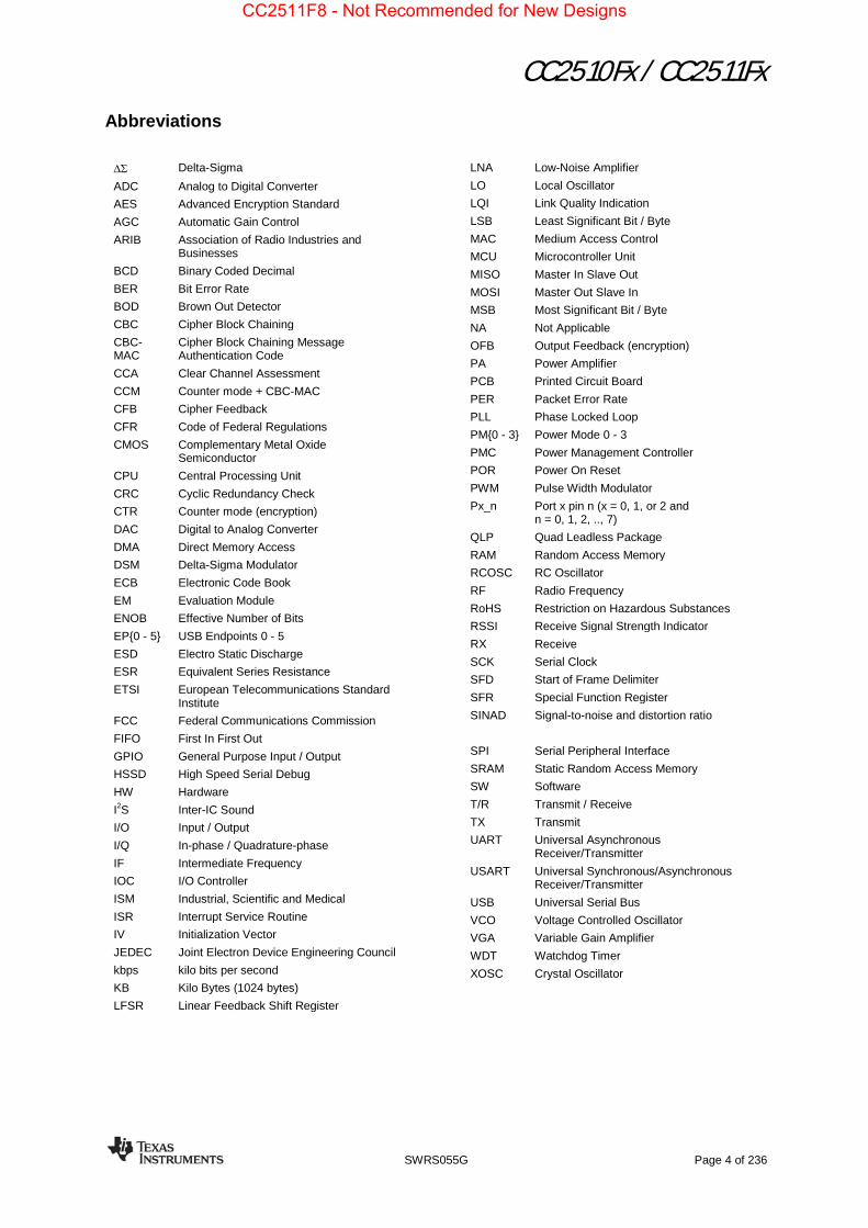


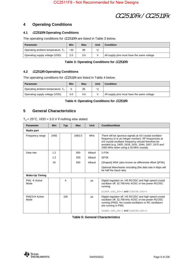

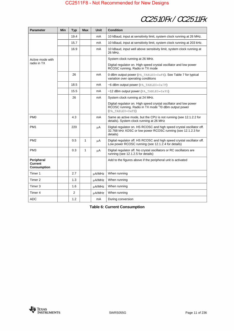

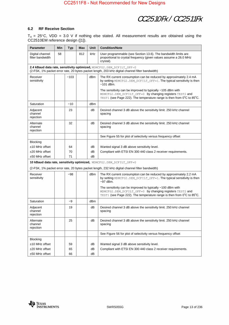


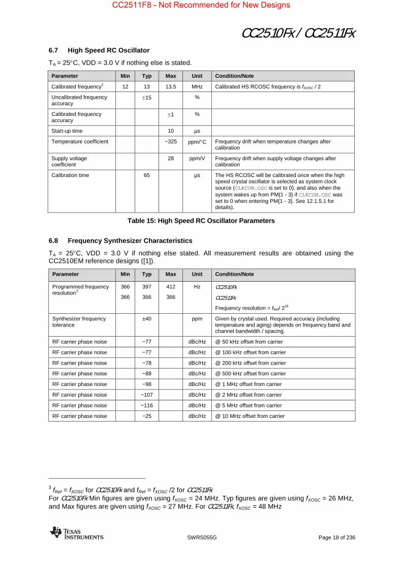
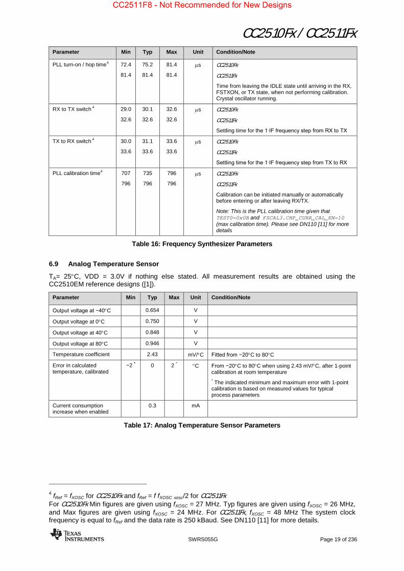

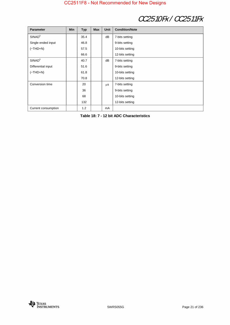

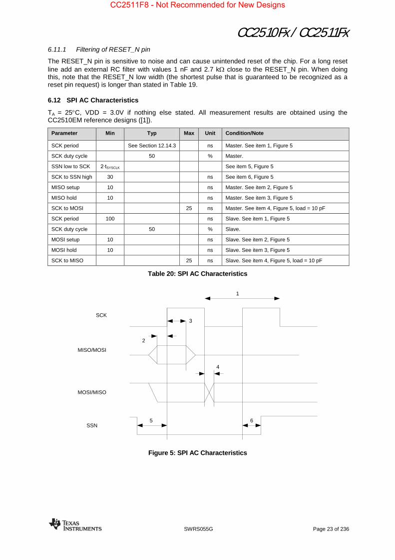

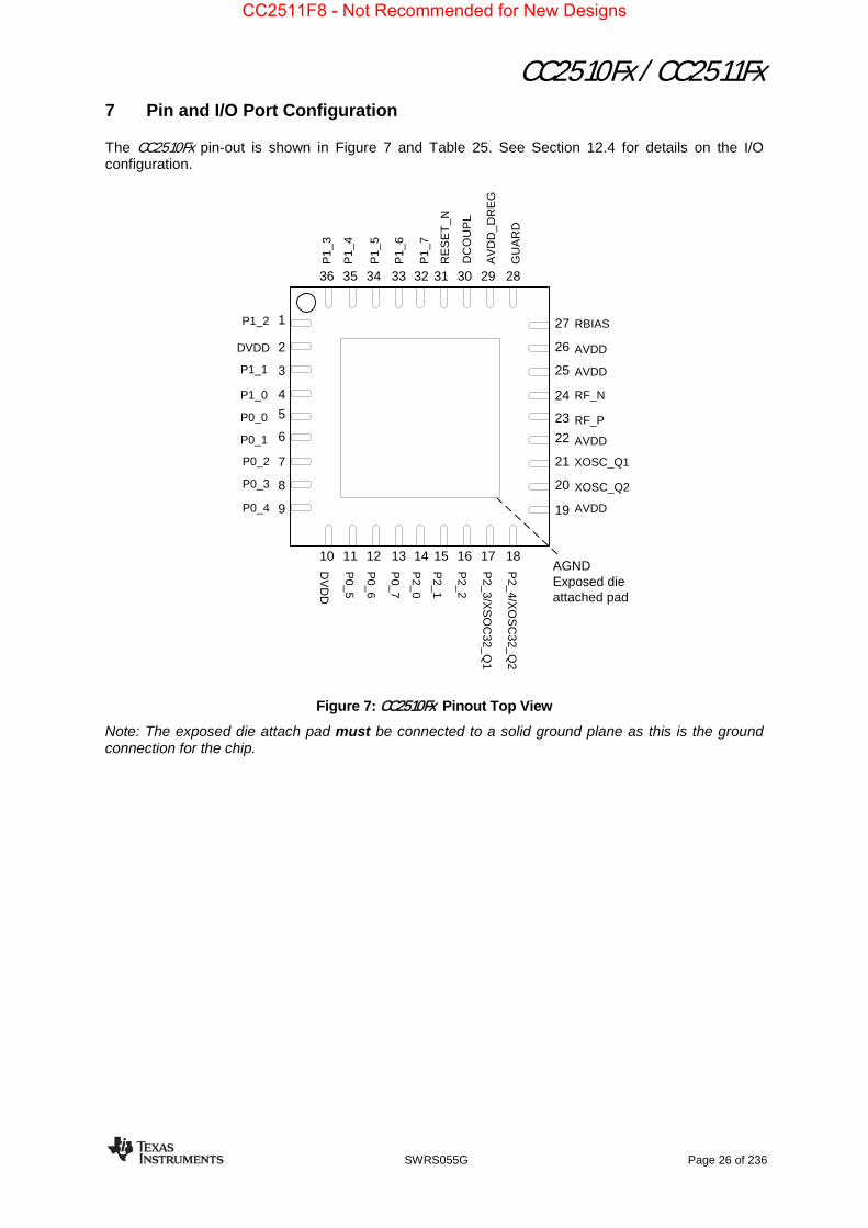

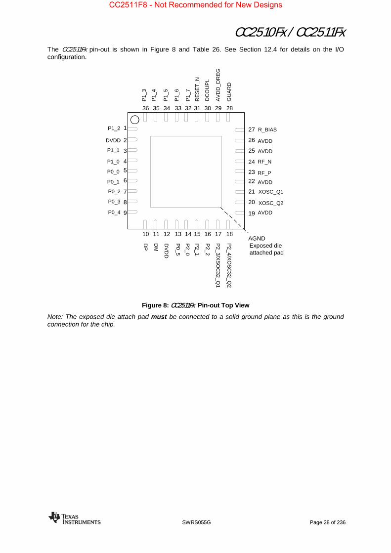

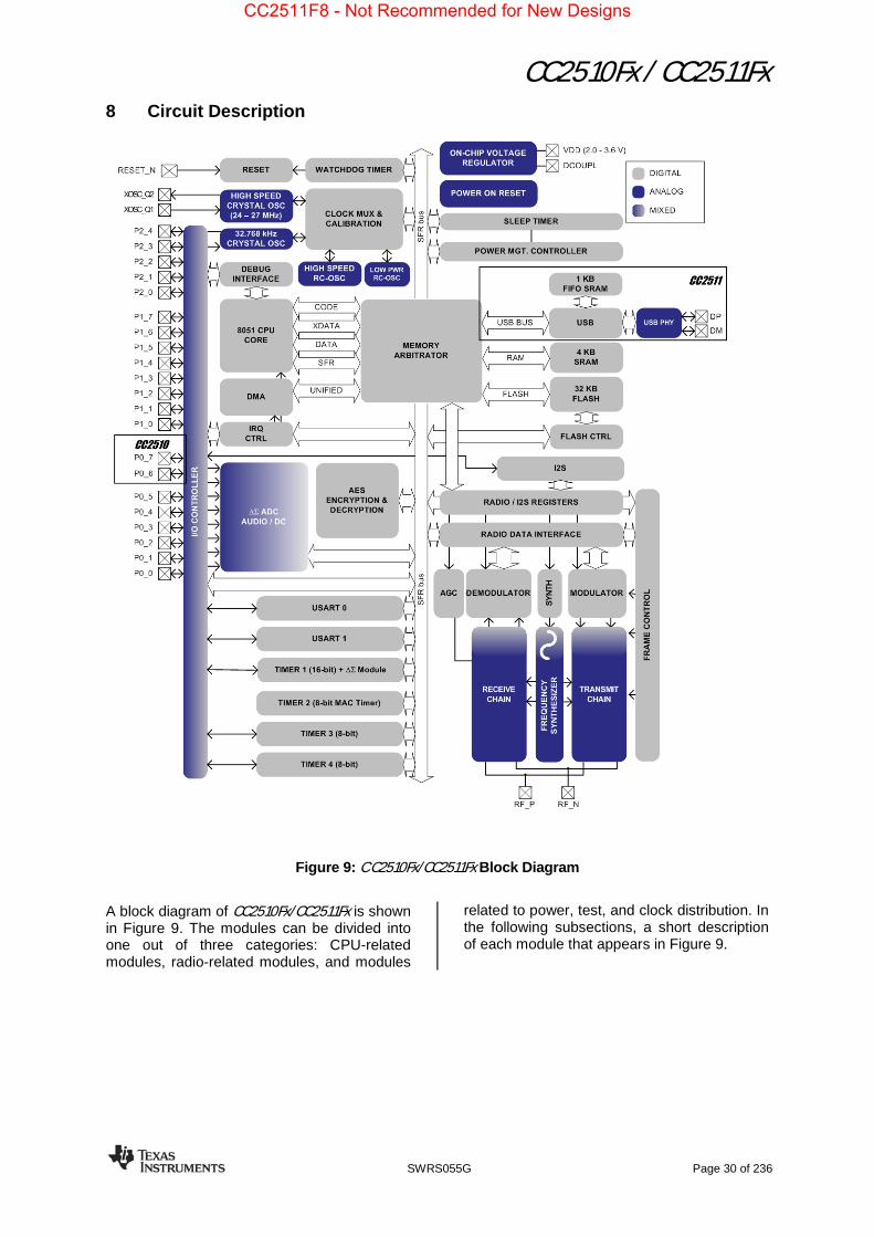


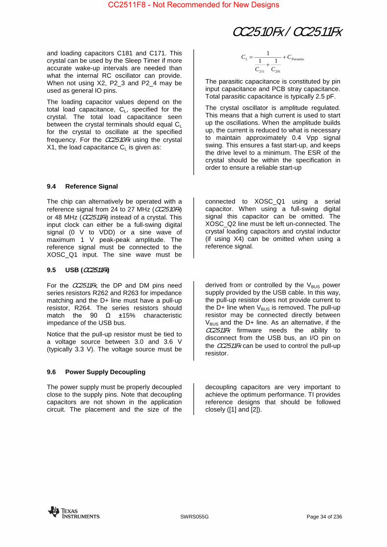


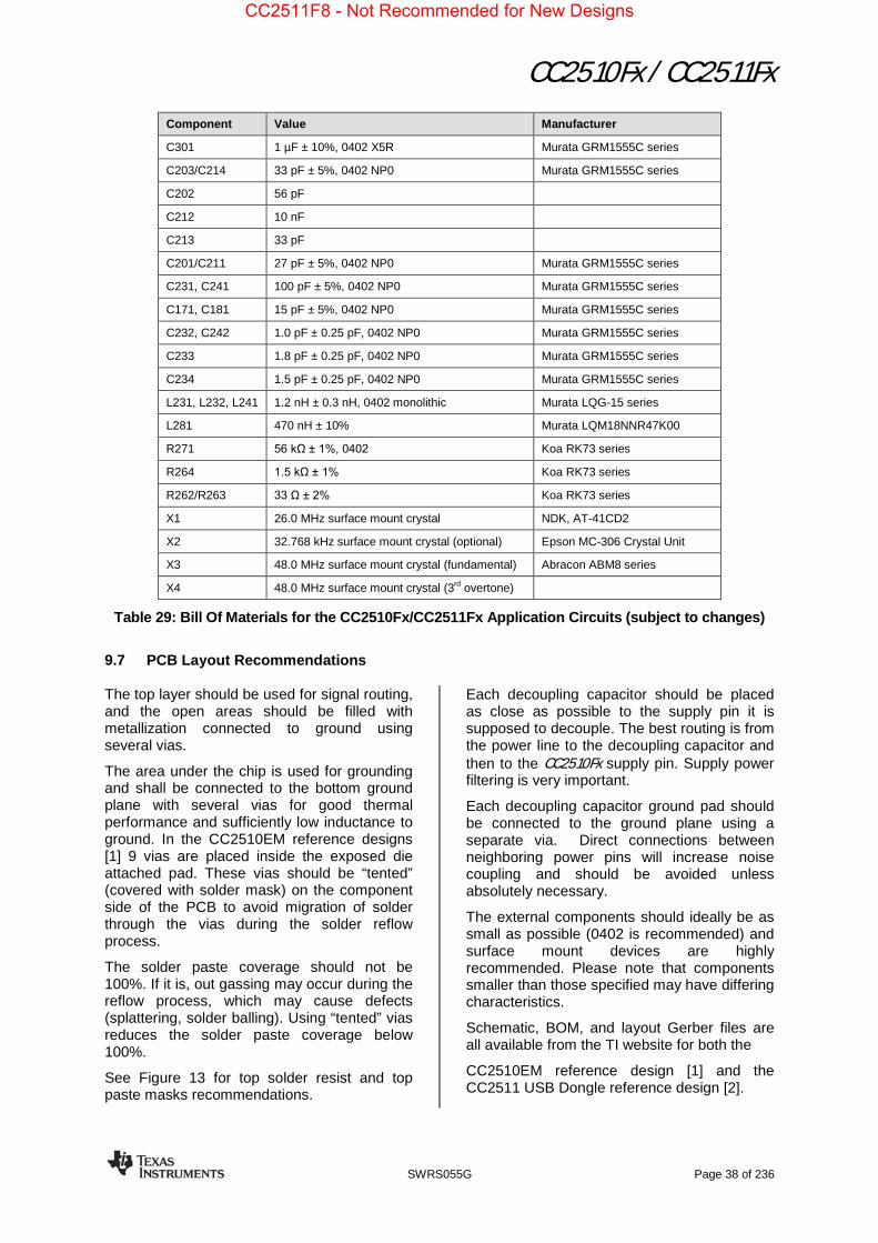

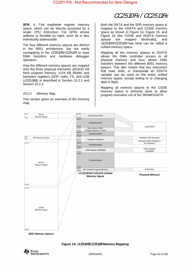


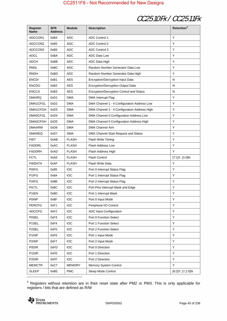
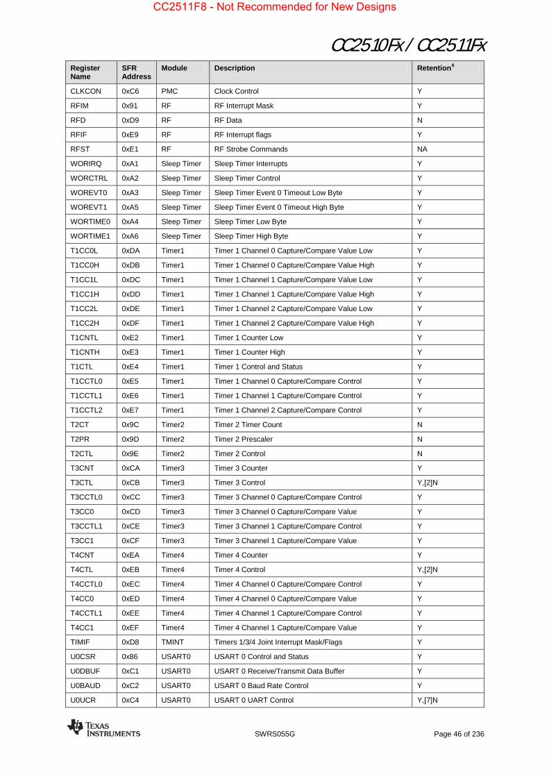

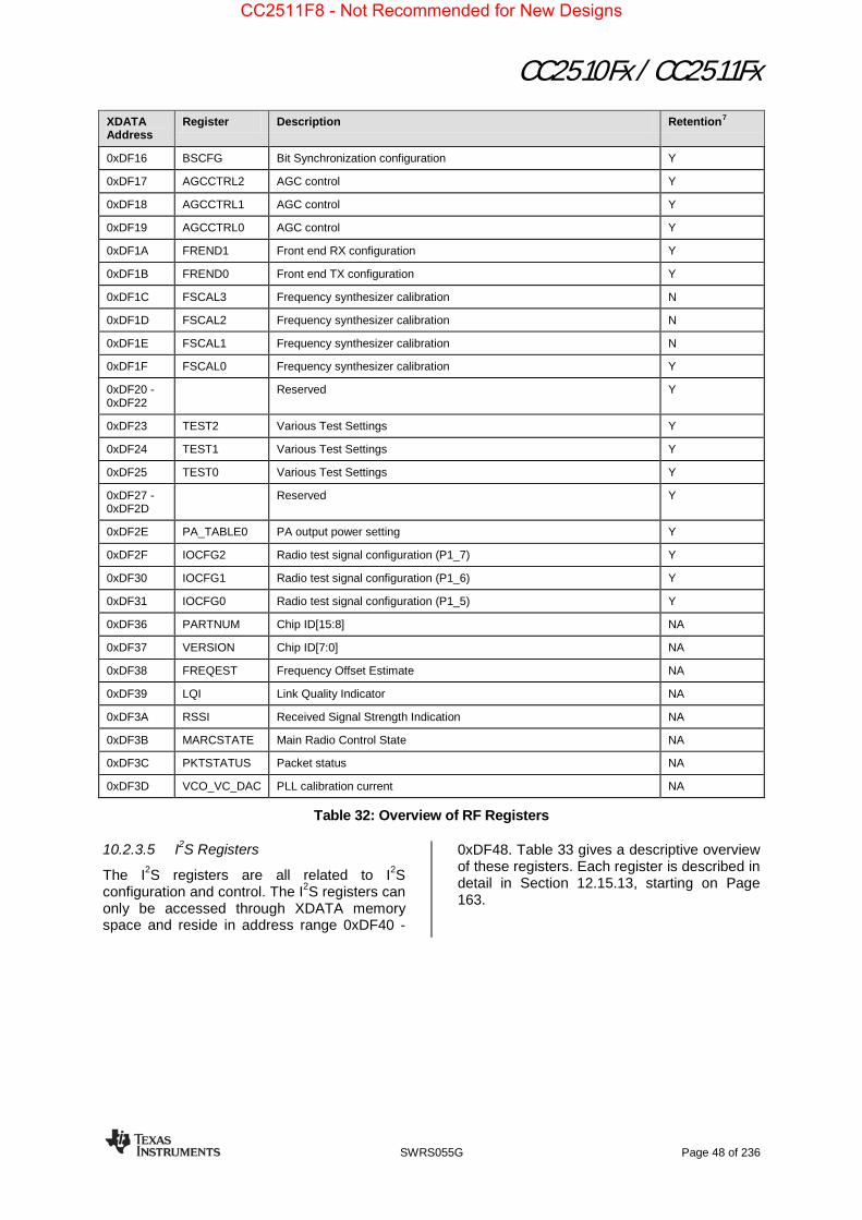

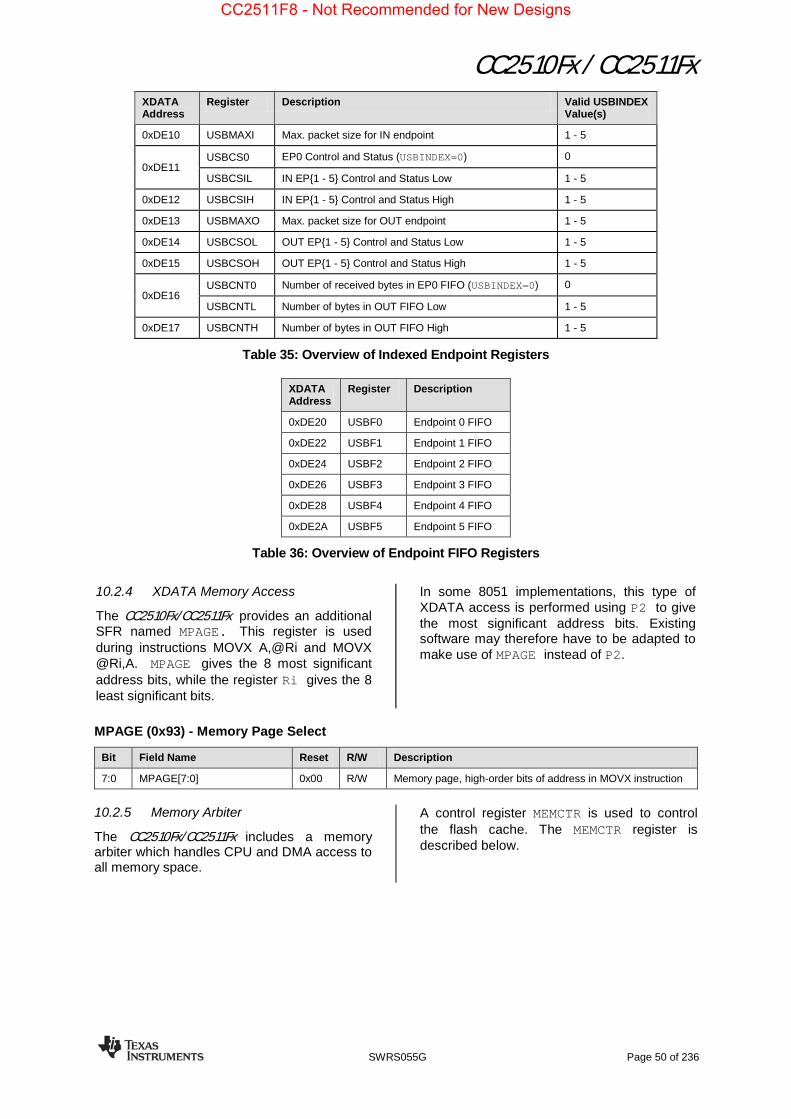

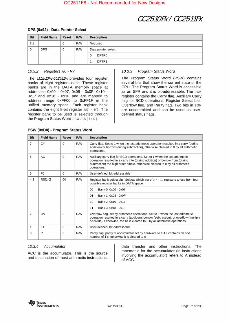


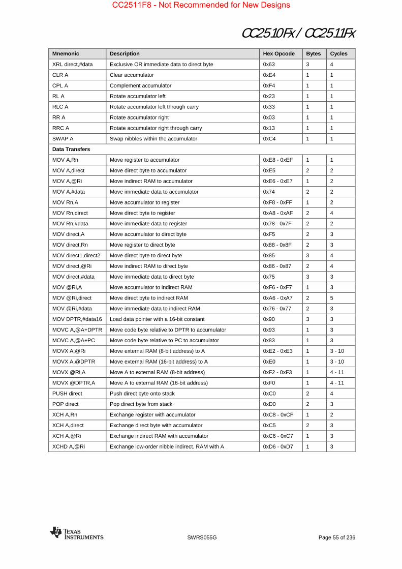


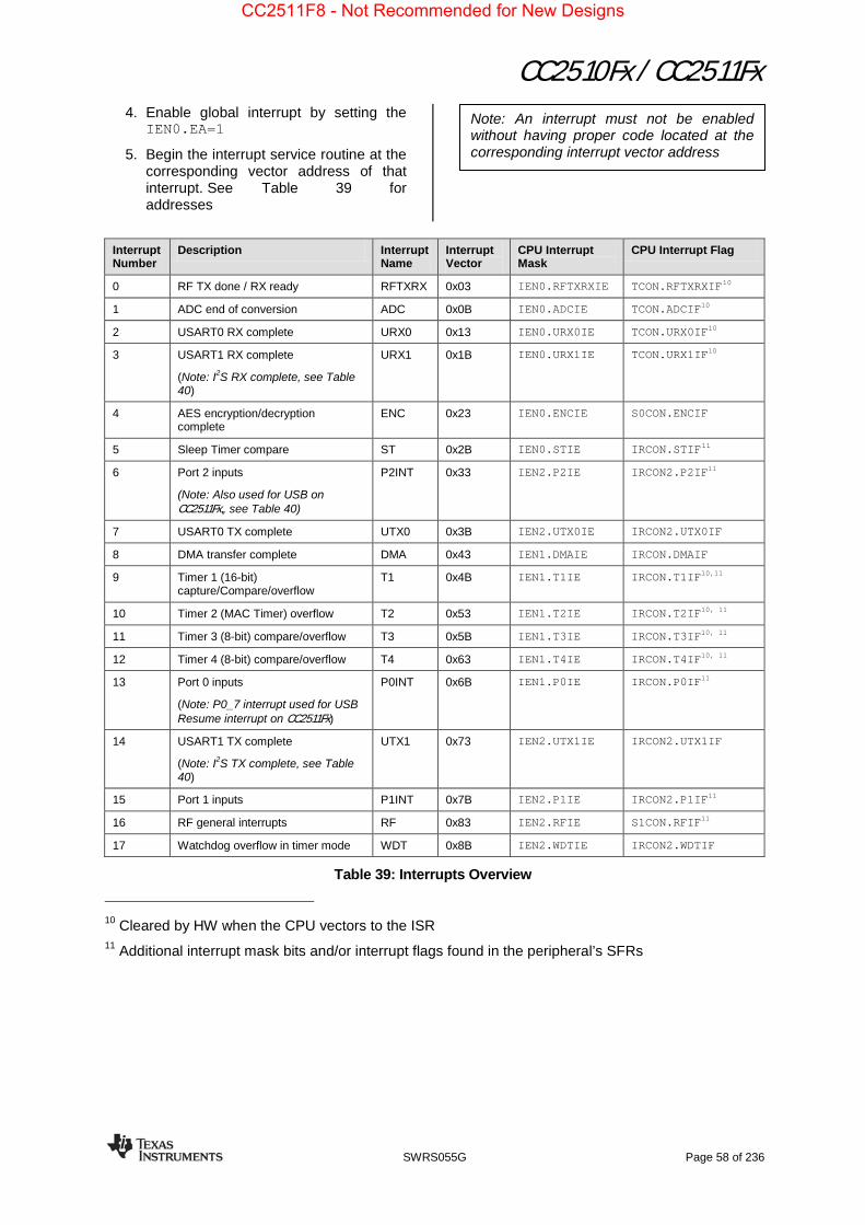

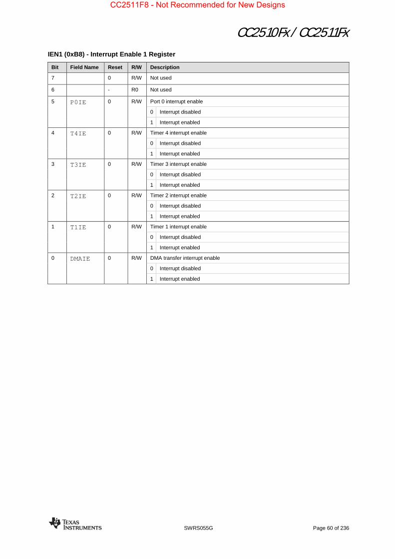
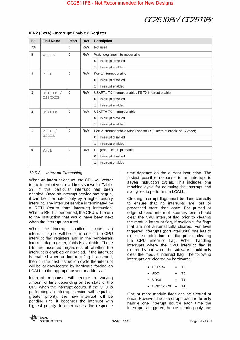


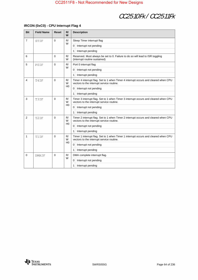


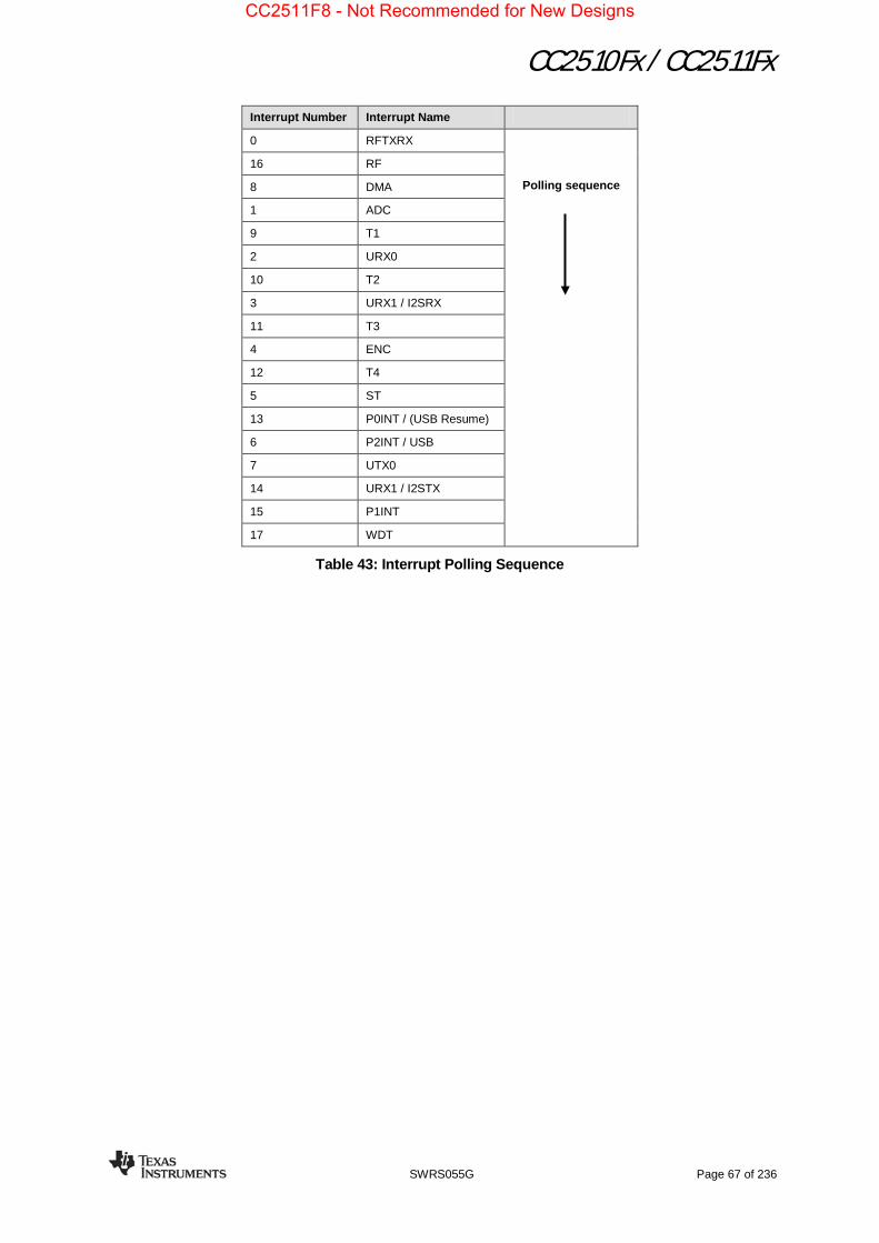


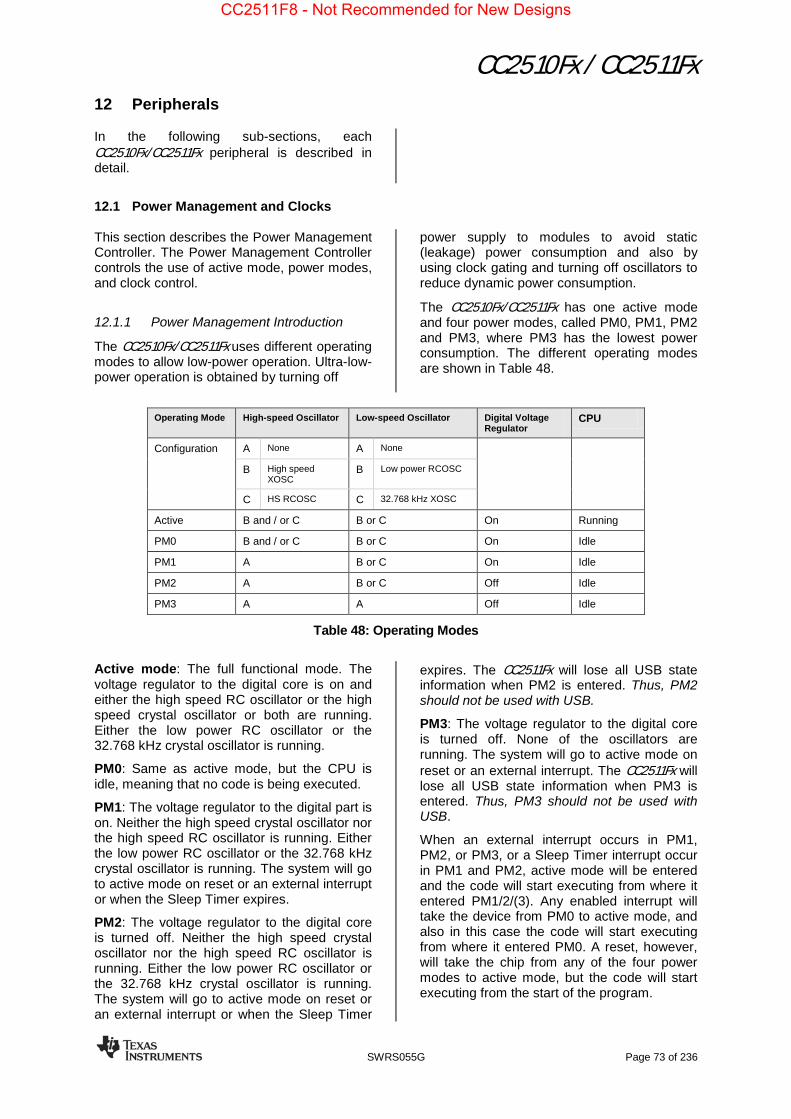


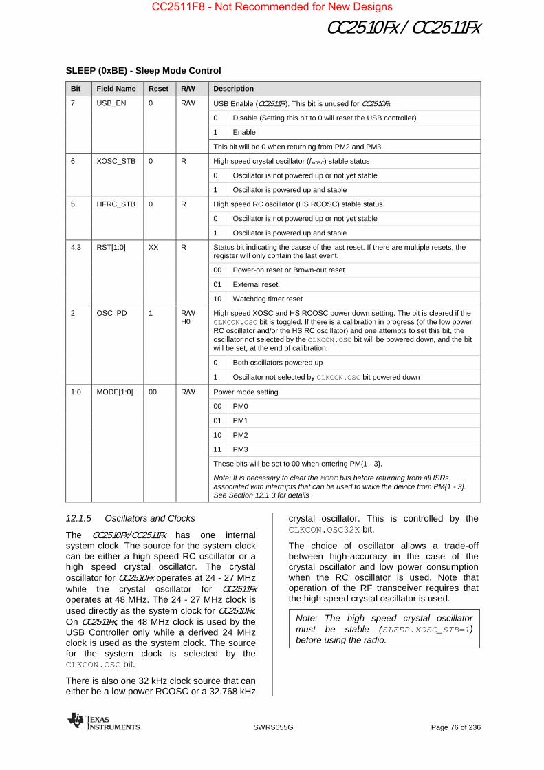


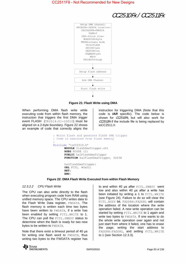
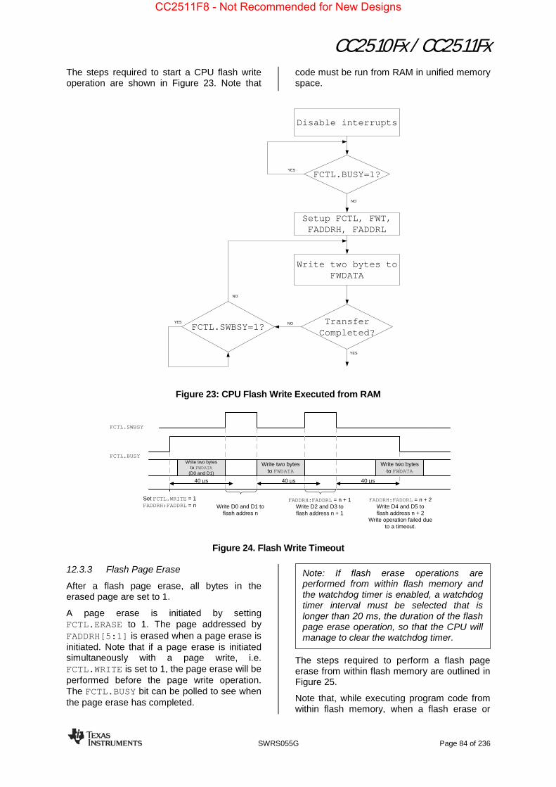


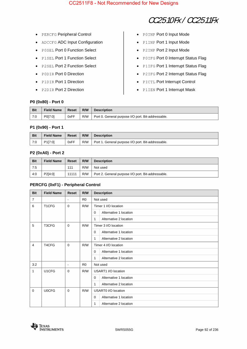


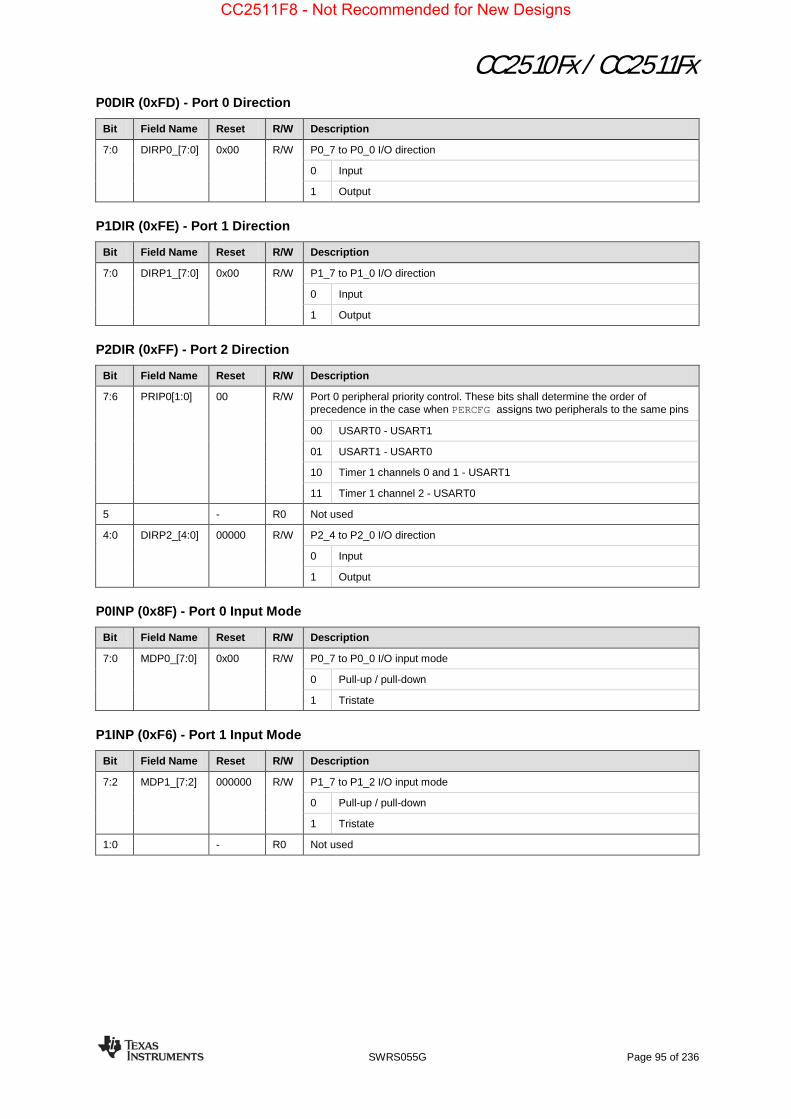
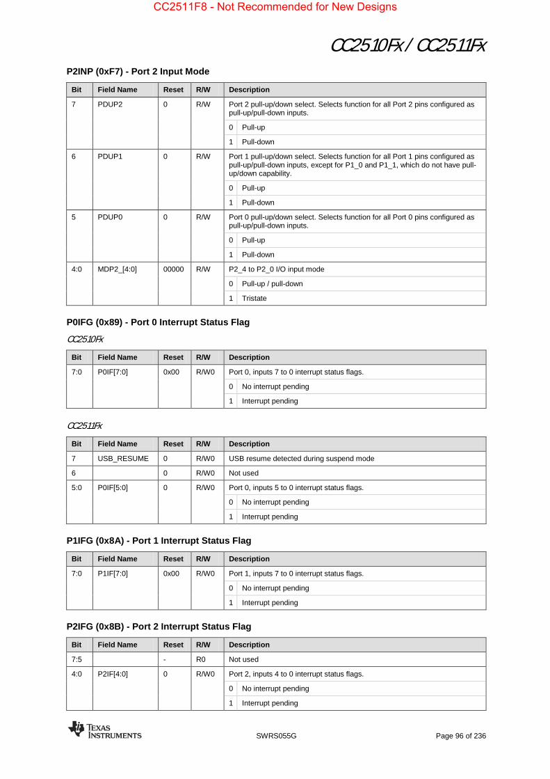


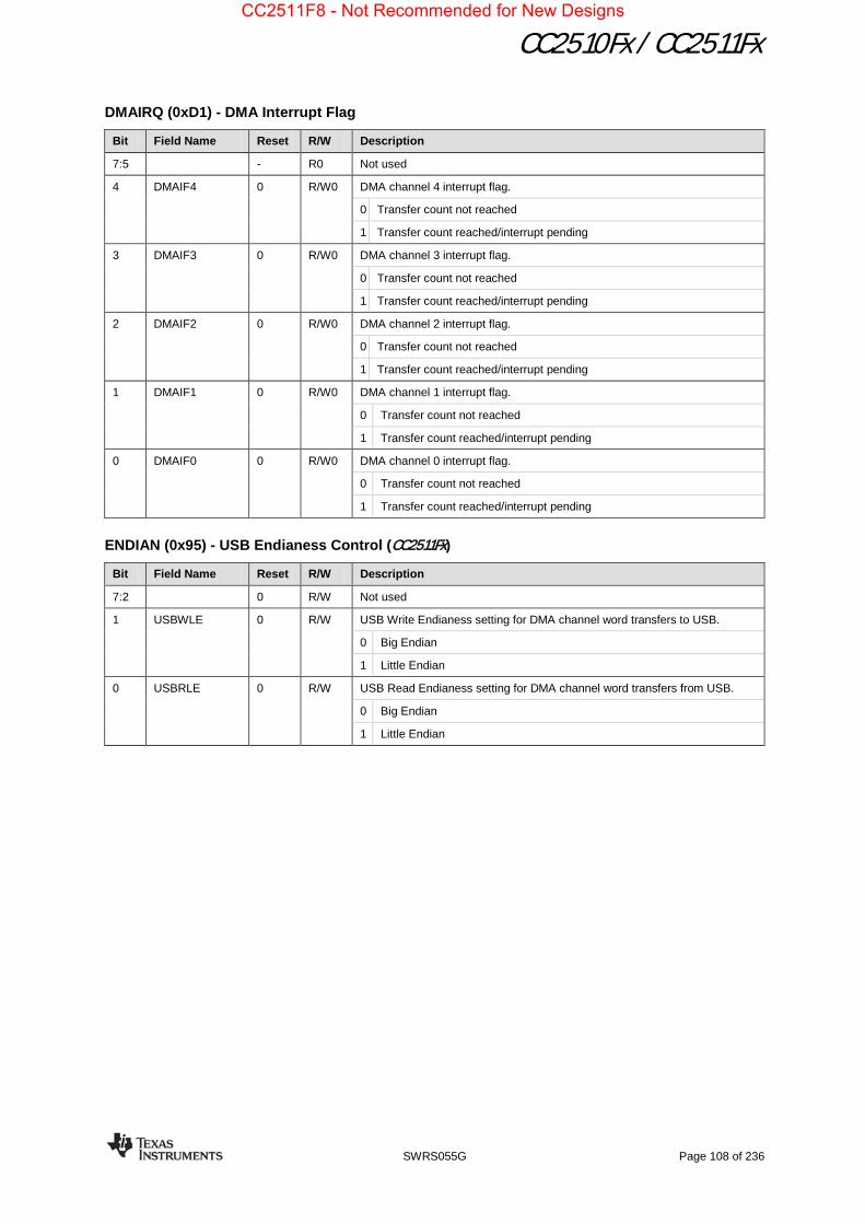
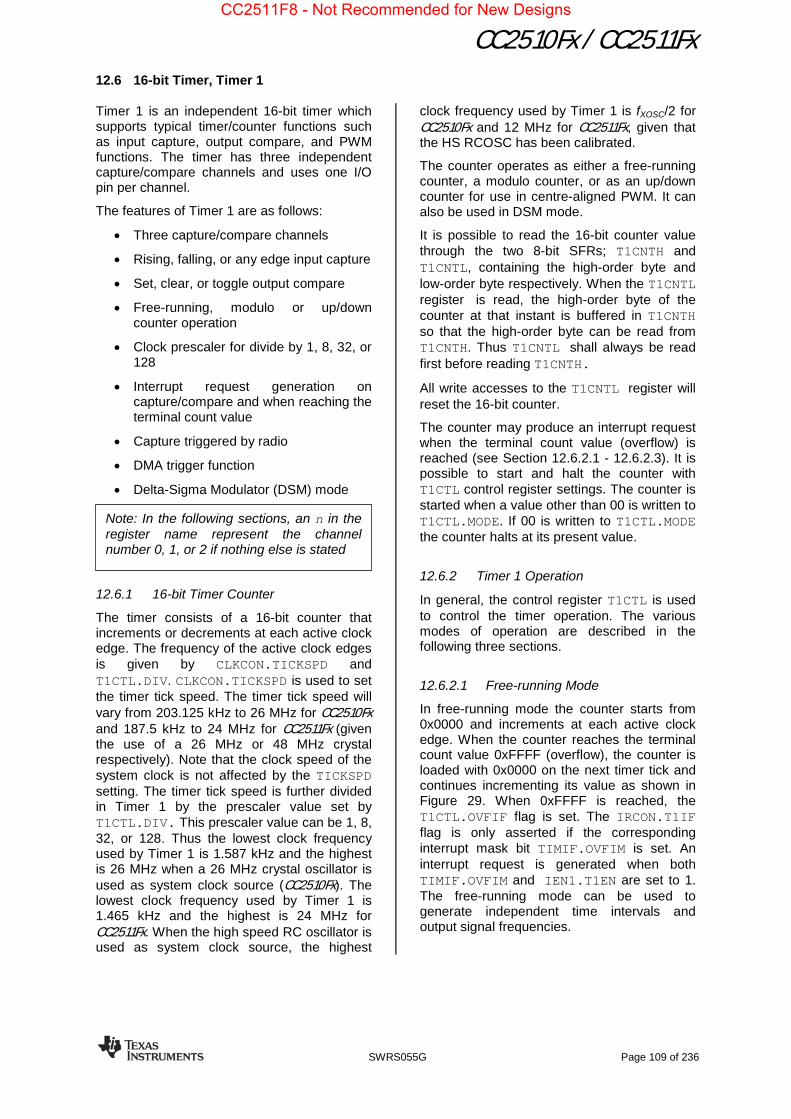
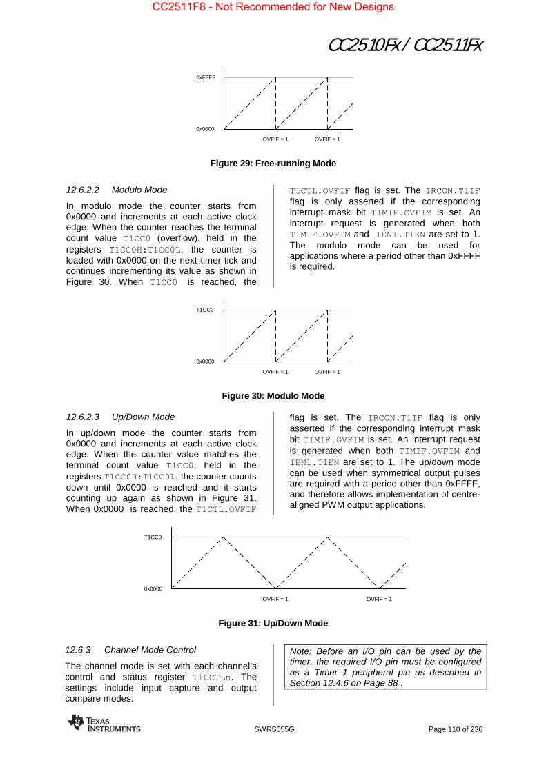
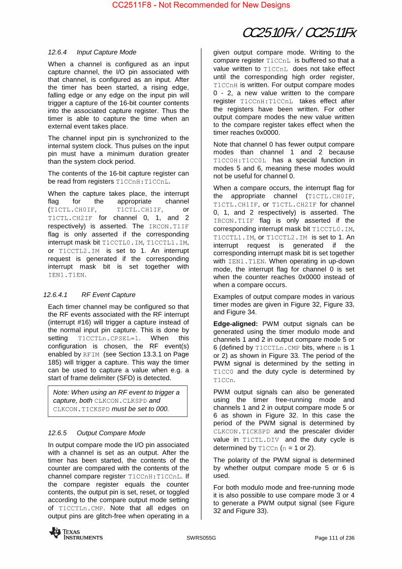
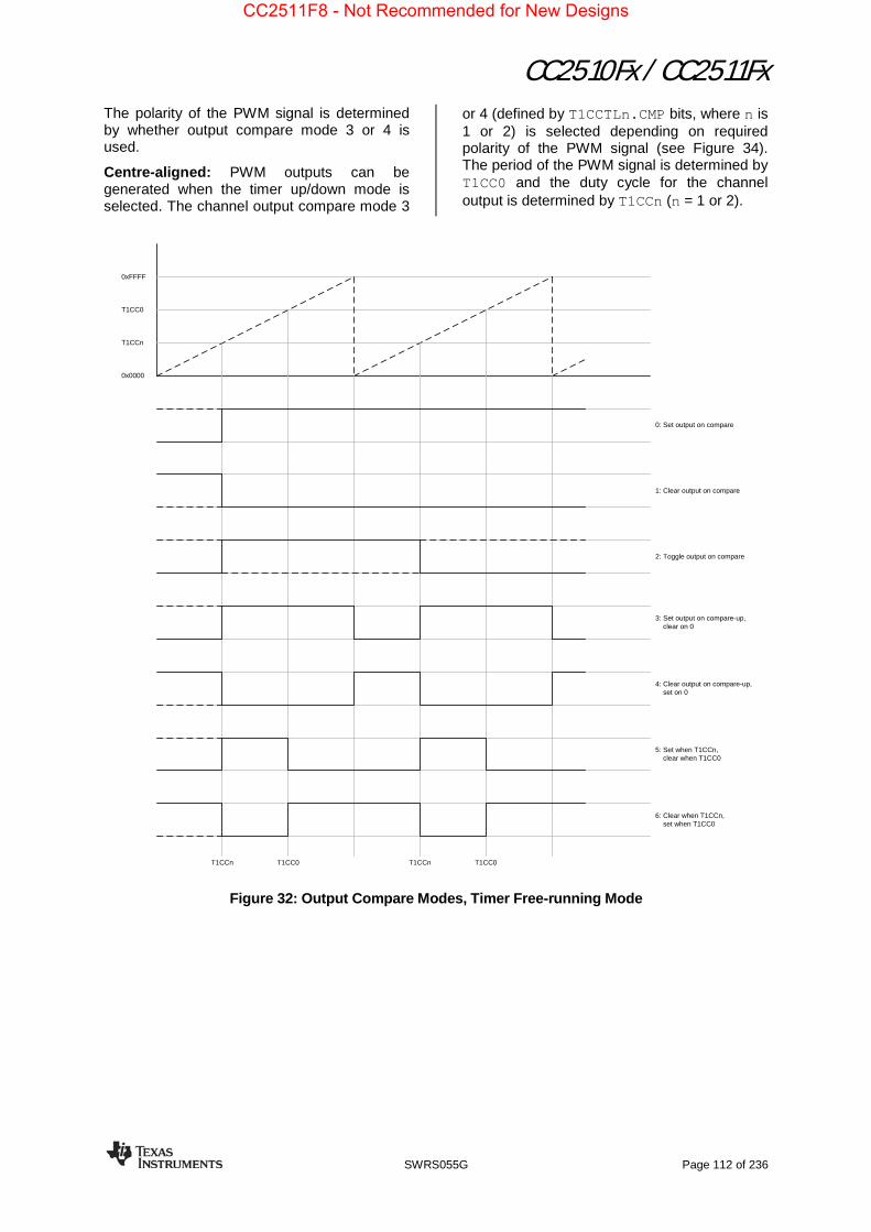

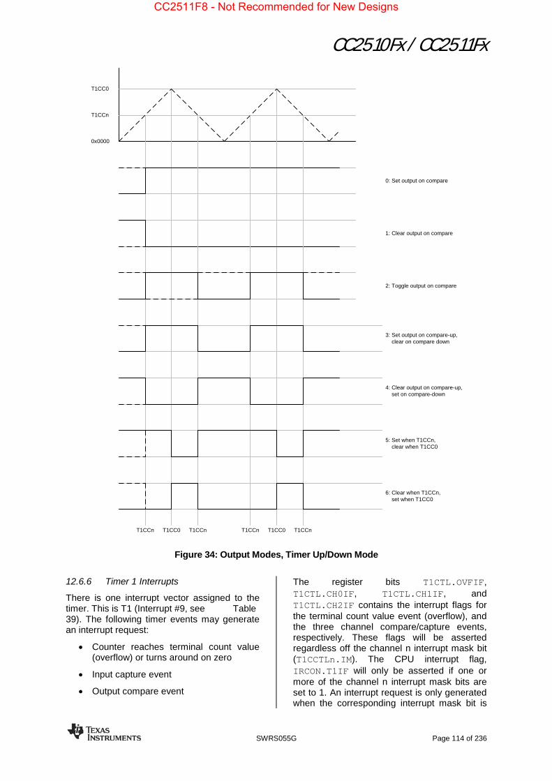


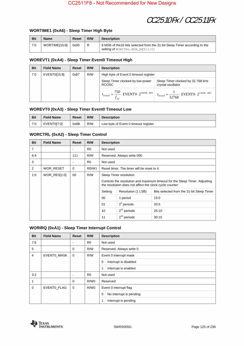

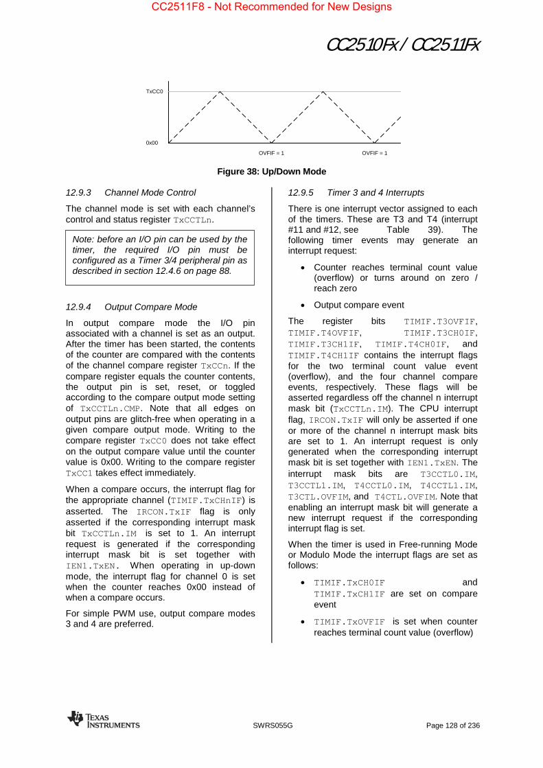


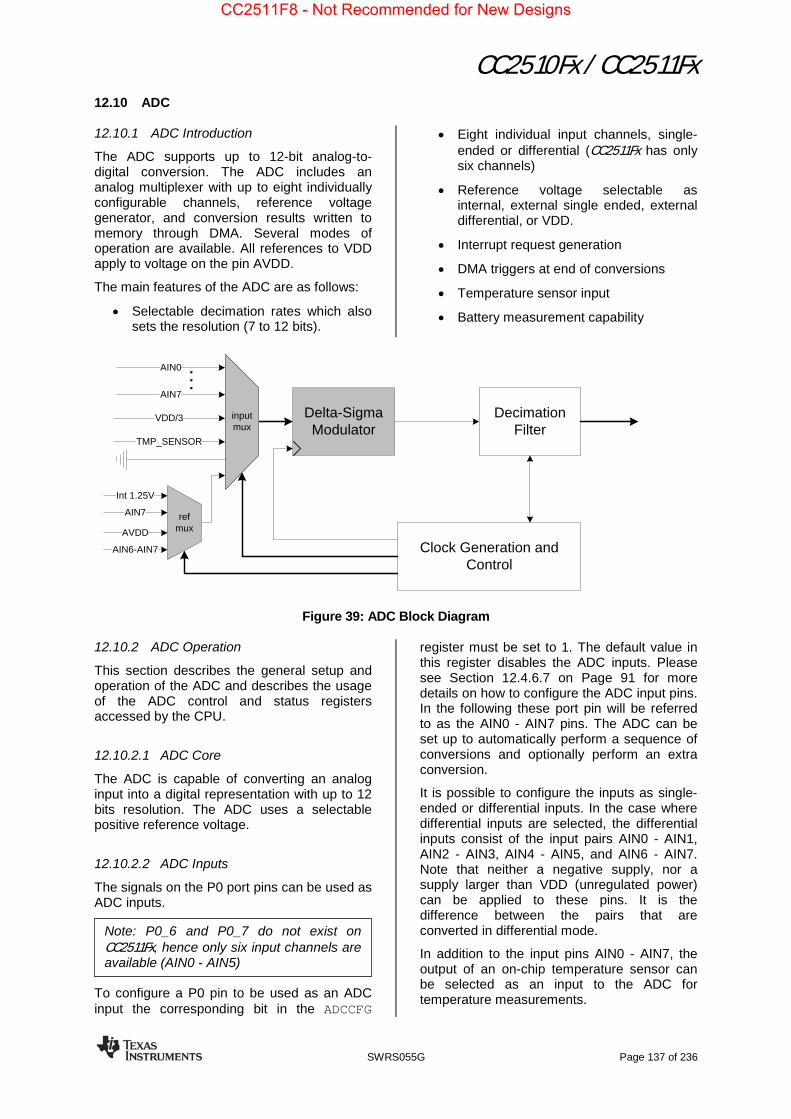


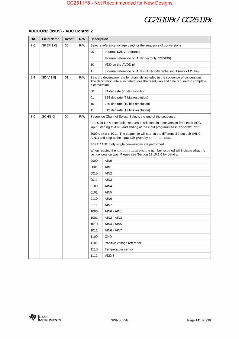


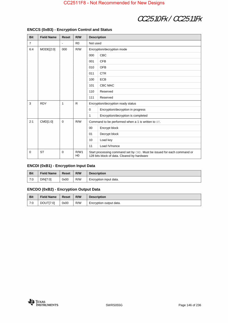


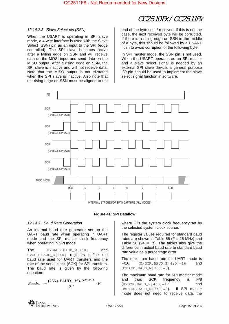

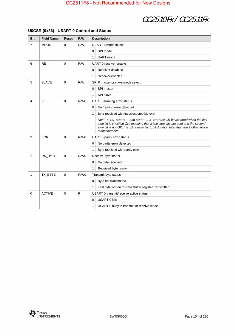
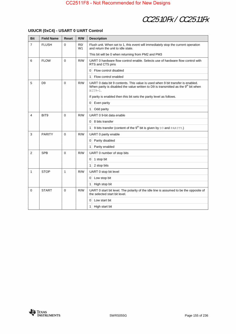

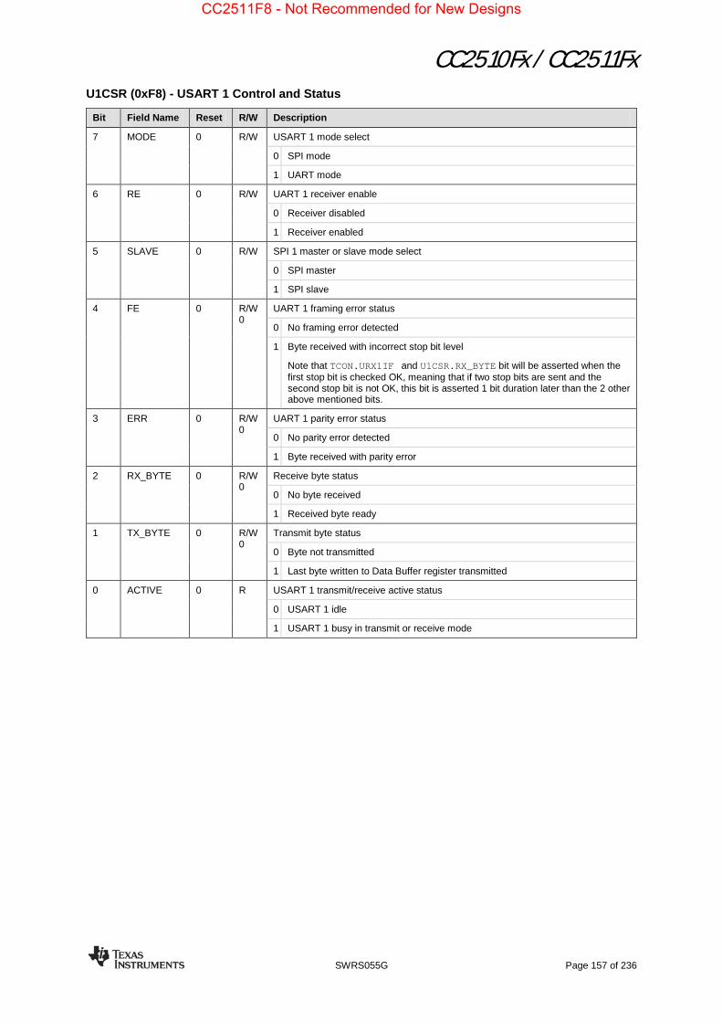


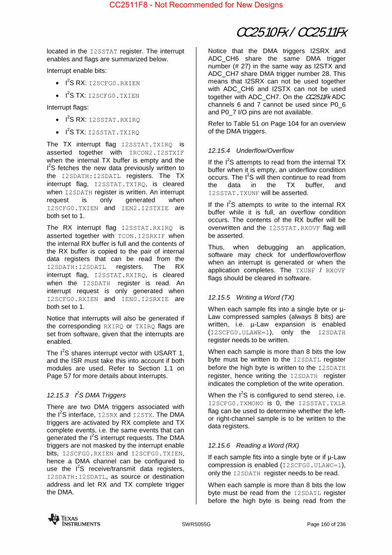


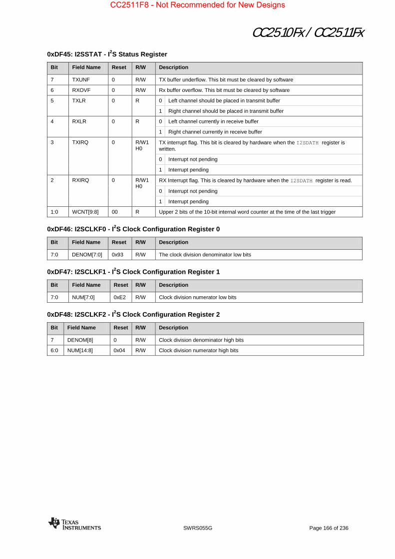


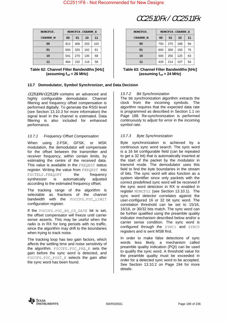


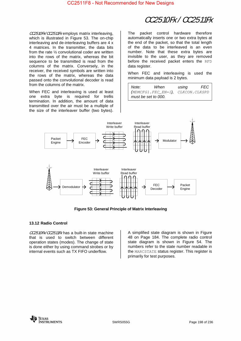
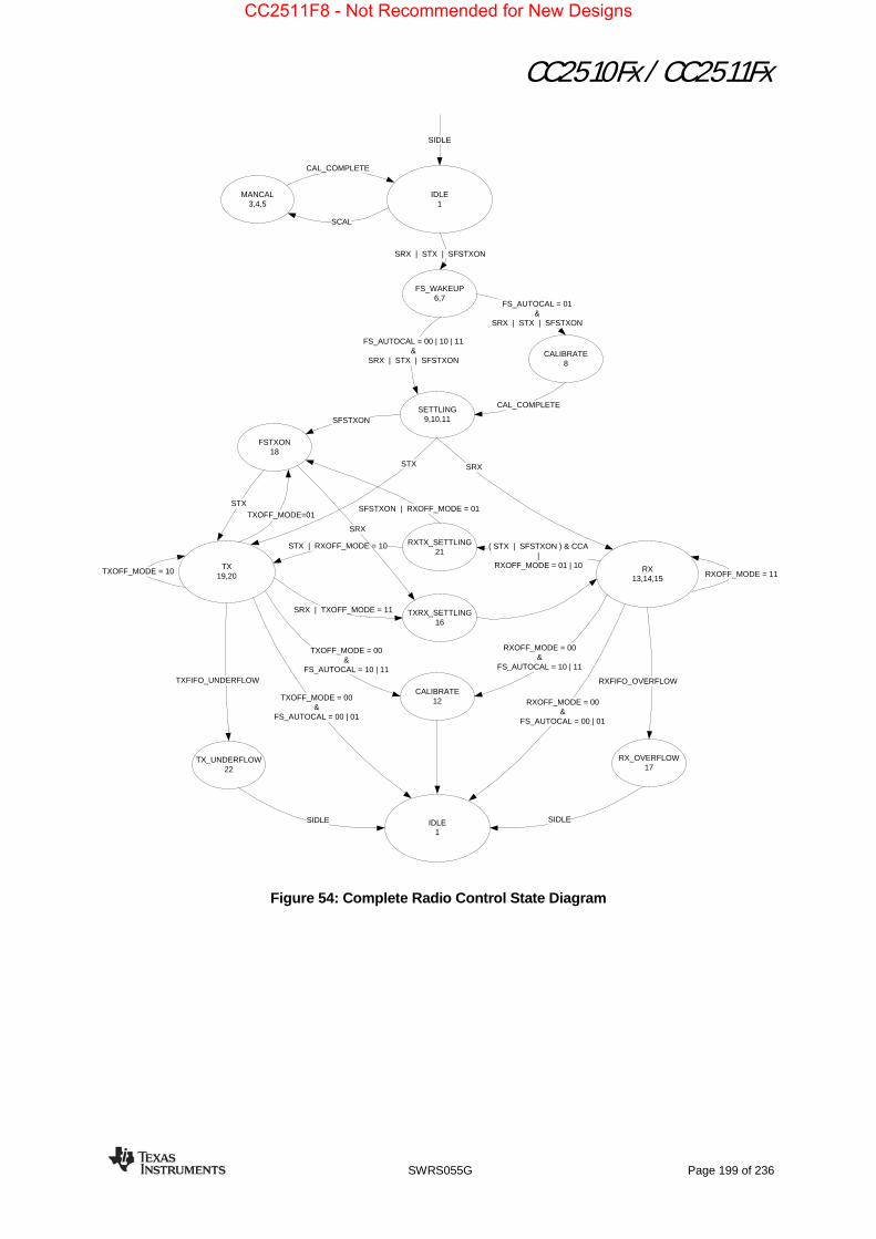


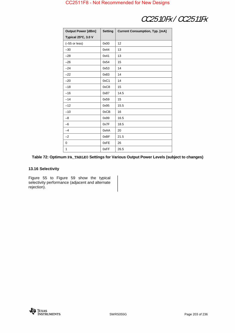

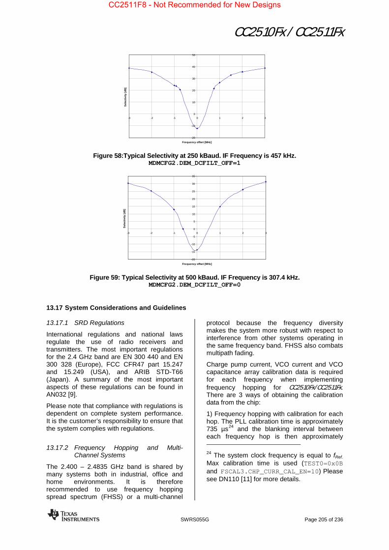


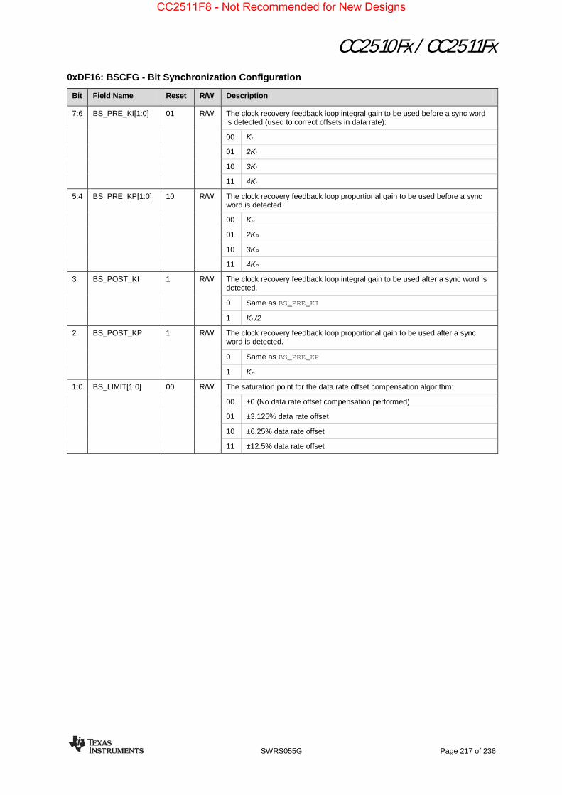

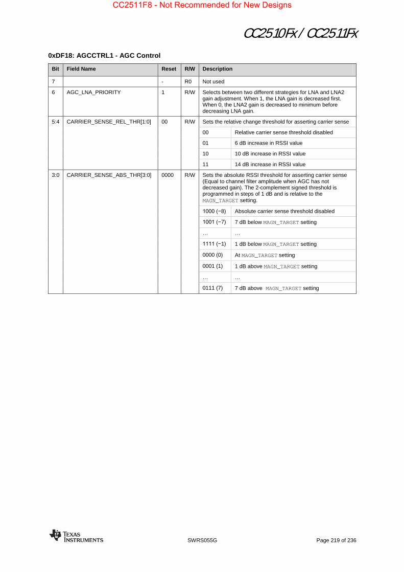
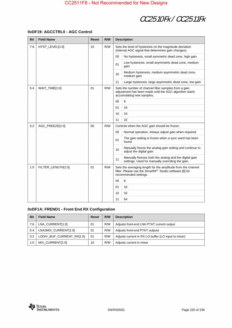
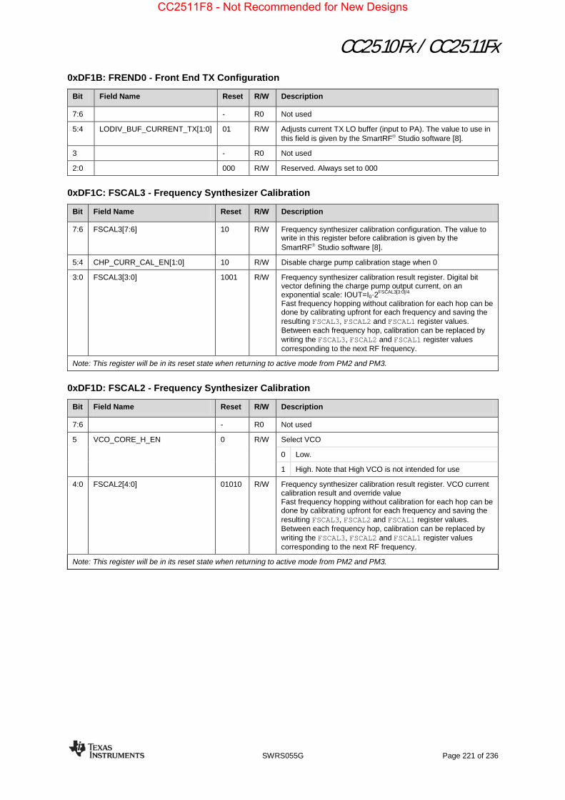

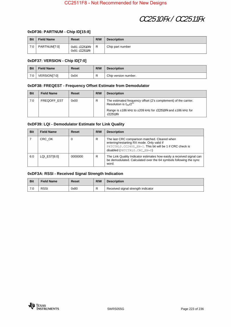


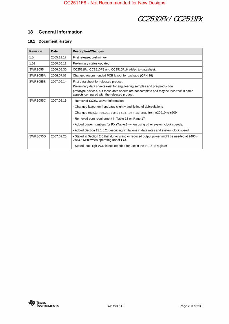
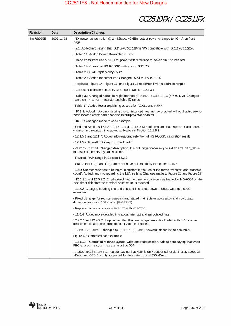


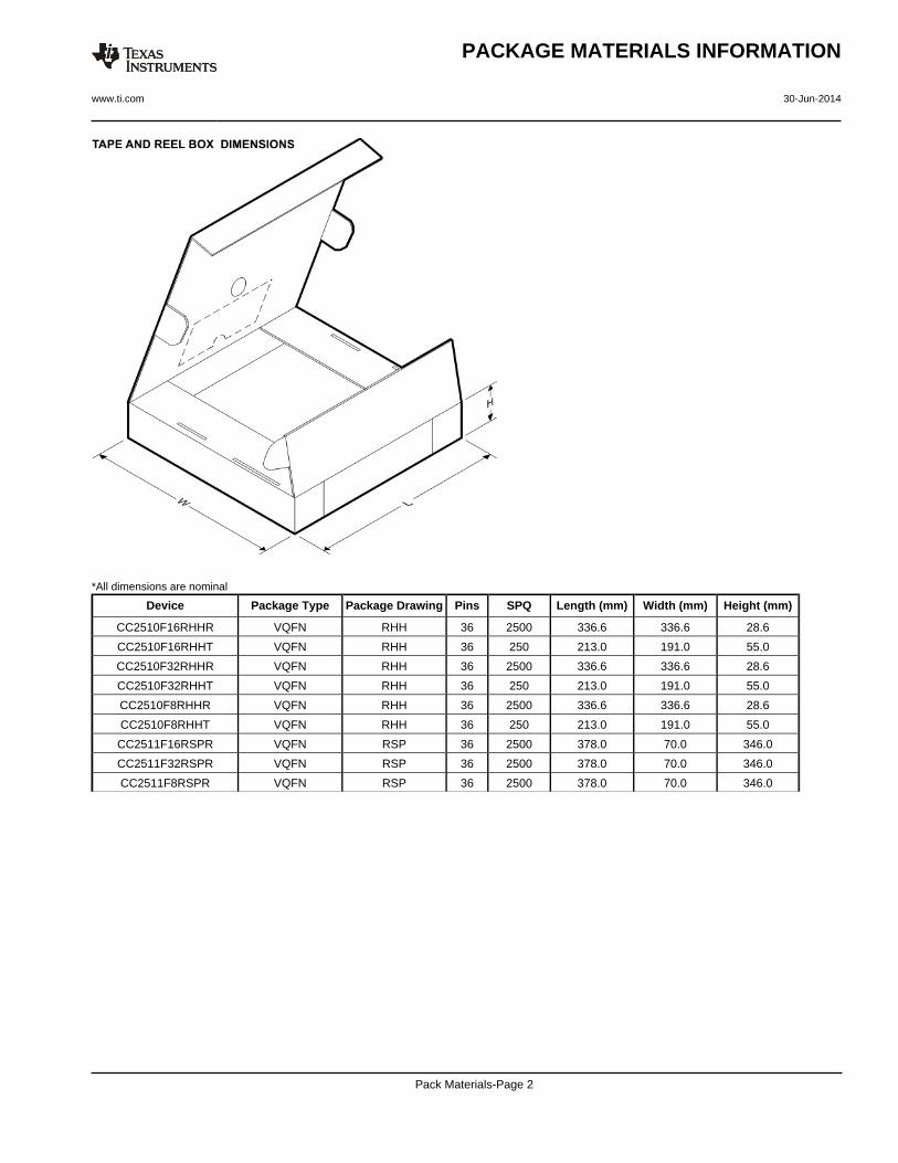

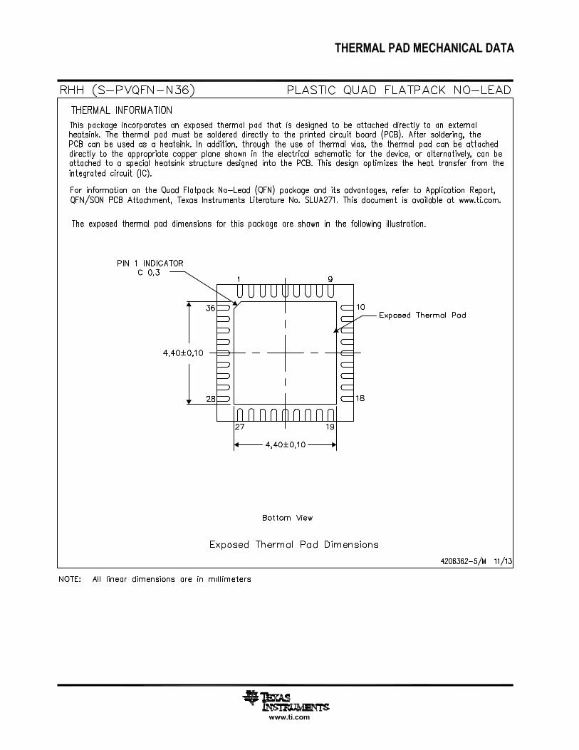
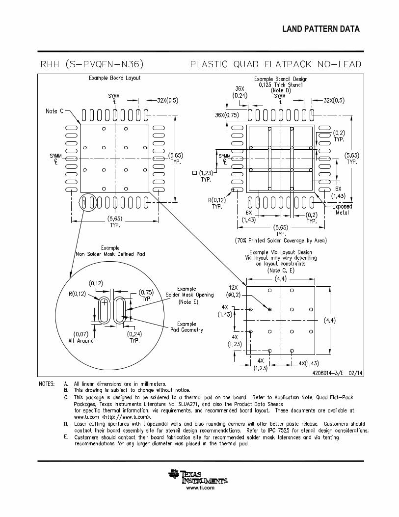
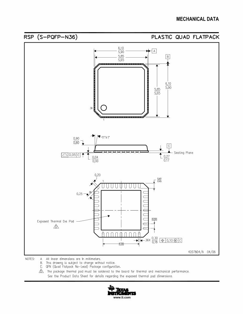


![AM1808 ARM Microprocessor datasheet (Rev. E) · Title: AM1808 ARM Microprocessor datasheet (Rev. E) Author: Texas Instruments, Incorporated [SPRS653,E ] Subject: Data Manual on Single](https://static.documents.pub/doc/80x56/60c34054293bc734be46413b/am1808-arm-microprocessor-datasheet-rev-e-title-am1808-arm-microprocessor-datasheet.jpg)


![Sealed Lead-Acid Battery Charger datasheet (Rev. C) · 2020. 12. 31. · Sealed Lead-Acid Battery Charger datasheet (Rev. C) Author: Texas Instruments, Incorporated [SLUS186,C ] Subject:](https://static.documents.pub/doc/80x56/610ffec508269627ff6a9729/sealed-lead-acid-battery-charger-datasheet-rev-c-2020-12-31-sealed-lead-acid.jpg)


![Dual Channel Power Driver datasheet (Rev. B)Title Dual Channel Power Driver datasheet (Rev. B) Author Texas Instruments, Incorporated [SLUS177,B ] Subject Data Sheet Keywords SLUS177,SLUS177B,SLUS177](https://static.documents.pub/doc/80x56/60cfbdf6eb28301c264ddccf/dual-channel-power-driver-datasheet-rev-b-title-dual-channel-power-driver-datasheet.jpg)
