Product Folder Order Now Technical Documents Tools & Software Support & Community An IMPORTANT NOTICE at the end of this data sheet addresses availability, warranty, changes, use in safety-critical applications, intellectual property matters and other important disclaimers. PRODUCTION DATA. CC3120 SWAS034 – FEBRUARY 2017 CC3120 SimpleLink™ Wi-Fi ® Wireless Network Processor, Internet-of-Things Solution for MCU Applications 1 Device Overview 1 1.1 Features 1 • CC3120R SimpleLink™ Wi-Fi ® Consists of a Wireless Network Processor (NWP) and Power- Management Subsystems • Featuring Wi-Fi Internet-on-a chip™ Dedicated ARM ® Cortex ® -M3 Microcontroller Unit (MCU) Completely Offloads Wi-Fi and Internet Protocols from the Application MCU • Wi-Fi Modes: – 802.11b/g/n Station – 802.11b/g Access Point (AP) Supports up to Four Stations – Wi-Fi Direct ® Client/Group Owner • WPA2 Personal and Enterprise Security: WEP, WPA/WPA2 PSK, WPA2 Enterprise (802.1x) • IPv4 and IPv6 TCP/IP Stack – Industry-Standard BSD Socket Application Programming Interfaces (APIs) – 16 Simultaneous TCP or UDP Sockets – 6 Simultaneous TLS and SSL Sockets • IP Addressing: Static IP, LLA, DHCPv4, and DHCPv6 With Duplicate Address Detection (DAD) • SimpleLink Connection Manager for Autonomous and Fast Wi-Fi Connections • Flexible Wi-Fi Provisioning With SmartConfig™ Technology, AP Mode, and WPS2 Options • RESTful API Support Using Internal HTTP Server • Wide Set of Security Features – Hardware Features – Separate Execution Environments – Device Identity – Networking security – Personal and Enterprise Wi-Fi Security – Secure Sockets (SSLv3, TLS1.0/1.1/TLS1.2) – HTTPS Server – Trusted Root-Certificate Catalog – TI Root-of-Trust Public key – Software IP protection – Secure Key Storage – File System Security – Software Tamper Detection – Cloning Protection • Embedded Network Applications Running on the Dedicated NWP – HTTP/HTTPS Web Server With Dynamic User Callbacks – mDNS, DNS-SD, DHCP Server – Ping • Recovery Mechanism—Can Recover to Factory Defaults or to a Complete Factory Image • Wi-Fi TX Power – 18.0 dBm @ 1 DSSS – 14.5 dBm @ 54 OFDM • Wi-Fi RX Sensitivity – –96.0 dBm @ 1 DSSS – –74.5 dBm @ 54 OFDM • Application Throughput – UDP: 16 Mbps – TCP: 13 Mbps • Power-Management Subsystem – Integrated DC-DC Converters Support a Wide Range of Supply Voltage: – VBAT Wide-Voltage Mode: 2.1 V to 3.6 V – VIO is Always Tied With VBAT – Preregulated 1.85-V Mode – Advanced Low-Power Modes – Shutdown: 1 μA – Hibernate: 4.5 μA – Low-Power Deep Sleep (LPDS): 115 μA – RX Traffic: 59 mA @ 54 OFDM – TX Traffic: 229 mA @ 54 OFDM, Maximum Power – Idle Connected (MCU in LPDS): 690 μA @ DTIM = 1 • Clock Source – 40.0-MHz Crystal With Internal Oscillator – 32.768-kHz Crystal or External RTC • RGK Package – 64-Pin, 9-mm × 9-mm Very Thin Quad Flat Nonleaded (VQFN) Package, 0.5-mm Pitch • Operating Temperature – Ambient Temperature Range: –40°C to +85°C • Device Supports SimpleLink Developers Ecosystem
Transcript
Product
Folder
Order
Now
Technical
Documents
Tools &
Software
Support &Community
An IMPORTANT NOTICE at the end of this data sheet addresses availability, warranty, changes, use in safety-critical applications,intellectual property matters and other important disclaimers. PRODUCTION DATA.
CC3120SWAS034 –FEBRUARY 2017
CC3120 SimpleLink™ Wi-Fi® Wireless Network Processor,Internet-of-Things Solution for MCU Applications
1 Device Overview
1
1.1 Features1
• CC3120R SimpleLink™ Wi-Fi® Consists of aWireless Network Processor (NWP) and Power-Management Subsystems
• Featuring Wi-Fi Internet-on-a chip™ DedicatedARM® Cortex®-M3 Microcontroller Unit (MCU)Completely Offloads Wi-Fi and Internet Protocolsfrom the Application MCU
• Wi-Fi Modes:– 802.11b/g/n Station– 802.11b/g Access Point (AP) Supports up to
Four Stations– Wi-Fi Direct® Client/Group Owner
• WPA2 Personal and Enterprise Security: WEP,WPA/WPA2 PSK, WPA2 Enterprise (802.1x)
• IPv4 and IPv6 TCP/IP Stack– Industry-Standard BSD Socket Application
Programming Interfaces (APIs)– 16 Simultaneous TCP or UDP Sockets– 6 Simultaneous TLS and SSL Sockets
• IP Addressing: Static IP, LLA, DHCPv4, andDHCPv6 With Duplicate Address Detection (DAD)
• SimpleLink Connection Manager for Autonomousand Fast Wi-Fi Connections
• Flexible Wi-Fi Provisioning With SmartConfig™Technology, AP Mode, and WPS2 Options
• RESTful API Support Using Internal HTTP Server• Wide Set of Security Features
– Hardware Features– Separate Execution Environments– Device Identity
– Networking security– Personal and Enterprise Wi-Fi Security– Secure Sockets (SSLv3, TLS1.0/1.1/TLS1.2)– HTTPS Server– Trusted Root-Certificate Catalog– TI Root-of-Trust Public key
– Software IP protection– Secure Key Storage– File System Security– Software Tamper Detection– Cloning Protection
• Embedded Network Applications Running on theDedicated NWP– HTTP/HTTPS Web Server With Dynamic User
Callbacks– mDNS, DNS-SD, DHCP Server– Ping
• Recovery Mechanism—Can Recover to FactoryDefaults or to a Complete Factory Image
1.2 Applications• For Internet-of-Things (IoT) applications, such as:
– Cloud Connectivity– Internet Gateway– Home and Building Automation– Appliances– Access Control– Security Systems– Smart Energy
– Industrial Control– Smart Plug and Metering– Wireless Audio– IP Network Sensor Nodes– Asset Tracking– Medical Devices
1.3 DescriptionThe CC3120R device is part of the SimpleLink™ microcontroller (MCU) platform which consists of Wi-Fi,Bluetooth® low energy, Sub-1 GHz and host MCUs, which all share a common, easy-to-use developmentenvironment with a single core software development kit (SDK) and rich tool set. A one-time integration ofthe SimpleLink platform enables you to add any combination of the portfolio’s devices into your design,allowing 100 percent code reuse when your design requirements change. For more information, visitOverview for SimpleLink™ solutions.
Connect any microcontroller (MCU) to the Internet of Things (IoT) cloud with the CC3120R device fromTexas Instruments™. The Wi-Fi® Alliance CERTIFIED® CC3120R device is part of the second generationof the SimpleLink™ Wi-Fi family that dramatically simplifies the implementation of low-power Internetconnectivity.
The CC3120R has all of the Wi-Fi and Internet protocols implemented in the ROM, which runs from thededicated on-chip ARM® network processor and significantly offloads the host MCU and simplifies thesystem integration.
The CC3120R Wi-Fi Internet-on-a chip™ device contains a dedicated ARM MCU that offloads many of thenetworking activities from the host MCU. This subsystem includes an 802.11b/g/n radio, baseband, andMAC with a powerful crypto engine for fast, secure Internet connections with 256-bit encryption. TheCC3120R device supports station, AP, and Wi-Fi direct modes. The device also supports WPA2 personaland enterprise security. The device includes embedded TCP/IP and TLS/SSL stacks, an HTTP server,and multiple Internet protocols. The CC3120R device supports a variety of Wi-Fi provisioning methods,including HTTP based on AP mode, SmartConfig™ technology, and WPS2.0.
As part of TI’s SimpleLink Wi-Fi family second generation, the CC3120R device introduces the newfeatures and enhanced capabilities, such as the following:
IPv6Enhanced Wi-Fi provisioningEnhanced power consumptionWi-Fi AP connection with up to four stationsMore concurrently opened BSD sockets; up to 16 BSD sockets, of which 6 are secureHTTPS supportRESTful API supportAsymmetric keys crypto library
The CC3120R device is delivered with a slim and user-friendly host driver to simplify the integration anddevelopment of networking applications. The host driver can easily be ported to most platforms andoperating systems (OS). The driver is written in strict ANSI-C (C89) and requires minimal platformadaptation layer (porting layer). The driver has a small memory footprint and can run on 8-, 16-, or 32-bitmicrocontrollers with any clock speed (no performance or real-time dependency).
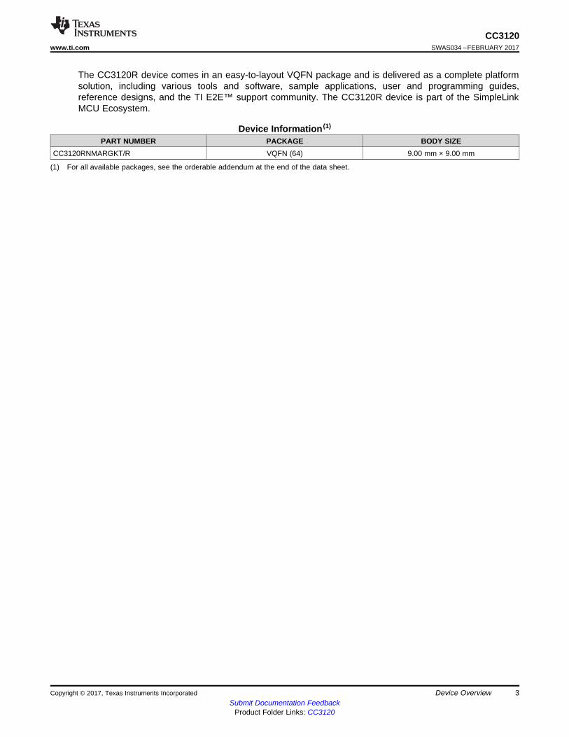
The CC3120R device comes in an easy-to-layout VQFN package and is delivered as a complete platformsolution, including various tools and software, sample applications, user and programming guides,reference designs, and the TI E2E™ support community. The CC3120R device is part of the SimpleLinkMCU Ecosystem.
(1) For all available packages, see the orderable addendum at the end of the data sheet.
Device Information (1)
PART NUMBER PACKAGE BODY SIZECC3120RNMARGKT/R VQFN (64) 9.00 mm × 9.00 mm
(1) I = InputO = Output RF = radio frequencyI/O = bidirectional
3.2 Pin AttributesTable 3-1 describes the CC3120R pins.
NOTEIf an external device drives a positive voltage to signal pads when the CC3120R device isnot powered, DC current is drawn from the other device. If the drive strength of the externaldevice is adequate, an unintentional wakeup and boot of the CC3120R device can occur. Toprevent current draw, TI recommends one of the following:• All devices interfaced to the CC3120R device must be powered from the same power rail
as the CC3120R device.• Use level shifters between the CC3120R device and any external devices fed from other
independent rails.• The nRESET pin of the CC3120R device must be held low until the VBAT supply to the
device is driven and stable.
Table 3-1. Pin Attributes
PIN DEFAULT FUNCTION STATE AT RESETAND HIBERNATE I/O TYPE (1) DESCRIPTION
2 nHIB Hi-Z I
Hibernate signal input to the NWP subsystem(active low). This is connected to the MCUGPIO. If the GPIO from the MCU can floatwhile the MCU enters low power, consideradding a pullup resistor on the board to avoidfloating.
3 Reserved Hi-Z – Reserved for future use5 HOST_SPI_CLK Hi-Z I Host interface SPI clock6 HOST_SPI_MOSI Hi-Z I Host interface SPI data input7 HOST_SPI_MISO Hi-Z O Host interface SPI data output8 HOST_SPI_nCS Hi-Z I Host interface SPI chip select (active low)9 VDD_DIG1 Hi-Z Power Digital core supply (1.2 V)
10 VIN_IO1 Hi-Z Power I/O supply11 FLASH_SPI_CLK Hi-Z O Serial flash interface: SPI clock12 FLASH_SPI_MOSI Hi-Z O Serial flash interface: SPI data out13 FLASH _SPI_MISO Hi-Z I Serial flash interface: SPI data in (active high)
14 FLASH _SPI_CS Hi-Z O Serial flash interface: SPI chip select(active low)
15 HOST_INTR Hi-Z O Interrupt output (active high)19 Reserved Hi-Z – Connect a 100-kΩ pulldown resistor to ground.
21 SOP2/TCXO_EN Hi-Z OControls restore to default mode. Enable signalfor external TCXO. Add a 10-kΩ pulldownresistor to ground.
22 WLAN_XTAL_N Hi-Z Analog Connect the WLAN 40-MHz XTAL here.23 WLAN_XTAL_P Hi-Z Analog Connect the WLAN 40-MHz XTAL here.24 VDD_PLL Hi-Z Power Internal PLL power supply (1.4 V nominal)25 LDO_IN2 Hi-Z Power Input to internal LDO29
Reserved Hi-Z O Reserved for future use3031 RF_BG Hi-Z RF 2.4-GHz RF TX, RX
32 nRESET Hi-Z IRESET input for the device. Active low input.Use RC circuit (100 k || 0.1 µF) for power onreset (POR).
PIN DEFAULT FUNCTION STATE AT RESETAND HIBERNATE I/O TYPE (1) DESCRIPTION
33 VDD_PA_IN Hi-Z Power Power supply for the RF power amplifier (PA)
34 SOP1 Hi-Z – Controls restore to default mode. Add 100-kΩpulldown to ground. Factory default function.
35 SOP0 Hi-Z – Controls restore to default mode. Add 100-kΩpulldown to ground. Factory default function.
36 LDO_IN1 Hi-Z Power Input to internal LDO
37 VIN_DCDC_ANA Hi-Z Power Power supply for the DC-DC converter foranalog section
38 DCDC_ANA_SW Hi-Z Power Analog DC-DC converter switch output39 VIN_DCDC_PA Hi-Z Power PA DC-DC converter input supply40 DCDC_PA_SW_P Hi-Z Power PA DC-DC converter switch output +ve41 DCDC_PA_SW_N Hi-Z Power PA DC-DC converter switch output –ve
42 DCDC_PA_OUT Hi-Z Power PA DC-DC converter output. Connect theoutput capacitor for DC-DC here.
43 DCDC_DIG_SW Hi-Z Power Digital DC-DC converter switch output
44 VIN_DCDC_DIG Hi-Z Power Power supply input for the digital DC-DCconverter
45 DCDC_ANA2_SW_P Hi-Z Power Analog2 DC-DC converter switch output +ve46 DCDC_ANA2_SW_N Hi-Z Power Analog2 DC-DC converter switch output –ve47 VDD_ANA2 Hi-Z Power Analog2 power supply input48 VDD_ANA1 Hi-Z Power Analog1 power supply input49 VDD_RAM Hi-Z Power Power supply for the internal RAM50 UART1_nRTS Hi-Z O UART host interface (active low)
51 RTC_XTAL_P Hi-Z Analog 32.768-kHz XTAL_P or external CMOS levelclock input
52 RTC_XTAL_N Hi-Z Analog 32.768-kHz XTAL_N or 100-kΩ external pullupfor external clock
54 VIN_IO2 Hi-Z Power I/O power supply. Same as battery voltage.
55 UART1_TX Hi-Z O UART host interface. Connect to test point onprototype for flash programming.
56 VDD_DIG2 Hi-Z Power Digital power supply (1.2 V)
57 UART1_RX Hi-Z I UART host interface; connect to test point onprototype for flash programming.
58 TEST_58 – Test signal; connect to an external test point.59 TEST_59 – Test signal; connect to an external test point.60 TEST_60 Hi-Z O Test signal; connect to an external test point.61 UART1_nCTS Hi-Z I UART host interface (active low)62 TEST_62 Hi-Z O Test signal; connect to an external test point.
65 GND Power Ground tab used as thermal and electricalground
All measurements are referenced at the device pins, unless otherwise indicated. All specifications are overprocess and voltage, unless otherwise indicated.
4.1 Absolute Maximum Ratingsover operating free-air temperature range (unless otherwise noted)
MIN MAX UNITVBAT and VIO Pins: 37, 39, 44 –0.5 3.8 VVIO – VBAT (differential) Pins: 10, 54 0.0 VDigital inputs –0.5 VIO + 0.5 VRF pins –0.5 2.1 VAnalog pins, XTAL Pins: 22, 23, 51, 52 –0.5 2.1 VOperating temperature, TA –40 85 °CStorage temperature, Tstg –55 125 °C
(1) JEDEC document JEP155 states that 500-V HBM allows safe manufacturing with a standard ESD control process.(2) JEDEC document JEP157 states that 250-V CDM allows safe manufacturing with a standard ESD control process.
4.2 ESD RatingsVALUE UNIT
VESD Electrostatic dischargeHuman body model (HBM), per ANSI/ESDA/JEDEC JS-001 (1) ±2000
VCharged device model (CDM), per JEDEC specification JESD22-C101 (2) ±500
4.3 Power-On Hours
NOTEThis information is provided solely for your convenience and does not extend or modify thewarranty provided under TI's standard terms and conditions for TI semiconductor products.
(1) The TX duty cycle (power amplifier ON time) is assumed to be 10% of the device POH. Of the remaining 90% of the time, the devicecan be in any other state.
CONDITIONS POHTA up to 85°C (1) 87,600
(1) Operating temperature is limited by crystal frequency variation.(2) When operating at an ambient temperature of over 75°C, the transmit duty cycle must remain below 50% to avoid the auto-protect
feature of the power amplifier. If the auto-protect feature triggers, the device takes a maximum of 60 seconds to restart the transmission.(3) To ensure WLAN performance, ripple on the 2.1- to 3.3-V supply must be less than ±300 mV.(4) The minimum voltage specified includes the ripple on the supply voltage and all other transient dips. The brownout condition is also 2.1
V, and care must be taken when operating at the minimum specified voltage.(5) To ensure WLAN performance, ripple on the 1.85-V supply must be less than 2% (±40 mV).(6) TI recommends keeping VBAT above 1.85 V. For lower voltages, use a boost converter.
4.4 Recommended Operating Conditionsover operating free-air temperature range (unless otherwise noted) (1) (2)
(1) TX power level = 0 implies maximum power (see Figure 4-1, Figure 4-2, and Figure 4-3). TX power level = 4 implies output powerbacked off approximately 4 dB.
(2) The CC3120R system is a constant power-source system. The active current numbers scale based on the VBAT voltage supplied.(3) The RX current is measured with a 1-Mbps throughput rate.(4) DTIM = 1(5) For the 1.85-V mode, the hibernate current is higher by 50 µA across all operating modes because of leakage into the PA and analog
power inputs.(6) The complete calibration can take up to 17 mJ of energy from the battery over a time of 24 ms. In default mode, calibration is performed
sparingly, and typically occurs when re-enabling the NWP and when the temperature has changed by more than 20°C. There are twoadditional calibration modes that may be used to reduced or completely eliminate the calibration event. For further details, see CC3120,CC3220 SimpleLink™ Wi-Fi® and IoT Network Processor Programmer's Guide.
4.5 Current Consumption SummaryTA = 25°C, VBAT = 3.6 V
PARAMETER TEST CONDITIONS (1) (2) MIN TYP MAX UNIT
TX
1 DSSSTX power level = 0 272
mA
TX power level = 4 188
6 OFDMTX power level = 0 248TX power level = 4 179
54 OFDMTX power level = 0 223TX power level = 4 160
4.6 TX Power and IBAT versus TX Power Level SettingsFigure 4-1, Figure 4-2, and Figure 4-3 show TX Power and IBAT versus TX power level settings formodulations of 1 DSSS, 6 OFDM, and 54 OFDM, respectively.
In Figure 4-1, the area enclosed in the circle represents a significant reduction in current during transitionfrom TX power level 3 to level 4. In the case of lower range requirements (14-dBm output power), TIrecommends using TX power level 4 to reduce the current.
Figure 4-1. TX Power and IBAT vs TX Power Level Settings (1 DSSS)
Figure 4-2. TX Power and IBAT vs TX Power Level Settings (6 OFDM)
4.7 Brownout and Blackout ConditionsThe device enters a brownout condition when the input voltage drops below Vbrownout (see Figure 4-4 andFigure 4-5). This condition must be considered during design of the power supply routing, especially whenoperating from a battery. High-current operations, such as a TX packet or any external activity (notnecessarily related directly to networking) can cause a drop in the supply voltage, potentially triggering abrownout condition. The resistance includes the internal resistance of the battery, the contact resistance ofthe battery holder (four contacts for 2× AA batteries), and the wiring and PCB routing resistance.
NOTEWhen the device is in HIBERNATE state, brownout is not detected. Only blackout is in effectduring HIBERNATE state.
In the brownout condition, all sections of the device (including the 32-kHz RTC) shut down except for theHibernate module, which remains on. The current in this state can reach approximately 400 µA. Theblackout condition is equivalent to a hardware reset event in which all states within the device are lost.
Table 4-1 lists the brownout and blackout voltage levels.
Table 4-1. Brownout and Blackout Voltage Levels
CONDITION VOLTAGE LEVEL UNITVbrownout 2.1 VVblackout 1.67 V
4.8 Electrical Characteristics (3.3 V, 25°C)
(1) The nRESET pin must be held below 0.6 V for the device to register a reset.
GPIO Pins Except 29, 30, 50, 52, and 53 (25°C)PARAMETER TEST CONDITIONS MIN NOM MAX UNIT
CIN Pin capacitance 4 pFVIH High-level input voltage 0.65 × VDD VDD + 0.5 V VVIL Low-level input voltage –0.5 0.35 × VDD VIIH High-level input current 5 nAIIL Low-level input current 5 nA
VOH High-level output voltage
IL = 2 mA; configured I/O drivestrength = 2 mA;2.4 V ≤ VDD < 3.6 V
VDD × 0.8
V
IL = 4 mA; configured I/O drivestrength = 4 mA;2.4 V ≤ VDD < 3.6 V
VDD × 0.7
IL = 8 mA; configured I/O drivestrength = 8 mA;2.4 V ≤ VDD < 3.6 V
VDD × 0.7
IL = 2 mA; configured I/O drivestrength = 2 mA;2.1 V ≤ VDD < 2.4 V
VDD × 0.75
IL = 2 mA; configured I/O drivestrength = 2 mA;VDD = 1.85 V
VDD × 0.7
VOL Low-level output voltage
IL = 2 mA; configured I/O drivestrength = 2 mA;2.4 V ≤ VDD < 3.6 V
VDD × 0.2
V
IL = 4 mA; configured I/O drivestrength = 4 mA;2.4 V ≤ VDD < 3.6 V
VDD × 0.2
IL = 8 mA; configured I/O drivestrength = 8 mA;2.4 V ≤ VDD < 3.6 V
VDD × 0.2
IL = 2 mA; configured I/O drivestrength = 2 mA;2.1 V ≤ VDD < 2.4 V
VDD × 0.25
IL = 2 mA; configured I/O drivestrength = 2 mA;VDD = 1.85 V
(1) In preregulated 1.85-V mode, RX sensitivity is 0.25- to 1-dB lower.(2) Sensitivity is 1-dB worse on channel 13 (2472 MHz).(3) Sensitivity for mixed mode is 1-dB worse.
TA = 25°C, VBAT = 2.1 V to 3.6 V. Parameters are measured at the SoC pin on channel 6 (2437 MHz).PARAMETER TEST CONDITIONS (Mbps) MIN TYP (1) MAX UNIT
Sensitivity(8% PER for 11b rates, 10% PER for11g/11n rates) (10% PER) (2)
1 DSSS –96.0
dBm
2 DSSS –94.011 CCK –88.06 OFDM –90.59 OFDM –90.0
18 OFDM –86.536 OFDM –80.554 OFDM –74.5
MCS7 (GF) (3) –71.5MCS7 (MM) (3) –70.5
Maximum input level(10% PER)
802.11b –4.0dBm
802.11g –10.0
4.10 WLAN Transmitter Characteristics
(1) Channel-to-channel variation is up to 2 dB. The edge channels (2412 and 2472 MHz) have reduced TX power to meet FCC emissionlimits.
(2) In preregulated 1.85-V mode, maximum TX power is 0.25- to 0.75-dB lower for modulations higher than 18 OFDM.
TA = 25°C, VBAT = 2.1 V to 3.6 V. Parameters measured at SoC pin on channel 7 (2442 MHz). (1)
PARAMETER TEST CONDITIONS (2) MIN TYP MAX UNIT
Maximum RMS output power measured at 1dB from IEEE spectral mask or EVM
1 DSSS +18.0
dBm
2 DSSS +18.011 CCK +18.36 OFDM +17.39 OFDM +17.3
18 OFDM +17.036 OFDM +16.054 OFDM +14.5
MCS7 (MM) +13.0Transmit center frequency accuracy –25 25 ppm
(1) Insertion loss directly impacts output power and sensitivity. At customer discretion, insertion loss can be relaxed to meet attenuationrequirements.
4.11 WLAN Filter RequirementsThe device requires an external band-pass filter to meet the various emission standards, including FCC.Table 4-2 presents the attenuation requirements for the band-pass filter. TI recommends using the samefilter used in the reference design to ease the process of certification.
Table 4-2. WLAN Filter Requirements
PARAMETER FREQUENCY (MHz) MIN TYP MAX UNITReturn loss 2412 to 2484 10 dBInsertion loss (1) 2412 to 2484 1 1.5 dB
Attenuation
800 to 830 30 45
dB
1600 to 1670 20 253200 to 3300 30 484000 to 4150 45 504800 to 5000 20 255600 to 5800 20 256400 to 6600 20 357200 to 7500 35 457500 to 10000 20 25
Reference impendence 2412 to 2484 50 Ω
Filter type Bandpass
4.12 Thermal Resistance Characteristics for RGK PackageAIR FLOW
4.13.1 Power Supply SequencingFor proper operation of the CC3120R device, perform the recommended power-up sequencing as follows:1. Tie VBAT (pins 37, 39, 44) and VIO (pins 54 and 10) together on the board.2. Hold the RESET pin low while the supplies are ramping up. TI recommends using a simple RC circuit
(100 K ||, 1 µF, RC = 100 ms).3. For an external RTC, ensure that the clock is stable before RESET is deasserted (high).
For timing diagrams, see Section 4.13.3.
4.13.2 Device ResetWhen a device restart is required, the user may either issue a negative pulse on the nHIB pin (pin 2) or onthe nRESET pin (pin 32), keeping the other pulled high, depending on the configuration of the platform. Incase the nRESET pin is used, the user must follow one of the two alternatives to ensure the reset isproperly applied:• A high-to-low reset pulse (on pin 32) of at least 200-mS duration• If the above cannot be ensured, a pulldown resistor of 2M Ω should be connected to pin 32
(RTC_XTAL_N). If implemented, a shorter pulse of at least 100 uSec can be used.
To ensure a proper reset sequence, the user has to call the sl_stop function prior to toggling the reset.
4.13.3 Reset Timing
4.13.3.1 nRESET (32k XTAL)
Figure 4-6 shows the reset timing diagram for the 32k XTAL first-time power-up and reset removal.
(1) Ensure that the nHIB pulse width is kept above the minimum requirement under all conditions (such as power up, MCU reset, and soon).
(2) If temperature changes by more than 20°C, initialization time from HIB can increase by 200 ms due to radio calibration.
4.13.3.3 Wakeup From HIBERNATE Mode
Figure 4-8 shows the timing diagram for wakeup from HIBERNATE mode.
Figure 4-8. nHIB Timing Diagram
NOTEThe 32.768-kHz XTAL is kept enabled by default when the chip goes into HIBERNATE modein response to nHIB being pulled low.
Table 4-5 describes the timing requirements for nHIB.
Table 4-5. nHIB Timing Requirements
ITEM NAME DESCRIPTION MIN TYP MAX UNITThib_min Minimum hibernate time Minimum pulse width of nHIB being low (1) 10 ms
Twake_from_hibHardware wakeup time plusfirmware initialization time See (2) 50 ms
4.13.4 Clock SpecificationsThe CC3120R device requires two separate clocks for its operation:• A slow clock running at 32.768 kHz is used for the RTC.• A fast clock running at 40 MHz is used by the device for the internal processor and the WLAN
subsystem.
The device features internal oscillators that enable the use of less-expensive crystals rather thandedicated TCXOs for these clocks. The RTC can also be fed externally to provide reuse of an existingclock on the system and to reduce overall cost.
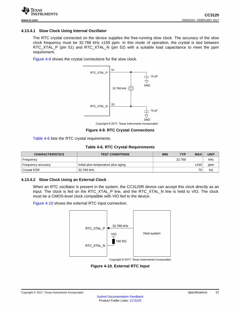
The RTC crystal connected on the device supplies the free-running slow clock. The accuracy of the slowclock frequency must be 32.768 kHz ±150 ppm. In this mode of operation, the crystal is tied betweenRTC_XTAL_P (pin 51) and RTC_XTAL_N (pin 52) with a suitable load capacitance to meet the ppmrequirement.
Figure 4-9 shows the crystal connections for the slow clock.
Figure 4-9. RTC Crystal Connections
Table 4-6 lists the RTC crystal requirements.
Table 4-6. RTC Crystal Requirements
CHARACTERISTICS TEST CONDITIONS MIN TYP MAX UNITFrequency 32.768 kHzFrequency accuracy Initial plus temperature plus aging ±150 ppmCrystal ESR 32.768 kHz 70 kΩ
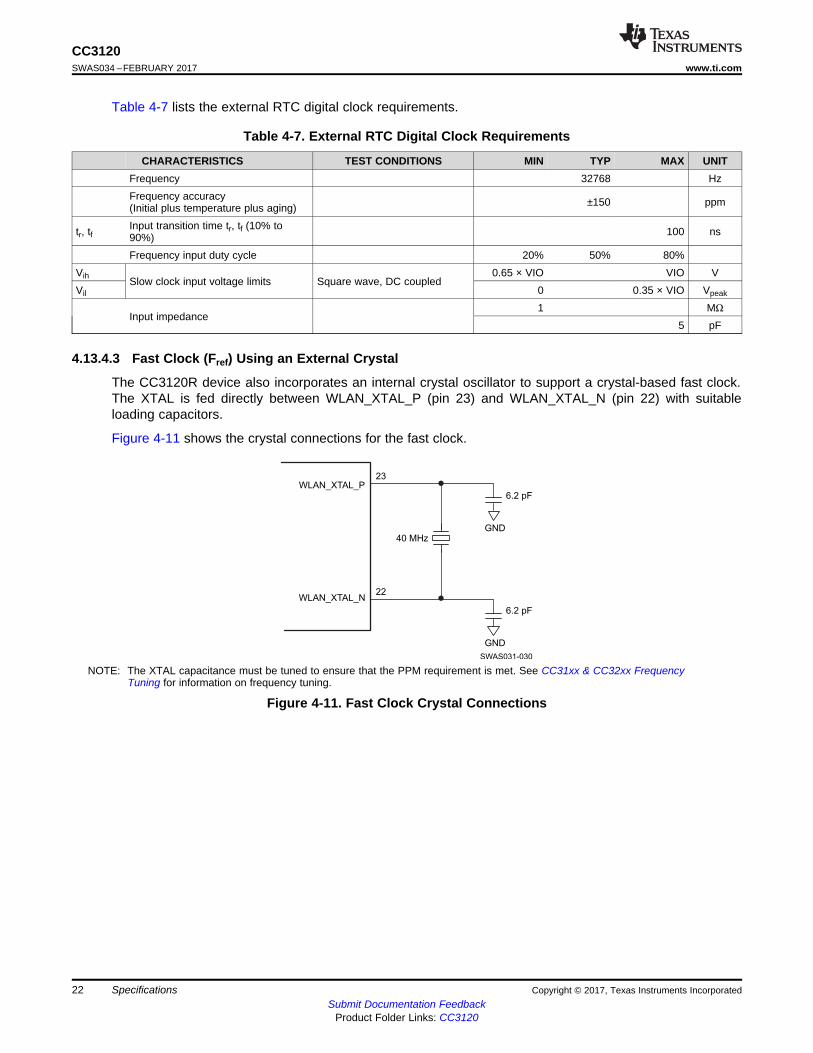
4.13.4.2 Slow Clock Using an External Clock
When an RTC oscillator is present in the system, the CC3120R device can accept this clock directly as aninput. The clock is fed on the RTC_XTAL_P line, and the RTC_XTAL_N line is held to VIO. The clockmust be a CMOS-level clock compatible with VIO fed to the device.
Figure 4-10 shows the external RTC input connection.
Table 4-7 lists the external RTC digital clock requirements.
Table 4-7. External RTC Digital Clock Requirements
CHARACTERISTICS TEST CONDITIONS MIN TYP MAX UNITFrequency 32768 HzFrequency accuracy(Initial plus temperature plus aging) ±150 ppm
tr, tfInput transition time tr, tf (10% to90%) 100 ns
Frequency input duty cycle 20% 50% 80%Vih Slow clock input voltage limits Square wave, DC coupled
0.65 × VIO VIO VVil 0 0.35 × VIO Vpeak
Input impedance1 MΩ
5 pF
4.13.4.3 Fast Clock (Fref) Using an External Crystal
The CC3120R device also incorporates an internal crystal oscillator to support a crystal-based fast clock.The XTAL is fed directly between WLAN_XTAL_P (pin 23) and WLAN_XTAL_N (pin 22) with suitableloading capacitors.
Figure 4-11 shows the crystal connections for the fast clock.
NOTE: The XTAL capacitance must be tuned to ensure that the PPM requirement is met. See CC31xx & CC32xx FrequencyTuning for information on frequency tuning.
Table 4-8 lists the WLAN fast-clock crystal requirements.
Table 4-8. WLAN Fast-Clock Crystal Requirements
CHARACTERISTICS TEST CONDITIONS MIN TYP MAX UNITFrequency 40 MHzFrequency accuracy Initial plus temperature plus aging ±25 ppmCrystal ESR 40 MHz 60 Ω
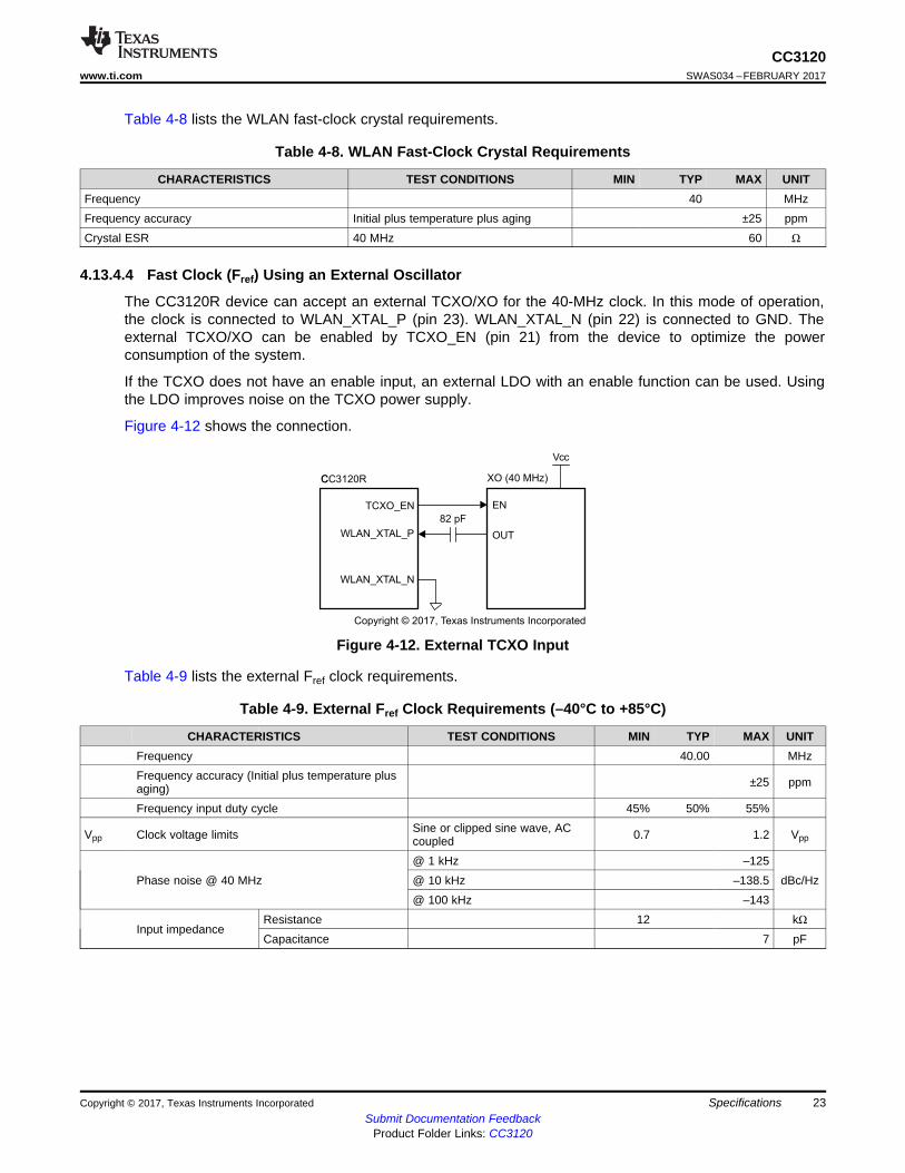
4.13.4.4 Fast Clock (Fref) Using an External Oscillator
The CC3120R device can accept an external TCXO/XO for the 40-MHz clock. In this mode of operation,the clock is connected to WLAN_XTAL_P (pin 23). WLAN_XTAL_N (pin 22) is connected to GND. Theexternal TCXO/XO can be enabled by TCXO_EN (pin 21) from the device to optimize the powerconsumption of the system.
If the TCXO does not have an enable input, an external LDO with an enable function can be used. Usingthe LDO improves noise on the TCXO power supply.
Figure 4-12 shows the connection.
Figure 4-12. External TCXO Input
Table 4-9 lists the external Fref clock requirements.
Table 4-9. External Fref Clock Requirements (–40°C to +85°C)
CHARACTERISTICS TEST CONDITIONS MIN TYP MAX UNITFrequency 40.00 MHzFrequency accuracy (Initial plus temperature plusaging) ±25 ppm
Frequency input duty cycle 45% 50% 55%
Vpp Clock voltage limits Sine or clipped sine wave, ACcoupled 0.7 1.2 Vpp
4.13.5 InterfacesThis section describes the interfaces that are supported by the CC3120R device:• Host SPI• Flash SPI
4.13.5.1 Host SPI Interface Timing
Figure 4-13 shows the Host SPI interface timing diagram.
Figure 4-13. Host SPI Interface Timing
Table 4-10 lists the Host SPI interface timing parameters.
(1) The timing parameter has a maximum load of 20 pF at 3.3 V.(2) Ensure that nCS (active-low signal) is asserted 10 ns before the clock is toggled. nCS can be deasserted 10 ns after the clock edge.
I1 F Clock frequency 20 MHzI2 tclk Clock period 50 nsI3 tLP Clock low period 25 nsI4 tHT Clock high period 25 nsI5 D Duty cycle 45% 55%I6 tIS RX data setup time 1 nsI7 tIH RX data hold time 2 nsI8 tOD TX data output delay 8.5 nsI9 tOH TX data hold time 8 ns
4.14.1 SPI Flash InterfaceThe external serial flash stores the user profiles and firmware patch updates. The CC3120R device actsas a master in this case; the SPI serial flash acts as the slave device. This interface can work up to aspeed of 20 MHz.
Figure 4-15 shows the SPI flash interface.
Figure 4-15. SPI Flash Interface
Table 4-12 lists the SPI flash interface pins.
Table 4-12. SPI Flash Interface
PIN NAME DESCRIPTIONFLASH_SPI_CLK Clock (up to 20 MHz) CC3120R device to serial flashFLASH_SPI_CS CS signal from CC3120R device to serial flashFLASH_SPI_MISO Data from serial flash to CC3120R deviceFLASH_SPI_MOSI Data from CC3120R device to serial flash
4.14.2 SPI Host InterfaceThe device interfaces to an external host using the SPI interface. The CC3120R device can interrupt thehost using the HOST_INTR line to initiate the data transfer over the interface. The SPI host interface canwork up to a speed of 20 MHz.
Figure 4-16 shows the SPI host interface.
Figure 4-16. SPI Host Interface
Table 4-13 lists the SPI host interface pins.
Table 4-13. SPI Host Interface
PIN NAME DESCRIPTIONHOST_SPI_CLK Clock (up to 20 MHz) from MCU host to CC3120R deviceHOST_SPI_nCS CS (active low) signal from MCU host to CC3120R deviceHOST_SPI_MOSI Data from MCU host to CC3120R deviceHOST_INTR Interrupt from CC3120R device to MCU hostHOST_SPI_MISO Data from CC3120R device to MCU host
nHIB Active-low signal that commands the CC3120R device to enter hibernate mode (lowestpower state)
(1) The SimpleLink device does not support automatic detection of the host length while using the UART interface.
4.15 Host UARTThe SimpleLink device requires the UART configuration described in Table 4-14.
Table 4-14. SimpleLink UART Configuration
PROPERTY SUPPORTED CC3120R CONFIGURATIONBaud rate 115200 bps, no auto-baud rate detection, can be changed by the host up to 3 Mbps using a special commandData bits 8 bitsFlow control CTS/RTSParity NoneStop bits 1Bit order LSBit firstHost interrupt polarity Active highHost interrupt mode Rising edge or level 1Endianness Little-endian only (1)
4.15.1 5-Wire UART TopologyFigure 4-17 shows the typical 5-wire UART topology comprised of four standard UART lines plus one IRQline from the device to the host controller to allow efficient low-power mode.
Figure 4-17. Typical 5-Wire UART Topology
This topology is recommended because the configuration offers the maximum communication reliabilityand flexibility between the host and the SimpleLink device.
4.15.2 4-Wire UART TopologyThe 4-wire UART topology eliminates the host IRQ line (see Figure 4-18). Using this topology requiresmeeting one of the following conditions:• The host is always awake or active.• The host goes to sleep, but the UART module has receiver start-edge detection for auto wakeup and
4.15.3 3-Wire UART TopologyThe 3-wire UART topology requires only the following lines (see Figure 4-19):• RX• TX• CTS
Figure 4-19. 3-Wire UART Topology
Using this topology requires meeting one of the following conditions:• The host always stays awake or active.• The host goes to sleep but the UART module has receiver start-edge detection for auto-wake-up and
does not lose data.• The host can always receive any amount of data transmitted by the SimpleLink device because there
is no flow control in this direction.
Because there is no full flow control, the host cannot stop the SimpleLink device to send its data; thus, thefollowing parameters must be carefully considered:• Maximum baud rate• RX character interrupt latency and low-level driver jitter buffer• Time consumed by the user's application
5.1 OverviewThe CC3120R Wi-Fi Internet-on-a-chip contains a dedicated ARM MCU that offloads many of thenetworking activities from the host MCU. The device includes an 802.11b/g/n radio, baseband, and MACwith a powerful crypto engine for a fast, secure WLAN and Internet connections with 256-bit encryption.The CC3120R device supports station, AP, and Wi-Fi Direct modes. The device also supports WPA2personal and enterprise security and WPS 2.0. The Wi-Fi network processor includes an embedded IPv6and IPv4 TCP/IP stack.
5.2 Functional Block DiagramFigure 5-1 shows the functional block diagram of the CC3120R SimpleLink Wi-Fi solution.
5.3.1 WLANThe WLAN features are as follows:• 802.11b/g/n integrated radio, modem, and MAC supporting WLAN communication as a BSS station,
AP, Wi-Fi Direct client and group owner with CCK and OFDM rates in the 2.4-GHz ISM band, channels1 to 13.
NOTE802.11n is supported only in Wi-Fi station, Wi-Fi direct, and P2P client mode
• Autocalibrated radio with a single-ended 50-Ω interface enables easy connection to the antennawithout requiring expertise in radio circuit design.
• Advanced connection manager with multiple user-configurable profiles stored in serial-flash allowsautomatic fast connection to an access point without user or host intervention.
• Supports all common Wi-Fi security modes for personal and enterprise networks with on-chip securityaccelerators, including: WEP, WPA/WPA2 PSK, WPA2 Enterprise (802.1x).
• Smart provisioning options deeply integrated within the device providing a comprehensive end-to-endsolution. With elaborate events notification to the host, enabling the application to control theprovisioning decision flow. The wide variety of Wi-Fi provisioning methods include:– Access Point using HTTPS– SmartConfig Technology: a 1-step, 1-time process to connect a CC3120R-enabled device to the
home wireless network, removing dependency on the I/O capabilities of the host MCU; thus, it isusable by deeply embedded applications
• 802.11 transceiver mode allows transmitting and receiving of proprietary data through a socket withoutadding MAC or PHY headers. The 802.11 transceiver mode provides the option to select the workingchannel, rate, and transmitted power. The receiver mode works with the filtering options.
5.3.2 Network StackThe Network Stack features are as follows:• Integrated IPv4, IPv6 TCP/IP stack with BSD (BSD adjacent) socket APIs for simple Internet
connectivity with any MCU, microprocessor, or ASIC
NOTENot all APIs are 100% BSD compliant. Not all BSD APIs are supported.
• Support of 16 simultaneous TCP, UDP, or RAW sockets• Support of 6 simultaneous SSL\TLS sockets• Built-in network protocols:
– Static IP, LLA, DHCPv4, DHCPv6 with DAD and stateless autoconfiguration– ARP, ICMPv4, IGMP, ICMPv6, MLD, ND– DNS client for easy connection to the local network and the Internet
• Built-in network application and utilities:– HTTP/HTTPS
• Web page content stored on serial flash• RESTful APIs for setting and configuring application content• Dynamic user callbacks
– Service discovery: Multicast DNS service discovery lets a client advertise its service without acentralized server. After connecting to the access point, the CC3120R device provides criticalinformation, such as device name, IP, vendor, and port number.
– DHCP server– Ping
Table 5-1 summarizes the NWP features.
Table 5-1. NWP Features
Feature Description
Wi-Fi standards802.11b/g/n station802.11b/g AP supporting up to four stationsWi-Fi Direct client and group owner
Wi-Fi Channels 1 to 13Wi-Fi security WEP, WPA/WPA2 PSK, WPA2 enterprise (802.1x)Wi-Fi provisioning SmartConfig technology, Wi-Fi protected setup (WPS2), AP mode with internal HTTP/HTTPS web serverIP protocols IPv4/IPv6IP addressing Static IP, LLA, DHCPv4, DHCPv6 (Stateful) with DAD and stateless auto configurationCross layer ARP, ICMPv4, IGMP, ICMPv6, MLD, NDP
TransportUDP, TCPSSLv3.0/TLSv1.0/TLSv1.1/TLSv1.2RAW IP
Network applications andutilities
PingHTTP/HTTPS web servermDNSDNS-SDDHCP server
Host interface UART/SPI
SecurityDevice identityTrusted root-certificate catalogTI root-of-trust public key
Power management Enhanced power policy management uses 802.11 power save and deep sleep power modes
OtherRF TransceiverProgrammable RX Filters with Events trigger mechanism including WoWLANRecovery mechanism – Restore to factory default
5.3.3 SecurityThe SimpleLink Wi-Fi CC3120R Internet-on-a-chip device enhances the security capabilities available fordevelopment of IoT devices, while completely offloading these activities from the MCU to the networkingsubsystem. The security capabilities include the following key features:
Wi-Fi and Internet Security:• Personal and enterprise Wi-Fi security
– Personal standards• AES (WPA2-PSK)• TKIP (WPA-PSK• WEP
– Server authentication– Client authentication– Domain name verification– Socket upgrade to secure socket – STARTTLS
• Secure HTTP server (HTTPS)• The Trusted root-certificate catalog verifies that the CA used by the application is trusted and known
secure content delivery• The TI root-of-trust public key is a hardware-based mechanism that allows authenticating TI as the
genuine origin of a given content using asymmetric keys• Secure content delivery allows file transfer to the system in a secure way on any unsecured tunnel
Code and Data Security:• Secured network information: Network passwords and certificates are encrypted• Secured and authenticated service pack: SP is signed based on TI certificate
5.3.4 Host Interface and Driver• Interfaces over a 4-wire serial peripheral interface (SPI) with any MCU or a processor at a clock speed
of 20 MHz.• Interfaces over UART with any MCU with a baud rate up to 3 Mbps. A low footprint driver is provided
for TI MCUs and is easily ported to any processor or ASIC.• Simple APIs enable easy integration with any single-threaded or multithreaded application.
5.3.5 System• Works from a single preregulated power supply or connects directly to a battery• Ultra-low leakage when disabled (hibernate mode) with a current of less than 4 µA with the RTC
5.4 Power-Management SubsystemThe CC3120R power-management subsystem contains DC-DC converters to accommodate the differentvoltage or current requirements of the system.• Digital DC-DC (Pin 44)
– Input: VBAT wide voltage (2.1 to 3.6 V) or preregulated 1.85 V• ANA1 DC-DC (Pin 38)
– Input: VBAT wide voltage (2.1 to 3.6 V)– In preregulated 1.85-V mode, the ANA1 DC-DC converter is bypassed.
• PA DC-DC (Pin 39)– Input: VBAT wide voltage (2.1 to 3.6 V)– In preregulated 1.85-V mode, the PA DC-DC converter is bypassed.
The CC3120R device is a single-chip WLAN radio solution used on an embedded system with a wide-voltage supply range. The internal power management, including DC-DC converters and LDOs, generatesall of the voltages required for the device to operate from a wide variety of input sources. For maximumflexibility, the device can operate in the modes described in Section 5.4.1 and Section 5.4.2.
5.4.1 VBAT Wide-Voltage ConnectionIn the wide-voltage battery connection, the device is powered directly by the battery or preregulated 3.3-Vsupply. All other voltages required to operate the device are generated internally by the DC-DCconverters. This scheme supports wide-voltage operation from 2.1 to 3.6 V and is thus the most commonmode for the device.
5.4.2 Preregulated 1.85VThe preregulated 1.85-V mode of operation applies an external regulated 1.85 V directly at pins 10, 25,33, 36, 37, 39, 44, 48, and 54 of the device. The VBAT and the VIO are also connected to the 1.85-Vsupply. This mode provides the lowest BOM count version in which inductors used for PA DC-DC andANA1 DC-DC (2.2 and 1 µH) and a capacitor (22 µF) can be avoided.
In the preregulated 1.85-V mode, the regulator providing the 1.85 V must have the followingcharacteristics:• Load current capacity ≥900 mA• Line and load regulation with <2% ripple with 500-mA step current and settling time of < 4 µs with the
load step
NOTEThe regulator must be placed as close as possible to the device so that the IR drop to thedevice is very low.
5.5 Low-Power Operating ModesThis section describes the low-power modes supported by the device to optimize battery life.
5.5.1 Low-Power Deep SleepThe low-power deep-sleep (LPDS) mode is an energy-efficient and transparent sleep mode that is enteredautomatically during periods of inactivity based on internal power optimization algorithms. The device canwake up in less than 3 ms from the internal timer or from any incoming host command. Typical batterydrain in this mode is 115 µA. During LPDS mode, the device retains the software state and certainconfiguration information. The operation is transparent to the external host; thus, no additional handshakeis required to enter or exit LPDS mode.
5.5.2 HibernateThe hibernate mode is the lowest power mode in which all of the digital logic is power-gated. Only a smallsection of the logic powered directly by the main input supply is retained. The RTC is kept running and thedevice wakes up once the nHIB line is asserted by the host driver. The wake-up time is longer than LPDSmode at approximately 50 ms.
NOTEWake-up time can be extended depending on the service-pack size.
5.5.3 ShutdownThe shutdown mode is the lowest power-mode system-wise. All device logics are off, including the real-time clock (RTC). The wake-up time in this mode is longer than hibernate at approximately 1.1 s.
5.6.1 External Memory RequirementsThe CC3120R device maintains a proprietary file system on the sFLASH. The CC3120R file system storesthe service pack file, system files, configuration files, certificate files, web page files, and user files. Byusing a format command through the API, users can provide the total size allocated for the file system.The starting address of the file system cannot be set and is always at the beginning of the sFLASH. Theapplications microcontroller must access the sFLASH memory area allocated to the file system directlythrough the CC3120R file system. The applications microcontroller must not access the sFLASH memoryarea directly.
The file system manages the allocation of sFLASH blocks for stored files according to download order,which means that the location of a specific file is not fixed in all systems. Files are stored on sFLASHusing human-readable filenames rather than file IDs. The file system API works using plain text, and fileencryption and decryption is invisible to the user. Encrypted files can be accessed only through the filesystem.
All file types can have a maximum of 100 supported files in the file system. All files are stored in 4-KBblocks and thus use a minimum of 4KB of flash space. Fail-safe files require twice the original size anduse a minimum of 8KB. Encrypted files are counted as fail-safe in terms of space. The maximum file sizeis 1MB.
Table 5-2 lists the minimum required memory consumption under the following assumptions:• System files in use consume 64 blocks (256KB).• Vendor files are not taken into account.• Gang image:
– Storage for the gang image is rounded up to 32 blocks (meaning 128-KB resolution).– Gang image size depends on the actual content size of all components. Additionally, the image
should be 128-KB aligned so unaligned memory is considered lost. Service pack, system files, andthe 128-KB aligned memory are assumed to occupy 256KB.
• All calculations consider that the restore-to-default is enabled.
NOTEThe maximum supported sFLASH size is 32MB (256Mb). Please refer to Using Serial Flashon CC3120/CC3220 SimpleLink™ Wi-Fi® and Internet-of-Things Devices.
5.7 Restoring Factory Default ConfigurationThe device has an internal recovery mechanism that allows rolling back the file system to its predefinedfactory image or restoring the factory default parameters of the device. The factory image is kept in aseparate sector on the sFLASH in a secure manner and cannot be accessed from the host processor. Thefollowing restore modes are supported:• None—no factory restore settings• Enable restore of factory default parameters• Enable restore of factory image and factory default parameters
The restore process is performed by pulling or forcing SOP[2:0] = 110 pins and toggling the nRESET pinfrom low to high.
The process is fail-safe and resumes operation if a power failure occurs before the restore is finished. Therestore process typically takes about 8 seconds, depending on the attributes of the serial flash vendor.
NOTEInformation in the following Applications section is not part of the TI component specification,and TI does not warrant its accuracy or completeness. TI's customers are responsible fordetermining suitability of components for their purposes. Customers should validate and testtheir design implementation to confirm system functionality.
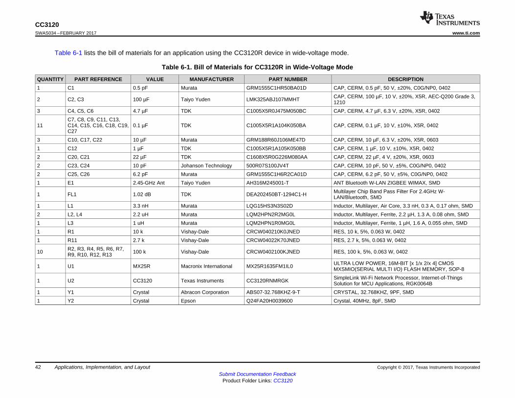
Figure 6-1 shows the typical application schematic using the CC3120R device in the wide-voltage mode of operation. For a full operation referencedesign, refer to the BoosterPack that uses the CC3120R device (see CC3120 SimpleLink™ and Internet of Things Hardware Design Files).
6.1.2 Typical Application Schematic—CC3120R Preregulated, 1.85-V ModeFigure 6-2 shows the typical application schematic using the CC3120R in preregulated, 1.85-V mode of operation. For addition information on thismode of operation please contact your TI representative.
6.2 PCB Layout GuidelinesThis section details the PCB guidelines to speed up the PCB design using the CC3120R VQFN device.Follow these guidelines ensures that the design will minimize the risk with regulatory certificationsincluding FCC, ETSI, and CE. For more information, see CC3120 and CC3220 SimpleLink™ Wi-Fi® andIoT Solution Layout Guidelines.
6.2.1 General PCB GuidelinesUse the following PCB guidelines:• Verify the recommended PCB stackup in the PCB design guidelines, as well as the recommended
layers for signals and ground.• Ensure that the QFN PCB footprint follows the information in Section 8.• Ensure that the QFN PCB GND and solder paste follow the recommendations provided in CC3120 and
CC3220 SimpleLink™ Wi-Fi® and IoT Solution Layout Guidelines.• Decoupling capacitors must be as close as possible to the QFN device.
6.2.2 Power Layout and RoutingThree critical DC-DC converters must be considered for the CC3120R device.• Analog DC-DC converter• PA DC-DC converter• Digital DC-DC converter
Each converter requires an external inductor and capacitor that must be laid out with care. DC currentloops are formed when laying out the power components.
6.2.2.1 Design Considerations
The following design guidelines must be followed when laying out the CC3120R device:• Route all of the input decoupling capacitors (C11, C13, and C18) on L2 using thick traces, to isolate
the RF ground from the noisy supply ground. This step is also required to meet the IEEE spectral maskspecifications.
• Maintain the thickness of power traces to be greater than 12 mils. Take special consideration for poweramplifier supply lines (pin 33, 40, 41, and 42), and all input supply pins (pin 37, 39, and 44).
• Ensure the shortest grounding loop for the PLL supply decoupling capacitor (pin 24).• Place all decoupling capacitors as close to the respective pins as possible.• Power budget: The CC3120R device can consume up to 450 mA for 3.3 V, 670 mA for 2.1 V, and 700
mA for 1.85 V, for 24 ms during the calibration cycle.• Ensure the power supply is designed to source this current without any issues. The complete
calibration (TX and RX) can take up to 17 mJ of energy from the battery over a time of 24 ms.• The CC3120R device contains many high-current input pins. Ensure the trace feeding these pins is
capable of handling the following currents:– PA DCDC input (pin 39) maximum 1 A– ANA DCDC input (pin 37) maximum 600 mA– DIG DCDC input (pin 44) maximum 500 mA– PA DCDC switching nodes (pin 40 and pin 41) maximum 1 A– PA DCDC output node (pin 42) maximum 1 A– ANA DCDC switching node (pin 38) maximum 600 mA– DIG DCDC switching node (pin 43) maximum 500 mA– PA supply (pin 33) maximum 500 mA
Figure 6-3 shows the ground routing for the input decoupling capacitors.
Figure 6-3. Ground Routing for the Input Decoupling Capacitors
The ground return for the input capacitors are routed on L2 to reduce the EMI and improve the spectralmask. This routing must be strictly followed because it is critical for the overall performance of the device.
6.2.3 Clock InterfacesThe following guidelines are for the slow clock.• The 32.768-kHz crystal must be placed close to the QFN package.• Ensure that the load capacitance is tuned according to the board parasitics to the frequency tolerance
is within ±150 ppm.• The ground plane on layer two is solid below the trace lanes and there is ground around these traces
on the top layer.
The following guidelines are for the fast clock.• The 40-MHz crystal must be placed close to the QFN package.• Ensure that he load capacitance is tuned according to the board parasitics to the frequency tolerance
is within ±100 ppm at room temperature. The total frequency across parts, temperature, and withaging, must be ±25 ppm to meet the WLAN specification.
• Ensure that no high-frequency lines are routed close to the XTAL routing to avoid noise degradation.• Ensure that crystal tuning capacitors are close to the crystal pads.• Make both traces (XTALM and XTALP) as close to parallel as possible and approximately the same
length.• The ground plane on layer two is solid below the trace lines and that there is ground around these
traces on the top layer.• See CC31xx & CC32xx Frequency Tuning for frequency tuning.
6.2.4 Digital Input and OutputThe following guidelines are for the digital I/O.• Route SPI and UART lines away from any RF traces.• Keep the length of the high-speed lines as short as possible to avoid transmission line effects.• Keep the line lower than 1/10 of the rise time of the signal to ignore transmission line effects. This is
required if the traces cannot be kept short. Place the resistor at the source end, closer to the devicethat is driving the signal.
• Add series-terminating resistor for each high-speed line (such as SPI_CLK or SPI_DATA) to match thedriver impedance to the line. Typical terminating-resistor values range from 27 to 36 Ω for a 50-Ω lineimpedance.
• Route high-speed lines with a ground reference plane continuously below it to offer good impedancethroughout. This routing also helps shield the trace against EMI.
• Avoid stubs on high-speed lines to minimize the reflections. If the line must be routed to multiplelocations, use a separate line driver for each line.
• If the lines are longer compared to the rise time, add series-terminating resistors near the driver foreach high-speed line to match the driver impedance to the line. Typical terminating-resistor valuesrange from 27 to 36 Ω for a 50-Ω line impedance.
6.2.5 RF InterfaceThe following guidelines are for the RF interface. Follow guidelines specified in the vendor-specificantenna design guides (including placement of the antenna). Also see CC3120 and CC3220 SimpleLink™Wi-Fi® and IoT Solution Layout Guidelines for general antenna guidelines.• Ensure that the antenna is matched for 50-Ω. A Pi-matching network is recommended.• Ensure that the area underneath the BPF pads are grounded on layer one and layer two, and that the
minimum fulter requirements are met.• Verify that the Wi-Fi RF trace is a 50-Ω, impedance-controlled trace with a reference to solid ground.• The RF trace bends must be made with gradual curves, and 90-degree bends must be avoided.• The RF traces must not have sharp corners.• There must be no traces or ground under the antenna section.• The RF traces must have via stitching on the ground plane beside the RF trace on both sides.
TI offers an extensive line of development tools. Tools and software to evaluate the performance of thedevice, generate code, and develop solutions are listed in this section.
7.1 Tools and SoftwareDevelopment ToolsSimpleLink Studio for CC3120R The CC3120R device is supported.
SimpleLink Studio for CC3120R is a Windows®-based software tool used to aid in thedevelopment of embedded networking applications and software for microcontrollers. UsingSimpleLink Studio for CC3120R, embedded software developers can develop and testapplications using any desktop IDE, such as Visual Studio or Eclipse, and connect theirapplications to the cloud using the CC3120R BoosterPack™ Plug-in Module. The applicationcan then be easily ported to any microcontroller. With the SimpleLink Wi-Fi CC3120Rsolution, customers now have the flexibility to add Wi-Fi to any microcontroller (MCU). ThisInternet-on-a-chip solution contains all you need to easily create IoT solutions: security, quickconnection, cloud support, and more. For more information on CC3120R, visit SimpleLinkWi-Fi Solutions.
CC3120R Software Development Kit (SDK) The CC3120R device is supported.The SimpleLink Wi-Fi CC3220 SDK contains drivers for the CC3220 programmable MCU,30+ sample applications, and documentation needed to use the solution. The SDK alsocontains the flash programmer, a command line tool for flashing software, configuringnetwork and software parameters (SSID, access point channel, network profile, and so on),system files, and user files (certificates, web pages, and so on). This SDK can be used withTI’s SimpleLInk Wi-Fi CC3220 LaunchPad™ development kit.The SDK has a variety of support offerings. All sample applications in the SDK aresupported on the integrated Cortex-M4 processor with CCS IDE and no RTOS. In addition, afew of the applications support IAR, Free RTOS, and TI-RTOS.
TI Designs and Reference Designs
The TI Designs Reference Design Library is a robust reference design library spanning analog, embeddedprocessor, and connectivity. Created by TI experts to help you jumpstart your system design, all TIDesigns include schematic or block diagrams, BOMs, and design files to speed your time to market.
7.2 Device NomenclatureTo designate the stages in the product development cycle, TI assigns prefixes to the part numbers of theCC3120R device and support tools (see Figure 7-1).
Figure 7-1. CC3120R Device Nomenclature
7.3 Documentation SupportTo receive notification of documentation updates—including silicon errata—go to the product folder foryour device on ti.com (CC3120). In the upper right corner, click the "Alert me" button. This registers you toreceive a weekly digest of product information that has changed (if any). For change details, check therevision history of any revised document. The current documentation that describes the processor, relatedperipherals, and other technical collateral follows.
The following documents provide support for the CC3120 device.
Application ReportsSimpleLink™ CC3120, CC3220 Wi-Fi® Internet-on-a chip™ Networking Sub-System Power
ManagementThis application report describes the best practices for power management and extendedbattery life for embedded low-power Wi-Fi devices such as the SimpleLink Wi-Fi Internet-on-a chip™ solution from Texas Instruments™.
SimpleLink™ CC3120, CC3220 Wi-Fi® Internet-on-a chip™ Solution Built-In Security Features TheSimpleLink Wi-Fi CC3120 and CC3220 Internet-on-a chip™ family of devices from TexasInstruments™ offer a wide range of built-in security features to help developers address avariety of security needs, which is achieved without any processing burden on the mainmicrocontroller (MCU). This document describes these security-related features and providesrecommendations for leveraging each in the context of practical system implementation.
SimpleLink™ CC3120, CC3220 Wi-Fi® and Internet of Things Over-the-Air Update This documentdescribes the OTA library for the SimpleLink™ Wi-Fi® CC3x20 family of devices from TexasInstruments™ and explains how to prepare a new cloud-ready update to be downloaded bythe OTA library.
SimpleLink™ CC3120, CC3220 Wi-Fi® Internet-on-a chip™ Solution Device Provisioning This guidedescribes the provisioning process, which provides the SimpleLink Wi-Fi device with theinformation (network name, password, and so forth) needed to connect to a wirelessnetwork.
Using Serial Flash on SimpleLink™ CC3120 and CC3220 Wi-Fi® and Internet-of-Things DevicesThis application note is divided into two parts. The first part provides important guidelinesand best- practice design techniques to consider when choosing and embedding a serialflash paired with the CC3120 and CC3220 (CC3x20) devices. The second part describes thefile system, along with guidelines and considerations for system designers working with theCC3x20 devices.
User's GuidesSimpleLink™ Wi-Fi® and Internet of Things CC3120 and CC3220 Network Processor This document
provides software (SW) programmers with all of the required knowledge for working with thenetworking subsystem of the SimpleLink Wi-Fi devices. This guide provides basic guidelinesfor writing robust, optimized networking host applications, and describes the capabilities ofthe networking subsystem. The guide contains some example code snapshots, to give usersan idea of how to work with the host driver. More comprehensive code examples can befound in the formal software development kit (SDK). This guide does not provide a detaileddescription of the host driver APIs.
SimpleLink™ Wi-Fi® CC3120 BoosterPack™ Plug-In Module and IoT SolutionThe SimpleLink Wi-FiCC3120 wireless network processor from Texas Instruments™ provides users the flexibilityto add Wi-Fi to any MCU. This user's guide explains the various configurations of theCC3120 BoosterPack™ Plug-In Module.
SimpleLink™ Wi-Fi® CC3120 and CC3220 and IoT Solution Layout Guidelines This documentprovides the design guidelines of the 4-layer PCB used for the CC3120 and CC3220SimpleLink Wi-Fi family of devices from Texas Instruments™. The CC3120 and CC3220devices are easy to lay out and are available in quad flat no-leads (QFNS) packages. Whendesigning the board, follow the suggestions in this document to optimize performance of theboard.
SimpleLink™ Wi-Fi® CC3120 Internet-on-a-chip™ Solution SDKThis guide is intended to help users inthe initial setup and demonstration of the different demos in the CC3120 SDK. The guidelists the software and hardware components required to get started, and explains how toinstall the supported integrated development environment (IDE), SimpleLink CC3120 SDK,and the various other tools required.
SimpleLink™ Wi-Fi® and Internet-on-a-chip™ CC3120 and CC3220 Solution Radio Tool The RadioTool serves as a control panel for direct access to the radio, and can be used for both theradio frequency (RF) evaluation and for certification purposes. This guide describes how tohave the tool work seamlessly on Texas Instruments ™ evaluation platforms such as theBoosterPack™ plus FTDI emulation board for CC3120 devices, and the LaunchPad™ forCC3220 devices.
SimpleLink™ Wi-Fi® CC3120 and CC3220 Provisioning for Mobile Applications This guide describesTI’s SimpleLink™ Wi-Fi® provisioning solution for mobile applications, specifically on theusage of the Android™ and iOS® building blocks for UI requirements, networking, andprovisioning APIs required for building the mobile application.
More LiteratureRemoTI ManifestCC3120 SimpleLink™ WI-Fi® and Internet of Things CC3120 hardware design files.
7.4 Community ResourcesThe following links connect to TI community resources. Linked contents are provided "AS IS" by therespective contributors. They do not constitute TI specifications and do not necessarily reflect TI's views;see TI's Terms of Use.TI E2E™ Online Community The TI engineer-to-engineer (E2E) community was created to foster
collaboration among engineers. At e2e.ti.com, you can ask questions, share knowledge,explore ideas and help solve problems with fellow engineers.
TI Embedded Processors Wiki Established to help developers get started with Embedded Processorsfrom Texas Instruments and to foster innovation and growth of general knowledge about thehardware and software surrounding these devices.
7.5 TrademarksSimpleLink, Internet-on-a chip, SmartConfig, Texas Instruments, E2E, BoosterPack, LaunchPad aretrademarks of Texas Instruments.Cortex is a registered trademark of ARM Limited.ARM is a registered trademark of ARM Physical IP, Inc.Bluetooth is a registered trademark of Bluetooth SIG, Inc.Windows is a registered trademark of Microsoft Inc.Wi-Fi, Wi-Fi Direct are registered trademarks of Wi-Fi Alliance.All other trademarks are the property of their respective owners.
7.6 Electrostatic Discharge CautionThis integrated circuit can be damaged by ESD. Texas Instruments recommends that all integrated circuits be handled withappropriate precautions. Failure to observe proper handling and installation procedures can cause damage.
ESD damage can range from subtle performance degradation to complete device failure. Precision integrated circuits may be moresusceptible to damage because very small parametric changes could cause the device not to meet its published specifications.
7.7 Export Control NoticeRecipient agrees to not knowingly export or re-export, directly or indirectly, any product or technical data(as defined by the U.S., EU, and other Export Administration Regulations) including software, or anycontrolled product restricted by other applicable national regulations, received from disclosing party undernondisclosure obligations (if any), or any direct product of such technology, to any destination to whichsuch export or re-export is restricted or prohibited by U.S. or other applicable laws, without obtaining priorauthorization from U.S. Department of Commerce and other competent Government authorities to theextent required by those laws.
7.8 GlossaryTI Glossary This glossary lists and explains terms, acronyms, and definitions.
8 Mechanical, Packaging, and Orderable Information
The following pages include mechanical, packaging, and orderable information. This information is themost current data available for the designated devices. This data is subject to change without notice andrevision of this document. For browser-based versions of this data sheet, refer to the left-hand navigation.
CC3120RNMARGKR ACTIVE VQFN RGK 64 2500 Green (RoHS& no Sb/Br)
CU NIPDAU |CU NIPDAUAG
Level-3-260C-168 HR -40 to 85 CC3120RNMA
CC3120RNMARGKT ACTIVE VQFN RGK 64 250 Green (RoHS& no Sb/Br)
CU NIPDAU |CU NIPDAUAG
Level-3-260C-168 HR -40 to 85 CC3120RNMA
(1) The marketing status values are defined as follows:ACTIVE: Product device recommended for new designs.LIFEBUY: TI has announced that the device will be discontinued, and a lifetime-buy period is in effect.NRND: Not recommended for new designs. Device is in production to support existing customers, but TI does not recommend using this part in a new design.PREVIEW: Device has been announced but is not in production. Samples may or may not be available.OBSOLETE: TI has discontinued the production of the device.
(2) Eco Plan - The planned eco-friendly classification: Pb-Free (RoHS), Pb-Free (RoHS Exempt), or Green (RoHS & no Sb/Br) - please check http://www.ti.com/productcontent for the latest availabilityinformation and additional product content details.TBD: The Pb-Free/Green conversion plan has not been defined.Pb-Free (RoHS): TI's terms "Lead-Free" or "Pb-Free" mean semiconductor products that are compatible with the current RoHS requirements for all 6 substances, including the requirement thatlead not exceed 0.1% by weight in homogeneous materials. Where designed to be soldered at high temperatures, TI Pb-Free products are suitable for use in specified lead-free processes.Pb-Free (RoHS Exempt): This component has a RoHS exemption for either 1) lead-based flip-chip solder bumps used between the die and package, or 2) lead-based die adhesive used betweenthe die and leadframe. The component is otherwise considered Pb-Free (RoHS compatible) as defined above.Green (RoHS & no Sb/Br): TI defines "Green" to mean Pb-Free (RoHS compatible), and free of Bromine (Br) and Antimony (Sb) based flame retardants (Br or Sb do not exceed 0.1% by weightin homogeneous material)
(3) MSL, Peak Temp. - The Moisture Sensitivity Level rating according to the JEDEC industry standard classifications, and peak solder temperature.
(4) There may be additional marking, which relates to the logo, the lot trace code information, or the environmental category on the device.
(5) Multiple Device Markings will be inside parentheses. Only one Device Marking contained in parentheses and separated by a "~" will appear on a device. If a line is indented then it is a continuationof the previous line and the two combined represent the entire Device Marking for that device.
(6) Lead/Ball Finish - Orderable Devices may have multiple material finish options. Finish options are separated by a vertical ruled line. Lead/Ball Finish values may wrap to two lines if the finishvalue exceeds the maximum column width.
Important Information and Disclaimer:The information provided on this page represents TI's knowledge and belief as of the date that it is provided. TI bases its knowledge and belief on informationprovided by third parties, and makes no representation or warranty as to the accuracy of such information. Efforts are underway to better integrate information from third parties. TI has taken andcontinues to take reasonable steps to provide representative and accurate information but may not have conducted destructive testing or chemical analysis on incoming materials and chemicals.TI and TI suppliers consider certain information to be proprietary, and thus CAS numbers and other limited information may not be available for release.
In no event shall TI's liability arising out of such information exceed the total purchase price of the TI part(s) at issue in this document sold by TI to Customer on an annual basis.
VQFN - 1 mm max heightRGK0064BPLASTIC QUAD FLATPACK - NO LEAD
4222201/B 03/2018
0.08 C
0.1 C A B0.05
NOTES: 1. All linear dimensions are in millimeters. Any dimensions in parenthesis are for reference only. Dimensioning and tolerancing per ASME Y14.5M. 2. This drawing is subject to change without notice. 3. The package thermal pad must be soldered to the printed circuit board for thermal and mechanical performance.
PIN 1 INDEX AREA
SEATING PLANE
PIN 1 ID
SYMM
EXPOSEDTHERMAL PAD
SYMM
1
1617 32
33
484964
65
SCALE 1.500
AB
www.ti.com
EXAMPLE BOARD LAYOUT
60X (0.5)
( 0.2) TYPVIA
(R0.05) TYP
0.07 MAXALL AROUND
0.07 MINALL AROUND
64X (0.6)
64X (0.24)
(8.8)
(8.8)
( 6.3)
(0.6) TYP
18X (1.2)
8X (1.1)
(0.6) TYP
18X (1.2)8X
(1.1)
VQFN - 1 mm max heightRGK0064BPLASTIC QUAD FLATPACK - NO LEAD
4222201/B 03/2018
NOTES: (continued) 4. This package is designed to be soldered to a thermal pad on the board. For more information, see Texas Instruments literature number SLUA271 (www.ti.com/lit/slua271).5. Vias are optional depending on application, refer to device data sheet. If any vias are implemented, refer to their locations shown on this view. It is recommended that vias under paste be filled, plugged or tented.
SYMM
SYMM
LAND PATTERN EXAMPLEEXPOSED METAL SHOWN
SCALE: 10X
SEE SOLDER MASKDETAIL
1
16
17 32
33
48
4964
65
METAL EDGE
SOLDER MASKOPENING
EXPOSED METAL
METAL UNDERSOLDER MASK
SOLDER MASKOPENING
EXPOSEDMETAL
NON SOLDER MASKDEFINED
(PREFERRED)SOLDER MASK DEFINED
SOLDER MASK DETAILS
www.ti.com
EXAMPLE STENCIL DESIGN
64X (0.6)
64X (0.24)
60X (0.5)
(8.8)
(8.8)
25X ( 1)
(R0.05) TYP
(1.2) TYP
(1.2) TYP
VQFN - 1 mm max heightRGK0064BPLASTIC QUAD FLATPACK - NO LEAD
4222201/B 03/2018
NOTES: (continued) 6. Laser cutting apertures with trapezoidal walls and rounded corners may offer better paste release. IPC-7525 may have alternate design recommendations.
SOLDER PASTE EXAMPLEBASED ON 0.1 MM THICK STENCIL
SCALE: 10X
EXPOSED PAD 6563% PRINTED SOLDER COVERAGE BY AREA UNDER PACKAGE
SYMM
SYMM
1
16
17 32
33
48
4964
65
METALTYP
IMPORTANT NOTICE
Texas Instruments Incorporated (TI) reserves the right to make corrections, enhancements, improvements and other changes to itssemiconductor products and services per JESD46, latest issue, and to discontinue any product or service per JESD48, latest issue. Buyersshould obtain the latest relevant information before placing orders and should verify that such information is current and complete.TI’s published terms of sale for semiconductor products (http://www.ti.com/sc/docs/stdterms.htm) apply to the sale of packaged integratedcircuit products that TI has qualified and released to market. Additional terms may apply to the use or sale of other types of TI products andservices.Reproduction of significant portions of TI information in TI data sheets is permissible only if reproduction is without alteration and isaccompanied by all associated warranties, conditions, limitations, and notices. TI is not responsible or liable for such reproduceddocumentation. Information of third parties may be subject to additional restrictions. Resale of TI products or services with statementsdifferent from or beyond the parameters stated by TI for that product or service voids all express and any implied warranties for theassociated TI product or service and is an unfair and deceptive business practice. TI is not responsible or liable for any such statements.Buyers and others who are developing systems that incorporate TI products (collectively, “Designers”) understand and agree that Designersremain responsible for using their independent analysis, evaluation and judgment in designing their applications and that Designers havefull and exclusive responsibility to assure the safety of Designers' applications and compliance of their applications (and of all TI productsused in or for Designers’ applications) with all applicable regulations, laws and other applicable requirements. Designer represents that, withrespect to their applications, Designer has all the necessary expertise to create and implement safeguards that (1) anticipate dangerousconsequences of failures, (2) monitor failures and their consequences, and (3) lessen the likelihood of failures that might cause harm andtake appropriate actions. Designer agrees that prior to using or distributing any applications that include TI products, Designer willthoroughly test such applications and the functionality of such TI products as used in such applications.TI’s provision of technical, application or other design advice, quality characterization, reliability data or other services or information,including, but not limited to, reference designs and materials relating to evaluation modules, (collectively, “TI Resources”) are intended toassist designers who are developing applications that incorporate TI products; by downloading, accessing or using TI Resources in anyway, Designer (individually or, if Designer is acting on behalf of a company, Designer’s company) agrees to use any particular TI Resourcesolely for this purpose and subject to the terms of this Notice.TI’s provision of TI Resources does not expand or otherwise alter TI’s applicable published warranties or warranty disclaimers for TIproducts, and no additional obligations or liabilities arise from TI providing such TI Resources. TI reserves the right to make corrections,enhancements, improvements and other changes to its TI Resources. TI has not conducted any testing other than that specificallydescribed in the published documentation for a particular TI Resource.Designer is authorized to use, copy and modify any individual TI Resource only in connection with the development of applications thatinclude the TI product(s) identified in such TI Resource. NO OTHER LICENSE, EXPRESS OR IMPLIED, BY ESTOPPEL OR OTHERWISETO ANY OTHER TI INTELLECTUAL PROPERTY RIGHT, AND NO LICENSE TO ANY TECHNOLOGY OR INTELLECTUAL PROPERTYRIGHT OF TI OR ANY THIRD PARTY IS GRANTED HEREIN, including but not limited to any patent right, copyright, mask work right, orother intellectual property right relating to any combination, machine, or process in which TI products or services are used. Informationregarding or referencing third-party products or services does not constitute a license to use such products or services, or a warranty orendorsement thereof. Use of TI Resources may require a license from a third party under the patents or other intellectual property of thethird party, or a license from TI under the patents or other intellectual property of TI.TI RESOURCES ARE PROVIDED “AS IS” AND WITH ALL FAULTS. TI DISCLAIMS ALL OTHER WARRANTIES ORREPRESENTATIONS, EXPRESS OR IMPLIED, REGARDING RESOURCES OR USE THEREOF, INCLUDING BUT NOT LIMITED TOACCURACY OR COMPLETENESS, TITLE, ANY EPIDEMIC FAILURE WARRANTY AND ANY IMPLIED WARRANTIES OFMERCHANTABILITY, FITNESS FOR A PARTICULAR PURPOSE, AND NON-INFRINGEMENT OF ANY THIRD PARTY INTELLECTUALPROPERTY RIGHTS. TI SHALL NOT BE LIABLE FOR AND SHALL NOT DEFEND OR INDEMNIFY DESIGNER AGAINST ANY CLAIM,INCLUDING BUT NOT LIMITED TO ANY INFRINGEMENT CLAIM THAT RELATES TO OR IS BASED ON ANY COMBINATION OFPRODUCTS EVEN IF DESCRIBED IN TI RESOURCES OR OTHERWISE. IN NO EVENT SHALL TI BE LIABLE FOR ANY ACTUAL,DIRECT, SPECIAL, COLLATERAL, INDIRECT, PUNITIVE, INCIDENTAL, CONSEQUENTIAL OR EXEMPLARY DAMAGES INCONNECTION WITH OR ARISING OUT OF TI RESOURCES OR USE THEREOF, AND REGARDLESS OF WHETHER TI HAS BEENADVISED OF THE POSSIBILITY OF SUCH DAMAGES.Unless TI has explicitly designated an individual product as meeting the requirements of a particular industry standard (e.g., ISO/TS 16949and ISO 26262), TI is not responsible for any failure to meet such industry standard requirements.Where TI specifically promotes products as facilitating functional safety or as compliant with industry functional safety standards, suchproducts are intended to help enable customers to design and create their own applications that meet applicable functional safety standardsand requirements. Using products in an application does not by itself establish any safety features in the application. Designers mustensure compliance with safety-related requirements and standards applicable to their applications. Designer may not use any TI products inlife-critical medical equipment unless authorized officers of the parties have executed a special contract specifically governing such use.Life-critical medical equipment is medical equipment where failure of such equipment would cause serious bodily injury or death (e.g., lifesupport, pacemakers, defibrillators, heart pumps, neurostimulators, and implantables). Such equipment includes, without limitation, allmedical devices identified by the U.S. Food and Drug Administration as Class III devices and equivalent classifications outside the U.S.TI may expressly designate certain products as completing a particular qualification (e.g., Q100, Military Grade, or Enhanced Product).Designers agree that it has the necessary expertise to select the product with the appropriate qualification designation for their applicationsand that proper product selection is at Designers’ own risk. Designers are solely responsible for compliance with all legal and regulatoryrequirements in connection with such selection.Designer will fully indemnify TI and its representatives against any damages, costs, losses, and/or liabilities arising out of Designer’s non-compliance with the terms and provisions of this Notice.