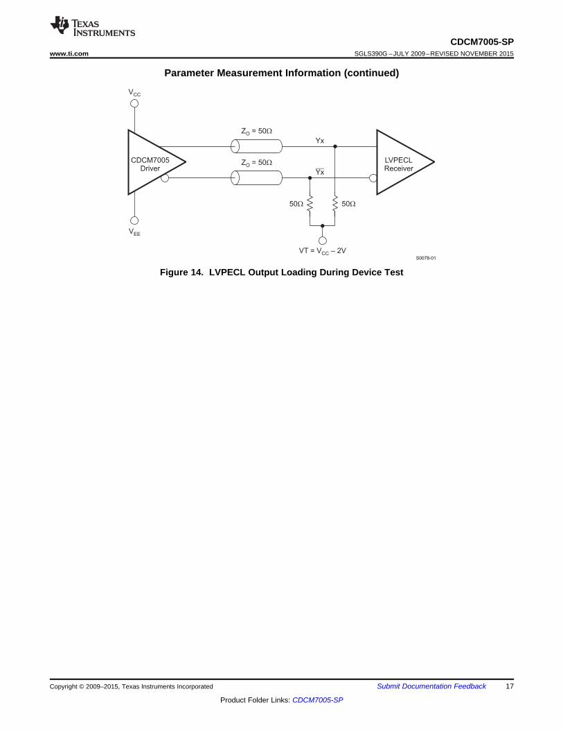
CDCM7005 VCXO LF VCXO IN VCXO IN CP OUT PRI REF YnA YnB OSC DAC Product Folder Sample & Buy Technical Documents Tools & Software Support & Community An IMPORTANT NOTICE at the end of this data sheet addresses availability, warranty, changes, use in safety-critical applications, intellectual property matters and other important disclaimers. PRODUCTION DATA. CDCM7005-SP SGLS390G – JULY 2009 – REVISED NOVEMBER 2015 CDCM7005-SP 3.3-V High Performance Rad-Tolerant Class V, Clock Synchronizer and Jitter Cleaner 1 1 Features 1• High Performance LVPECL and LVCMOS PLL Clock Synchronizer • Two Reference Clock Inputs (Primary and Secondary Clock) for Redundancy Support With Manual or Automatic Selection • Accepts LVCMOS Input Frequencies Up to 200 MHz • VCXO_IN Clock is Synchronized to One of the Two Reference Clocks • VCXO_IN Frequencies Up to 2 GHz (LVPECL) • Outputs can be a Combination of LVPECL and LVCMOS (Up to Five Differential LVPECL Outputs or Up to 10 LVCMOS Outputs) • Output Frequency is Selectable by x1, /2, /3, /4, /6, /8, /16 on Each Output Individually • Efficient Jitter Cleaning from Low PLL Loop Bandwidth • Low Phase Noise PLL Core • Programmable Phase Offset (PRI_REF and SEC_REF to Outputs) • Wide Charge Pump Current Range From 200 μA to 3 mA • Analog and Digital PLL Lock Indication • Provides VBB Bias Voltage Output for Single- Ended Input Signals (VCXO_IN) • Frequency Hold Over Mode Improves Fail-Safe Operation • Power-Up Control Forces LVPECL Outputs to Tri- State at V CC < 1.5 V • SPI Controllable Device Setting • 3.3-V Power Supply • High-Performance 52 Pin Ceramic Quad Flat Pack (HFG) • Rad-Tolerant : 50 kRad (Si) TID • QML-V Qualified, SMD 5962-07230 • Military Temperature Range: –55°C to 125°C T case • Engineering Evaluation (/EM) Samples are Available (1) These units are intended for engineering evaluation only. They are processed to a non-compliant flow (for example, no burn-in, and so forth) and are tested to temperature rating of 25°C only. These units are not suitable for qualification, production, radiation testing or flight use. Parts are not warranted for performance on full MIL specified temperature range of –55°C to 125°C or operating life. 2 Applications • Low-Jitter Clock Distribution • SERDES Links • Analog Data Converters • Digital-to-Analog Converters 3 Description The CDCM7005-SP is a high-performance, low phase noise and low skew clock synchronizer that synchronizes a VCXO (voltage controlled crystal oscillator) or VCO (voltage controlled oscillator) frequency to one of the two reference clocks. The programmable pre-divider M and the feedback- dividers N and P give a high flexibility to the frequency ratio of the reference clock to VC(X)O as VC(X)O_IN / PRI_REF = (N × P) / M or VC(X)O_IN / SEC_REF = (N × P) / M. VC(X)O_IN clock operates up to 2 GHz. Through the selection of external VC(X)O and loop filter components, the PLL loop bandwidth and damping factor can be adjust to meet different system requirements. Device Information (1) PART NUMBER PACKAGE BODY SIZE (NOM) CDCM7005-SP CFP (52) 13.97 mm × 13.97 mm (1) For all available packages, see the orderable addendum at the end of the data sheet. Typical Application Schematic
Transcript
CDCM7005
VCXO LF
VCXOIN
VCXOIN
CPOUT
PRIREF
YnA
YnB
OSC
DAC
Product
Folder
Sample &Buy
Technical
Documents
Tools &
Software
Support &Community
An IMPORTANT NOTICE at the end of this data sheet addresses availability, warranty, changes, use in safety-critical applications,intellectual property matters and other important disclaimers. PRODUCTION DATA.
CDCM7005-SPSGLS390G –JULY 2009–REVISED NOVEMBER 2015
CDCM7005-SP 3.3-V High Performance Rad-Tolerant Class V, Clock Synchronizer andJitter Cleaner
1
1 Features1• High Performance LVPECL and LVCMOS PLL
Clock Synchronizer• Two Reference Clock Inputs (Primary and
Secondary Clock) for Redundancy Support WithManual or Automatic Selection
• Accepts LVCMOS Input Frequencies Up to200 MHz
• VCXO_IN Clock is Synchronized to One of theTwo Reference Clocks
• VCXO_IN Frequencies Up to 2 GHz (LVPECL)• Outputs can be a Combination of LVPECL and
LVCMOS (Up to Five Differential LVPECL Outputsor Up to 10 LVCMOS Outputs)
• Output Frequency is Selectable by x1, /2, /3, /4,/6, /8, /16 on Each Output Individually
• Efficient Jitter Cleaning from Low PLL LoopBandwidth
(1) These units are intended for engineering evaluation only.They are processed to a non-compliant flow (for example, noburn-in, and so forth) and are tested to temperature rating of25°C only. These units are not suitable for qualification,production, radiation testing or flight use. Parts are notwarranted for performance on full MIL specified temperaturerange of –55°C to 125°C or operating life.
2 Applications• Low-Jitter Clock Distribution• SERDES Links• Analog Data Converters• Digital-to-Analog Converters
3 DescriptionThe CDCM7005-SP is a high-performance, lowphase noise and low skew clock synchronizer thatsynchronizes a VCXO (voltage controlled crystaloscillator) or VCO (voltage controlled oscillator)frequency to one of the two reference clocks. Theprogrammable pre-divider M and the feedback-dividers N and P give a high flexibility to thefrequency ratio of the reference clock to VC(X)O asVC(X)O_IN / PRI_REF = (N × P) / M or VC(X)O_IN /SEC_REF = (N × P) / M.
VC(X)O_IN clock operates up to 2 GHz. Through theselection of external VC(X)O and loop filtercomponents, the PLL loop bandwidth and dampingfactor can be adjust to meet different systemrequirements.
Device Information(1)
PART NUMBER PACKAGE BODY SIZE (NOM)CDCM7005-SP CFP (52) 13.97 mm × 13.97 mm
(1) For all available packages, see the orderable addendum atthe end of the data sheet.
13 Device and Documentation Support ................. 4513.1 Community Resources.......................................... 4513.2 Trademarks ........................................................... 4513.3 Electrostatic Discharge Caution............................ 4513.4 Glossary ................................................................ 45
14 Mechanical, Packaging, and OrderableInformation ........................................................... 45
4 Revision HistoryNOTE: Page numbers for previous revisions may differ from page numbers in the current version.
Changes from Revision F (January 2014) to Revision G Page
• Added ESD Ratings table, Feature Description section, Device Functional Modes, Application and Implementationsection, Power Supply Recommendations section, Layout section, Device and Documentation Support section, andMechanical, Packaging, and Orderable Information section ................................................................................................. 1
• Deleted two bullets from the Features List. ........................................................................................................................... 1
Changes from Revision E (August 2012) to Revision F Page
• Added /EM bullet to Features ................................................................................................................................................. 1• Deleted Ordering Information table ........................................................................................................................................ 4
Changes from Revision D (December 2011) to Revision E Page
• Changed PLL_LOCK pin description, replaced cycle-slip text. .............................................................................................. 5• Changed the Frequency Hold-Over Mode section ............................................................................................................... 24• Changed text From: Cycle-Slip To: Frequency Offset in Figure 22 ..................................................................................... 26• Changed table Word 3, Cycle Slip (Bit 6) To: Frequency Offset.......................................................................................... 32• Changed Note 1 of table Word 3.......................................................................................................................................... 32• Changed table Lock-Detect Window (Word 3) - Clip slip To: Frequency offset, and Note 2 ............................................... 34
Changes from Revision B (December 2009) to Revision C Page
• Changed the VCC pin text - From: There is no internal connection between VCC and AVCC To: VCC and AVCC shouldalways have same supply voltage.......................................................................................................................................... 5
• Added to the CTRL_LE - Unused or floating inputs must be tied to proper logic level. It is recommended to use a20-kΩ or larger pullup resistor to VCC ................................................................................................................................... 6
• Added to the CTRL_CLK pin - Unused or floating inputs must be tied to proper logic level. It is recommended to usea 20-kΩ or larger pullup resistor to VCC ................................................................................................................................ 6
• Added to the CTRL_DATA pin - Unused or floating inputs must be tied to proper logic level. It is recommended touse a 20-kΩ or larger pullup resistor to VCC ......................................................................................................................... 6
• Added to the PD pin text - It is recommended to ramp up the... ............................................................................................ 6• Added to the SPI CONTROL INTERFACE section - Unused or floating inputs must be tied to proper logic level. It is
recommended to use a 20-kΩ or larger pullup resistor to VCC ........................................................................................... 28• Added to the SPI CONTROL INTERFACE section - It is recommended to program Word 0, Word 1, Word 2 and
Word 3 right after power up and PD becomes HIGH........................................................................................................... 28• Changed bit 16 from RES to GTME..................................................................................................................................... 32• Changed bit 28 from RES to PFDFC ................................................................................................................................... 32
5 Description (continued)The CDCM7005-SP can lock to one of two reference clock inputs (PRI_REF and SEC_REF), supports frequencyhold-over mode and fast-frequency-locking for fail-safe and increased system redundancy. The outputs of theCDCM7005-SP are user definable and can be any combination of up to five LVPECL outputs or up to 10LVCMOS outputs. The LVCMOS outputs are arranged in pairs (Y0A:Y0B, Y1A:Y1B, …), so that each pair hasthe same frequency. But each output can be separately inverted and disabled. The built in synchronizationlatches ensure that all outputs are synchronized for low output skew.
All device settings, like outputs signaling, divider value, input selection, and many more, are programmable bySPI (3-wire serial peripheral interface). SPI allows individually control of the device settings.
The device operates in a 3.3-V environment and is characterized for operation from –55°C to 125°C (Tcase).
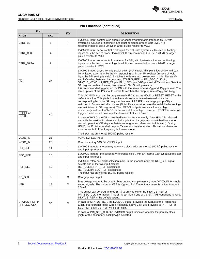
CTRL_LE 5 ILVCMOS input, control latch enable for serial programmable Interface (SPI), withhysteresis. Unused or floating inputs must be tied to proper logic level. It isrecommended to use a 20-kΩ or larger pullup resistor to VCC.
CTRL_CLK 4 ILVCMOS input, serial control clock input for SPI, with hysteresis. Unused or floatinginputs must be tied to proper logic level. It is recommended to use a 20-kΩ or largerpullup resistor to VCC.
CTRL_DATA 2 ILVCMOS input, serial control data input for SPI, with hysteresis. Unused or floatinginputs must be tied to proper logic level. It is recommended to use a 20-kΩ or largerpullup resistor to VCC.
PD 27 I
LVCMOS input, asynchronous power down (PD) signal. This pin is low active and canbe activated external or by the corresponding bit in the SPI register (in case of logichigh, the SPI setting is valid). Switches the device into power-down mode. Resets M-and N-Divider, 3-states charge pump, STATUS_REF, or PRI_SEC_CLK pin,STATUS_VCXO or I_REF_CP pin, PLL_LOCK pin, VBB pin and all Yx outputs. Sets theSPI register to default value; has internal 150-kΩ pullup resistor.It is recommended to ramp up the PD with the same time as VCC and AVCC or later. Theramp up rate of the PD should not be faster than the ramp up rate of VCC and AVCC.
RESET orHOLD 40 I
This LVCMOS input can be programmed (SPI) to act as HOLD or RESET. RESET is thedefault function. This pin is low active and can be activated external or via thecorresponding bit in the SPI register. In case of RESET, the charge pump (CP) isswitched to 3-state and all counters (N, M, P) are reset to zero (the initial divider settingsare maintained in SPI registers). The LVPECL outputs are static low and highrespectively and the LVCMOS outputs are all low or high if inverted. RESET is not edgetriggered and should have a pulse duration of at least 5 ns.In case of HOLD, the CP is switched in to 3-state mode only. After HOLD is releasedand with the next valid reference clock cycle the charge pump is switched back in tonormal operation (CP stays in 3-state as long as no reference clock is valid). DuringHOLD, the P divider and all outputs Yx are at normal operation. This mode allows anexternal control of the frequency hold-over mode.The input has an internal 150-kΩ pullup resistor.
VCXO_IN 21 I VCXO LVPECL inputVCXO_IN 20 I Complementary VCXO LVPECL input
PRI_REF 14 I LVCMOS input for the primary reference clock, with an internal 150-kΩ pullup resistorand input hysteresis.
SEC_REF 15 I LVCMOS input for the secondary reference clock, with an internal 150-kΩ pullup resistorand input hysteresis.
REF_SEL 12 I
LVCMOS reference clock selection input. In the manual mode the REF_SEL signalselects one of the two input clocks:REF_SEL [1]: PRI_REF is selected;REF_SEL [0]: SEC_REF is selected;The input has an internal 150-kΩ pullup resistor.
CP_OUT 8 O Charge pump output
VBB 18 OBias voltage output to be used to bias unused complementary input VCXO_IN for singleended signals. The output of VBB is VCC – 1.3 V. The output current is limited to about1.5 mA.
STATUS_REF orPRI_SEC_CLK 50 O
This output can be programmed (SPI) to provide either the STATUS_REF orPRI_SEC_CLK information. This pin is set high if one of the STATUS conditions is valid.STATUS_REF is the default setting.In case of STATUS_REF, the LVCMOS output provides the Status of the ReferenceClock. If a reference clock with a frequency above 2 MHz is provided to PRI_REF orSEC_REF STATUS_REF will be set high.In case of PRI_SEC_CLK, the LVCMOS output indicates whether the primary clock[high] or the secondary clock [low] is selected.
This LVCMOS output can be programmed (SPI) to provide either the STATUS_VCXOinformation or serve as current path for the charge pump (CP). STATUS_VCXO is thedefault setting.In case of STATUS_VCXO, the LVCMOS output provides the status of the VCXO input(frequencies above 2 MHz are interpreted as valid clock; active high).In case of I_REF_CP, it provides the current path for the external reference resistor(12 kΩ ±1%) to support an accurate charge pump current, optional. Do not use anycapacitor across this resistor to prevent noise coupling via this node. If the internal 12 kΩis selected (default setting), this pin can be left open.
PLL_LOCK 52 I/O
LVCMOS output for PLL_LOCK information. This pin is set high if the PLL is in lock (seefeature description). This output can be programmed to be digital lock detect or analoglock detect (see feature description).The PLL is locked (set high), if the rising edge either of PRI_REF or SEC_REF clockand VCXO_IN clock at the phase frequency detector (PFD) are inside the lock detectwindow for a predetermined number of successive clock cycles.The PLL is out-of-lock (set low), if the rising edge of either the PRI_REF or SEC_REF)clock and VCXO_IN clock at the PFD are outside the lock detect window or if a certainfrequency offset between reference frequency and feedback frequency (VCXO) isdetected.Both, the lock detect window and the number of successive clock cycles are userdefinable (via SPI).
Y0A:Y0BY1A:Y1BY2A:Y2BY3A:Y3BY4A:Y4B
24, 25,29, 30,33, 34,37,38,42, 43
OThe outputs of the CDCM7005-SP are user definable and can be any combination of upto five LVPECL outputs or up to 10 LVCMOS outputs. The outputs are selectable viaSPI (Word 1, Bit 2-6). The power-up setting is all outputs are LVPECL.
(1) Stresses beyond those listed under Absolute Maximum Ratings may cause permanent damage to the device. These are stress ratingsonly, which do not imply functional operation of the device at these or any other conditions beyond those indicated under RecommendedOperating Conditions. Exposure to absolute-maximum-rated conditions for extended periods may affect device reliability.
(2) All supply voltages have to be supplied at the same time.(3) The input and output negative voltage ratings may be exceeded if the input and output clamp-current ratings are observed.
7 Specifications
7.1 Absolute Maximum Ratingsover operating free-air temperature range (unless otherwise noted) (1)
MIN MAX UNITVCC,AVCC,VCC_CP
Supply voltage (2) –0.5 4.6 V
VI Input voltage (3) –0.5 V VCC + 0.5 V VVO Output voltage (3) –0.5 VCC + 0.5 V V
IOUTOutput current for LVPECL/LVCMOS outputs(0 < VO < VCC) ±50 mA
IIN Input current (VI < 0, VI > VCC) ±20 mATJ Maximum junction temperature 150 °CTstg Storage temperature –65 150 °C
(1) JEDEC document JEP155 states that 500-V HBM allows safe manufacturing with a standard ESD control process.(2) JEDEC document JEP157 states that 250-V CDM allows safe manufacturing with a standard ESD control process.
7.2 ESD RatingsVALUE UNIT
V(ESD)Electrostaticdischarge
Human body model (HBM), per ANSI/ESDA/JEDEC JS-001 (1) ±2500V
Charged-device model (CDM), per JEDEC specification JESD22-C101 (2) ±1500
(1) VIL and VIH are required to maintain ac specifications; the actual device function tolerates a smaller input level of 1V, if an ac-coupling toVCC/2 is provided.
(2) VINPP minimum and maximum is required to maintain ac specifications; the actual device function tolerates at a minimum VINPPof 150 mV.
7.3 Recommended Operating ConditionsMIN NOM MAX UNIT
VCC, AVCC Supply voltage3 3.3 3.6
VVCC_CP 2.3 VCC
VIL Low-level input voltage LVCMOS, see (1) 0.3 VCC VVIH High-level input voltage LVCMOS, see (1) 0.7 VCC VIOH High-level output current LVCMOS (includes all status pins) –8 mAIOL Low-level output current LVCMOS (includes all status pins) 8 mAVI Input voltage range LVCMOS 0 3.6 VVINPP Input amplitude LVPECL (VVCXO_IN – V VCXO_IN ) (2) 0.5 1.3 VVIC Common-mode input voltage LVPECL 1 VCC–0.3 VTC Operating case temperature –55 125 °C
(1) All typical values are at VCC = 3.3 V, temperature = 25°C.(2) ƒclk can be up to 400 MHz in the typical operating mode (25°C / 3.3-V VCC).(3) Operating the LVCMOS or LVPECL output above the maximum frequency will not cause a malfunction to the device, but the output
signal swing may no longer meet the output specification.(4) These inputs have an internal 150-kΩ pullup resistor.
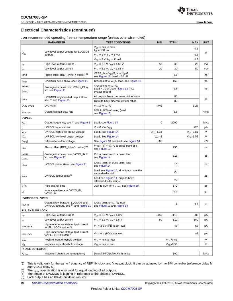
7.5 Electrical Characteristicsover recommended operating free-air temperature range (unless otherwise noted)
PARAMETER TEST CONDITIONS MIN TYP (1) MAX UNIT
OVERALL
ICC_LVPECL
Supply current (ICC over frequency seeFigure 2 through Figure 5)
Electrical Characteristics (continued)over recommended operating free-air temperature range (unless otherwise noted)
PARAMETER TEST CONDITIONS MIN TYP (1) MAX UNIT
(5) This is valid only for the same frequency of REF_IN clock and Y output clock. It can be adjusted by the SPI controller (reference delay Mand VCXO delay N).
(6) The tsk(o) specification is only valid for equal loading of all outputs.(7) The phase of LVCMOS is lagging in reference to the phase of LVPECL.(8) Lock output has an 80-kΩ pulldown resistor.
VOLLow-level output voltage for LVCMOSoutputs
VCC = min to max,IOL = 100 μA 0.1
VVCC = 3 V, IOL = 6 mA 0.5
VCC = 3 V, IOL = 12 mA 0.8
IOH High-level output current VCC = 3.3 V, VO = 1.65 V –50 –30 –20 mA
IOL Low-level output current VCC = 3.3 V, VO = 1.65 V 20 30 50 mA
tpho Phase offset (REF_IN to Y output) (5) VREF_IN = VCC/2, Y = VCC/2,see Figure 12, Load = 10 pF 2.7 ns
tsk(p) LVCMOS pulse skew, see Figure 11 Crosspoint to VCC/2 load, see Figure 13 160 ps
tpd(LH) Propagation delay from VCXO_IN toYx, see Figure 11
Crosspoint to VCC/2,Load = 10 pF, see Figure 13 (PLLbypass mode)
2.8 nstpd(HL)
tsk(o)LVCMOS single-ended output skew,see (6) and Figure 11
All outputs have the same divider ratio 80ps
Outputs have different divider ratios 80
Duty cycle LVCMOS VCC/2 to VCC/2 49% 51%
tslew-rate Output rise/fall slew rate 20% to 80% of swing (loadsee Figure 13) 3.5 V/ns
LVPECL
ƒclk Output frequency, see (3) and Figure 6 Load, see Figure 14 0 2000 MHz
II LVPECL input current VI = 0 V or VCC ±20 µA
VOH LVPECL high-level output voltage Load, See Figure 14 VCC–1.18 VCC–0.81 V
VOL LVPECL low-level output voltage Load, See Figure 14 VCC–2 VCC–1.55 V
|VOD| Differential output voltage See Figure 10 and load, see Figure 14 500 mV
tpho Phase offset (REF_IN to Y output) (6) VREF_IN = VCC/2 to cross point of Y,see Figure 12 250 ps
tpd(LH) Propagation delay time, VCXO_IN toYx, see Figure 11
Cross point-to-cross point, loadsee Figure 14 615 ps
tpd(HL)
tsk(p) LVPECL pulse skew, see Figure 11 Cross point-to-cross point, loadsee Figure 14 15 ps
tsk(o) LVPECL output skew (6)
Load see Figure 14, all outputs have thesame divider ratio 20
psLoad see Figure 14, outputs havedifferent divider ratios 50
tr / tf Rise and fall time 20% to 80% of VOUTPP, see Figure 10 170 ps
CIInput capacitance at VCXO_IN,VCXO_IN 2.5 pF
LVCMOS-TO-LVPECL
tsk(P_C)Output skew between LVCMOS andLVPECL outputs, see (7) and Figure 11
Cross point to VCC/2; load,see Figure 13 and Figure 14 2 3.2 ns
PLL ANALOG LOCK
IOH High-level output current VCC = 3.6 V, VO = 1.8 V –150 –110 –80 µA
IOL Low-level output current VCC = 3.6 V, VO = 1.8 V 80 110 150 µA
IOZH LOCKHigh-impedance state output currentfor PLL LOCK output (8) VO = 3.6 V (PD is set low) 45 65 µA
IOZL LOCKHigh-impedance state output currentfor PLL LOCK output (8) VO = 0 V (PD is set low) ±5 µA
VIT+ Positive input threshold voltage VCC = min to max VCC×0.55 V
VIT– Negative input threshold voltage VCC = min to max VCC×0.35 V
PHASE DETECTOR
ƒCPmax Maximum charge pump frequency Default PFD pulse width delay 100 MHz
ICPM Sink/source current matching 0.5 V < VCP < VCC_CP – 0.5 V, SPIdefault settings –7% 2.5% 7%
IVCPM ICP vs VCP matching 0.5 V < VCP < VCC_CP – 0.5 V –10% 5% 10%
(1) At Reference Clock less than 2 MHz, the device stays in normal operation mode but the frequency detection circuitry resets theSTATUS_REF signal to low. In this case, the status of the STATUS_REF is no longer relevant.
(2) ƒREF_IN can be up to 250 MHz in typical operating mode (25°C / 3.3-V VCC).(3) If the Feedback Clock (derives from VCXO input) is less than 2 MHz, the device stays in normal operation mode but the frequency
detection circuitry resets the STATUS_VCXO signal and PLL_LOCK signal to low. Both status signals are no longer relevant. Thiseffects the HOLD-over function as well, as the PLL_LOCK signal is no longer valid!
(4) Use a square wave for lower frequencies (<80 MHz).
7.6 Timing Requirementsover recommended ranges of supply voltage, load and operating free air temperature
MIN TYP MAX UNITPRI_REF/SEC_REF_IN REQUIREMENTSƒREF_IN LVCMOS primary or secondary reference clock frequency (1) (2) 0 200 MHztr/ tf Rise and fall time of PRI_REF or SEC_REF signals from 20% to 80% of VCC 4 nsdutyREF Duty cycle of PRI_REF or SEC_REF at VCC/2 40% 60%VCXO_IN, VCXO_IN REQUIREMENTSƒVCXO_IN VCXO clock frequency (3) 0 2000 MHztr/ tf Rise and fall time 20% to 80% of VINPP at 80 MHz to 800 MHz (4) 3 nsdutyVCXO Duty cycle of VCXO clock 40% 60%SPI/CONTROL REQUIREMENTS (see Figure 24)ƒCTRL_CLK CTRL_CLK frequency 20 MHztsu1 CTRL_DATA to CTRL_CLK setup time 10 nsth2 CTRL_DATA to CTRL_CLK hold time 10 nst3 CTRL_CLK high duration 25 nst4 CTRL_CLK low duration 25 nstsu5 CTRL_LE to CTRL_CLK setup time 10 nstsu6 CTRL_CLK to CTRL_LE setup time 10 nst7 CTRL_LE pulse width 20 nstr/ tf Rise and fall time of CTRL_DATA CTRL_CLK, CTRL_LE from 20% to 80% of VCC 4 nsPD, RESET, HOLD , REF_SEL REQUIREMENTStr / tf Rise and fall time of the PD, RESET, HOLD, REF_SEL signal from 20% to 80% of VCC 4 ns
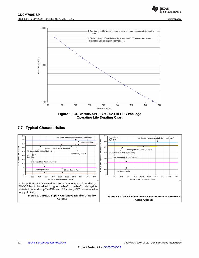
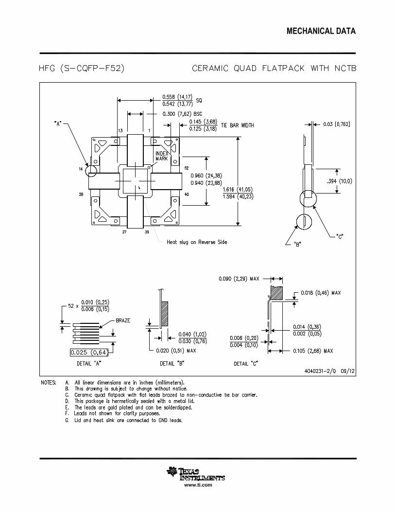
Figure 1. CDCM7005-SPHFG-V - 52-Pin HFG PackageOperating Life Derating Chart
7.7 Typical Characteristics
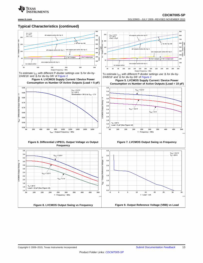
If div-by-2/4/8/16 is activated for one or more outputs, 'Δ for div-by-2/4/8/16' has to be added to ICC of div-by-1. If div-by-3 or div-by-6 isactivated, 'Δ for div-by-2/4/8/16' and 'Δ for div-by-3/6' has to be addedto ICC of div-by-1.
Figure 2. LVPECL Supply Current vs Number of ActiveOutputs
Figure 3. LVPECL Device Power Consumption vs Number ofActive Outputs
A. Output skew, tsk(o), is calculated as the greater of:The difference between the fastest and the slowest tpd(LH)n (n = 0...4)The difference between the fastest and the slowest tpd(HL)n (n = 0...4)
B. Pluse skew, tsk(p), is calculated as the magnitude of the absolute time difference between the high-to-low (tpd(HL)) andthe low-to-high (tpd(LH)) propagation delays when a single switching input causes one or more outputs to switch,tsk(p) = |tpd(HL) – tpd(LH) |. Pulse skew is sometimes refered to as pulse width distortion or duty cycle skew.
9.1 OverviewThe CDCM7005-SP is a high-performance, low phase noise and low skew clock synchronizer that synchronizesa VCXO or VCO frequency to one of the two reference clocks. VC(X)O_IN clock operates up to 2.0 GHz.Through the selection of external VC(X)O and loop filter components, the PLL loop bandwidth and dampingfactor can be adjust to meet different system requirements.
The CDCM7005-SP can lock to one of two reference clock inputs (PRI_REF and SEC_REF), supports frequencyhold-over mode and fast-frequency-locking for fail-safe and increased system redundancy. The outputs of theCDCM7005-SP are user definable and can be any combination of up to five LVPECL outputs or up to 10LVCMOS outputs. The LVCMOS outputs are arranged in pairs (Y0A:Y0B, Y1A:Y1B, …), so that each pair hasthe same frequency. But each output can be separately inverted and disabled. The built in synchronizationlatches ensure that all outputs are synchronized for low output skew.
CDCM7005-SP is programmable through SPI (3-wire serial peripheral interface). SPI allows individually controlof the device settings.
The device operates in a 3.3-V environment and is characterized for operation from –55°C to 125°C (Tcase).
9.3.1 Automatic/Manual Reference Clock SwitchingThe CDCM7005-SP supports two reference clock inputs, the primary clock input, PRI_REF, and the secondaryclock input, SEC_REF. The clocks can be selected manually or automatically. The respective mode is selectedby the dedicated SPI register bit (Word 0, Bit 30).
In the manual mode, the external REF_SEL signal selects one of the two input clocks:REF_SEL [1] -> primary clock is selectedREF_SEL [0] -> secondary clock is selected
In the automatic mode, the primary clock is selected by default even if both clocks are available. In case theprimary clock is not available or fails, then the input switches to the secondary clock as long until the primaryclock is back. Figure 15 shows the automatic clock selection.
NOTE: PRI_REF is the preferred clock input.
Figure 15. Behavior of STATUS_REF and PRI_SEC_CLK
In the automatic mode, the frequencies of both clock signals have to be similar, but may differ by up to 20%. Thephase of the clock signal can be any.
The clock input circuitry is design to suppress glitches during switching between the primary and secondary clockin the manual and automatic mode. This avoids an undefined switching of the following circuitries.
The phase of the output clock slowly follows the new input phase. There will be no phase jump at the output.How quick the phase adjustment is done depends on the selected loop parameter, i.e., at a loop bandwidth of<100 Hz; the phase adjustment can take several ms. There is no phase build-out function supported (like inSONET/SDH applications).
Figure 16. Phase Approach of Output to New Reference Clock
9.3.2 PLL Lock for Analog and Digital DetectThe CDCM7005-SP supports two PLL lock indications: the digital lock signal or the analog lock signal. Bothsignals indicate logic high-level at PLL_LOCK if the PLL locks according the selected lock condition.
9.3.2.1 PLL Lock/Out-of-Lock DefinitionThe PLL is locked (set high), if the rising edge of the Reference Clock (PRI_REF or SEC_REF clock) andFeedback Clock (VCXO_IN clock) at the PFD (phase frequency detect) are inside a predefined lock detectwindow, or if no cycle-slip appears, for a pre-defined number of successive clock cycles.
The PLL is out-of-lock (set low), if the rising edge of the Reference Clock (PRI_REF or SEC_REF clock) andFeedback Clock (VCXO_IN clock) at the PFD are outside the predefined lock detect window or if a cycle-slipappears.
Both, the lock detect window and the number of successive clock cycles are user definable (Word 3, Bit 2-6).
Figure 17. Lock Detect Window
The lock detect window describes the maximum allowed time difference for lock detect between the rising edgeof PRI_REF or SEC_REF and VCXO_IN. The time difference is detected at the phase frequency detector. Therising edge of PRI_REF or SEC_REF is taken as reference. The rising edge of VCXO_IN is outside the lockdetect window if there is a phase displacement of more than +0.5 × t(lockdetect) or –0.5 × t(lockdetect).
Feature Description (continued)9.3.2.2 Digital vs Analog LockFigure 18 and Figure 19 show the circuit for the digital and analog lock. The analog lock operates with anexternal load capacitor.
When selecting the digital PLL lock option, PLL_LOCK will possibly jitter several times between lock and out oflock until a stable lock is detected. A single low-to-high step can be reached with a wide lock detect window andhigh number of successive clock cycles. PLL_LOCK returns to out of lock if just one cycle is outside the lockdetect window or a cycle slip occurs.
Figure 18. Digital Lock-Detect
When selecting the analog PLL Lock option, the high-pulses load the external capacitor via the internal 110-µAcurrent source until logic high-level is reached. Therefore, more time is needed to detect logic high level, butjittering of PLL_LOCK will be suppressed in case of digital lock. The time PLL_LOCK needs to return to out oflock depends on the level of VOut, when the current source starts to unload the external capacitor.
Feature Description (continued)9.3.3 Differential LVPECL Outputs and Single-Ended LVCMOS OutputsThe CDCM7005-SP supports up to 5 × LVPECL outputs or 10 × LVCMOS/LVTTL outputs or any combination ofthese. The single ended LVCMOS outputs are arranged in pairs which mean both outputs of a LVCMOS pairhave the same frequency but can separately be disabled or inverted. The power up output arrangement is fiveLVPECL (default setting).
The LVPECL outputs are designed to terminate in to a 50-Ω load to VCC – 2 V. The LVCMOS outputs supportsthe standard LVCMOS load (see Figure 13). The LVPECL and LVCMOS outputs can be enabled (normaloperation) or disabled (3-state).
In addition, the output phase can be shifted by 90 degrees when using the additional div-by-4 or div-by-8 modeof the P16-Div (see Figure 20). In the default mode (after power up), the div-by-16 mode of the P16-Div is active.To change it to a 90 degree phase shift, bit 30 or bit 31 of word 1 has to be programmed accordingly. The P 16-Div has to be selected via the dedicated YxMUX to obtain the 90 degree phase shift. The outputs are switched inpairs. When selecting the 90 degree phase shift mode, the div-by-16 functions will no longer be available. The 90degree phase shifted signal is lagging to the non-shifted signal.
Figure 20. 90 Degree Phase Shift Option of P-Divider
Figure 21 shows the LVCMOS and LVPECL output signal when 90 degree phase shift is on.
In addition, the LVCMOS supports disabled-to-low and 180° output phase shift for each output individually. Whenselecting the 180° phase shift together with the 90° phase shift, the respective outputs has a total phase shift of270° (see Table 1).
0° Any P-Divider No div-by-1690° P16-Div No div-by-4 or div-by-8180° Any P-Divider Yes div-by-16270° P16-Div Yes div-by-4 or div-by-8
If the P16-Div is selected by the FB_MUX and div-by-4 or div-by-8 is active, the 90° phase shifted clock will besynchronized to PRI_REF or SEC_REF. This means all outputs Yxx, which are switched to div-by-4 or div-by-8,are in phase to PRI_REF or SEC_REF. All other outputs are 90° phase shifted with leading phase.
9.3.4 Frequency Hold-Over ModeThe HOLD function is a useful feature which helps the designer to improve the system reliability. The HOLDfunction holds the output frequency in case the input reference clock fails or becomes disrupted. During HOLD,the charge pump switches off (3-state) freezing the last valid output frequency. The hold function will releaseafter a valid reference clock comes back. For proper HOLD function, the analog PLL lock detect mode has to beactive.
The following register settings are involved with the HOLD function:• Lock Detect Window (Word 3, Bit 2, 3, 6): Defines the window in ns inside the lock is valid. The size is
3.5 ns, 8.5 ns, 18.5 ns, or a certain frequency offset. Lock sets if reference clock and the feedback clock areinside this predefined lock-detect window for a pre-selected number of successive cycles or if no frequencyoffset appears.
• Out-of-Lock: Defines the out-of-lock condition: If the reference clock and the feedback clock at the PFD areoutside the predefined Lock Detect Window or if a certain frequency offset occurs.
• Cycle-Slip (Word 3, Bit 6): A Frequency offset occurs if a certain frequency offset between referencefrequency and feedback frequency (VCXO) at PFD input is detected. The minimum detectable frequencyoffset depends on the device setting and can be calculated:
where• foffsetPFD = detectable frequency offset at PFD between the reference frequency (fREF) and feedback frequency
(fFB)• fPFD = frequency at phase-frequency detection circuitry• PWD = PFD Pulse Width Delay (1)
• Number of Clock Cycles (Word 3, Bit 4, 5): Defines the number of successive PFD cycles which have tooccur inside the lock window to set Lock detect. This applies not for out-of-lock condition.
• Hold-Function (Word 3, Bit 9): Selects HOLD function (see more details below).• Hold-Trigger (Word 3, Bit 11): Defines whether the HOLD function is always activated (Bit 11 = [1]) or whether
it is dependent on the state of the analog PLL lock detect output (Bit 11 = [0]). In the latter case, HOLD isactivated, if lock is set (high) and de-activated if Lock is reset (low).
• Analog PLL Lock Detect (Word 1, Bit 29): Analog lock output charges or discharges an external capacitor withevery valid lock cycle. The time constant for Lock detect can be set by the value of the capacitor.
The CDCM7005 supports two types of HOLD functions, one external controllable HOLD mode and one internalmode, HOLD.
With the external HOLD function the charge pump can directly be switched into 3-state (pin H8 [BGA] or pin 14[QFN] can be programmed for HOLD [Word 2, Bit 29]). This function is also available via SPI register (Word 2,Bit 31).
If logic low is applied to the HOLD pin, the charge pump will be switched to 3-state. After the HOLD pin isreleased, the charge pump is switched back in to normal operation with the next valid reference clock cycle atPRI_REF or SEC_REF and the next valid feedback clock cycle at the PFD. During HOLD, the P divider and alloutputs Yx are at normal operation.
HOLD-Over-Function: The PLL has to be in lock to start the HOLD function. It switches the charge pump in to 3-State when an out-of-lock event occurs. It leaves the 3-state charge pump state when the reference clock isback. Then it starts a locking sequence of 64 cycles before it goes back to the beginning of the HOLD-over loop.The dedicated looking sequence and a digital phase alignment enable a fast lock.
9.3.5 Charge Pump Preset to VCC_CP / 2The preset charge pump to VCC_CP/2 is a useful feature to quickly set the center frequency of the VC(X)O afterpowerup or reset. The adequate control voltage for the VC(X)O will be provided to the charge-pump output by aninternal voltage divider of 1 kΩ/1 kΩ to VCC_CP and GND (VCC_CP/2).
This feature helps to get the initial frequency accuracy, i.e. required at common public radio interface (CPRI) oropen base station architecture initiative (OBSAI).
The preset charge pump to VCC_CP/2 can be set and reset by SPI register (word 2, bit 3). This feature must bedisabled for PLL locking.
9.3.6 Charge Pump Current DirectionThe direction of the charge pump (CP) current pulse can be changed by the SPI register (word 2, bit 2). Itdetermines in which direction the CP current regulates (reference clock leads to feedback clock). Mostapplications use the positive CP output current (power-up condition) because of the use of a passive loop filter.The negative CP current is useful when using an active loop filter concept with inverting operational amplifier.Figure 23 shows the internal PFD signal and the corresponding CP current.
NOTE: The purpose of the PFD pluse width delay is to improve spurious suppression.
Figure 23. Charge Pump Current Direction (VCXO and VCO Support)
9.4 Device Functional ModesDevice starts up in normal operational mode and might enter RESET or power-down modes by external signal orby writing to internal SPI registers.
CDCM7005-SP enters the power-down mode if PD signal is activated (LOW) or by writing to the correspondingbit in the configuration registers R02[28]. this power-down mode resets M- and N-Divider, tri-states charge pump,STATUS_REF, or PRI_SEC_CLK pin, STATUS_VCXO or I_REF_CP pin, PLL_LOCK pin, VBB pin and all Yxoutputs. This mode resets all the SPI registers to the default value. In this mode maximum current consumptionis 300 µA.
CDCM7005-SP enters the RESET mode when RESET pin is activated (LOW), given that this pin is configured asRESET by R02[29], or by writing to the corresponding bit R02[30]. In case of RESET, the charge pump (CP) isswitched to 3-state and all counters (N, M, P) are reset to zero (the initial divider settings are maintained in SPIregisters). The LVPECL outputs are static low and high respectively and the LVCMOS outputs are all low or highif inverted. Note that RESET is not edge triggered and should have a pulse duration of at least 5 ns.
9.5.1 SPI Control InterfaceThe serial interface of the CDCM7005-SP is a simple SPI-compatible interface for writing to the registers of thedevice and consists of three control lines: CTRL_CLK, CTRL_DATA, and CTRL_LE. There are four 32 bit wideregisters, which can be addressed by the two LSBs of a transferred word (bit 0 and bit 1). Every transmitted wordmust have 32 bits, starting with MSB first. Each word can be written separately. Bit 7, 8, 10, and Bit 12 to 31 ofWord 3 are reserved for factory test purposes and must be filled with zeros. The transfer is initiated with thefalling edge of CTRL_LE; as long as CTRL_LE is high, no data can be transferred. During CTRL_LE, low datacan be written. The data has to be applied at CTRL_DATA and has to be stable before the rising edge ofCTRL_CLK. The transmission is finished by a rising edge of CTRL_LE. With the rising edge of CTRL_LE, thenew word is asynchronously transferred to the internal register (for example, N, M, P, ...). Each word has to beseparately transmitted by this procedure. Unused or floating inputs must be tied to proper logic level. It isrecommended to use a 20-kΩ or larger pullup resistor to VCC.
Figure 24. Timing Diagram SPI Control Interface
The SPI serial protocol accepts word Write operation only. There is neither a read, acknowledge, nor ahandshake operation.
The following four words include the register settings of the programmable functions of the CDCM7005-SP. It canbe modified to the customer application by changing one or more bits. It comes up with a default register settingafter power up or if the power down (PD) control signal is applied. The default setting is shown in column five ofthe following words.
It is recommended to program Word 0, Word 1, Word 2 and Word 3 right after power up and PD becomes HIGH.
A low active function is shown as [0] and a high active function is shown as [1].
(1) The frequency applied to the Divider N must be smaller than 250 MHz. A sufficient P Divider must be selected with the FB_MUX tomaintain this criteria.
(2) If set to low, STATUS_REF will be in normal operation. If set to high, STATUS_REF will be high, even if no valid clock isdetected (<2 MHz). This is useful for reference inputs frequencies less than 2 MHz where the frequency detection circuitry normallyresets the STATUS_REF signal to low.
Table 2. Word 0
BIT BIT NAME DESCRIPTION/FUNCTION POWER UPCONDITION PINS AFFECTED
0 C0 Register Selection 01 C1 Register Selection 02 M0 Reference Divider M Reference Divider M Bit 0 13 M1 Reference Divider M Bit 1 14 M2 Reference Divider M Bit 2 15 M3 Reference Divider M Bit 3 16 M4 Reference Divider M Bit 4 17 M5 Reference Divider M Bit 5 18 M6 Reference Divider M Bit 6 19 M7 Reference Divider M Bit 7 010 M8 Reference Divider M Bit 8 011 M9 Reference Divider M Bit 9 012 N0 VC(X)O Divider N (1) VCXO Divider N Bit 0 113 N1 VCXO Divider N Bit 1 114 N2 VCXO Divider N Bit 2 115 N3 VCXO Divider N Bit 3 116 N4 VCXO Divider N Bit 4 117 N5 VCXO Divider N Bit 5 118 N6 VCXO Divider N Bit 6 119 N7 VCXO Divider N Bit 7 020 N8 VCXO Divider N Bit 8 021 N9 VCXO Divider N Bit 9 022 N10 VCXO Divider N Bit 10 023 N11 VCXO Divider N Bit 11 024 DLYM0 Progr. Delay M Reference Phase Delay M Bit 0 025 DLYM1 Reference Phase Delay M Bit 1 026 DLYM2 Reference Phase Delay M Bit 2 027 DLYN0 Progr. Delay N Feedback Phase Delay N Bit 0 028 DLYN1 Feedback Phase Delay N Bit 1 029 DLYN2 Feedback Phase Delay N Bit 2 030 MANAUT Manual or Auto Ref. Manual Reference Clock Selection [0]
Automatic Reference Clock Selection [1]0 14, 15
31 REFDEC Freq. Detect Reference Frequency Detection on [0],off [1] (2)
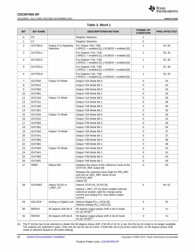
(1) The P 16-Div has to be selected to obtain the 90 degree phase shift. If bit 30 or bit 31 is set, the Div-by-16 mode is no longer available.The outputs are switched in pairs. Only one bit can be set at a time. If both bits set to [1] at the same time, no 90 degree phase shiftmode is selected (equal to off-mode setting).
Table 3. Word 1
BIT BIT NAME DESCRIPTION/FUNCTION POWER UPCONDITION PINS AFFECTED
7 OUT0A0 Output Y0 Mode Output Y0A Mode Bit 0 0 248 OUT0A1 Output Y0A Mode Bit 1 0 249 OUT0B0 Output Y0B Mode Bit 0 0 2510 OUT0B1 Output Y0B Mode Bit 1 0 2511 OUT1A0 Output Y1 Mode Output Y1A Mode Bit 0 0 2912 OUT1A1 Output Y1A Mode Bit 1 0 2913 OUT1B0 Output Y1B Mode Bit 0 0 3014 OUT1B1 Output Y1B Mode Bit 1 0 3015 OUT2A0 Output Y2 Mode Output Y2A Mode Bit 0 0 3316 OUT2A1 Output Y2A Mode Bit 1 0 3317 OUT2B0 Output Y2B Mode Bit 0 0 3418 OUT2B1 Output Y2B Mode Bit 1 0 3419 OUT3A0 Output Y3 Mode Output Y3A Mode Bit 0 0 3720 OUT3A1 Output Y3A Mode Bit 1 0 3721 OUT3B0 Output Y3B Mode Bit 0 0 3822 OUT3B1 Output Y3B Mode Bit 1 0 3823 OUT4A0 Output Y4 Mode Output Y4A Mode Bit 0 0 4224 OUT4A1 Output Y4A Mode Bit 1 0 4225 OUT4B0 Output Y4B Mode Bit 0 0 4326 OUT4B1 Output Y4B Mode Bit 1 0 4327 SREF Status Ref. Displays the status of the reference clock at the
STATUS_REF output [0]0 50
Displays the selected clock (high for PRI_REFand low for SEC_REF clock) at theSTATUS_REFoutput [1]
28 SXOIREF Status VCXO orI_REF_CP
Selects STATUS_VCXO [0] 0 49, 52Selects I_REF_CP [1] which enable externalreference resistor used for charge pumpcurrent and analog PLL lock detect outputcurrent.
29 ADLOCK Analog or Digital Lock Selects Digital PLL_LOCK [0]Selects Analog PLL_LOCK [1]
0 52
30 90DIV4 90 degree shift div-4 90 degree output phase shift in div-4 modeon [1]; off [0] (1)
0 Yx
31 90DIV8 90 degree shift div-8 90 degree output phase shift in div-8 modeon [1]; off [0] (1)
AFFECTED0 C0 Register Selection 01 C1 Register Selection 12 CP_DIR CP Direction Determines in which direction CP current regulates (Reference
Clock leads to Feedback Clock – see Figure 23)0 8
– positive CP output current [0];– negative CP output current [1];
3 PRECP Preset charge pump output voltage to VCC_CP/2, on [1], off [0] 0 84 CP0 CP Current CP Current Setting Bit 0 0 85 CP1 CP Current Setting Bit 1 1 86 CP2 CP Current Setting Bit 2 0 87 CP3 CP Current Setting Bit 3 1 88 PFD0 PFD Pulse
WidthPFD Pulse Width PFD Bit 0 0 8
9 PFD1 PFD Pulse Width PFD Bit 1 0 810 FBMUX0 FB_MUX Feedback MUX Select Bit 0 111 FBMUX1 Feedback MUX Select Bit 1 012 FBMUX2 Feedback MUX Select Bit 2 113 Y0MUX0 Y0_MUX Output Y0x Select Bit 0 1 24, 2514 Y0MUX1 Output Y0x Select Bit 1 0 24, 2515 Y0MUX2 Output Y0x Select Bit 2 1 24, 2516 Y1MUX0 Y1_MUX Output Y1x Select Bit 0 1 29, 3017 Y1MUX1 Output Y1x Select Bit 1 0 29,3018 Y1MUX2 Output Y1x Select Bit 2 1 29,2019 Y2MUX0 Y2_MUX Output Y2x Select Bit 0 1 33, 3420 Y2MUX1 Output Y2x Select Bit 1 0 33, 3421 Y2MUX2 Output Y2x Select Bit 2 1 33, 3422 Y3MUX0 Y3_MUX Output Y3x Select Bit 0 1 37, 3823 Y3MUX1 Output Y3x Select Bit 1 0 37, 3824 Y3MUX2 Output Y3x Select Bit 2 1 37, 3825 Y4MUX0 Y4_MUX Output Y4x Select Bit 0 1 42, 4326 Y4MUX1 Output Y4x Select Bit 1 0 42, 4327 Y4MUX2 Output Y4x Select Bit 2 1 42, 4328 PD Power Down mode on [0], off [1] 1 Yx29 RESHOL RESET or HOLD Pin definition: RESET [0] or HOLD [1] 0 4030 RESET Resets all dividers [0] - (equal to RESET pin function) 131 HOLD 3-state charge pump [0] - (equal to HOLD pin function) 1 8
(1) If Frequency offset mode only for out-of-lock detection is on, the selected lock detect window is valid for lock detect. Independent fromthis, out of lock is valid if a frequency offset is detected.
(2) HOLD function always activated is recommended for test purposes only.(3) The maximum frequency for the STATUS_VCXO pin is 100 MHz.
Table 5. Word 3
BIT BITNAME DESCRIPTION/FUNCTION POWER UP
CONDITIONPINS
AFFECTED0 Register selection 11 Register selection 12 LOCKW 0 Lock Window Lock-detect window Bit 0 1 523 LOCKW 1 Lock-detect window Bit 1 0 524 LOCKC0 Lock Cycles Number of coherent lock events Bit 0 0 525 LOCKC1 Number of coherent lock events Bit 1 1 526 FOFF Frequency Offset Frequency offset mode only for out-of-lock detection on
[1] or off [0] (1)0 52
7 RES RESERVED 0 RES8 RES RESERVED 0 RES9 HOLDF HOLD Function Enables the frequency hold-over function on [1], off [0] 010 RESERVED 0 RES11 HOLDTR HOLD Trigger
ConditionHOLD function always activated [1]; (2)
Triggered by analog PLL lock detect outputs [0] (ifanalog PLL Lock signal is set then HOLD is activated; ifanalog PLL lock signal is reset then HOLD is de-activated).
0
12 RES RESERVED 0 RES13 RES RESERVED 0 RES14 RES RESERVED 0 RES15 RES RESERVED 0 RES16 GTME General Test Mode Enable. Test Mode is only enabled if
this bit is set to 1.0
17 RES RESERVED 0 RES18 RES RESERVED 0 RES19 RES RESERVED 0 RES20 RES RESERVED 0 RES21 RES RESERVED 0 RES22 RES RESERVED 0 RES23 RES RESERVED 0 RES24 RES RESERVED 0 RES25 RES RESERVED 0 RES26 RES RESERVED 0 RES27 RES RESERVED 0 RES28 PFDFC PFD Frequency Control. Data provided to the PFD are
feed through to the corresponding STATUS pins. (3)0 49
29 RES RESERVED 0 RES30 RES RESERVED 0 RES31 RES RESERVED 0 RES
(1) If the divider value is Q, then the code will be the binary value of (Q–1).(2) The frequency applied to the Divider N must be smaller than 250 MHz. A sufficient P Divider must be selected with the FB_MUX to
maintain this criteria.
Table 7. VC(X)O Feedback Divider N (Word 0) (1) (2)
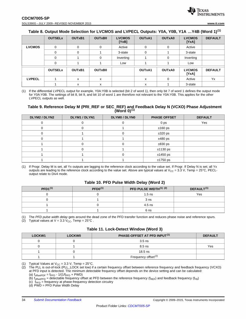
(1) If the differential LVPECL output for example, Y0A:Y0B is selected (bit 2 of word 1), then only bit 7 of word 1 defines the output modefor Y0A:Y0B. The settings of bit 8, bit 9, and bit 10 of word 1 are therefore not relevant to the Y0A:Y0B. This applies for the otherLVPECL outputs as well.
Table 8. Output Mode Selection for LVCMOS and LVPECL Outputs: Y0A, Y0B, Y1A …Y4B (Word 1) (1)
(1) If Progr. Delay M is set, all Yx outputs are lagging to the reference clock according to the value set. If Progr. If Delay N is set; all Yxoutputs are leading to the reference clock according to the value set. Above are typical values at VCC = 3.3 V, Temp = 25°C, PECL-output relate to Div4 mode.
Table 9. Reference Delay M (PRI_REF or SEC_REF) and Feedback Delay N (VCXO) Phase Adjustment(Word 0) (1)
(1) The PFD pulse width delay gets around the dead zone of the PFD transfer function and reduces phase noise and reference spurs.(2) Typical values at V = 3.3 VCC, Temp = 25°C .
(1) Typical Values at VCC = 3.3 V, Temp = 25°C.(2) The PLL is out-of-lock (PLL_LOCK set low) if a certain frequency offset between reference frequency and feedback frequency (VCXO)
at PFD input is detected. The minimum detectable frequency offset depends on the device setting and can be calculated:(a) foffsetPDF = fPFD - 1/(1/fPFD + PWD)(b) foffsetPFD = detectable frequency offset at PFD between the reference frequency (fREF) and feedback frequency (fFB)(c) fPFD = frequency at phase-frequency detection circuitry(d) PWD = PFD Pulse Width Delay
(1) This divider setting depends on the selected P-divider mode for the “Div-by-16” divider. In the default mode (after power up), Div-by-16is selected. But if bit 30 or bit 31 of word 1 is set to [1], then the Div-by-4 and 90 degree phase shift or Div-by-8 and 90 degree phaseshift is selected.
Table 14. FB_MUX Selection (Word 2)FBMUX2 FBMUX1 FBMUX0 SELECTED VC(X)O SIGNAL FOR THE PHASE
DISCRIMINATORDEFAULT
0 0 0 Div by 10 0 1 Div by 20 1 0 Div by 30 1 1 Div by 41 0 0 Div by 61 0 1 Div by 8 Yes1 1 0 Div by 16 (1)
1 1 1 Div by 8
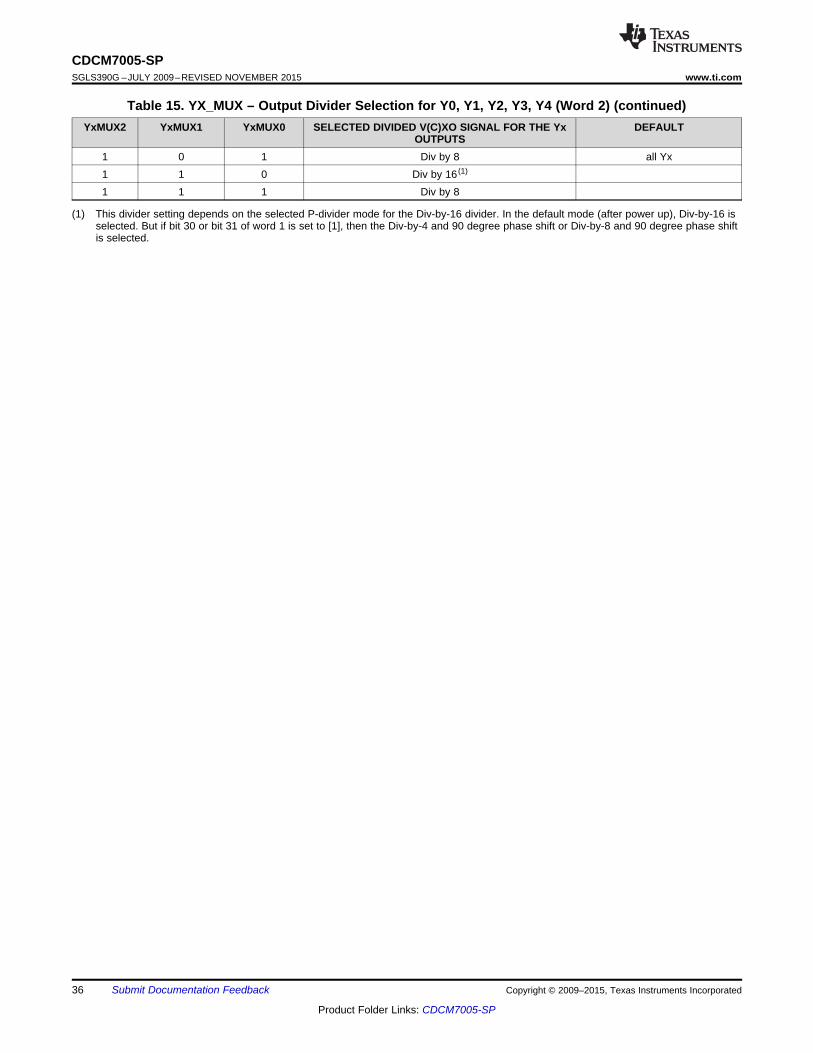
Table 15. YX_MUX – Output Divider Selection for Y0, Y1, Y2, Y3, Y4 (Word 2)YxMUX2 YxMUX1 YxMUX0 SELECTED DIVIDED V(C)XO SIGNAL FOR THE Yx
OUTPUTSDEFAULT
0 0 0 Div by 10 0 1 Div by 20 1 0 Div by 30 1 1 Div by 41 0 0 Div by 6
Table 15. YX_MUX – Output Divider Selection for Y0, Y1, Y2, Y3, Y4 (Word 2) (continued)YxMUX2 YxMUX1 YxMUX0 SELECTED DIVIDED V(C)XO SIGNAL FOR THE Yx
OUTPUTSDEFAULT
(1) This divider setting depends on the selected P-divider mode for the Div-by-16 divider. In the default mode (after power up), Div-by-16 isselected. But if bit 30 or bit 31 of word 1 is set to [1], then the Div-by-4 and 90 degree phase shift or Div-by-8 and 90 degree phase shiftis selected.
NOTEInformation in the following applications sections is not part of the TI componentspecification, and TI does not warrant its accuracy or completeness. TI’s customers areresponsible for determining suitability of components for their purposes. Customers shouldvalidate and test their design implementation to confirm system functionality.
10.1 Application Information
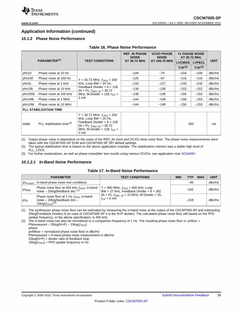
10.1.1 Clock Generation for Interpolating DACs With the CDCM7005-SPThe CDCM7005-SP, with its specified phase noise performance, is an ideal sampling clock generator for highspeed ADCs and DACs. The CDCM7005-SP is especially of interest for the new high speed DACs, which haveintegrated interpolation filter. Such DACs achieve sampling rates up to 500 MSPS. This high data rate cantypically not be supported from the digital side driving the DAC (for example, DUC, digital up-converter).Therefore, one approach to interface the DUC to the DAC is the integration of an interpolation filter within theDAC to reduce the data rate at the digital input of the DAC. In 3G systems, for example, a common samplingrate of a high speed DAC is 491.52 MSPS. With a four times interpolation of the digital data, the required inputdata rate results into 122.88 MSPS, which can be supported easily from the digital side. The DUC GC5016,which supports up to four WCDMA carriers, provides a maximum output data rate of 150 MSPS. An example isshown in Figure 25, where the CDCM7005-SP supplies the clock signal for the DUC/DDC and ADC/DAC.
Figure 25. CDCM7005-SP as a Clock Generator for High Speed ADCs and DACs
The generation of the two required clock signals (data input clock, clock for DAC) for such an interpolating DACcan be done in different ways. The recommended way is to use the CDCM7005-SP, which generates the fastsampling clock for the DAC from the data input clock signal. The DAC5687 demands that the edges of the twoinput clocks must be phase aligned within ±500 ps for latching the data properly. This phase alignment is wellachieved with the CDCM7005-SP, which assures a maximum skew of 70 ps of the different outputs to eachother.
Application Information (continued)10.1.1.1 AC-Coupled Interface to ADC/DACAnother advantage of this clock solution is that the ADC or DAC can be driven directly in an ac-coupling interfaceas shown in Figure 26, with an external termination in a differential configuration. There is no need for atransformer to generate a differential signal from a single-ended clock source.
Figure 26. Driving DAC or ADC With PECL Output of the CDCM7005-SP
(1) Output phase noise is dependent on the noise of the REF_IN clock and VCXO clock noise floor. The phase noise measurements weretaken with the CDCM7005-SP EVM and CDCM7005-SP SPI default settings.
(2) The typical stabilization time is based on the above application example. The stabilization criterion was a stable high level ofPLL_LOCK.
(3) For further explanations, as well as phase noise/jitter test results using various VCXOs, see application note SCAA067.
(1) The synthesizer phase noise floor can be estimated by measuring the in-band noise at the output of the CDCM7005-SP and subtracting20log(Feedback Divider) N (in case of CDCM7005-SP it is the N+P divider). The calculated phase noise floor still based on the PFDupdate frequency, in the above specification, is 400 kHz.
(2) The in-band noise can also be normalized to a comparison frequency of 1 Hz. The resulting phase noise floor is: pnfloor =PNmeasured – 20log(N+P) – 10log(ƒPFD)where:pnNfloor = normalized phase noise floor in dBc/HzPNmeasured = in-band phase noise measurement in dBc/Hz20log(N+P) = divider ratio of feedback loop10log(ƒPFD) = PFD update frequency in Hz
10.1.2.1 In-Band Noise Performance
Table 17. In-Band Noise PerformancePARAMETER TEST CONDITIONS MIN TYP MAX UNIT
Figure 27. Typical Application Diagram With Passive Loop Filter
10.2.1 Design RequirementsBefore PLL design starts, design targets and constraints should be specified.
Design targets include: output frequency, output phase noise or output jitter over certain band, maximum locktime or maximum dynamic frequency deviation during settling.
Design constraints might include: input frequency, specific VCO/VCXO device, certain type of filter (for example,passive)
Most probably VCO/VCXO is determined based on the noise requirements, or frequency plan needs. Inputfrequency is typically given by application or system needs. Power or noise requirement might dictate certaintype of filter.
Typical Application (continued)10.2.2 Detailed Design ProcedureThe CDCM7005-SP design procedure aims at:• Properly configuring the PLL dividers to achieve lock under given frequency plan• Determining loop BW/phase margin/gain peaking to achieve given noise/dynamic performance• Determine the filter type and component values based on the loop BW/phase margin
The proper division ratios can be calculated from the given relations:• fout: The desired output frequency (240 MHz for LVCMOS, 1.5 GHz max for LVPECL)• fin: The given input frequency (200 MHz maximum)• fVCO : The selected VCO or VCXO frequency (2.0 GHz maximum)• fPFD: The update frequency of the PFD, 100 MHz maximum• M : Reference divider (10 bits: 1 to 1024)• P2 : Output divider, also known as Output Mux (/1, /2, /3, /4, /6, /8, /16)• P1 : Pre-scalar, also known as Feedback Mux (/1, /2, /3, /4, /6, /8, /16)• N : Feedback divider (12 bits: 1 to 4096), with max input freq of 300 MHz.
Once frequency plan and feasible divider settings are determined, a proper BW/phase margin and gain peakingshould be determined. The best way to determine those parameters is to use the TI CDCM7005-SP PLLCalculator tool (PLL-SIM) available on TI website.
Several iterations might be required to achieve the optimum BW/phase margin for a given phase noise anddynamic performance. Better dynamic performance (faster settling) requires higher BW, and possibly somepeaking. This is, however, typically increases the phase noise contribution of the PLL and increases frequencyoffset during settling. Noise performance doesn’t only depend on the loop parameters, but also on the noiseperformance of the input source and the selected VCO/VCXO. PLL Calculator tool allows the user to includenoise profiles from those two sources into noise calculation.
Once the loop parameters are specified, filter design and charge pump current can be determined. CDCM72005charge pump can be set in the range of 200 µA to 3 mA with 200 µA step. PLL Calculator tool supports filtercomponent value synthesis for three types of filter: second order passive filter, third order passive filter, and thirdorder active filter. Other filter types can be used but the user has to carry out the calculation manually.
Third order pole placement is typically a trade-off between stability and spur performance (spur suppression) thecloser the third pole to the loop BW, the higher the suppression, but the phase margin deteriorates and henceloop stability is affected.
Example:
Design a PLL using CDCM7005-SP using an input reference of 10.23 MHz, and VCXO of 155 MHz and anoutput of the same frequency, using a passive filter.
A common divisor of 10.23 MHz and 155 MHz is 310 kHz which can be used as update frequency.
M = 33, N = 125, P1 = 4, and P2 = 1 should lead to loop lock.
Using the PLL calculator tool, an RMS jitter of 700 ps (given the reference and VCXO noise profile) can beachieved using a loop BW of 1.34 kHz and phase margin of around 80 degrees.
This can be achieved with Charge pump current of 3 mA. The PLL calculator tool can also calculate the filtercomponent values.
CDCM7005 in PLL−Closed LoopCDCM7005 EVM REF_IN: AgilentE8257C−61.44MHzVCXO: Toyocom TCO−2111 245.76MHzCDCM7005 Out is Y0A: 61.44MHzLoop bandwidth ~ 30HzDate: 30. Mar 2005
Phase-NoiseAnalyzerE5052A
CDCM7005
Ref_Clk
LPF
VCXO
Phase Jitter (rms) − 1kHz − 10MHz
LVPECL61.44MHz (282fs)
Input−Clk61.44MHz (769fs)
VXCO245.76MHz (581fs)
LVCMOS61.44MHz(230fs)
42
CDCM7005-SPSGLS390G –JULY 2009–REVISED NOVEMBER 2015 www.ti.com
11 Power Supply RecommendationsCDCM7005-SP has a simple power scheme. Two power supplies are needed general VCC and analog AVCC.Both supplies should have the same voltage, with individual beads to isolate them. No special power sequencingis needed. A separate supply VCC_CP is used for the charge pump. This supply should match the VCO/VCXOsupply but not to exceed the maximum recommended operating voltage of AVCC/VCC.
As PD pin is active low, TI recommends to ramp up the PD with the same time as VCC and AVCC or later. Theramp up rate of the PD should not be faster than the ramp up rate of VCC and AVCC.
12 Layout
12.1 Layout GuidelinesHigh frequency input signals should be routed through shortest paths possible.
Continuous ground plane should be spread under the high signal routes to minimize the current loops.
Supply bypass caps should be placed as close to the device. Do not have vias between the bypass caps and thedevice.
Keep differential traces together to keep noise injection as a common-mode signal.
Route differential traces around obstacles together, do not separate. Keep traces together with exact samelength to keep delays equal.
Top layer routing of clock signals has less propagation delay, immunity to noise could be enhanced by havingground planes on the same layer away by 2x trace width. The magnetic radiation is also enhanced by thisground layer. Ensure multiple vias are utilized and placed near signal traces on the ground plane.
13.1 Community ResourcesThe following links connect to TI community resources. Linked contents are provided "AS IS" by the respectivecontributors. They do not constitute TI specifications and do not necessarily reflect TI's views; see TI's Terms ofUse.
TI E2E™ Online Community TI's Engineer-to-Engineer (E2E) Community. Created to foster collaborationamong engineers. At e2e.ti.com, you can ask questions, share knowledge, explore ideas and helpsolve problems with fellow engineers.
Design Support TI's Design Support Quickly find helpful E2E forums along with design support tools andcontact information for technical support.
13.2 TrademarksE2E is a trademark of Texas Instruments.All other trademarks are the property of their respective owners.
13.3 Electrostatic Discharge CautionThese devices have limited built-in ESD protection. The leads should be shorted together or the device placed in conductive foamduring storage or handling to prevent electrostatic damage to the MOS gates.
13.4 GlossarySLYZ022 — TI Glossary.
This glossary lists and explains terms, acronyms, and definitions.
14 Mechanical, Packaging, and Orderable InformationThe following pages include mechanical, packaging, and orderable information. This information is the mostcurrent data available for the designated devices. This data is subject to change without notice and revision ofthis document. For browser-based versions of this data sheet, refer to the left-hand navigation.
5962-0723001VXC ACTIVE CFP HFG 52 1 TBD Call TI N / A for Pkg Type -55 to 125 5962-0723001VXCCDCM7005MHFG-V
CDCM7005HFG/EM ACTIVE CFP HFG 52 1 TBD Call TI N / A for Pkg Type 25 Only CDCM7005HFG/EMEVAL ONLY
(1) The marketing status values are defined as follows:ACTIVE: Product device recommended for new designs.LIFEBUY: TI has announced that the device will be discontinued, and a lifetime-buy period is in effect.NRND: Not recommended for new designs. Device is in production to support existing customers, but TI does not recommend using this part in a new design.PREVIEW: Device has been announced but is not in production. Samples may or may not be available.OBSOLETE: TI has discontinued the production of the device.
(2) Eco Plan - The planned eco-friendly classification: Pb-Free (RoHS), Pb-Free (RoHS Exempt), or Green (RoHS & no Sb/Br) - please check http://www.ti.com/productcontent for the latest availabilityinformation and additional product content details.TBD: The Pb-Free/Green conversion plan has not been defined.Pb-Free (RoHS): TI's terms "Lead-Free" or "Pb-Free" mean semiconductor products that are compatible with the current RoHS requirements for all 6 substances, including the requirement thatlead not exceed 0.1% by weight in homogeneous materials. Where designed to be soldered at high temperatures, TI Pb-Free products are suitable for use in specified lead-free processes.Pb-Free (RoHS Exempt): This component has a RoHS exemption for either 1) lead-based flip-chip solder bumps used between the die and package, or 2) lead-based die adhesive used betweenthe die and leadframe. The component is otherwise considered Pb-Free (RoHS compatible) as defined above.Green (RoHS & no Sb/Br): TI defines "Green" to mean Pb-Free (RoHS compatible), and free of Bromine (Br) and Antimony (Sb) based flame retardants (Br or Sb do not exceed 0.1% by weightin homogeneous material)
(3) MSL, Peak Temp. - The Moisture Sensitivity Level rating according to the JEDEC industry standard classifications, and peak solder temperature.
(4) There may be additional marking, which relates to the logo, the lot trace code information, or the environmental category on the device.
(5) Multiple Device Markings will be inside parentheses. Only one Device Marking contained in parentheses and separated by a "~" will appear on a device. If a line is indented then it is a continuationof the previous line and the two combined represent the entire Device Marking for that device.
(6) Lead/Ball Finish - Orderable Devices may have multiple material finish options. Finish options are separated by a vertical ruled line. Lead/Ball Finish values may wrap to two lines if the finishvalue exceeds the maximum column width.
Important Information and Disclaimer:The information provided on this page represents TI's knowledge and belief as of the date that it is provided. TI bases its knowledge and belief on informationprovided by third parties, and makes no representation or warranty as to the accuracy of such information. Efforts are underway to better integrate information from third parties. TI has taken and
continues to take reasonable steps to provide representative and accurate information but may not have conducted destructive testing or chemical analysis on incoming materials and chemicals.TI and TI suppliers consider certain information to be proprietary, and thus CAS numbers and other limited information may not be available for release.
In no event shall TI's liability arising out of such information exceed the total purchase price of the TI part(s) at issue in this document sold by TI to Customer on an annual basis.
Texas Instruments Incorporated (TI) reserves the right to make corrections, enhancements, improvements and other changes to itssemiconductor products and services per JESD46, latest issue, and to discontinue any product or service per JESD48, latest issue. Buyersshould obtain the latest relevant information before placing orders and should verify that such information is current and complete.TI’s published terms of sale for semiconductor products (http://www.ti.com/sc/docs/stdterms.htm) apply to the sale of packaged integratedcircuit products that TI has qualified and released to market. Additional terms may apply to the use or sale of other types of TI products andservices.Reproduction of significant portions of TI information in TI data sheets is permissible only if reproduction is without alteration and isaccompanied by all associated warranties, conditions, limitations, and notices. TI is not responsible or liable for such reproduceddocumentation. Information of third parties may be subject to additional restrictions. Resale of TI products or services with statementsdifferent from or beyond the parameters stated by TI for that product or service voids all express and any implied warranties for theassociated TI product or service and is an unfair and deceptive business practice. TI is not responsible or liable for any such statements.Buyers and others who are developing systems that incorporate TI products (collectively, “Designers”) understand and agree that Designersremain responsible for using their independent analysis, evaluation and judgment in designing their applications and that Designers havefull and exclusive responsibility to assure the safety of Designers' applications and compliance of their applications (and of all TI productsused in or for Designers’ applications) with all applicable regulations, laws and other applicable requirements. Designer represents that, withrespect to their applications, Designer has all the necessary expertise to create and implement safeguards that (1) anticipate dangerousconsequences of failures, (2) monitor failures and their consequences, and (3) lessen the likelihood of failures that might cause harm andtake appropriate actions. Designer agrees that prior to using or distributing any applications that include TI products, Designer willthoroughly test such applications and the functionality of such TI products as used in such applications.TI’s provision of technical, application or other design advice, quality characterization, reliability data or other services or information,including, but not limited to, reference designs and materials relating to evaluation modules, (collectively, “TI Resources”) are intended toassist designers who are developing applications that incorporate TI products; by downloading, accessing or using TI Resources in anyway, Designer (individually or, if Designer is acting on behalf of a company, Designer’s company) agrees to use any particular TI Resourcesolely for this purpose and subject to the terms of this Notice.TI’s provision of TI Resources does not expand or otherwise alter TI’s applicable published warranties or warranty disclaimers for TIproducts, and no additional obligations or liabilities arise from TI providing such TI Resources. TI reserves the right to make corrections,enhancements, improvements and other changes to its TI Resources. TI has not conducted any testing other than that specificallydescribed in the published documentation for a particular TI Resource.Designer is authorized to use, copy and modify any individual TI Resource only in connection with the development of applications thatinclude the TI product(s) identified in such TI Resource. NO OTHER LICENSE, EXPRESS OR IMPLIED, BY ESTOPPEL OR OTHERWISETO ANY OTHER TI INTELLECTUAL PROPERTY RIGHT, AND NO LICENSE TO ANY TECHNOLOGY OR INTELLECTUAL PROPERTYRIGHT OF TI OR ANY THIRD PARTY IS GRANTED HEREIN, including but not limited to any patent right, copyright, mask work right, orother intellectual property right relating to any combination, machine, or process in which TI products or services are used. Informationregarding or referencing third-party products or services does not constitute a license to use such products or services, or a warranty orendorsement thereof. Use of TI Resources may require a license from a third party under the patents or other intellectual property of thethird party, or a license from TI under the patents or other intellectual property of TI.TI RESOURCES ARE PROVIDED “AS IS” AND WITH ALL FAULTS. TI DISCLAIMS ALL OTHER WARRANTIES ORREPRESENTATIONS, EXPRESS OR IMPLIED, REGARDING RESOURCES OR USE THEREOF, INCLUDING BUT NOT LIMITED TOACCURACY OR COMPLETENESS, TITLE, ANY EPIDEMIC FAILURE WARRANTY AND ANY IMPLIED WARRANTIES OFMERCHANTABILITY, FITNESS FOR A PARTICULAR PURPOSE, AND NON-INFRINGEMENT OF ANY THIRD PARTY INTELLECTUALPROPERTY RIGHTS. TI SHALL NOT BE LIABLE FOR AND SHALL NOT DEFEND OR INDEMNIFY DESIGNER AGAINST ANY CLAIM,INCLUDING BUT NOT LIMITED TO ANY INFRINGEMENT CLAIM THAT RELATES TO OR IS BASED ON ANY COMBINATION OFPRODUCTS EVEN IF DESCRIBED IN TI RESOURCES OR OTHERWISE. IN NO EVENT SHALL TI BE LIABLE FOR ANY ACTUAL,DIRECT, SPECIAL, COLLATERAL, INDIRECT, PUNITIVE, INCIDENTAL, CONSEQUENTIAL OR EXEMPLARY DAMAGES INCONNECTION WITH OR ARISING OUT OF TI RESOURCES OR USE THEREOF, AND REGARDLESS OF WHETHER TI HAS BEENADVISED OF THE POSSIBILITY OF SUCH DAMAGES.Unless TI has explicitly designated an individual product as meeting the requirements of a particular industry standard (e.g., ISO/TS 16949and ISO 26262), TI is not responsible for any failure to meet such industry standard requirements.Where TI specifically promotes products as facilitating functional safety or as compliant with industry functional safety standards, suchproducts are intended to help enable customers to design and create their own applications that meet applicable functional safety standardsand requirements. Using products in an application does not by itself establish any safety features in the application. Designers mustensure compliance with safety-related requirements and standards applicable to their applications. Designer may not use any TI products inlife-critical medical equipment unless authorized officers of the parties have executed a special contract specifically governing such use.Life-critical medical equipment is medical equipment where failure of such equipment would cause serious bodily injury or death (e.g., lifesupport, pacemakers, defibrillators, heart pumps, neurostimulators, and implantables). Such equipment includes, without limitation, allmedical devices identified by the U.S. Food and Drug Administration as Class III devices and equivalent classifications outside the U.S.TI may expressly designate certain products as completing a particular qualification (e.g., Q100, Military Grade, or Enhanced Product).Designers agree that it has the necessary expertise to select the product with the appropriate qualification designation for their applicationsand that proper product selection is at Designers’ own risk. Designers are solely responsible for compliance with all legal and regulatoryrequirements in connection with such selection.Designer will fully indemnify TI and its representatives against any damages, costs, losses, and/or liabilities arising out of Designer’s non-compliance with the terms and provisions of this Notice.