Seagate Technology LLC Toshiba America Information Systems Corporation
1
This 2.0 revision of the CE-ATA Embedded Cable and Connector specification ("Final Specification") is available for download at www.ce-ata.org.
SPECIFICATION DISCLAIMER THIS SPECIFICATION IS PROVIDED TO YOU “AS IS” WITH NO WARRANTIES WHATSOEVER, INCLUDING ANY WARRANTY OF MERCHANTABILITY, NON-INFRINGEMENT, OR FITNESS FOR ANY PARTICULAR PURPOSE. THE AUTHORS OF THIS SPECIFICATION DISCLAIM ALL LIABILITY, INCLUDING LIABILITY FOR INFRINGEMENT OF ANY PROPRIETARY RIGHTS, RELATING TO USE OR IMPLEMNETATION OF INFORMATION IN THIS SPECIFICATION. THE AUTHORS DO NOT WARRANT OR REPRESENT THAT SUCH USE WILL NOT INFRINGE SUCH RIGHTS. THE PROVISION OF THIS SPECIFICATION TO YOU DOES NOT PROVIDE YOU WITH ANY LICENSE, EXPRESS OR IMPLIED, BY ESTOPPEL OR OTHERWISE, TO ANY INTELLECTUAL PROPERTY RIGHTS. Copyright 2004-2006, Apple Computer Corporation, Hitachi Global Storage Technologies Corporation, Intel Corporation, Marvell Semiconductor Corporation, Seagate Technology LLC, Toshiba America Information Systems Corporation. All rights reserved. For more information about CE-ATA, refer to the CE-ATA Workgroup website at www.ce-ata.org. All product names are trademarks, registered trademarks, or servicemarks of their respective owners. CE-ATA Workgroup Cable and Connector Technical Editor:
Frank Chu Hitachi Global Storage Technologies 3403 Yerba Buena Road San Jose, CA 95135 USA Tel: (408) 717-5224 Email: [email protected]
Table of tables Table 1 CE-ATA Embedded Pin Assignment, x4 data lines ........................................................ 10 Table 2 CE-ATA Embedded Pin Assignment, x8 data lines ........................................................ 10 Table 3 CE-ATA Embedded pin definition.................................................................................... 11 Table 4 Housing and contact electrical parameters, test procedures, and requirements ............ 23 Table 5 Mechanical test procedures, and requirements .............................................................. 23
4
CE-ATA Embedded Cable and Connector Specification
1 Introduction This is a CE-ATA embedded cable and connector addendum specification. This specification defines the CE-ATA embedded cable and connector requirements for x4 data lines and x8 data lines.
1.1 Overview The CE-ATA embedded connector and cable shall support either x4 data lines or x8 data lines. The maximum clock rate is 52 MHz. Two separate power lines deliver the supply voltage and the interface voltage reference.
This specification defines the following:
• Connector and cable mating interfaces • Electrical, mechanical and reliability requirements of the connector • Connector testing procedures
1.2 Objectives
• Solution is cost competitive for consumer electronics applications • Minimal electrical discontinuity at connectors • Low profile solution, fitting for 1.8”, 1” and sub 1” hard disk drives (HDD’s) and other
storage devices
1.3 References This specification makes reference to the following specifications:
MMC System Specification v 4.1 available to MMCA members under NDA. The CE-ATA specification builds on the MMC specification. Refer to MMCA for IP terms for MMC material. MMC Systems Summary Specification v 3.31. CE-ATA Digital Protocol Specification, rev 1.1 available at http://ce-ata.org/docs/ceata_1_1_gold.pdf
1.4 Definitions, abbreviations, and conventions
1.4.1 Definitions and Abbreviations The terminology used in this specification is intended to be self-sufficient and does not rely on meanings defined in other specifications. Terms with specific meaning not directly clear from the context are clarified in the following sections.
5
1.4.1.1 CE CE is the acronym used for “Consumer Electronics” and commonly refers to consumer and handheld electronic devices.
1.4.1.2 DATx DATx refers to an MMC data line, where ‘x’ signifies a particular data line (0 through 7). An MMC design may support one, four, or eight data lines. See the MMC reference.
1.4.2 Conventions The names of abbreviations, ATA commands, fields, and acronyms used as signal names are in all uppercase (e.g., IDENTIFY DEVICE).
1.4.3 Precedence If there is a conflict between text, figures, and tables, the precedence shall be tables, figures, and then text.
1.4.4 Keywords Several keywords are used to differentiate between different levels of requirements.
1.4.4.1 mandatory A keyword indicating items to be implemented as defined by this specification.
1.4.4.2 may A keyword that indicates flexibility of choice with no implied preference.
1.4.4.3 optional A keyword that describes features that are not required by this specification. However, if any optional feature defined by the specification is implemented, the feature shall be implemented in the way defined by the specification.
1.4.4.4 reserved A keyword indicating reserved bits, bytes, words, fields, and code values that are set-aside for future standardization. Their use and interpretation may be specified by future extensions to this or other specifications. A reserved bit, byte, word, or field shall be cleared to zero, or in accordance with a future extension to this specification. The recipient shall not check reserved bits, bytes, words, or fields. When designating the signal assignment for a physical transmission line, the physical transmission line is reserved for future use and shall be no connect at host and device.
1.4.4.5 shall A keyword indicating a mandatory requirement. Designers are required to implement all such mandatory requirements to ensure interoperability with other products that conform to the specification.
6
1.4.4.6 should A keyword indicating flexibility of choice with a strongly preferred alternative. Equivalent to the phrase “it is recommended”.
1.4.5 Dimensions All dimensions are shown in millimeters unless otherwise noted.
7
2 General description A CE-ATA device is typically embedded in a mobile handheld host. For this embedded system, a flexible cable is directly inserted into a CE-ATA connector on the device, or as an integrated part of the 0.85” device.
2.1 CE-ATA Embedded Cable and Connector For compliance with CE-ATA Embedded Cables And Connectors, there are three possible configurations. In the first case, the flexible cable is an integrated part of the Host and is inserted into a connector on the device. In the second case, a separate flexible cable is inserted into mating connectors on both the Host and the device. The third case is only valid for 0.85” devices, where the flexible cable is an integrated part of the 0.85” device and is inserted into a connector on the Host. Figure 1 illustrates these configurations. CE-ATA x8 hosts and devices shall have pin 1 identified.
8
Figure 1 CE-ATA Embedded Cable and Connector Examples
9
2.2 CE-ATA Embedded Cable and Connector Pin Assignment There shall be a minimum x4 signal data lines for CE-ATA embedded applications with an alternate configuration supporting x8 signal data lines. Table 1and Table 2 specify the pin assignments for x4 signal data lines and x8 signal data lines, respectively. Table 3 defines the signal names.
Pin # Signal Name 1 VSS 2 DAT2 3 DAT3 4 Supply Voltage 5 CMD 6 Interface Voltage 7 CLK 8 VSS 9 DAT0 10 DAT1 11 VSS 12 Reserved
Table 1 CE-ATA Embedded Pin Assignment, x4 data lines
Table 2 CE-ATA Embedded Pin Assignment, x8 data lines
10
2.3 CE-ATA Embedded Cable and Connector Signal Name Definitions
Signal Name Definition
VSS Ground CLK Clock line, up to 52 MHz Supply Voltage Supply voltage:
Class A (Standard) = 3.3V ± 5% Class B (Expanded) = 2.7V to 3.6V
Interface Voltage Interface Voltage reference. The Interface Voltage shall not be present without the Supply Voltage present.
CMD Command line DAT0-DAT3, DAT4-DAT7 Data lines, x4, x8
Reserved For future use, shall have no connect at host and device
Table 3 CE-ATA Embedded pin definition
11
2.4 CE-ATA Connector Orientation The CE-ATA connector is a ZIF (zero Insertion Force) or LIF (Low Insertion Force) connector. Figure 2 illustrates connector pin1 location and flex orientation for CE-ATA devices.
CE-ATA Device
CE-ATA Device
CE-ATA Device
ZIF connector
ZIF connector
ZIF connector
Pin 1
Pin 1 Pin 1
Flex Cable (For x4 conductor down, for x8 conductor up or down depending on flex design)
Flex Cable (For x4 conductor down, for x8 conductor up or down depending on flex design)
Flex Cable (For x4 conductor down, for x8 conductor up or down depending on flex design)
Figure 2 CE-ATA Connector Orientation
12
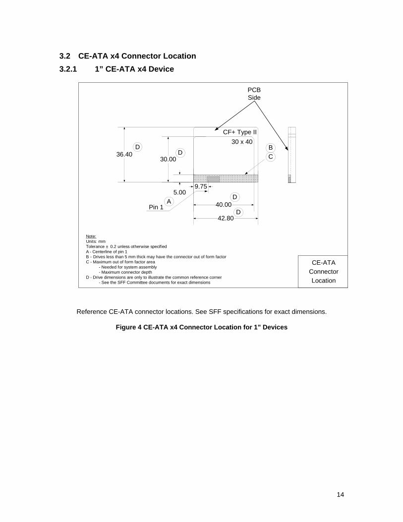
3 CE-ATA x4 Embedded Cable & Connector 3.1 CE-ATA x4 Cable Mating Interface The connection interface of the flex cable is defined in Figure 2. The flex cable shall be 0.3 ± 0.03 mm thick in the 2.5 min. area.
Note:Units: mmTolerance ± 0.2 unless otherwise specifiedA - Centerline of pin 1B - Drives less than 5 mm thick may have the connector out of form factorC - Maximum out of form factor area
- Needed for system assembly- Maximum connector depth
D - Drive dimensions are only to illustrate the common reference corner- See the SFF Committee documents for exact dimensions
CE-ATAConnectorLocation
D
PCBSide
A
30 x 40
42.80
40.00
5.009.75
30.0036.40
D
DD
CB
Reference CE-ATA connector locations. See SFF specifications for exact dimensions.
Figure 4 CE-ATA x4 Connector Location for 1” Devices
14
3.2.2 30mm x 40mm CE-ATA x4 device
Reference CE-ATA connector location. See SFF specifications for exact dimensions.
Figure 5 CE-ATA x4 Connector Location for 30mm x 40mm Devices
15
3.2.3 1.8” CE-ATA x4 Device
Reference CE-ATA connector location. See SFF specifications for exact dimensions.
Figure 6 CE-ATA x4 Connector Location for 1.8” Device
16
4 CE-ATA x8 Embedded Cable and Connector: 4.1 CE-ATA x8 Cable Mating Interface CE-ATA x8 cable shall have pin 1 identified on the cable. FPC thickness is 0.2 +- 0.03 mm. The recommended plating of FPC is gold over nickel plating.
Figure 7 CE-ATA x8 FPC Mating Interface
17
4.2 CE-ATA x8 Connector Location
4.2.1 1” CE-ATA x8 Device
CF+ Type II
Pin 1
Note:Units: mmTolerance ± 0.2 unless otherwise specifiedA - Centerline of pin 1B - Drives less than 5 mm thick may have the connector out of form factorC - Maximum out of form factor area
- Needed for system assembly- Maximum connector depth
D - Drive dimensions are only to illustrate the common reference corner- See the SFF Committee documents for exact dimensions
CE-ATAConnectorLocation
D
PCBSide
A
30 x 40
42.80
40.00
5.009.75
30.0036.40
D
DD
CB
Reference CE-ATA connector location. See SFF specifications for exact dimensions.
Figure 8 CE-ATA x8 Connector Location for 1” Devices
18
4.2.2 1.8” CE-ATA x8 Device
Reference CE-ATA connector location. See SFF specifications for exact dimensions.
Figure 9 CE-ATA x8 Connector Location for 1.8” Devices
19
4.3 CE-ATA x8 Connector 4.3.1 CE-ATA x8 Mid Mount Connector
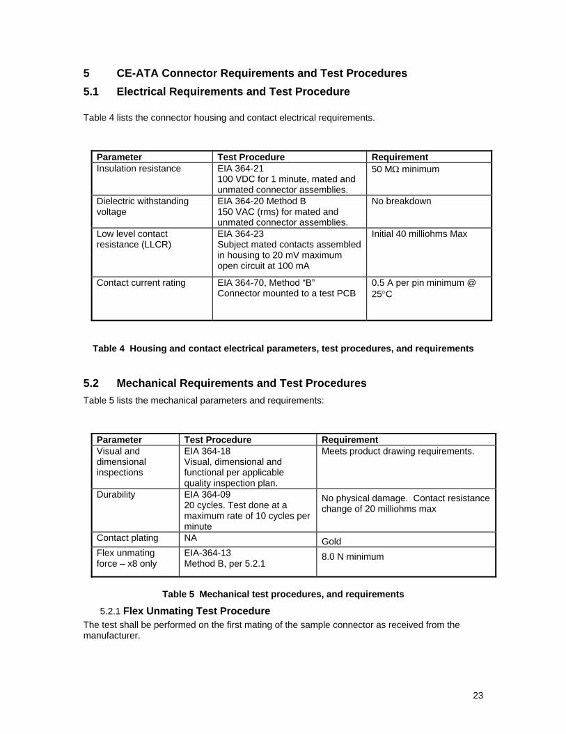
5 CE-ATA Connector Requirements and Test Procedures 5.1 Electrical Requirements and Test Procedure
Table 4 lists the connector housing and contact electrical requirements.
Parameter Test Procedure Requirement Insulation resistance EIA 364-21
100 VDC for 1 minute, mated and unmated connector assemblies.
50 MΩ minimum
Dielectric withstanding voltage
EIA 364-20 Method B 150 VAC (rms) for mated and unmated connector assemblies.
No breakdown
Low level contact resistance (LLCR)
EIA 364-23 Subject mated contacts assembled in housing to 20 mV maximum open circuit at 100 mA
Initial 40 milliohms Max
Contact current rating
EIA 364-70, Method “B” Connector mounted to a test PCB
0.5 A per pin minimum @ 25°C
Table 4 Housing and contact electrical parameters, test procedures, and requirements
5.2 Mechanical Requirements and Test Procedures Table 5 lists the mechanical parameters and requirements:
Parameter Test Procedure Requirement Visual and dimensional inspections
EIA 364-18 Visual, dimensional and functional per applicable quality inspection plan.
Meets product drawing requirements.
Durability EIA 364-09 20 cycles. Test done at a maximum rate of 10 cycles per minute
No physical damage. Contact resistance change of 20 milliohms max
Contact plating NA Gold Flex unmating force – x8 only
EIA-364-13 Method B, per 5.2.1
8.0 N minimum
Table 5 Mechanical test procedures, and requirements
5.2.1 Flex Unmating Test Procedure The test shall be performed on the first mating of the sample connector as received from the manufacturer.
23
The flex circuit shall be designed per Figure 7. The thickness shall be 0.17 + 0.01/-0.00mm and the width shall be 10.05 +0.0/-0.05mm. (The minimum flex thickness and width are used for this test as they provide a worst case condition for retention.) The latch shall be activated. Tests shall be performed for horizontal and vertical unmating force (different connector sample for each test).
Horizontal test: Apply force to the flex such that it is pulled parallel to the plane of the connector mating interface. Vertical test: Apply force to the flex such that it is pulled perpendicular to the plane of the connector mating interface and toward the latching cover of the connector.