Cable networks for television signals, sound signals and interactive services
Part 9: Interfaces for CATV/SMATV headends and similar professional equipment for DVB/MPEG-2 transport streams
Réseaux de distribution par câbles destinés aux signaux de radiodiffusion sonore, de télévision et aux services interactifs Partie 9: Interfaces pour les têtes de résaux pour antennes communautaires, antennes collectives par satellite et matériels professionnels analogues pour les flux transport DVB/MPEG-2
Kabelnetze für Fernsehsignale, Tonsignale und interaktive Dienste Teil 9: Schnittstellen für CATV-/SMATV-Kopfstellen und vergleichbare professionelle Geräte für DVB/MPEG-2-Transportströme
This European Standard was approved by CENELEC on 2002-07-01. CENELEC members are bound to comply with the CEN/CENELEC Internal Regulations which stipulate the conditions for giving this European Standard the status of a national standard without any alteration. Up-to-date lists and bibliographical references concerning such national standards may be obtained on application to the Central Secretariat or to any CENELEC member. This European Standard exists in three official versions (English, French, German). A version in any other language made by translation under the responsibility of a CENELEC member into its own language and notified to the Central Secretariat has the same status as the official versions. CENELEC members are the national electrotechnical committees of Austria, Belgium, Czech Republic, Denmark, Finland, France, Germany, Greece, Hungary, Iceland, Ireland, Italy, Luxembourg, Malta, Netherlands, Norway, Portugal, Slovakia, Spain, Sweden, Switzerland and United Kingdom.
EN 50083-9:2002 - 2 -
Foreword
This European Standard was prepared by CENELEC Technical Committee TC 209, "Cable networks for television signals, sound signals and interactive services" on the basis of EN 50083-9:1998 and a draft amendment to which was submitted to the Unique Acceptance Procedure. The amendment was approved by CENELEC on 2002-07-01 to be published as part of a third edition of EN 50083-9. The following dates were fixed: – latest date by which the EN has to be implemented at national level by publication of an identical national standard or by endorsement
(dop) 2003-07-01
– latest date by which the national standards conflicting with the EN have to be withdrawn
(dow) 2005-07-01
Annexes designated "normative" are part of the body of the standard. Annexes designated "informative" are given for information only. In this standard, annexes A and B are normative and annexes C, D, E, F and G are informative.
__________
- 3 - EN 50083-9: 2002
Contents Page
1 Scope ................................................................................................................................... 5 1.1 General........................................................................................................................... 5 1.2 Specific scope of this part 9............................................................................................ 5
3.1 Terms and definitions ..................................................................................................... 7 3.2 Abbreviations.................................................................................................................. 8
4 Interfaces for MPEG-2 data signals ...................................................................................... 9 4.1 Introduction..................................................................................................................... 8 4.2 Synchronous parallel interface (SPI)............................................................................. 12 4.3 Synchronous Serial Interface (SSI)............................................................................... 17 4.4 Asynchronous Serial Interface (ASI) ............................................................................. 17
Annex A (normative) Synchronous Serial Interface (SSI) ........................................................ 18 Annex B (normative) Asynchronous Serial Interface (ASI) ...................................................... 28 Annex C (informative) 8B/10B tables....................................................................................... 36 Annex D (informative) Implementation guidelines and clock recovery from the Synchronous Serial Interface (SSI) .......................................................................................... 40 Annex E (informative) Implementation guidelines and deriving clocks from the MPEG-2 packets for the ASI ................................................................................................... 44 Annex F (informative) Guidelines for the implementation and usage of the DVB Asynchronous Serial Interface ........................................................................................ 48 Annex G (informative) Bibliography ......................................................................................... 53
Figures Figure 1 - Protocol stack for 188 byte packets ......................................................................... 10 Figure 2 - Protocol stack for 204 byte packets ......................................................................... 10 Figure 3 - Packet structure of 188 byte packet ......................................................................... 10 Figure 4 - Packet structure of 204 byte packet ......................................................................... 10 Figure 5 - System for parallel transmission ............................................................................. 12 Figure 6 - Transmission format with 188 byte packets ............................................................. 13 Figure 7 - Transmission format with 204 byte packets (188 data bytes and 16 dummy bytes) ..................................................................................... 13 Figure 8 - Transmission format with RS-coded packets (204 bytes; 188 data bytes and 16 valid extra bytes) as specified in EN 300 421 ............................................................... 13 Figure 9 - Clock to data timing (at source) ............................................................................... 14 Figure 10 - Line driver and line receiver interconnection .......................................................... 15 Figure 11 - Idealized eye diagramme corresponding to the minimum input signal level ....................................................................................................... 16 Figure A.1 - Example of cascaded interfaces ........................................................................... 18
EN 50083-9:2002 - 4 - Figure A.2 - Coaxial cable-based synchronous serial transmission link (SSI type)....................19 Figure A.3 - Fibre-optic-based synchronous serial transmission link (SSI type) ........................19 Figure A.4 - Pulse mask for logical 0 ........................................................................................22 Figure A.5 - Pulse mask for logical 1 ........................................................................................23 Figure A.6 - Biphase Mark encoding.........................................................................................26 Figure B.1 - Coaxial cable-based asynchronous serial transmission link (ASI type)..................28 Figure B.2 - Fibre-optic-based asynchronous serial transmission link (ASI type) ......................29 Figure B.3 - Serial link Layer-0 reference points .......................................................................30 Figure B.4 - Coaxial transmitter test circuit ...............................................................................31 Figure B.5 - Transmitter eye diagramme for jitter......................................................................32 Figure B.6 - Spectral width of transmitter ..................................................................................33 Figure B.7 - Transmission format with data packets (example for 188 bytes) ...........................35 Figure B.8 - Transmission format with data bursts (example for 188 bytes)..............................35 Figure D.1 - Connection of the adapter modules ......................................................................40 Figure D.2 - Example of implementation of an emitting module ................................................41 Figure D.3 - Example of implementation of a receiving module ................................................42 Figure D.4 - Example of implementation of a flexible data rate receiving module for SSI ............. Figure E.1 - ASI link with output clock from following application or alternative with clock recovery...........................................................................................................................44 Figure E.2 - Phase Locked Loop for clock generation...............................................................45
Figure F.1 - Abstract ASI transmission model...........................................................................48 Figure F.2 - Random aperiodic transport stream rate and buffer utilisation...............................50 Figure F.3 - Deterministic aperiodic transport stream rate and buffer utilisation........................50
Tables Table 1 - Mandatory and optional packet lengths......................................................................11 Table 2 - Contact assignment of 25 contact type D subminiature connector (ISO 2110) ..........17 Table A.1 - Transmitter output characteristics...........................................................................21 Table A.2 - Receiver input characteristics.................................................................................21 Table A.3 - Optical characteristics for SSI links ........................................................................24 Table B.1 - Electrical characteristic specifications for ASI link ..................................................31 Table B.2 - Chromatic dispersion requirements ........................................................................32 Table B.3 - Optical characteristic specifications for ASI link......................................................33 Table C.1 - Valid data characters..............................................................................................36 Table C.2 - Valid special characters .........................................................................................38 Table C.3 - Delayed code violation example .............................................................................39
Table E.2 - Analysis of 10 kHz clock generating loop, ± 2 ms jitter ...........................................47
- 5 - EN 50083-9: 2002 1 Scope
1.1 General
Standards of EN 50083 series deal with cable networks for television signals, sound signals and interactive services including equipment, systems and installations
• for headend reception, processing and distribution of television and sound signals and their associated data signals and
• for processing, interfacing and transmitting all kinds of signals for interactive services using all applicable transmission media. All kinds of networks like
• CATV-networks, • MATV-networks and SMATV-networks, • Individual receiving networks
and all kinds of equipment, systems and installations installed in such networks, are within this scope. The extent of this standardization work is from the antennas, special signal source inputs to the headend or other interface points to the network up to the system outlet or the terminal input, where no system outlet exists. The standardization of any user terminals (i.e. tuners, receivers, decoders, multimedia terminals etc.) as well as of any coaxial and optical cables and accessories therefor is excluded.
1.2 Specific scope of this part 9
This standard describes physical interfaces for the interconnection of signal processing devices for professional CATV/SMATV headend equipment or for similar systems, such as in uplink stations. Especially this document specifies the transfer of DVB/MPEG-2 data signals in the standardized transport layer format between devices of different signal processing functions. RF interfaces and interfaces to telecom networks are not covered in this document. In addition references are made to all other parts of EN 50083 series (Cable networks for television signals, sound signals and interactive services) and in particular for RF, video and audio interfaces to part 5: "Headend equipment“. For connections to telecom networks a special Data Communication Equipment (DCE) is necessary to adapt the serial or parallel interfaces specified in this document to the bitrates and transmission formats of the public Plesiochronic Digital Hierarchy (PDH) networks. Other emerging technologies such as Connectionless Broadband Data Services (CBDS), Synchronous Digital Hierarchy (SDH), Asynchronous Transfer Mode (ATM) etc. can be used for transmitting MPEG-2 Transport Streams (TS) between remote locations. ATM is particularly suitable for providing bandwidth on demand and it allows for high data rates.
EN 50083-9:2002 - 6 - 2 Normative references
This European Standard incorporates by dated or undated reference, provisions from other publications. These normative references are cited at the appropriate places in the text and the publications are listed hereafter. For dated references, subsequent amendments to or revisions of any of these publications apply to this European Standard only when incorporated in it by amendment or revision. For undated references the latest edition of the publication referred to applies. EN 50083 Cable networks for television signals, sound signals and
interactive services EN 50083-1 1993 Part 1: Safety requirements + A1 1997 + A2 1997 EN 50083-2 2001 Part 2: Electromagnetic compatibility for equipment EN 50083-3 2002 Part 3: Active wideband equipment for coaxial cable networks EN 50083-4 1998 Part 4: Passive wideband equipment for coaxial cable networks EN 50083-5 2001 Part 5: Headend equipment EN 50083-6 1997 Part 6: Optical equipment EN 50083-7 1996 Part 7: System performance + A1 2000 EN 50083-8 2002 Part 8: Electromagnetic compatibility for networks EN 60793-2-10 2002 Optical fibres - Part 2-10: Product specifications - Sectional
specification for category A1 multimode fibres (IEC 60793-2-10:2002)
EN 60793-2-50 2002 Optical fibres - Part 2-50: Product specifications - Sectional
specification for class B single-mode fibres (IEC 60793-2-50:2002)
EN ISO/IEC 13818-1 1997 Information technology - Generic coding of moving pictures and
associated audio information - Part 1: Systems (ISO/IEC 13818-1:1996)
EN ISO/IEC 13818-9 2000 Information technology - Generic coding of moving pictures and
associated audio information - Part 9: Extension for real-time interface for systems decoders (ISO/IEC 13818-9:1996)
EN 300 421 1997 Digital Video Broadcasting (DVB) - Framing structure, channel
coding and modulation for 11/12 GHz satellite services EN 300 429 1997 Digital Video Broadcasting (DVB) - Framing structure, channel
coding and modulation for cable systems
- 7 - EN 50083-9: 2002 EN 300 473 1997 Digital Video Broadcasting (DVB) - Satellite Master Antenna
Television (SMATV) distribution systems ETR 290 1997 Digital Video Broadcasting (DVB) - Measurement guidelines for
DVB systems IEC 60169-8 1978 Radio frequency connectors - Part 8: RF coaxial connectors with
inner diameter of outer conductor 6,5 mm (0,25 in) with bayonet lock - Characteristic impedance 50 Ω (type BNC)
IEC 60793-2 series Optical fibres - Part 2: Product specifications IEC 60874-14 1993 Connectors for optical fibres and cables - Part 14: Sectional
specification for fibre-optic connector - Type SC ISO 2110 1989 Information technology - Data communication, 25 pole DTE/DCE
interface connector and contact number assignments ISO/IEC 14165-111 1) Information technology - Fibre Channel - Part 111: Physical and
signalling interface (FC-PH) ITU-R Rec. BT.656-4 1998 Interfaces for digital component video signals in 525-line and
625-line television systems operating at the 4:2:2 level of recommendation ITU-R BT.601
ITU-T Rec. G.654 2002 Characteristics of cut-off shifted single-mode optical fibre and
cable ITU-T Rec. G.703 2001 Physical/electrical characteristics of hierarchical digital interfaces ITU-T Rec. G.957 1999 Optical interfaces for equipments and systems relating to the
synchronous digital hierarchy 3 Terms, definitions and abbreviations 3.1 Terms and definitions 3.1.1 headend equipment which is connected between receiving antennas or other signal sources and the remainder of the cable distribution system to process the signals to be distributed NOTE The headend may, for example, comprise antenna amplifiers, frequency converters, combiners, selectors and generators. 3.1.2 Satellite Master Antenna Television system (SMATV) a system which is designed to provide sound and television signals to the households of a building or group of buildings
1) In preparation
EN 50083-9:2002 - 8 - NOTE Two system configurations are defined in EN 300 473 as follows: - SMATV system A, based on transparent transmodulation of QPSK satellite signals into QAM signals to be
distributed to the user - SMATV system B, based on direct distribution of QPSK signals to the user, with two options: - SMATV-IF distribution in the satellite IF band (above 950 MHz) - SMATV-S distribution in the VHF/UHF band, for example in the extended S-band (230-470 MHz) 3.1.3 Biphase Mark a line code which ensures DC balance, easy clock recovery and polarity freedom 3.1.4 Transport Stream includes one or more programs with one or more independent time bases into a single stream. The Transport Stream is designed for use in environments where errors are likely, such as storage or transmission in lossy or noisy media. 3.1.5 Transport Packet a packetized element of the Transport Stream. The packets are either 188 bytes or in case of using Reed Solomon FEC 204 byte in length 3.1.6 DVALID a signal which indicates in the 204 byte mode of a Transport Stream that the empty space is filled with dummy bytes 3.1.7 PSYNC A flag which indicates the beginning of a packet 3.2 Abbreviations 8B/10B eight to ten bit conversion ACCP Accumulated Phase ACCT Accumulated Time ASI Asynchronous Serial Interface ASI-C Asynchronous Serial Interface on coacial cable ASI-O Asynchronous Serial Interface on opticaL fiber ATM Asynchronous Transfer Mode BER Bit Error Rate CBDS Connectionless Broadband Data Services DFB Distributed Feedback DJ Deterministic Jitter DVALID data valid DVB Digital Video Broadcast FC FIBRE Channel FEC Forward Error Correction FIFO First In First Out FWHM Full Width Half Max IEC International Electrotechnical Commission ISO International Standards Organisation ITU-R International Telecommunication Union Radiocommunication ITU-T International Telecommunication Union Telecommunication LF Low Frequency
- 9 - EN 50083-9: 2002 LVDS Low Voltage Differential Signalling MPEG Motion Picture Experts Group MSB Most Significant Bit NA not applicable NRZ Non-Return-to-Zero NTSC National Television System Committee PAL Phase Alternation Line PCR Program Clock Reference PDH Plesiosynchronic Digital Hierarchy PLL Phase Lock Loop PMD Physical Medium Dependent PSYNC Packet Synchron QAM Quadrature Amplitude Modulation QPSK Quarternary Phase Shift Keying RB Receiver Buffer RD Running Disparity RIN Relative Intrinsic Noise RJ Random Jitter RS Reed Solomon rx-clk receiver clock SDH Synchronous Digital Hierarchy SMPT Society of Motion Picture and Television Engineers SPI Synchronous Parallel Interface SSI Synchronous Serial Interface SSI-C Synchronous Serial Interface on coacial cable SSI-O Synchronous Serial Interface on optical fiber TB Transmission Buffer Tr rise-time TS Transport Stream tx-clk transmission clock UNC Unified National Coarse Thread NOTE Only the abbreviations used in the English version of this part of EN 50083 are mentioned in this subclause. The German and the French versions of this part may use other abbreviations. Refer to 3.2 of each language version for details. 4 Interfaces for MPEG-2 data signals
4.1 Introduction
This subclause describes possible interfaces for devices transmitting or receiving MPEG-2 data as transport packets, such as QPSK demodulators, QAM modulators, multiplexers, demultiplexers, or telecom network adapters. This specification is similar to EN 300 429 and EN 300 421. NOTE Both standards describe a first functional block representing the MPEG2 source coding and multiplexing as standardised in EN ISO/IEC 13818-1, a second functional block representing the channel adaptation, whereas an interface in between shall be based on MPEG2 transport stream specification as per EN ISO/IEC 13818-1. The function of the channel modulator/demodulator is to adapt the signal to the characteristics of the transmission channel: satellite, terrestrial or cable as specified in the DVB base line documents.
EN 50083-9:2002 - 10 - Also the case where data signals are transmitted to or from a headend via a telecom network or if a headend serves to insert data signals into such networks is considered to be covered by the generic channel modulator / demodulator functional block. The interface parameters valid for this network have to be met. For the latter reference is made to ITU-T G.703 for Plesiochronic Digital Hierarchy (PDH) networks.
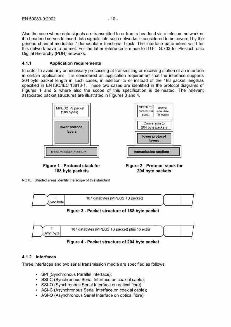
4.1.1 Application requirements In order to avoid any unnecessary processing at transmitting or receiving station of an interface in certain applications, it is considered an application requirement that the interface supports 204 byte packet length in such cases, in addition to or instead of the 188 packet lengthas specified in EN ISO/IEC 13818-1. These two cases are identified in the protocol diagrams of Figures 1 and 2 where also the scope of this specification is delineated. The relevant associated packet structures are illustrated in Figures 3 and 4.
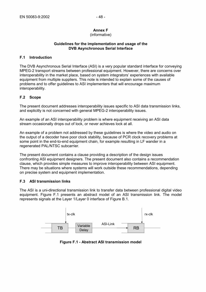
transmission medium
lower protocollayers
MPEG2 TS packet(188 bytes)
MPEG2 TSpacket (188
bytes)
optionalextra data(16 bytes)
transmission medium
lower protocollayers
Conversion to204 byte packets
Figure 1 - Protocol stack for Figure 2 - Protocol stack for 188 byte packets 204 byte packets NOTE Shaded areas identify the scope of this standard
187 databytes (MPEG2 TS packet)1Sync byte
Figure 3 - Packet structure of 188 byte packet
1Sync byte
187 databytes (MPEG2 TS packet) plus 16 extra
Figure 4 - Packet structure of 204 byte packet
4.1.2 Interfaces Three interfaces and two serial transmission media are specified as follows:
• SPI (Synchronous Parallel Interface); • SSI-C (Synchronous Serial Interface on coaxial cable); • SSI-O (Synchronous Serial Interface on optical fibre); • ASI-C (Asynchronous Serial Interface on coaxial cable); • ASI-O (Asynchronous Serial Interface on optical fibre).
- 11 - EN 50083-9: 2002 Each of these interfaces feature a BER such that FEC is not required for reliable data transport. The synchronous parallel interface is specified to cover short or medium distances, i.e. for devices arranged near to each other. Subclause 4.2 describes the definitions for such a parallel interface derived from ITU-R Recommendation BT.656-4. Flags are provided to distinguish 188 byte packets from 204 byte packets, and to signal the existence of valid RS bytes. Note that the interface as such is transparent to the RS bytes. The synchronous serial interface (SSI) which can be seen as an extension of the parallel interface, is briefly introduced in subclause 4.3 and described in detail in annexes A and D. The packet length and the existence of valid RS bytes are conveyed through suitable coding mechanisms. Subclause 4.4 introduces the Asynchronous Serial Interface (ASI). Details of the ASI are provided in annexes B and E. The ASI is configurable to either convey 188 byte packets (which is mandatory) or optionally 204 byte packets. 4.1.3 Packet length and contents Each of the interface specifications can be used to convey either 188 byte packets or 204 byte packets in order to enable selection of the appropriate interface characteristics dependent on the kind of equipment to be interconnected. Which packet sizes are mandatory and which are optional is specified in Table 1.
Table 1 - Mandatory and optional packet lengths Data packet carrying capability
Interface 188 bytes 204 bytes (with 16 dummy
bytes)
204 bytes (with 16 RS bytes)
SPI transmitter O M O receiver M M M SSI transmitter O M O receiver M M M ASI transmitter M O O receiver M O O M mandatory O optional
In case the data stream is packetised in 188 byte packets and the interface is configured to convey 204 byte packets, the extra packet length can be used for additional data. The contents of the 16 bytes in this extra packet length are not specified in this standard. One application could be the transmission of 16 RS bytes associated with the preceding transport package.
4.1.4 Compliance For an equipment to be compliant to this standard it is sufficient for the equipment to show at least one instance of at least one of the interface specifications as introduced in 4.1.2 and specified in detail in subsequent subclauses of this standard, while at least the mandatory packet sizes as indicated in 4.1.3 shall be supported.
EN 50083-9:2002 - 12 - 4.1.5 System integration The interfaces specified in this standard define physical connections between various pieces of equipment. It is important to notice that various parameters which are important for interoperation are not specified in this standard. This is intentional as it leaves maximum implementation flexibility for different applications. In order to facilitate system integration equipment suppliers shall provide the following information about the characteristics of the interfaces in their equipment:
• Interface type (SPI, SSI-C, SSI-O, ASI-C, ASI-O); • Supported packet length (188 bytes, 204 bytes, both); • Maximum input jitter (jitter measured as specified in EN ISO/IEC 13818-9); • Output jitter (jitter measured as specified in EN ISO/IEC 13818-9); • Minimum input data rate (rate measured as specified in EN ISO/IEC 13818-1); • Maximum input data rate (rate measured as specified in EN ISO/IEC 13818-1).
Some of these parameters may not be applicable to certain types of equipment. If all relevant parameters are provided by equipment suppliers, the proper functioning of the complete system can be ensured.
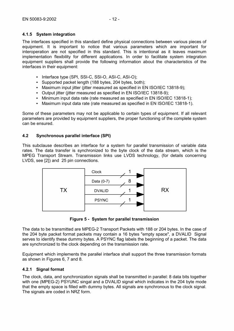
4.2 Synchronous parallel interface (SPI)
This subclause describes an interface for a system for parallel transmission of variable data rates. The data transfer is synchronized to the byte clock of the data stream, which is the MPEG Transport Stream. Transmission links use LVDS technology, (for details concerning LVDS, see [2]) and 25 pin connections.
1
8
1
1
Data (0-7)
Clock
PSYNC
TX RXDVALID
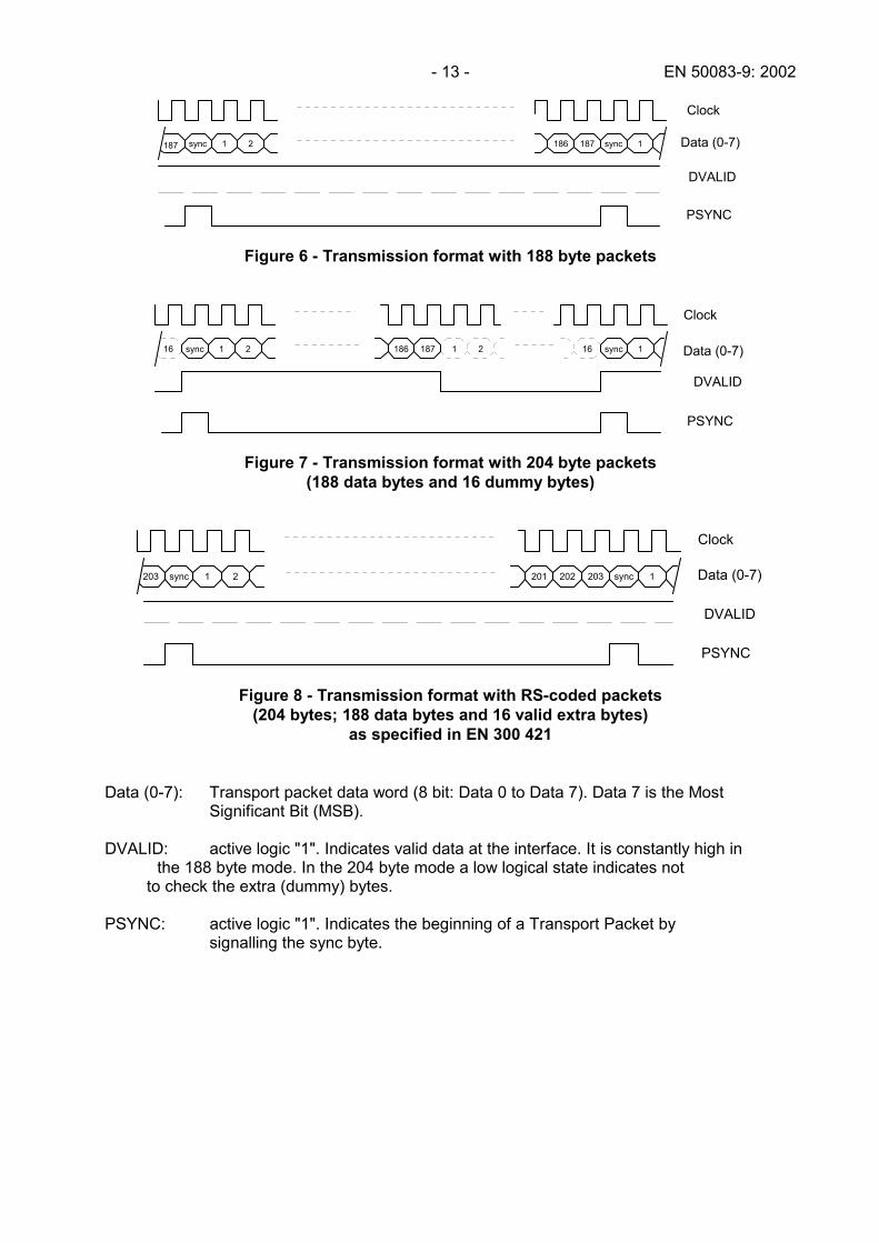
Figure 5 - System for parallel transmission The data to be transmitted are MPEG-2 Transport Packets with 188 or 204 bytes. In the case of the 204 byte packet format packets may contain a 16 bytes "empty space", a DVALID Signal serves to identify these dummy bytes. A PSYNC flag labels the beginning of a packet. The data are synchronized to the clock depending on the transmission rate. Equipment which implements the parallel interface shall support the three transmission formats as shown in Figures 6, 7 and 8. 4.2.1 Signal format The clock, data, and synchronization signals shall be transmitted in parallel: 8 data bits together with one (MPEG-2) PSYUNC singal and a DVALID signal which indicates in the 204 byte mode that the empty space is filled with dummy bytes. All signals are synchronous to the clock signal. The signals are coded in NRZ form.
- 13 - EN 50083-9: 2002
sync
PSYNC
1 2 186 sync 1187187 Data (0-7)
Clock
DVALID
Figure 6 - Transmission format with 188 byte packets
sync
PSYNC
1 2 186 sync 1187 1 2 1616 Data (0-7)
Clock
DVALID
Figure 7 - Transmission format with 204 byte packets (188 data bytes and 16 dummy bytes)
sync
PSYNC
1 2 sync 1203 203202201 Data (0-7)
Clock
DVALID
Figure 8 - Transmission format with RS-coded packets (204 bytes; 188 data bytes and 16 valid extra bytes)
as specified in EN 300 421 Data (0-7): Transport packet data word (8 bit: Data 0 to Data 7). Data 7 is the Most Significant Bit (MSB). DVALID: active logic "1". Indicates valid data at the interface. It is constantly high in the 188 byte mode. In the 204 byte mode a low logical state indicates not to check the extra (dummy) bytes. PSYNC: active logic "1". Indicates the beginning of a Transport Packet by signalling the sync byte.
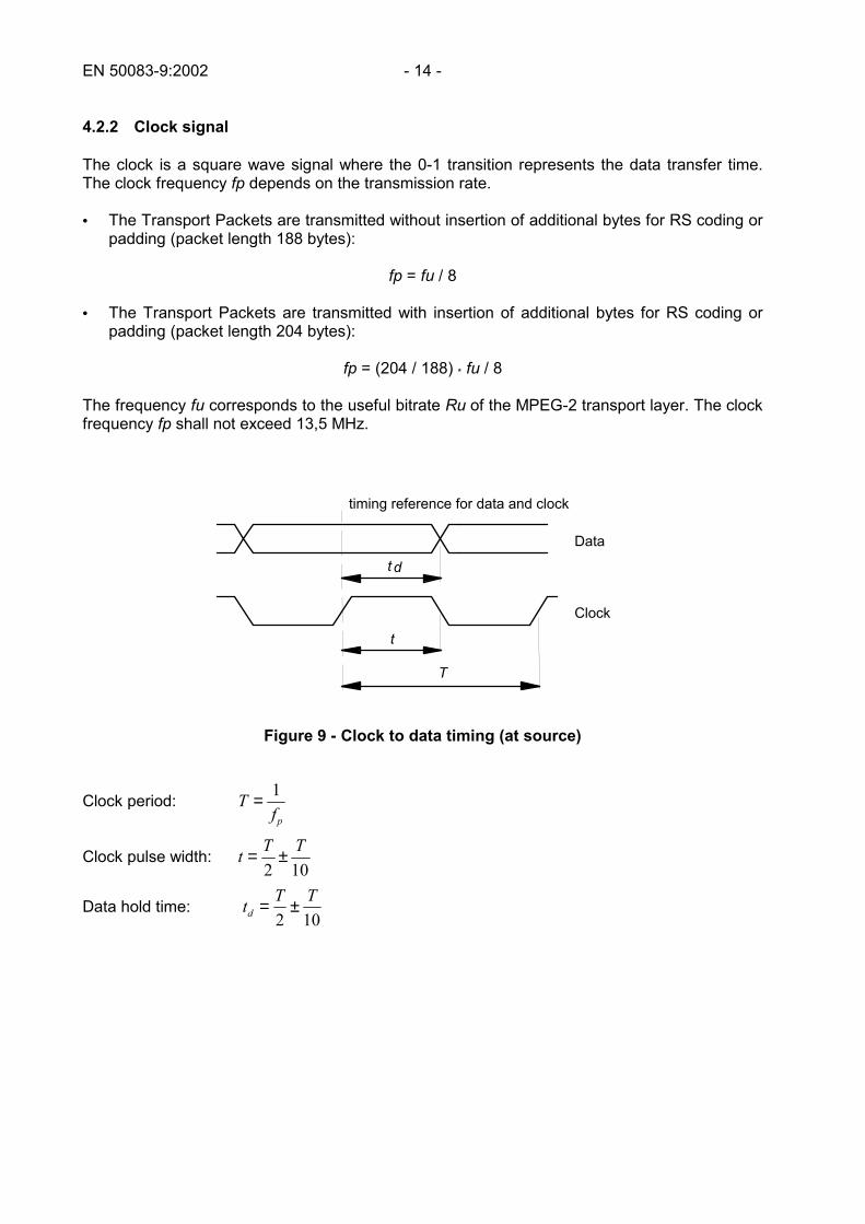
EN 50083-9:2002 - 14 - 4.2.2 Clock signal The clock is a square wave signal where the 0-1 transition represents the data transfer time. The clock frequency fp depends on the transmission rate. • The Transport Packets are transmitted without insertion of additional bytes for RS coding or
padding (packet length 188 bytes):
fp = fu / 8 • The Transport Packets are transmitted with insertion of additional bytes for RS coding or
padding (packet length 204 bytes):
fp = (204 / 188) * fu / 8 The frequency fu corresponds to the useful bitrate Ru of the MPEG-2 transport layer. The clock frequency fp shall not exceed 13,5 MHz.
Data
Clock
t d
t
T
timing reference for data and clock
Figure 9 - Clock to data timing (at source)
Clock period: Tfp
= 1
Clock pulse width: t T T= ±2 10
Data hold time: t T Td = ±
2 10
- 15 - EN 50083-9: 2002 4.2.3 Electrical characteristics of the interface The interface employs eleven line drivers and eleven line receivers. Each line driver (source) has a balanced output and the corresponding line receiver (destination) a balanced input (see Figure 10). The line driver and receiver shall be LVDS-compatible, i.e. they shall permit the use of LVDS for their drivers or receivers. All digital signal time intervals are measured between the half-amplitude points. Logic convention The terminal A of the line driver is positive with respect to the terminal B for a binary 1 and negative for a binary 0 (see Figure 10).
Source Destination
Linereceiver
Linedriver
Transmissionline
A
B
A'
B'
Z =t100 Ω
Figure 10 - Line driver and line receiver interconnection
Line driver characteristics (source) Output impedance: 100 Ω maximum Common mode voltage: 1,125 V to 1,375 V Signal amplitude: 247 mV to 454 mV Rise and fall times: less than T / 7, measured between the 20% and 80% amplitude points, with a 100 Ω resistive load. The difference between rise and fall times shall not exceed T / 20. Line receiver characteristics (destination) Input impedance: 90 Ω to 132 Ω Maximum input signal: 2,0 V peak to peak Minimum input signal: 100 mV peak to peak
EN 50083-9:2002 - 16 - However, the line receiver shall sense correctly the binary data when a random data signal produces the conditions represented by the eye diagramme in Figure 11 at the data detection point. Maximum common mode signal: ± 0,5 V, comprising interference in the range of 0 to 15 kHz (both terminals to ground). Differential delay: Data shall be correctly sensed when the clock-to-data differential delay is in the range between ± T / 3 (see Figure 11).
Umin
Tmin
Tmin
reference transition of clock
Tmin = T / 3, Umin = 100 mV
Figure 11 - Idealized eye diagramme corresponding to the minimum input signal level
4.2.4 Mechanical details of the connector The interface uses the 25 contact type D subminiature connector specified in ISO 2110 with the contact assignment shown in Table 2. Connectors are locked together with screw lock, with male screws on the cable connector and a female threaded posts on the equipment connector. The threads are of type UNC 4-40 [3]. Cable connectors employ pin contacts and equipment connectors employ socket contacts. Shielding of the interconnecting cable and its connectors shall be employed.
- 17 - EN 50083-9: 2002
Table 2 - Contact assignment of 25 contact type D subminiature connector
(ISO 2110)
Pin Signal line Pin Signal line
1 2 3 4 5 6 7 8 9 10 11 12 13
Clock A System Gnd Data 7 A(MSB) Data 6 A Data 5 A Data 4 A Data 3 A Data 2 A Data 1 A Data 0 A DVALID A PSYNC A Cable Shield
14 15 16 17 18 19 20 21 22 23 24 25
Clock B System Gnd Data 7 B Data 6 B Data 5 B Data 4 B Data 3 B Data 2 B Data 1 B Data 0 B DVALID B PSYNC B
4.3 Synchronous Serial Interface (SSI) The Synchronous Serial Interface (SSI) can be seen as the extension of the parallel interface by means of an adaptation of the parallel format. SSI is synchronous to the Transport Stream which is transmitted on the serial link. A detailed specification of the SSI is provided in annex A and guidelines for its implementation are provided in annex D. 4.4 Asynchronous Serial Interface (ASI) The Asynchronous Serial Interface (ASI) is a serial link operating at a fixed line clock rate. A detailed specification of ASI is provided in normative annex B. Implementation guidelines and deriving clocks from the MPEG-2 packets for ASI are provided in informative annex E. Guidelines for the implementation and usage of ASI are laid down in informative annex F.
EN 50083-9:2002 - 18 -
Annex A (normative)
Synchronous Serial Interface (SSI)
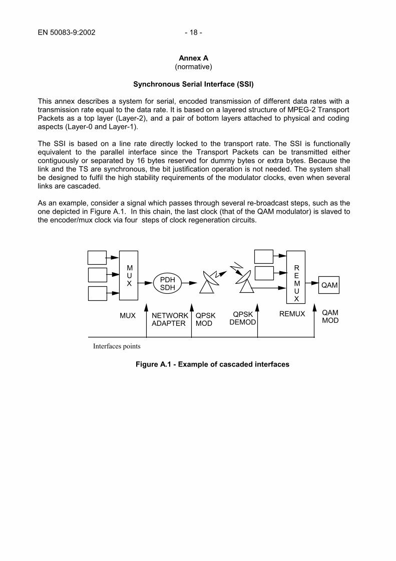
This annex describes a system for serial, encoded transmission of different data rates with a transmission rate equal to the data rate. It is based on a layered structure of MPEG-2 Transport Packets as a top layer (Layer-2), and a pair of bottom layers attached to physical and coding aspects (Layer-0 and Layer-1). The SSI is based on a line rate directly locked to the transport rate. The SSI is functionally equivalent to the parallel interface since the Transport Packets can be transmitted either contiguously or separated by 16 bytes reserved for dummy bytes or extra bytes. Because the link and the TS are synchronous, the bit justification operation is not needed. The system shall be designed to fulfil the high stability requirements of the modulator clocks, even when several links are cascaded. As an example, consider a signal which passes through several re-broadcast steps, such as the one depicted in Figure A.1. In this chain, the last clock (that of the QAM modulator) is slaved to the encoder/mux clock via four steps of clock regeneration circuits.
M U X PDH
SDH
R EM U X
QAM
Interfaces points
QPSK MOD
QPSK DEMOD
QAMMOD
REMUXNETWORK ADAPTER
MUX
Figure A.1 - Example of cascaded interfaces
- 19 - EN 50083-9: 2002 A.1 SSI transmission system overview Figures A.2 and A.3 represent the primary components of this SSI method over copper coaxial cable and fibre-optic cable, respectively.
Figure A.2 - Coaxial cable-based synchronous serial transmission link (SSI type)
Figure A.3 - Fibre-optic-based synchronous serial transmission link (SSI type)
The main functions of the transmission system are described below. Emission path Data to be transmitted are presented in byte-synchronized form as MPEG-2 Transport Packets. The Transport Stream is then passed through a parallel-to-serial converter. The line data stream is locked to the TS data stream. The serial signal is Biphase Mark encoded.
Fibre-OpticCable
Continuous Byte-
Synchronous
Continuous Byte-Synchronous MPEG-2 TS
Layer-1
Layer-0Layer-2
Parallel/Serial Conversion Biphase
Coding Amplifier/
Buffer Connector
Serial/Parallel Conversion
Amplifier/ Buffer Connector
Optical Emitter
Optical Receiver
Clock Recovery Biphase
Coaxial Cable
Continuous Byte-
Synchronous
Continuous Byte-Synchronous MPEG-2 TS
Layer-1
Layer-0Layer-2
Parallel/Serial Conversion
Biphase Coding
Amplifier/ Buffer
Coupling/ Impedance Matching
Connector
Serial/Parallel Conversion
Amplifier/ Buffer
Coupling/ Impedance Matching
Connector Clock
Recovery Biphase
EN 50083-9:2002 - 20 - In the case of a coaxial cable application, the resulting signal is typically passed to a buffer/ driver circuit and then through a coupling network, which performs impedance matching and optionally galvanic isolation, to a coaxial connector. In the case of fibre-optic application, the serial bit stream is passed through a driver circuit which drives an optical transmitter (LED or LASER) which is coupled to a fibre-optic cable through a connector. Reception path The incoming data stream from the coaxial cable is first coupled through a connector and coupling network to a circuit which recovers clock and data. In case of fibre-optic transmission, a light sensitive detector converts light levels to electrical levels which then are passed to a clock and data recovery circuit. Once the clock and data are recovered, the bit stream is passed to a Biphase Mark decoder. In order to recover byte alignment, a decoder searches in the serial stream for the synchronization word which is necessary to achieve the serial to parallel conversion. Annex D provides further clarification of the characteristics of the SSI and implementation guidelines for clock and data recovery. A.2 SSI configuration A SSI interconnection physically consists of two nodes: a transmitting node and a receiving node. This unidirectional optical fibre or copper coaxial cable carrying data from the transmitting node to the receiving node is referred to as a link. The link is used by the interconnected ports to perform communication. Physical equipment such as video or audio compressors, multiplexers, modulators, etc., can be interconnected through these links. This SSI specification clause applies only to the point-to-point type link. A.3 SSI protocol architecture description The SSI protocol is divided into three architectural layers for purposes of development of the standard: Layer-0, Layer-1, Layer-2. A.3.1 Layer-0: Physical requirements The physical layer defines the transmission media, the drivers and receivers. The transmission uses Biphase Mark encoding. This subclause provides specifications for SSI physical layer (Layer-0). Interfaces for coaxial and optical fibre applications are specified. The links are unidirectional point to point. A.3.1.1 Coaxial cable Physical Medium Dependent (PMD) requirement The nominal cable impedance shall be 75 Ω. Considering that the transmission data rate is derived from the user data rate, longer links can be achieved for lower user data rates. The physical medium specified in this subclause has the following characteristics: - Provides a means of coupling the SSI Layer-1 to the coaxial cable segment - Provides the driving of coaxial cable between a transmitter and a receiver - Specifies the type and grade of cable and connectors to be used in a synchronous
serial interface link.
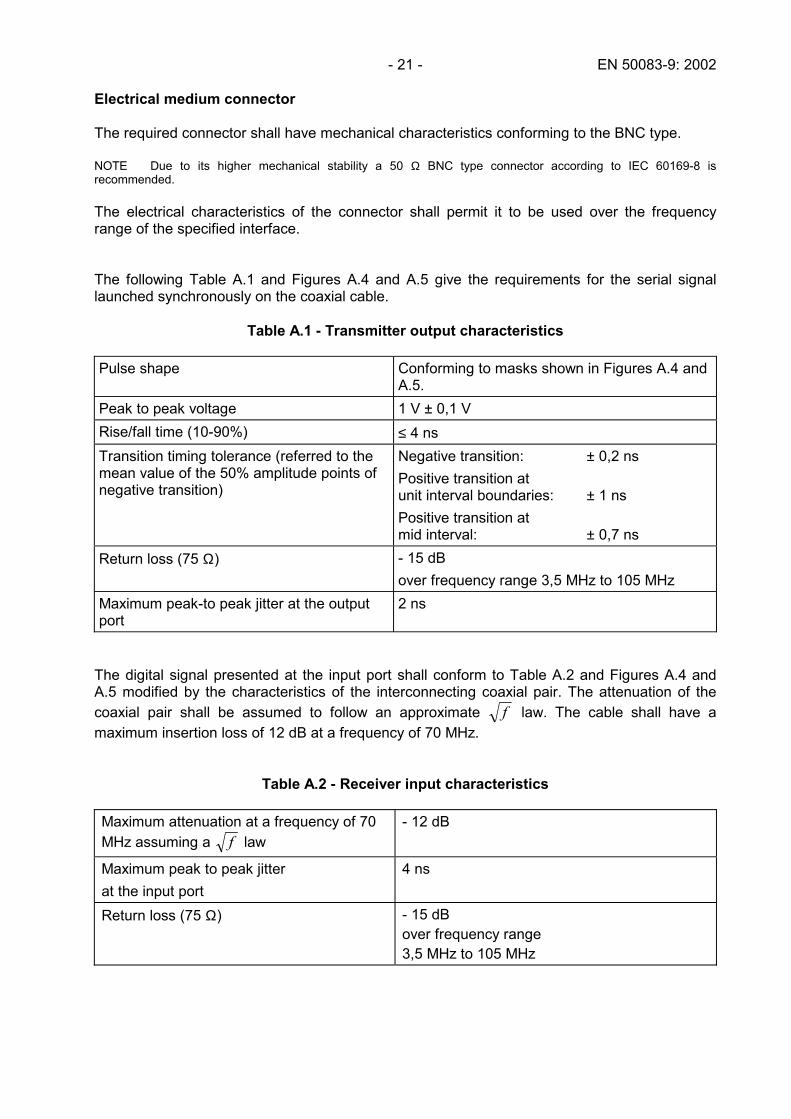
- 21 - EN 50083-9: 2002 Electrical medium connector The required connector shall have mechanical characteristics conforming to the BNC type. NOTE Due to its higher mechanical stability a 50 Ω BNC type connector according to IEC 60169-8 is recommended. The electrical characteristics of the connector shall permit it to be used over the frequency range of the specified interface. The following Table A.1 and Figures A.4 and A.5 give the requirements for the serial signal launched synchronously on the coaxial cable.
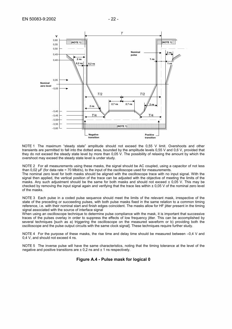
Table A.1 - Transmitter output characteristics Pulse shape Conforming to masks shown in Figures A.4 and
A.5. Peak to peak voltage 1 V ± 0,1 V Rise/fall time (10-90%) ≤ 4 ns Transition timing tolerance (referred to the mean value of the 50% amplitude points of negative transition)
Negative transition: ± 0,2 ns Positive transition at unit interval boundaries: ± 1 ns Positive transition at mid interval: ± 0,7 ns
Return loss (75 Ω) - 15 dB over frequency range 3,5 MHz to 105 MHz
Maximum peak-to peak jitter at the output port
2 ns
The digital signal presented at the input port shall conform to Table A.2 and Figures A.4 and A.5 modified by the characteristics of the interconnecting coaxial pair. The attenuation of the coaxial pair shall be assumed to follow an approximate f law. The cable shall have a maximum insertion loss of 12 dB at a frequency of 70 MHz.
Table A.2 - Receiver input characteristics Maximum attenuation at a frequency of 70 MHz assuming a f law
- 12 dB
Maximum peak to peak jitter at the input port
4 ns
Return loss (75 Ω) - 15 dB over frequency range 3,5 MHz to 105 MHz
EN 50083-9:2002 - 22 -
- 0,60
- 0,55
- 0,50
- 0,45
- 0,40
0,60
0,55
0,50
0,45
0,40
Negativetransition
Positivetransition
2,7 ns 2,7 ns
Nominalzero level
V
Nominal pulse
T
2 ns
2 ns
0,2 ns0,2 ns
1 ns
1 ns
2 ns
2 ns
(NOTE 1)(NOTE 1)
(NOTE 1)
0,05
- 0,05
/4T/4T
/2T /2T
NOTE 1 The maximum “steady state” amplitude should not exceed the 0,55 V limit. Overshoots and other transients are permitted to fall into the dotted area, bounded by the amplitude levels 0,55 V and 0,6 V, provided that they do not exceed the steady state level by more than 0,05 V. The possibility of relaxing the amount by which the overshoot may exceed the steady state level is under study. NOTE 2 For all measurements using these masks, the signal should be AC coupled, using a capacitor of not less than 0,02 µF (for data rate = 70 Mbit/s), to the input of the oscilloscope used for measurements.
The nominal zero level for both masks should be aligned with the oscilloscope trace with no input signal. With the signal then applied, the vertical position of the trace can be adjusted with the objective of meeting the limits of the masks. Any such adjustment should be the same for both masks and should not exceed ± 0,05 V. This may be checked by removing the input signal again and verifying that the trace lies within ± 0,05 V of the nominal zero level of the masks. NOTE 3 Each pulse in a coded pulse sequence should meet the limits of the relevant mask, irrespective of the state of the preceding or succeeding pulses, with both pulse masks fixed in the same relation to a common timing reference, i.e. with their nominal start and finish edges coincident. The masks allow for HF jitter present in the timing signal associated with the source of interface signal
When using an oscilloscope technique to determine pulse compliance with the mask, it is important that successive traces of the pulses overlay in order to suppress the effects of low frequency jitter. This can be accomplished by several techniques [such as a) triggering the oscilloscope on the measured waveform or b) providing both the oscilloscope and the pulse output circuits with the same clock signal]. These techniques require further study. NOTE 4 For the purpose of these masks, the rise time and delay time should be measured between –0,4 V and 0,4 V, and should not exceed 4 ns. NOTE 5 The inverse pulse will have the same characteristics, noting that the timing tolerance at the level of the negative and positive transitions are ± 0,2 ns and ± 1 ns respectively.
Figure A.4 - Pulse mask for logical 0
- 23 - EN 50083-9: 2002
- 0,60
- 0,55
- 0,50
- 0,45
- 0,40
0,60
0,55
0,50
0,45
0,40
T
Nominal pulse
Nominalzero level
Negativetransition
(Note 2)
(Note 1)
2 ns 2 ns
2 ns 2 ns
0,2 ns0,2 ns
0,7 ns0,7 ns0,2 ns0,2 ns
2 ns
V
Positivetransitionat mid-unitinterval
2 ns
0,05
0,05
(NOTE 1)
(NOTE 1) (NOTE 1)
/4T /4T
/4T /4T
NOTE 1 The maximum “steady state” amplitude should not exceed the 0,55 V limit. Overshoots and other transients are permitted to fall into the dotted area, bounded by the amplitude levels 0,55 V and 0,6 V, provided that they do not exceed the steady state level by more than 0,05 V. The possibility of relaxing the amount by which the overshoot may exceed the steady state level is under study. NOTE 2 For all measurements using these masks, the signal should be AC coupled, using a capacitor of not less than 0,02 µF (for data rate = 70 Mbit/s), to the input of the oscilloscope used for measurements. The nominal zero level for both masks should be aligned with the oscilloscope trace with no input signal. With the signal then applied, the vertical position of the trace can be adjusted with the objective of meeting the limits of the masks. Any such adjustment should be the same for both masks and should not exceed ± 0,05 V. This may be checked by removing the input signal again and verifying that the trace lies within ± 0,05 V of the nominal zero level of the masks. NOTE 3 Each pulse in a coded pulse sequence should meet the limits of the relevant mask, irrespective of the state of the preceding or succeeding pulses, with both pulse masks fixed in the same relation to a common timing reference, i.e. with their nominal start and finish edges coincident. The masks allow for HF jitter caused by intersymbol interference in the output stage, but not for jitter present in the timing signal associated with the source of the interface signal. When using an oscilloscope technique to determine pulse compliance with the mask, it is important that successive traces of the pulses overlay in order to suppress the effects of low frequency jitter. This can be accomplished by, several techniques [such as a) triggering the oscilloscope on the measured waveform or b) providing both the oscilloscope and the pulse output circuits with the same clock signal]. These techniques require further study. NOTE 4 For the purpose of these masks, the rise time and delay time should be measured between -0,04 V and 0,4 V, and should not exceed 4 ns.
Figure A.5 - Pulse mask for logical 1
EN 50083-9:2002 - 24 -
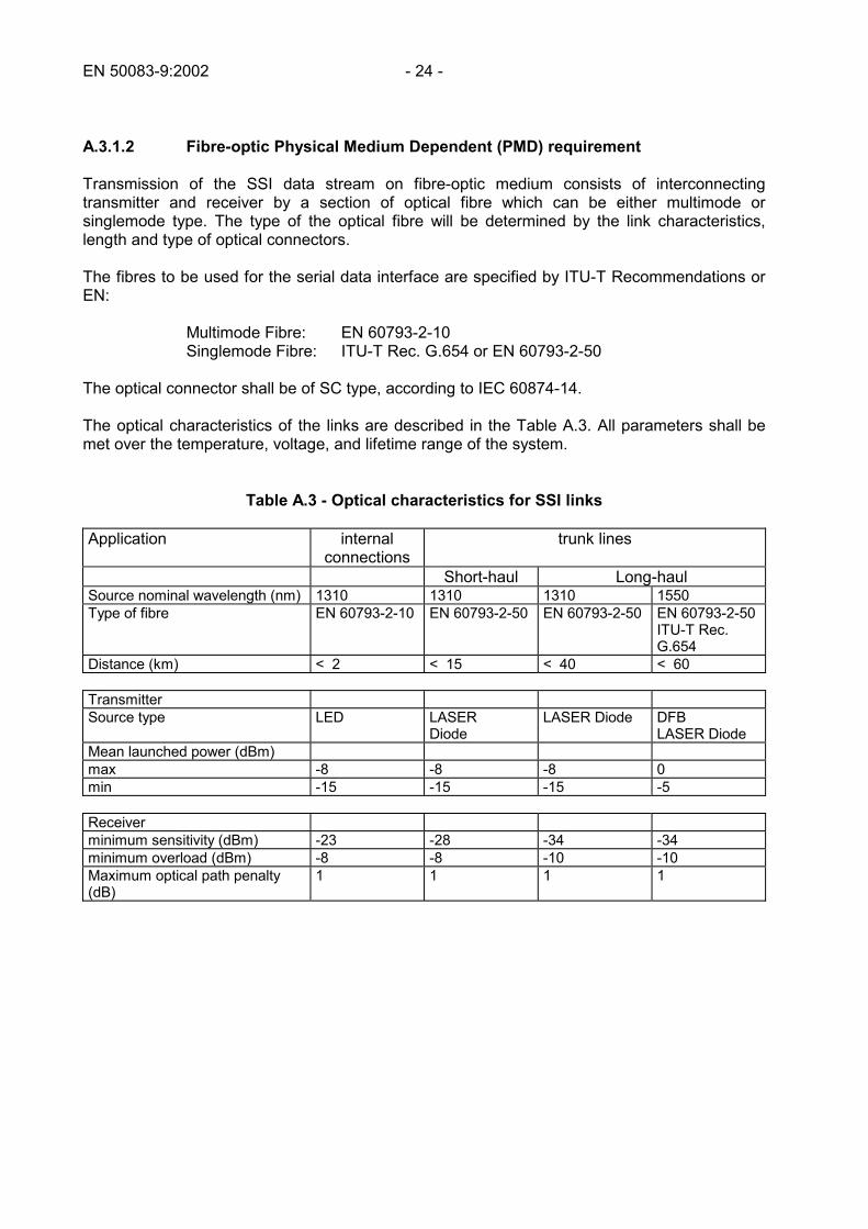
A.3.1.2 Fibre-optic Physical Medium Dependent (PMD) requirement Transmission of the SSI data stream on fibre-optic medium consists of interconnecting transmitter and receiver by a section of optical fibre which can be either multimode or singlemode type. The type of the optical fibre will be determined by the link characteristics, length and type of optical connectors. The fibres to be used for the serial data interface are specified by ITU-T Recommendations or EN:
Multimode Fibre: EN 60793-2-10 Singlemode Fibre: ITU-T Rec. G.654 or EN 60793-2-50
The optical connector shall be of SC type, according to IEC 60874-14. The optical characteristics of the links are described in the Table A.3. All parameters shall be met over the temperature, voltage, and lifetime range of the system.
Table A.3 - Optical characteristics for SSI links Application internal
connections trunk lines
Short-haul Long-haul Source nominal wavelength (nm) 1310 1310 1310 1550 Type of fibre EN 60793-2-10 EN 60793-2-50 EN 60793-2-50 EN 60793-2-50
ITU-T Rec. G.654
Distance (km) < 2 < 15 < 40 < 60 Transmitter Source type LED LASER
Diode LASER Diode DFB
LASER Diode Mean launched power (dBm) max -8 -8 -8 0 min -15 -15 -15 -5 Receiver minimum sensitivity (dBm) -23 -28 -34 -34 minimum overload (dBm) -8 -8 -10 -10 Maximum optical path penalty (dB)
1 1 1 1
- 25 - EN 50083-9: 2002 A.3.2 Layer-1: Data encoding The SSI Layer-1 deals with encoding/decoding aspects which are independent of the transmission medium characteristics. Furthermore, this first layer performs the recognition of the three different transmission formats (see Figures 6, 7 and 8) in order to allow a fully transparent serialisation / deserialisation. Layer-1 operations consist of: - distinguishing the three transmission formats; - parallel to serial conversion of the 8-bit byte with the MSB transmitted first; - Biphase Mark coding of the serial signal in the transmitter. The inverse operations are performed in the receiver. Distinction between the three transmission formats on the serial link is performed as follows: - the transmission format with 188 byte packets (Figure 6) is characterized by a
synchronization byte 47H, the periodicity of which is 188 bytes; - the transmission format with 204 byte packets with 16 dummy bytes (Figure 7) is
characterized by a synchronization byte 47H, the periodicity of which is 204 bytes; - the transmission format of packets of 204 bytes with valid extra bytes (Figure 8) is
characterized by an inverted synchronization byte (B8H) the periodicity of which is 204 bytes.
Line coding A Biphase Mark Code shall be used. Figure A.6a describes the rules of Biphase Mark coding whereas Figure A.6b illustrates that the required medium bandwidth is twice the bandwidth required by NRZ coding. The encoding rules are as follows: - a transition always occurs at the beginning of the bit whatever its value is (0 or 1). - for logical 1, a transition occurs in the middle of the bit - for logical 0, there is no transition on the middle of the bit.
EN 50083-9:2002 - 26 -
CLOCK
NRZDATA
DATABIPHASE
these 2 levels are depending on initial condition
Figure A.6a - Biphase Mark coding scheme
0 0,5 1 1,5 2 2,5 3 3,5 4-40
-35
-30
-25
-20
-15
-10
-5
0
dB
D= (f T)f .
f T.
Figure A.6b - Spectral density of Biphase Mark Code (T is the bit duration of NRZ data)
Figure A.6 - Biphase Mark encoding
Byte synchronization The byte synchronization process in the receiving equipment has to take into account the two possible packet formats, i.e. the 188 byte packet format and the 204 byte packet format. The packet synchronization byte (47H or B8H) is used as a byte alignment pattern which serves for initializing the serial to parallel conversion. The occurrence of the synchronization byte (188 bytes or 204 bytes) and the value of the synchronization byte (47H or B8H) are used to restore the DVALID signal and the PSYNC signal.
- 27 - EN 50083-9: 2002 If the received transmission format is 204 byte packet with valid extra bytes as indicated in Figure 8 the synchronisation byte (B8H) must be inverted in order to recover the original synchronisation byte (47H) of the TS packet format to be delivered to layer-2. NOTE In order to prevent possible synchronisation errors, it is recommended that consecutive bytes 47H do not occur within the 188 byte or 204 byte data packet. Clock recovery In the receiver the clock recovery circuit extracts the transport clock directly from the encoded data stream. The clock corresponds directly to the user data rate. Bit-Error-Rate (BER) requirement The BER shall be less than one part in 1013, as measured where data passes from Layer-1 to Layer-2. That is, BER shall be measured where data emerge from the Biphase Mark decoder. A.3.3 Layer-2: Transport protocol The SSI Layer-2 uses the MPEG-2 Transport Stream as defined in EN ISO/IEC 13818-1 as its basic message unit. The MPEG-2 Transport Packet synchronization byte (47H) is included in this Layer-2 packet definition to allow receive equipment to achieve synchronization. The Transport Packets shall be presented to Layer-2 either as contiguous 188 byte packets, or separated by 16 dummy bytes, or contiguous Reed Solomon encoded 204 byte packets.
EN 50083-9:2002 - 28 -
Annex B (normative)
Asynchronous Serial Interface (ASI)
This annex describes a system for a serial, encoded transmission of different data rates with a constant transmission rate, based on a layered structure of MPEG Transport Packets according to EN ISO/IEC 13818-1 as a top layer (Layer-2), and a pair of bottom layers (Layer- 1 and Layer-0) based upon the Fibre Channel (FC) described in the ISO/IEC 14165-111 „Information technology - Fibre Channel - Part 111: Physical and signalling interface (FC-PH)“. Layer-1 and Layer-0 are based upon a subset of Fibre Channel Levels FC-1 and FC-0 . Transport Streams from different sources may have different data rates. The use of a constant transmission rate permits a constant receiver clock. To restore the original clock rate, a PLL circuit can be used. Annex E gives some proposals for how such a circuit can be designed. The input of the required transmission facility accepts MPEG-2 bytes and the output delivers MPEG-2 bytes. While the Fibre-Channel (FC) supports single mode fibre, multi-mode fibre, coaxial cable and twisted pair media interfaces, this standard defines only two distinct forms of interfaces: coaxial cable and multi-mode fibre-optical cable using LED emitters. Instead of a transmission rate of 265,625 Mbit/s, as required in the ISO/IEC standard, in this document the transmission rate is 270,000 Mbit/s. B.1 ASI transmission system overview Figures B.1 and B.2 represent the primary components of the ASI transmission method over copper coaxial cable and fibre-optic cable, respectively.
Figure B.1 - Coaxial cable-based asynchronous serial transmission link (ASI type)
Sync Byte (FC Comma)
Insertion
Sync Byte (FC Comma)
Deletion
Clock/Data Recovery &
Serial/ParallelConversion
Coupling/ Impedance Matching
8B/10B Decoding
Amplifier/ Buffer
Connector
Parallel/SerialConversion
Coupling/ Impedance Matching
8B/10B Coding
Amplifier/ Buffer
Connector
Coaxial Cable
Packet-Synchronous MPEG2 TS
Packet- Synchronous MPEG-2 TS
Layer-1 Layer-0Layer-2
- 29 - EN 50083-9: 2002
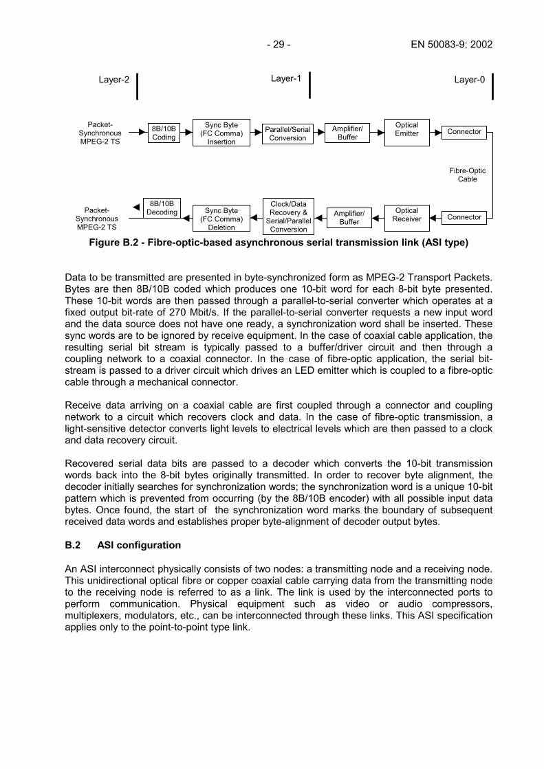
Figure B.2 - Fibre-optic-based asynchronous serial transmission link (ASI type) Data to be transmitted are presented in byte-synchronized form as MPEG-2 Transport Packets. Bytes are then 8B/10B coded which produces one 10-bit word for each 8-bit byte presented. These 10-bit words are then passed through a parallel-to-serial converter which operates at a fixed output bit-rate of 270 Mbit/s. If the parallel-to-serial converter requests a new input word and the data source does not have one ready, a synchronization word shall be inserted. These sync words are to be ignored by receive equipment. In the case of coaxial cable application, the resulting serial bit stream is typically passed to a buffer/driver circuit and then through a coupling network to a coaxial connector. In the case of fibre-optic application, the serial bit-stream is passed to a driver circuit which drives an LED emitter which is coupled to a fibre-optic cable through a mechanical connector. Receive data arriving on a coaxial cable are first coupled through a connector and coupling network to a circuit which recovers clock and data. In the case of fibre-optic transmission, a light-sensitive detector converts light levels to electrical levels which are then passed to a clock and data recovery circuit. Recovered serial data bits are passed to a decoder which converts the 10-bit transmission words back into the 8-bit bytes originally transmitted. In order to recover byte alignment, the decoder initially searches for synchronization words; the synchronization word is a unique 10-bit pattern which is prevented from occurring (by the 8B/10B encoder) with all possible input data bytes. Once found, the start of the synchronization word marks the boundary of subsequent received data words and establishes proper byte-alignment of decoder output bytes. B.2 ASI configuration An ASI interconnect physically consists of two nodes: a transmitting node and a receiving node. This unidirectional optical fibre or copper coaxial cable carrying data from the transmitting node to the receiving node is referred to as a link. The link is used by the interconnected ports to perform communication. Physical equipment such as video or audio compressors, multiplexers, modulators, etc., can be interconnected through these links. This ASI specification applies only to the point-to-point type link.
Sync Byte (FC Comma)
Insertion
Sync Byte (FC Comma)
Deletion
Clock/Data Recovery &
Serial/ParallelConversion
Optical Receiver
8B/10B Decoding Amplifier/
Buffer Connector
Parallel/SerialConversion
Optical Emitter 8B/10B
Coding Amplifier/
Buffer Connector
Fibre-OpticCable
Packet-Synchronous MPEG-2 TS
Packet-Synchronous MPEG-2 TS
Layer-1 Layer-0Layer-2
EN 50083-9:2002 - 30 - B.3 ASI protocol architecture description The ASI protocol is divided into three architectural layers for purposes of development of the standard: Layer-0, Layer-1, and Layer-2. B.3.1 Layer-0: Physical requirements The physical layer defines the transmission media, the drivers and receivers, and the transmission speeds. The physical interface provides for both LED-driven multimode fibre and copper coaxial cable. The base speed is defined as 270 Mbit/s (transmission channel speed). The basic unit of Layer-0 is the link. The points where conformance is required are shown as point S and R in the Figure B.3.
Figure B.3 - Serial link Layer-0 reference points In coaxial applications, jitter is specified in the traditional manner of random and data dependent jitter and duty cycle distortion. In LED-driven fibre based applications, jitter is specified in terms of Random Jitter (RJ) and Deterministic Jitter (DJ). Deterministic Jitter is the sum of data dependent jitter and duty cycle distortion. The DJ is due to the timing distortions caused by normal circuit effects in the transmission system. It comprises of propagation delay difference between the rising and falling edge of a signal and interaction of limited bandwidth of the transmission components and the symbol sequence. The RJ is due to the thermal noise in the system and usually modelled as a Gaussian process. Line rates and bit timing The encoded line rate with the 8B/10B block code is 270 Mbit/s which results in a media transmission rate of 270 MBaud. At the transmitter the serialisation is done using a fixed oscillator to establish this 270 MBaud rate from which a phase-locked byte clock is derived and used to shift in parallel bytes. Receivers recover the serial transmission clock generally by the use of a phase-locked-loop (PLL) oscillator locked to bit transitions of the incoming data stream. A phase-locked byte clock is derived from this recovered serial bit clock and is used to shift parallel bytes out to Layer-1 processing elements. It is required that the encoded line rate shall be 270 MBaud ± 100 ppm. Receiver timing acquisition A receiver shall first acquire bit synchronization, before attempting to align received bytes. This time is measured from receipt of a valid input to the time the receiver is synchronized to the bit stream and delivering valid re-timed data within the BER objective of the system. It is required that bit synchronization shall occur in not more than 1 ms.
Receiver (Rx)
Transmitter (Tx)
Cable or Fibre LinkS R
Connector Plug
- 31 - EN 50083-9: 2002 B.3.1.1 Electrical medium characteristics The nominal cable impedance shall be 75 Ω. Electrical medium connector The required connector shall have mechanical characteristics conforming to the BNC type. NOTE Due to its higher mechanical stability a 50 Ω BNC type connector according to IEC 60169-8 is recommended. The electrical characteristics of the connector shall permit it to be used over the frequency range of the specified interface. Electrical characteristics The parameters shall be met over the temperature, voltage and lifetime range of the system. Electrical measurements shall be made with the interface terminated with the connector specified above into 75 Ω resistive termination. Full electrical details are provided in Table B.1.
Table B.1 - Electrical characteristic specifications for ASI link
Transmitter output characteristics Units Output voltage (p-p) mV 800 ± 10% Deterministic Jitter (DJ) (p-p) % 10 Random Jitter (RJ) (p-p) % 8 Return loss dB under consideration Max. rise/fall time (20-80%) ns 1,2
Receiver input characteristics Units Min. sensitivity (D21.5 idle pattern) mV 200 Max. input voltage (p-p) mV 880 s11 (range: 0,1 to 1,0 x bit rate) dB -17 Min. discrete connector return loss (5 MHz - 270 MHz)
dB -15
The interface shall be coupled to the coaxial system via a transformer. As measured according to the diagramme in Figure B.4, the eye opening provided by the transmitter shall be within the mask depicted in Figure B.5.
Figure B.4 - Coaxial transmitter test circuit
TX
TY
+75Ω_
TransmitNetwork
EN 50083-9:2002 - 32 -
0.15 0.35 0.65 0.85
0.3
0.5
0.7
1.0
normalizedamplitude
normalizedtime
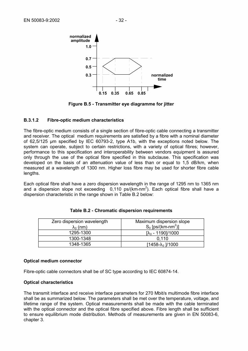
Figure B.5 - Transmitter eye diagramme for jitter B.3.1.2 Fibre-optic medium characteristics The fibre-optic medium consists of a single section of fibre-optic cable connecting a transmitter and receiver. The optical medium requirements are satisfied by a fibre with a nominal diameter of 62,5/125 µm specified by IEC 60793-2, type A1b, with the exceptions noted below. The system can operate, subject to certain restrictions, with a variety of optical fibres; however, performance to this specification and interoperability between vendors equipment is assured only through the use of the optical fibre specified in this subclause. This specification was developed on the basis of an attenuation value of less than or equal to 1,5 dB/km, when measured at a wavelength of 1300 nm. Higher loss fibre may be used for shorter fibre cable lengths. Each optical fibre shall have a zero dispersion wavelength in the range of 1295 nm to 1365 nm and a dispersion slope not exceeding 0,110 ps/(km*nm2). Each optical fibre shall have a dispersion characteristic in the range shown in Table B.2 below:
Optical medium connector Fibre-optic cable connectors shall be of SC type according to IEC 60874-14. Optical characteristics The transmit interface and receive interface parameters for 270 Mbit/s multimode fibre interface shall be as summarized below. The parameters shall be met over the temperature, voltage, and lifetime range of the system. Optical measurements shall be made with the cable terminated with the optical connector and the optical fibre specified above. Fibre length shall be sufficient to ensure equilibrium mode distribution. Methods of measurements are given in EN 50083-6, chapter 3.
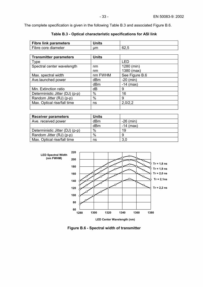
- 33 - EN 50083-9: 2002 The complete specification is given in the following Table B.3 and associated Figure B.6.
Table B.3 - Optical characteristic specifications for ASI link
Fibre link parameters Units Fibre core diameter µm 62,5
Transmitter parameters Units Type LED Spectral center wavelength nm
nm 1280 (min) 1380 (max)
Max. spectral width nm FWHM See Figure B.6 Ave.launched power dBm -20 (min) dBm -14 (max) Min. Extinction ratio dB 9 Deterministic Jitter (DJ) (p-p) % 16 Random Jitter (RJ) (p-p) % 9 Max. Optical rise/fall time ns 2,0/2,2
Receiver parameters Units Ave. received power dBm -26 (min) dBm -14 (max) Deterministic Jitter (DJ) (p-p) % 19 Random Jitter (RJ) (p-p) % 9 Max. Optical rise/fall time ns 3,0
1280 1300 1320 1340 1360 138060
80
100
120
140
160
180
200
220LED Spectral Width
(nm FWHM)
LED Center Wavelength (nm)
Tr = 2,2 ns
Tr = 1,8 ns
Tr = 1,9 nsTr = 2,0 ns
Tr = 2,1ns
Figure B.6 - Spectral width of transmitter
EN 50083-9:2002 - 34 - B.3.2 Layer-1: Data encoding The ASI transmission protocol includes serial encoding rules, special characters, and error control. It uses a DC balanced 8B/10B transmission code. The code maps each 8-bit data byte into a 10-bit code with the following properties: a run length of 4 bits or less and minimal DC offset. This code provides error checking through both invalid transmission code points and the notion of 'running' disparity. Special characters are defined as extra code points beyond the need to encode a byte of data. One in particular, the comma character (K28.5 in the Tables of annex C) is used to establish byte synchronization in the ASI transmission link. Coding requirements The ASI transmission Layer-1 deals with encoding/decoding aspects which are independent of the transmission medium characteristics. At Layer-1, 8B/10B transmission coding is employed which provides for both a self checking capability and byte synchronization of the link. The 10B transmission code is defined in terms of "disparity", i.e. the difference in the number of "1" bits and "0" bits in the transmitted serial data stream. It is through the disparity characteristics of the code that DC balance is maintained. Each 8B code point has two entries in the 10B code point map corresponding to the positive and negative disparity representation for that 8B code point. The transmitter is required to maintain the running disparity of the transmitted serial bit stream within +/-1 of a neutral point by selection of the appropriate positive or negative disparity representation of the 10B code to be transmitted. The receiver will check the incoming bit stream for proper running disparity and invalid 10B code points to ensure byte level data integrity. Line coding The 8B/10B transmission code specified in the Fibre Channel document [3] shall be the encoding method utilized in ASI interface Layer-1. Annex C is a reproduction of the 8B/10B coding Table from that standard and a brief description of the coding process. NOTE The ASI coding is not invariant to logical inversion of the transmitted bits. Therefore, to ensure correct operation, care must be taken that equipment interface circuitry of the non-inverting type is used. Byte synchronization The byte alignment synchronization pattern shall be the K28.5 code of the 8B/10B code. The receiver shall present a properly aligned byte stream after the receipt of two K28.5 special characters aligned on the same byte boundary within a 5 byte window. The first byte received after the second K28.5 shall have valid byte alignment. Bit-Error-Rate (BER) performance The BER shall be less than one part in 1013, as measured where data passes from Layer-1 to Layer-2. That is, BER shall be measured where bytes emerge from the 8B/10B decoder. Packet synchronization At least two synchronization code words (K28.5) shall immediately precede every Layer-2 Transport Packet.
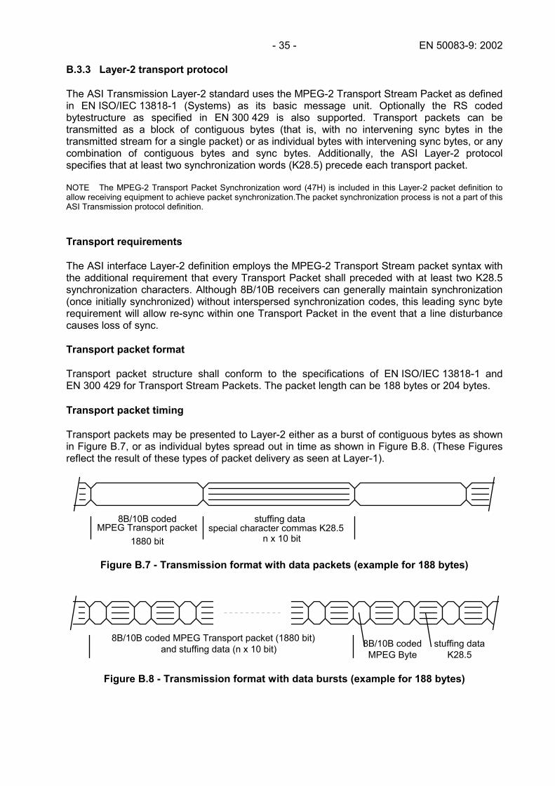
- 35 - EN 50083-9: 2002 B.3.3 Layer-2 transport protocol The ASI Transmission Layer-2 standard uses the MPEG-2 Transport Stream Packet as defined in EN ISO/IEC 13818-1 (Systems) as its basic message unit. Optionally the RS coded bytestructure as specified in EN 300 429 is also supported. Transport packets can be transmitted as a block of contiguous bytes (that is, with no intervening sync bytes in the transmitted stream for a single packet) or as individual bytes with intervening sync bytes, or any combination of contiguous bytes and sync bytes. Additionally, the ASI Layer-2 protocol specifies that at least two synchronization words (K28.5) precede each transport packet. NOTE The MPEG-2 Transport Packet Synchronization word (47H) is included in this Layer-2 packet definition to allow receiving equipment to achieve packet synchronization.The packet synchronization process is not a part of this ASI Transmission protocol definition. Transport requirements The ASI interface Layer-2 definition employs the MPEG-2 Transport Stream packet syntax with the additional requirement that every Transport Packet shall preceded with at least two K28.5 synchronization characters. Although 8B/10B receivers can generally maintain synchronization (once initially synchronized) without interspersed synchronization codes, this leading sync byte requirement will allow re-sync within one Transport Packet in the event that a line disturbance causes loss of sync. Transport packet format Transport packet structure shall conform to the specifications of EN ISO/IEC 13818-1 and EN 300 429 for Transport Stream Packets. The packet length can be 188 bytes or 204 bytes. Transport packet timing Transport packets may be presented to Layer-2 either as a burst of contiguous bytes as shown in Figure B.7, or as individual bytes spread out in time as shown in Figure B.8. (These Figures reflect the result of these types of packet delivery as seen at Layer-1).
8B/10B codedMPEG Transport packet
stuffing dataspecial character commas K28.5
1880 bit n x 10 bit
Figure B.7 - Transmission format with data packets (example for 188 bytes)
MPEG Byte8B/10B coded stuffing data
K28.5and stuffing data (n x 10 bit)8B/10B coded MPEG Transport packet (1880 bit)
Figure B.8 - Transmission format with data bursts (example for 188 bytes)
EN 50083-9:2002 - 36 -
Annex C (informative)
8B/10B tables
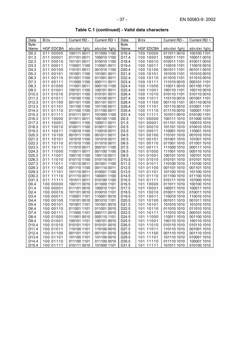
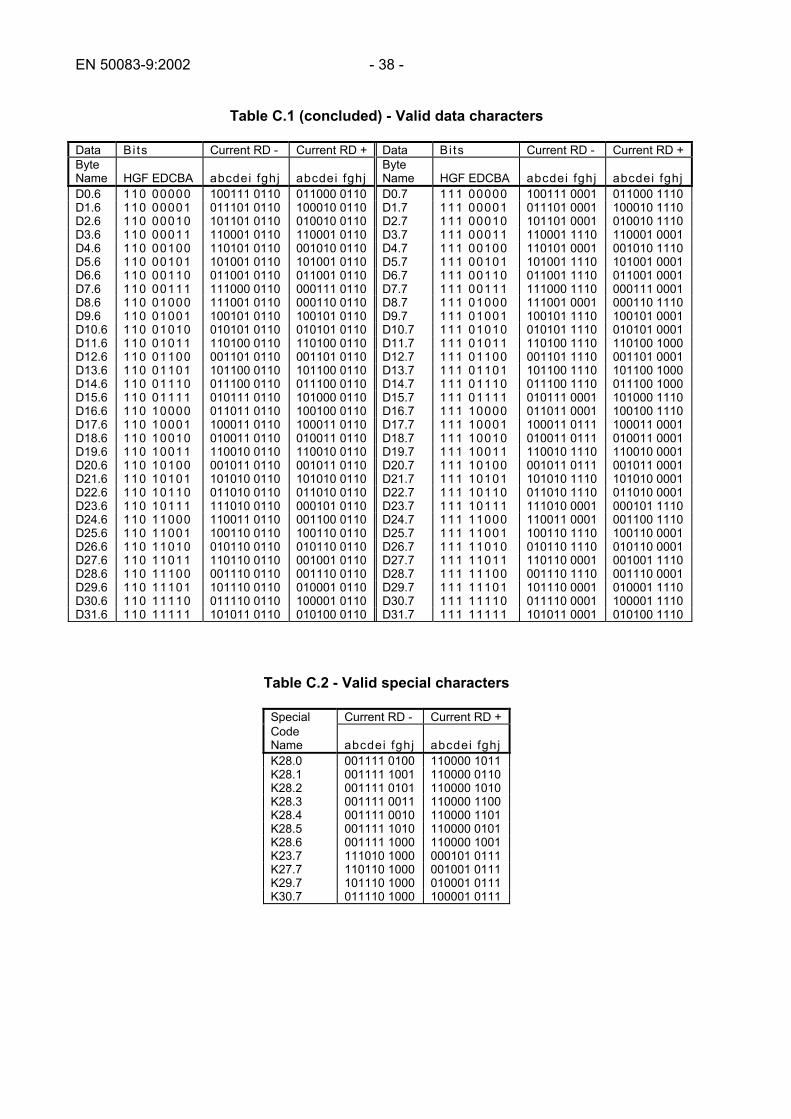
Table C.1 - Valid data characters
Data Bi ts Current RD - Current RD + Data Bi ts Current RD - Current RD + Byte Name
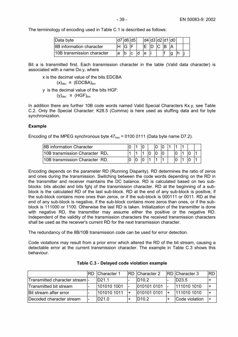
- 39 - EN 50083-9: 2002 The terminology of encoding used in Table C.1 is described as follows:
Data byte d7 d6 d5 d4 d3 d2 d1 d0 8B information character H G F E D C B A 10B transmission character a b c d e i f g h j
Bit a is transmitted first. Each transmission character in the table (Valid data character) is associated with a name Dx.y, where x is the decimal value of the bits EDCBA (x)dec ≡ (EDCBA)bin y is the decimal value of the bits HGF: (y)dec ≡ (HGF)bin In addition there are further 10B code words named Valid Special Characters Kx.y, see Table C.2. Only the Special Character: K28.5 (Comma) is here used as stuffing data and for byte synchronization. Example Encoding of the MPEG synchronous byte 47hex = 0100 0111 (Data byte name D7.2).
8B information Character 0 1 0 0 0 1 1 1 10B transmission Character RD+ 1 1 1 0 0 0 0 1 0 1 10B transmission Character RD- 0 0 0 1 1 1 0 1 0 1
Encoding depends on the parameter RD (Running Disparity). RD determines the ratio of zeros and ones during the transmission. Switching between the code words depending on the RD in the transmitter and receiver maintains the DC balance. RD is calculated based on two sub-blocks: bits abcdei and bits fghj of the transmission character. RD at the beginning of a sub-block is the calculated RD of the last sub-block. RD at the end of any sub-block is positive, if the sub-block contains more ones than zeros, or if the sub-block is 000111 or 0011. RD at the end of any sub-block is negative, if the sub-block contains more zeros than ones, or if the sub-block is 111000 or 1100. Otherwise the last RD is taken. Initialization of the transmitter is done with negative RD, the transmitter may assume either the positive or the negative RD. Independent of the validity of the transmission characters the received transmission characters shall be used as the receiver's current RD for the next transmission character. The redundancy of the 8B/10B transmission code can be used for error detection. Code violations may result from a prior error which altered the RD of the bit stream, causing a detectable error at the current transmission character. The example in Table C.3 shows this behaviour.
Table C.3 - Delayed code violation example RD Character 1 RD Character 2 RD Character 3 RDTransmitted character stream - D21.1 - D10.2 - D23.5 + Transmitted bit stream - 101010 1001 - 010101 0101 - 111010 1010 + Bit stream after error - 101010 1011 + 010101 0101 + 111010 1010 + Decoded character stream - D21.0 + D10.2 + Code violation +
EN 50083-9:2002 - 40 -
Data (0-7)
Clock
DVALID
Annex D (informative)
Implementation guidelines and clock recovery from the
Synchronous Serial Interface (SSI) D.1 Example of implementation of the SSI interface Hardware implementation of the proposed SSI interface was undertaken in order to validate the serial transmission in a real MPEG-2 chain including TS multiplexer, QPSK modulator/demodulator, QAM modulator/demodulator. It consists of two adapter modules: - an emitting module which transforms the parallel interface, such as described in 4.1 into
the serial mode; - a receiving module which performs the reverse function in recovering the Transport
Packets conforming to the parallel interface.
Figure D.1 - Connection of the adapter modules D.2 Emitting module The main functions are: - The parallel to serial conversion - The generation of the serial clock by a multiplication by 8 of the parallel clock. - Biphase-Mark encoding . As an example, using a Manchester Biphase-Mark encoder. - LED driver for optical transmission - Cable driver for coaxial transmission
coaxial or fibre
system 1
1 Clock
DVALID PSYNC
Data (0-7) 8
1
TX parallel-serial adapter 1
1
PSYNC
8
1
serial-parallel adapter
RX
- 41 - EN 50083-9: 2002
ParallelClock reference
Parallel/Serial
Conversion
Biphase
encoder
Amplifier/Buffer
Coupling/Impedancematching
LEDoutput
SERIALINTERFACE
PARALLELINTERFACE
Data (0-7)
outputCoaxial
1:8
progammableserial clockgenerator
DVALID
PSYNC
Figure D.2 - Example of implementation of an emitting module D.3 Receiving module The byte synchronization process in the receiving equipment has to take into account the two possible packet formats, i.e. the 188 byte-packet format and the 204 byte-packet format. An automatic byte synchronization was performed as follows: - a first attempt of synchronization can be done on the hypothesis of 188 byte-packet
format; - if the first attempt is unsuccessful, the synchronization is done on the 204 byte-packet
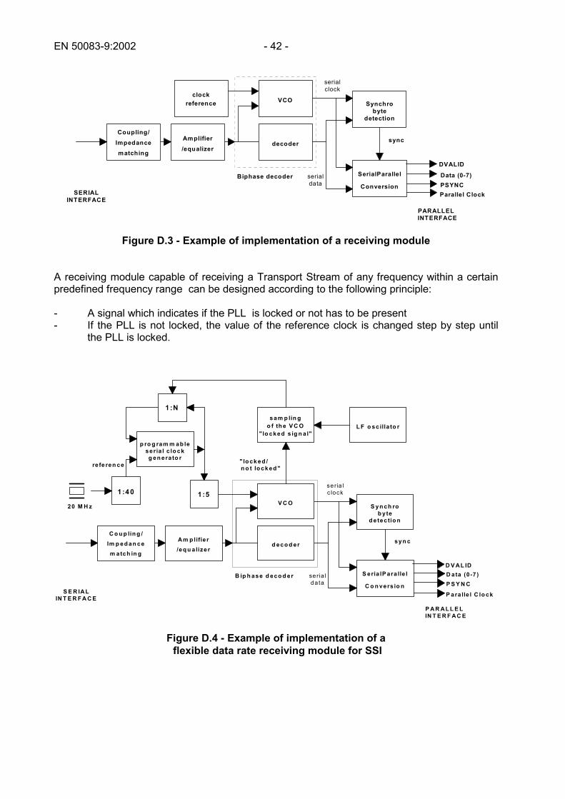
format. The main functions are: - Cable equalizer for coaxial reception - Optical receiver for optical reception - Clock recovering and Biphase Mark decoding . As an example, using a Manchester Biphase Mark decoder. - Byte synchronization and deserialisation
EN 50083-9:2002 - 42 -
SERIALINTERFACE
PARALLELINTERFACE
Data (0-7)
Parallel ClockPSYNC
SerialParallel
Conversion
Amplifier/equalizer
Coupling/Impedancematching
Synchrobyte
detection
sync
serialdata
VCO
decoder
Biphase decoder
clockreference
serialclock
DVALID
Figure D.3 - Example of implementation of a receiving module A receiving module capable of receiving a Transport Stream of any frequency within a certain predefined frequency range can be designed according to the following principle: - A signal which indicates if the PLL is locked or not has to be present - If the PLL is not locked, the value of the reference clock is changed step by step until
the PLL is locked.
S E R IALIN T E R F A C E
P AR AL L E LIN T E R F AC E
D ata (0 -7 )
P ara lle l C lo ck
P S Y N CS eria lP ara lle l
C o n vers io n
Am p lifie r/eq u a lizer
C o u p lin g /Im p ed an cem atch in g
S yn ch rob yte
d etectio n
syn c
seria lda ta
V C O
d eco d er
B ip h ase d eco d er
seria lc lock1 :51 :4 0
1 :Nsam p lin g
o f th e V C O"lo cked s ig n a l"
L F o sc illa to r
20 M H z
refe ren ce
p ro g ram m ab leseria l c lo ckg en era to r " lo ck ed /
n o t lo ck ed "
D V AL ID
Figure D.4 - Example of implementation of a flexible data rate receiving module for SSI
- 43 - EN 50083-9: 2002 D.4 Physical media Different physical media can be used : Coaxial cable With the requirements, given in A.3.1.1, the following typical links can be handled: For coaxial cables equivalent to RG 59 BU: a maximum distance of 100 m For coaxial cables equivalent to RG 216 U: a maximum distance of 220 m Optical fibre Multimode or Singlemode: several km, depending on configuration.
EN 50083-9:2002 - 44 -
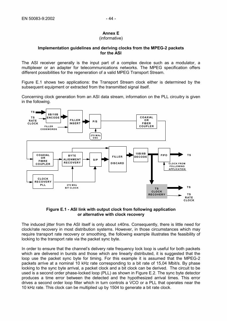
Annex E (informative)
Implementation guidelines and deriving clocks from the MPEG-2 packets
for the ASI The ASI receiver generally is the input part of a complex device such as a modulator, a multiplexer or an adapter for telecommunications networks. The MPEG specification offers different possibilities for the regeneration of a valid MPEG Transport Stream. Figure E.1 shows two applications: the Transport Stream clock either is determined by the subsequent equipment or extracted from the transmitted signal itself. Concerning clock generation from an ASI data stream, information on the PLL circuitry is given in the following.
8B/10BENCODE COAXIAL
FIBERCO UPLER
O R
CO AXIAL
FIBRECO UPLER
O RBYTE
ALIG NMENTRECO VERY
10B/8BDECO DE
CLO CKRECOVERY
PLL
S/P
P/SFILLERINSERT
DISCARD
FILLER
270 M HzO SC
270 M HzBIT CLO CK
TS
TS
TSRATE
CLO CKFILLER
CO DEWO RDS
FIFO
RECO VERYCLO CK
TS TS
CLO CK FRO M
APPLICATIO NFO LLO WING
TSRATE
CLO CK
Figure E.1 - ASI link with output clock from following application or alternative with clock recovery
The induced jitter from the ASI itself is only about ±40ns. Consequently, there is little need for clock/rate recovery in most distribution systems. However, in those circumstances which may require transport rate recovery or smoothing, the following example illustrates the feasibility of locking to the transport rate via the packet sync byte. In order to ensure that the channel’s delivery rate frequency lock loop is useful for both packets which are delivered in bursts and those which are linearly distributed, it is suggested that the loop use the packet sync byte for timing. For this example it is assumed that the MPEG-2 packets arrive at a nominal 10 kHz rate corresponding to a bit rate of 15,04 Mbit/s. By phase locking to the sync byte arrival, a packet clock and a bit clock can be derived. The circuit to be used is a second order phase-locked loop (PLL) as shown in Figure E.2. The sync byte detector produces a time error between the detected and the hypothesized arrival times. This error drives a second order loop filter which in turn controls a VCO or a PLL that operates near the 10 kHz rate. This clock can be multiplied up by 1504 to generate a bit rate clock.
- 45 - EN 50083-9: 2002
SYNC BYTE &TIME
ERRORDETECTOR
SECOND ORDERLOOP FILTER
10 kHz VCO
15.04 MHz VCO
ERROR
CONTROL
MPEG-2PACKETS
FIFO forTRANSPORT
RATE CONTROLFREQUENCYACQUISITION
& JITTER
Figure E.2 - Phase Locked Loop for clock generation It is also assumed in this simplified example that the transport rate shall be known in order to set the loop multiplier due to the wide range of rates which shall be tracked. Of course, MPEG clock timing constraints are also assumed. A FIFO buffer is included in this example in order to • provide a smoothing buffer for the output rate control mechanism; • provide a clock acquisition buffer to account for the initial rate differential between input
and output as the PLL adapts to the changing transport rates with possibly different (up to 60ppm) rate clocks;
• buffer the packet jitter which may be introduced by the interface or attached equipment (likely to be very small).
Table E.1 contains a mathematical analysis and simulation of the difference equations comprising a digital implementation of the circuit in Figure E.2. The assumptions are that the arrival rate is 10 kHz with a ±50 µs uniform jitter (θn). The loop constants K1 and K2 are chosen to make the damping factor 0,707 and the loop bandwidth 52,5 Hz, assuming a 10 kHz sample rate. The variable ACCTn is the accumulator in the loop filter, and it converges to the time interval between arriving sync bytes. Consequently, its inverse is the rate at which sync bytes arrive. The first curve shows this rate converging to 10 kHz after about 700 samples (0,07 s). The frequency accuracy is shown by computing the mean (Amean) and standard deviation (Asd) of this inverse. The next set of calculations show the clock accuracy in seconds with the standard deviation being about 19 ns. The deviation, or jitter, may be traded for acquisition time, as an MPEG-2 decoder suppose more than 19 ns of apparent packet jitter. Table E.2 shows a mathematical analysis and simulation for the circuit of Figure E.2 operating with a delivery rate that jitters at ± 2 ms. Note that the loop still acquires synchronization in about 700 samples, or 0,07 s. The accuracy of the derived clock is depicted by Amean and Asd for the frequency, and Tmean and Tsd for the time. The standard deviation of the time is now 765 ns, or about 40 times the results of Table E.1. This is still very small relative to the currently suggested real time jitter constraint for MPEG-2 decoders.
Table E.2 - Analysis of 10 kHz clock generating loop, ± 2 ms jitter
EN 50083-9:2002 - 48 -
Annex F (informative)
Guidelines for the implementation and usage of the
DVB Asynchronous Serial Interface F.1 Introduction The DVB Asynchronous Serial Interface (ASI) is a very popular standard interface for conveying MPEG-2 transport streams between professional equipment. However, there are concerns over interoperability in the market place, based on system integrators’ experiences with available equipment from multiple suppliers. This note is intended to explain some of the causes of problems and to offer guidelines to ASI implementers that will encourage maximum interoperability. F.2 Scope The present document addresses interoperability issues specific to ASI data transmission links, and explicitly is not concerned with general MPEG-2 interoperability issues. An example of an ASI interoperability problem is where equipment receiving an ASI data stream occasionally drops out of lock, or never achieves lock at all. An example of a problem not addressed by these guidelines is where the video and audio on the output of a decoder have poor clock stability, because of PCR clock recovery problems at some point in the end-to-end equipment chain, for example resulting in LF wander in a regenerated PAL/NTSC subcarrier. The present document contains a clause providing a description of the design issues confronting ASI equipment designers. The present document also contains a recommendation clause, which provides simple measures to improve interoperability between ASI equipment. There may be situations where systems will work outside these recommendations, depending on precise system and equipment implementation. F.3 ASI transmission links The ASI is a uni-directional transmission link to transfer data between professional digital video equipment. Figure F.1 presents an abstract model of an ASI transmission link. The model represents signals at the Layer 1/Layer 0 interface of Figure B.1.
R
rx-clk
T
tx-clk
VariableDelay
ASI-Link
Figure F.1 - Abstract ASI transmission model
TB RB
- 49 - EN 50083-9: 2002 The diagram contains an ASI transmission node, where data are held in a transmission buffer TB. Data are read from this buffer at a constant rate determined by the transmission clock (tx-clk). This generates an isochronous data stream. One should keep in mind that the ASI is asynchronous. This gives implementers the freedom to deviate from isochronous data delivery. The diagram models this explicitly by including a “Variable Delay” function. The modified stream is transported over the ASI link to arrive at the receiver buffer RB. Data are removed from this buffer at a constant rate, determined by the receiver clock (rx-clk). The abstract ASI delivery model is used to make sure that the isochronous output stream from the receiver buffer is similar to the isochronous input stream to the variable delay function. A design issue in this transmission model is that bytes need to be removed from the receiver buffer at a high enough data rate. To achieve this, the receiver clock frequency needs to be equal to or greater than the transmission clock frequency. If this is not the case, the receiver buffer will overflow. The present document assumes that the receiver clock is linked to the transmission clock, but is silent about how to achieve this in practice. When the receiver clock is linked to the transmission clock, the remaining design issue is to remove any aperiodicity introduced in the isochronous data stream. On the ASI link, the bytes can be displaced in time with respect to their isochronous position. This displacement can occur for a variety of reasons, e.g. technical convenience at the generating end of the link. The ASI specification allows for unlimited time displacement of data bytes. To improve interoperability, ASI implementations need to be subject to certain restrictions on the data transmission. The variable delay block in the diagram models the asynchronous transmission characteristics of the ASI. The aperiodicity can be expressed as a short-term change in the transport rate. A good starting point is the definition of data rate from the DVB Measurement Group that is contained in ETR 290 rev.1. In this DVB specification, the data rate is averaged over a fixed time gate (called “window”). Each window contains a fixed number of N “time slices”. For the time slice number k, the notation Dk represents the number of bytes transferred in that period of time. The average data rate (in bytes per second) is then given by the formula:
T
DrateASI
Nn
nnk
k
∑−=
=−
=
1
0_ (bytes/second)
where N is the integer number of time slices in the time gate window, T is the duration of the time gate window. After each measurement the time gate window is shifted by one time slice unit of time, denoted by τ = T/N. The rate specification permits different values for N and T. For this analysis, it is assumed that the transmission clock equals the average rate expressed by the formula. As the actual rate may deviate from the average, we introduce the peak rate as the highest rate found in the N time slices. The highest rate then fills the receiver buffer more rapidly than the average rate at which data is removed from the buffer. A temporary higher rate is followed by a temporary lower rate. The combined effect is that the receiver buffer should be empty at the end of the time gate window. An example is shown in Figure F.2.
EN 50083-9:2002 - 50 -
50,150
50,200
50,250
50,300
50,350
50,400
1 11 21 31 41 51 61 71 81 91
-
100
200
300
400
500
600
1 10 19 28 37 46 55 64 73 82 91 100
Figure F.2 - Random aperiodic transport stream rate and buffer utilisation
In this example, a simulated data transport is shown with an average data rate of 50 kbyte/s. The time gate window consists of 100 time slices. The number of bytes transferred in each time slice is shown in the left curve of Figure F.2. The rate varies from 45 kbyte/s to 55 kbyte/s. As the bytes are removed from the ASI receiver buffer at the average rate, the buffer occasionally fills with excess bytes. The number of bytes in the receiver buffer is shown in the right-hand curve. One can see that the buffer occasionally underflows. Both the buffer underflow and the relatively large buffer size should be avoided in practical situations. Another example uses a more well-behaved stream. Here each transport packet is played out with a constant delay between the Sync bytes. The packets are transmitted in a burst with a constant data rate of 8 Mbyte/s. After every packet a small gap is present where no data bytes arrive at the receiver. The data rate is much more constant, and the required receiver buffer also is much lower.
50,150
50,200
50,250
50,300
50,350
50,400
1 11 21 31 41 51 61 71 81 91 101
01020304050607080
1 10 19 28 37 46 55 64 73 82 91 100
Figure F.3 - Deterministic aperiodic transport stream rate and buffer utilisation
Figure F.3 shows that a deterministic aperiodic transport stream has a lower and more predictable buffer utilisation for approximately the same variations in transport rate. The worst case receiver buffer size occurs when all data in the peak rate time slice is transmitted in one burst at the maximum ASI link rate of 27 Mbyte/s. In such a worst case scenario, the peak time slice transports all data and all other time slices carry no data. Both examples shown above highlight the fact that in an ASI design careful consideration needs to be given to the properties of the delay variation of the link. The receiver buffer size, which is required to properly receive the data stream when the transmit and receive rates are linked, should be specified. Hence this measure is used in the recommendations below.
- 51 - EN 50083-9: 2002 F.4 Recommendations It is recommended that equipment manufacturers include the following information on their product data sheets: • for equipment with an ASI input, the size of the ASI receiver buffer in transport packets
that is available to remove ASI transmission aperiodicity should be stated; • for equipment with an ASI output, the minimum ASI receiver buffer size in transport
packets required to remove the ASI transmission aperiodicity it creates should be stated. To maximise equipment interoperability, it is suggested that equipment with an ASI output should be designed to work with equipment with a small ASI receiver buffer. Additionally, an ASI input should be designed with an receiver buffer that accommodates as wide a variety of ASI outputs as possible within appropriate commercial constraints. The aperiodicity of some ASI output streams and the receiver buffer size they require for proper reception is illustrated in the following diagrams. The signals represented in these diagrams occur at the Layer 1/Layer 0 interface of Figure B.1. In the first two diagrams below, the ASI receiver buffer size required would be one MPEG-2 transport packet.
s s s s
1 transport packet period 1 transport packet period 1 transport packet period
s s s s
1 transport packet period 1 transport packet period 1 transport packet period
…. …. ….
sKey: MPEG sync byte MPEG transport byte(s) ASI stuffing byte(s) : K28,5 characters
In the following example, an ASI receiver buffer of three packets would be required to remove the ASI aperiodicity.
s s s s
3 transport packet periods
F.5 Clarifications Note that if the equipment can accept 204-byte transport packets (optional) in addition to 188-byte transport packets (mandatory), then the size of the required buffer in bytes would have to be larger than if only 188-byte transport packets are supported. In some cases, an ASI output may work with an ASI input with a smaller buffer than is specified for the output, however ASI interoperability under these circumstances cannot be guaranteed. In order to establish whether such inputs and outputs will interface to each other correctly, it is necessary to understand precisely the distribution of transport packet bytes and ASI stuffing bytes, and the detailed operation of the equipment. A general solution for this cannot be given.
EN 50083-9:2002 - 52 - Requirements for the ASI input will vary depending on the equipment function, for example a decoder may not need as flexible an ASI input as a remultiplexer.
- 53 - EN 50083-9: 2002
Annex G (informative)
Bibliography
[1] DVB-TM 11 July 1995 Interfaces for CATV/SMATV headends and similar 1449 Rev 1 professional equipment (10th working draft) DVB Project Office c/o European Broadcasting Union 17 A Ancienne Route CH-1218 Grand Saconnex / Geneva Switzerland
[2] EIA/TIA Dec. 1994 Electrical Characteristics of Low Voltage SP 3357 Differential Signaling (LVS) Interface Circuits [3] ANSI 1982 Unified Inch Screw Threads B1.1 (UN and UNR Thread Form) American National Standard (American National Standards Institute 11 W. 42nd Street, New York, New York 10036)