Challenges toward voltage-torque MRAM Shinji Yuasa (AIST, Spintronics Research Center) A magnetic tunnel junction (MTJ) consisting of a thin insulating layer (a tunnel barrier) sandwiched between two ferromagnetic electrodes exhibits the tunnel magnetoresistance (TMR) effect due to spin-dependent electron tunneling. Since the discovery of room-temperature TMR, 1,2) MTJs with an amorphous aluminum oxide (Al–O) tunnel barrier, which exhibit magnetoresistance (MR) ratios of several tens percent, have been studied extensively. In 2004, MR ratios of about 200% were obtained for fully epitaxial MTJs with single-crystal MgO(001) tunnel barrier 3) and textured MTJs with (001)-oriented MgO tunnel barrier 4) . MTJs with a CoFeB/MgO/CoFeB structure were also developed for practical application. 5) In the CoFeB/MgO/CoFeB MTJ, a highly textured MgO(001) barrier layer is grown on an amorphous CoFeB bottom electrode layer. By post-annealing the MTJs, the amorphous CoFeB layers are crystallized in bcc(001) structure due to the solid-phase epitaxial growth from the MgO interfaces 6) . Then, the (001)-textured CoFeB/MgO/CoFeB MTJ exhibit giant MR ratios as well as other practical properties such as low resistance-area (RA) product 7,8) and/or interfacial perpendicular magnetic anisotropy (PMA). 9) Because of the high manufacturability and practical magneto-transport properties, the CoFeB/MgO/CoFeB MTJs are widely used as the read heads of hard disk drives (HDDs), memory cell of non-volatile memory (STT-MRAM) especially with perpendicular magnetization, spin-torque oscillator (STO), and physical random number generator (Spin Dice). 10,11) Although the textured CoFeB/MgO/CoFeB MTJs have been very successful, the properties are not sufficient for future device applications. Novel voltage-driven MRAM or voltage-torque MRAM based on voltage-induced dynamic switching 11) requires not only very high MR ratio (>>300%) but also very large voltage-control of magnetic anisotropy (VCMA) effect and PMA at the same time. 12) For satisfying these requirements, we need to develop novel MTJs with new materials for barrier and magnetic layers by using epitaxial growth on Si substrate as well as the wafer bonding and three-dimensional integration technologies to integrate the epitaxial MTJs in practical LSI. This paper summarizes challenges toward the voltage-torque MRAM. This work was supported by the ImPACT Program of the Council for Science, Technology and Innovation. Reference 1) T. Miyazaki and N. Tezuka, J. Magn. Magn. Mater. 139, L231 (1995). 2) J. S. Moodera, L. R. Kinder, T. M. Wong and R. Meservey, Phys. Rev. Lett. 74, 3273 (1995). 3) S Yuasa, T Nagahama, A Fukushima, Y Suzuki and K Ando, Nature Mater. 3, 868 (2004). 4) S. S. P. Parkin et al., Nature Mater. 3, 862 (2004). 5) D. D. Djayaprawira et al., Appl. Phys. Lett. 86, 092502 (2005). 6) S. Yuasa and D. D. Djayaprawira, J. Phys. D: Appl. Phys. 40, R337 (2007). 7) K. Tsunekawa et al., Appl. Phys. Lett. 87, 072503 (2005). 8) Y. Nagamine et al. Appl. Phys. Lett. 89, 162507 (2006). 9) S. Ikeda et al., Nature Mater. 9, 721 (2010). 10) A. Fukushima et al., Appl. Phys. Express 6, 083001 (2014) 11) Y. Shiota et al., Nature Mater. 11, 39 (2012). 12) S. Yuasa et al., IEDM Tech. Dig. 3.1 (2014). 5pA 6 ➨ᅇ ᪥ᮏ☢ẼᏛᏛ⾡ㅮ₇ᴫせ㞟㸦㸧 6 p
Transcript
Challenges toward voltage-torque MRAM
Shinji Yuasa
(AIST, Spintronics Research Center)
A magnetic tunnel junction (MTJ) consisting of a thin insulating layer (a tunnel barrier) sandwiched between two
ferromagnetic electrodes exhibits the tunnel magnetoresistance (TMR) effect due to spin-dependent electron tunneling.
Since the discovery of room-temperature TMR,1,2) MTJs with an amorphous aluminum oxide (Al–O) tunnel barrier,
which exhibit magnetoresistance (MR) ratios of several tens percent, have been studied extensively. In 2004, MR ratios
of about 200% were obtained for fully epitaxial MTJs with single-crystal MgO(001) tunnel barrier 3) and textured MTJs
with (001)-oriented MgO tunnel barrier4). MTJs with a CoFeB/MgO/CoFeB structure were also developed for practical
application.5) In the CoFeB/MgO/CoFeB MTJ, a highly textured MgO(001) barrier layer is grown on an amorphous
CoFeB bottom electrode layer. By post-annealing the MTJs, the amorphous CoFeB layers are crystallized in bcc(001)
structure due to the solid-phase epitaxial growth from the MgO interfaces6). Then, the (001)-textured
CoFeB/MgO/CoFeB MTJ exhibit giant MR ratios as well as other practical properties such as low resistance-area (RA)
product 7,8) and/or interfacial perpendicular magnetic anisotropy (PMA).9) Because of the high manufacturability and
practical magneto-transport properties, the CoFeB/MgO/CoFeB MTJs are widely used as the read heads of hard disk
drives (HDDs), memory cell of non-volatile memory (STT-MRAM) especially with perpendicular magnetization,
spin-torque oscillator (STO), and physical random number generator (Spin Dice).10,11)
Although the textured CoFeB/MgO/CoFeB MTJs have been very successful, the properties are not sufficient for
future device applications. Novel voltage-driven MRAM or voltage-torque MRAM based on voltage-induced dynamic
switching 11) requires not only very high MR ratio (>>300%) but also very large voltage-control of magnetic anisotropy
(VCMA) effect and PMA at the same time.12) For satisfying these requirements, we need to develop novel MTJs with
new materials for barrier and magnetic layers by using epitaxial growth on Si substrate as well as the wafer bonding and
three-dimensional integration technologies to integrate the epitaxial MTJs in practical LSI. This paper summarizes
challenges toward the voltage-torque MRAM.
This work was supported by the ImPACT Program of the Council for Science, Technology and Innovation.
Reference
1) T. Miyazaki and N. Tezuka, J. Magn. Magn. Mater. 139, L231 (1995).
2) J. S. Moodera, L. R. Kinder, T. M. Wong and R. Meservey, Phys. Rev. Lett. 74, 3273 (1995).
3) S Yuasa, T Nagahama, A Fukushima, Y Suzuki and K Ando, Nature Mater. 3, 868 (2004).
4) S. S. P. Parkin et al., Nature Mater. 3, 862 (2004).
5) D. D. Djayaprawira et al., Appl. Phys. Lett. 86, 092502 (2005).
6) S. Yuasa and D. D. Djayaprawira, J. Phys. D: Appl. Phys. 40, R337 (2007).
7) K. Tsunekawa et al., Appl. Phys. Lett. 87, 072503 (2005).
8) Y. Nagamine et al. Appl. Phys. Lett. 89, 162507 (2006).
9) S. Ikeda et al., Nature Mater. 9, 721 (2010).
10) A. Fukushima et al., Appl. Phys. Express 6, 083001 (2014)
11) Y. Shiota et al., Nature Mater. 11, 39 (2012).
12) S. Yuasa et al., IEDM Tech. Dig. 3.1 (2014).
5pA 6
6
Large voltage-controlled magnetic anisotropy change in epitaxial Cr/ultrathin Fe/MgO/Fe magnetic tunnel junctions
(1 AIST, Spintronics Research Center, 2 AGH Univ., 3 Osaka Univ.)
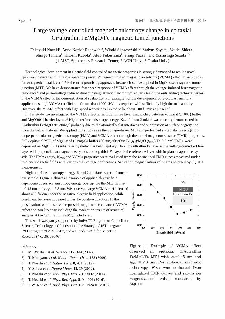
Technological development in electric-field control of magnetic properties is strongly demanded to realize novel spintronic devices with ultralow operating power. Voltage-controlled magnetic anisotropy (VCMA) effect in an ultrathin ferromagnetic metal layer1), 2) is the most promising approach, because it can be applied in MgO based magnetic tunnel junction (MTJ). We have demonstrated fast speed response of VCMA effect through the voltage-induced ferromagnetic resonance3) and pulse-voltage induced dynamic magnetization switching4) so far. One of the outstanding technical issues in the VCMA effect is the demonstration of scalability. For example, for the development of G-bit class memory applications, high VCMA coefficient of more than 1000 fJ/Vm is required with sufficiently high thermal stability. However, the VCMA effect with high speed response is limited to be about 100 fJ/Vm at present. 5) In this study, we investigated the VCMA effect in an ultrathin Fe layer sandwiched between epitaxial Cr(001) buffer and MgO(001) barrier layers.6) High interface anisotropy energy, Ki,0 of about 2 mJ/m2 was recently demonstrated in Cr/ultrathin Fe/MgO structure,7) probably due to the atomically flat interfaces and suppression of surface segregation from the buffer material. We applied this structure in the voltage-driven MTJ and performed systematic investigations on perpendicular magnetic anisotropy (PMA) and VCMA effect through the tunnel magnetoresistance (TMR) properties. Fully epitaxial MTJ of MgO seed (3 nm)/Cr buffer (30 nm)/ultrathin Fe (tFe)/MgO (tMgO)/Fe (10 nm)/Ta/Ru were deposited on MgO (001) substrates by molecular beam epitaxy. Here, the ultrathin Fe layer is the voltage-controlled free layer with perpendicular magnetic easy axis and top thick Fe layer is the reference layer with in-plane magnetic easy axis. The PMA energy, KPMA and VCMA properties were evaluated from the normalized TMR curves measured under in-plane magnetic fields with various bias voltage applications. Saturation magnetization value was obtained by SQUID measurement. High interface anisotropy energy, Ki,0 of 2.1 mJ/m2 was confirmed in our sample. Figure 1 shows an example of applied electric field dependene of surface anisotropy energy, KPMAtFe for the MTJ with tFe = 0.45 nm and tMgO = 2.8 nm. We observed large VCMA coefficient of about 400 fJ/Vm under the negative electric field application, while non-linear behavior appeared under the positive direction. In the presentation, we’ll discuss the possible origin of the enhanced VCMA effect and non-linearity including the evaluation results of structural analysis at the Cr/ultrathin Fe/MgO interfaces. This work was partly supported by ImPACT Program of Council for Science, Technology and Innovation, the Strategic AIST integrated R&D program “IMPULSE”, and a Grand-in-Aid for Scientific Research (No. 26709046). Reference 1) M. Weisheit et al. Science 315, 349 (2007). 2) T. Maruyama et al. Nature Nanotech. 4, 158 (2009). 3) T. Nozaki et al. Nature Phys. 8, 491 (2012). 4) Y. Shiota et al. Nature Mater. 11, 39 (2012). 5) T. Nozaki et al. Appl. Phys. Exp. 7, 073002 (2014). 6) T. Nozaki et al. Phys. Rev. Appl. 5, 044006 (2016). 7) J. W. Koo et al. Appl. Phys. Lett. 103, 192401 (2013).
Figure 1 Example of VCMA effect observed in epitaxial Cr/ultrathin Fe/MgO/Fe MTJ with tFe=0.45 nm and tMgO = 2.8 nm. Perpendicular magnetic anisotropy, KPMA was evaluated from normalized TMR curves and saturation magnetization value measured by SQUID.
-300 -200 -100 0 100 200 3000.32
0.36
0.40
0.44
0.48
0.52
KP
MAt F
e (m
J/m
2 )
Electric field (mV/nm)
Cr Ultrathin Fe
MgO Fe
5pA 7
7
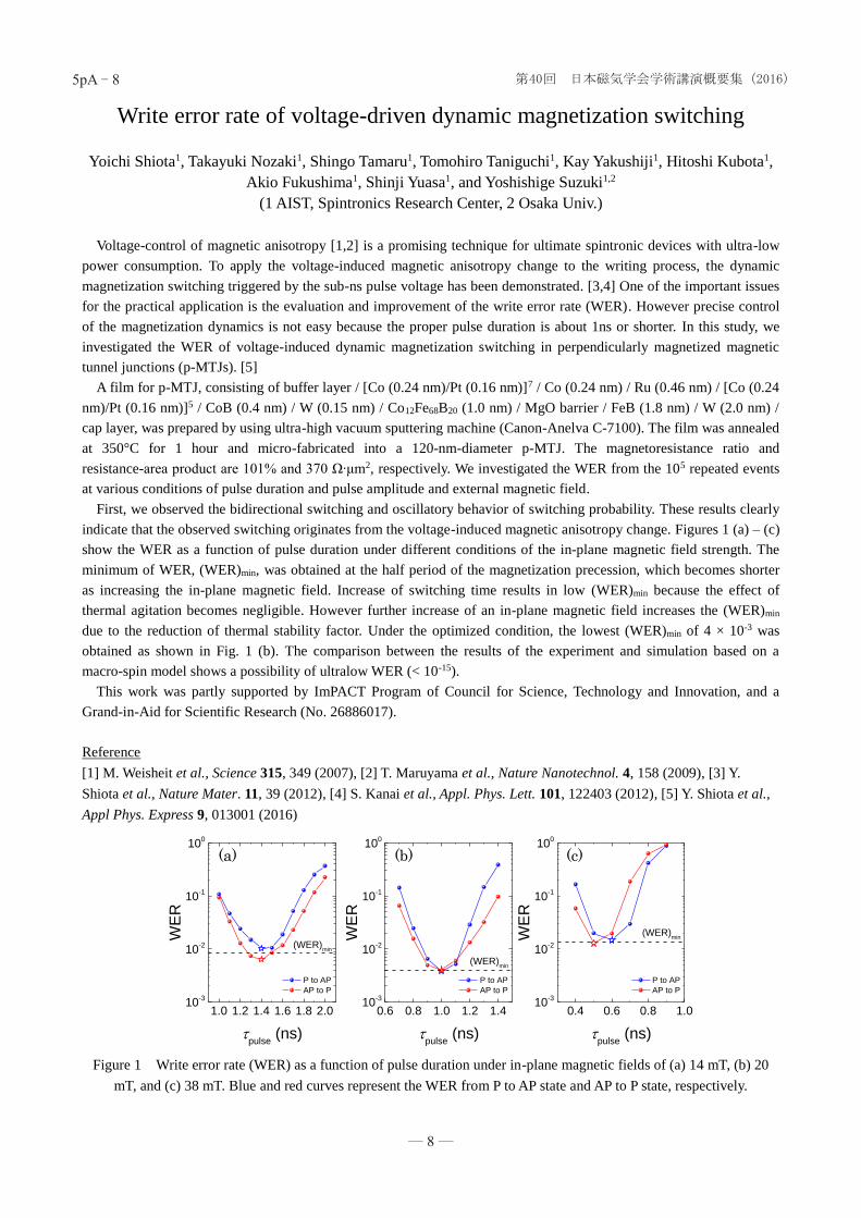
Write error rate of voltage-driven dynamic magnetization switching
1) R. Matsumoto, H. Arai, S. Yuasa, and H. Imamura: Appl. Phys.Express, 8, 063007 (2015).2) R. Matsumoto, H. Arai, S. Yuasa, and H. Imamura: Phys. Rev. B, 92, 140409(R) (2015).3) 本文中の数式における記号の意味は次の通りである : V と d は自由層の体積と厚さ, kB はボルツマン定数, T は絶対温度, α はギルバート・ダンピング定数, ℏはディラック定数, P はスピン分極率.
5pA 9
9
Deep etching microfabrication of perpendicularly magnetized MTJ
Akio Fukushima, Kay Yakushiji, Hitoshi Kubota, Shinji Yuasa
(AIST, Spintronics Research Center)
Low damage microfabrication is one of the most importance issue to fabricate higher density magnetic memory
devices. Etching process of the pillar part of magnetic tunnel junction (MTJ) is thought to be the main origin of the
processing damage. Argon ion beam etching has been used widely to fabricate the pillar part of MTJs because its
etching rate is not much sensitive to film materials. Reduction of the beam voltage of Ar ion beam etching is a straight
way to decrease the processing damage. Here, we report the deep etching microfabrication using low voltage Ar ion
beam etching, and some of the deep etched MTJs show enhancement of coercive field (Hc) and keep thermal activated
energy ().
We introduced new fabrication machine which is combining one etching chamber and two deposition chambers. This
machine makes possible to etch the pillar of MTJs and then to transfer the deposition chamber without breaking the
vacuum. The beam voltage and current of Ar ion beam is set to 150V and 45 mA, respectively. Low resistance
perpendicularly-magnetized MTJs [1] were used to estimate the process damage. We prepared a film of
perpendicularly-magnetized MTJ, which is consisting of buffer layer / [Co (0.24 nm)/Pt (0.16 nm)]9 / Co (0.24 nm) / Ru
(0.52 nm) / [Co (0.24 nm)/Pt (0.16 nm)]4 / W (0.1 nm) / CoB (0.4 nm) / W (0.1 nm) / FeB (1.1 nm) / MgO barrier / FeB
(~2 nm) / MgO cap / cap layer by ultra-high vacuum sputtering machine (Canon-Anelva C-7100). The top of the buffer
layer is about 50 nm-thick Ta layer. The film was annealed at 330°C for 1 hour, and then microfabricated into circular
MTJs with etching masks of 85, 75, 65 nm diameters. The resistance-area (RA) product of the film was 2.0 Ω∙μm2.
Two etching processes are tested; the first is standard etching where the MTJ film was etched down to just top of the
buffer layer; and the second is deep etching where the film was over etched into the middle of the buffer layer. The
etching depth was monitored by secondary ion mass spectrometer, but we need to care that the etching depth near the
pillar tends to be smaller than that of the plane part. The typical etching time for the standard etching is 30 min. and that
for the deep etching is about 50 min. After that, the pillar was covered by SiO2 layer without breaking the vacuum, and
then lift-offed the etching mask and made the top electrode.
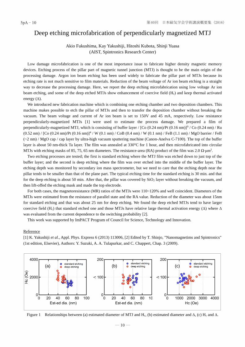
For both cases, the magnetoresistance (MR) ratios of the MTJs were 110~120% and well coincident. Diameters of the
MTJs were estimated from the resistance of parallel state and the RA value. Reduction of the diameter was about 15nm
for standard etching and that was about 25 nm for deep etching. We found the deep etched MTJs tend to have larger
coercive field (Hc) that standard etched one and those MTJs have relative large thermal activation energy () where
was evaluated from the current dependence to the switching probability [2].
This work was supported by ImPACT Program of Council for Science, Technology and Innovation.
Reference
[1] K. Yakushiji et al., Appl. Phys. Express 6 (2013) 113006, [2] Edited by T. Shinjo, "Nanomagnetims and Spintronics"
(1st edition, Elsevier), Authors: Y. Suzuki, A. A. Tulapurkar, and C. Chappert, Chap. 3 (2009).
Figure 1 Relationships between (a) estimated diameter of MTJ and Hc, (b) estimated diameter and , (c) Hc and .