36
Chang Liu MASS UIUC Micromachined Piezoelectric Devices Chang Liu Micro Actuators, Sensors, Systems Group University of Illinois at Urbana- Champaign
| Date post: | 19-Dec-2015 |
| Category: |
Documents |
| Upload: | spencer-edwards |
| View: | 230 times |
| Download: | 2 times |
Chang Liu MASSUIUC
Micromachined Piezoelectric Devices
Chang LiuMicro Actuators, Sensors, Systems Group
University of Illinois at Urbana-Champaign

Chang Liu MASSUIUC
Definition
• Direct Piezo Effect– a mechanical stress on a material produces an electrical
polarization• Inverse Piezo Effect
– an applied electric field in a material produces dimensional changes and stresses within a material.
• In general, both piezoelectricity and inverse piezoelectricity are denoted piezoelectric effects.
Chang Liu MASSUIUC
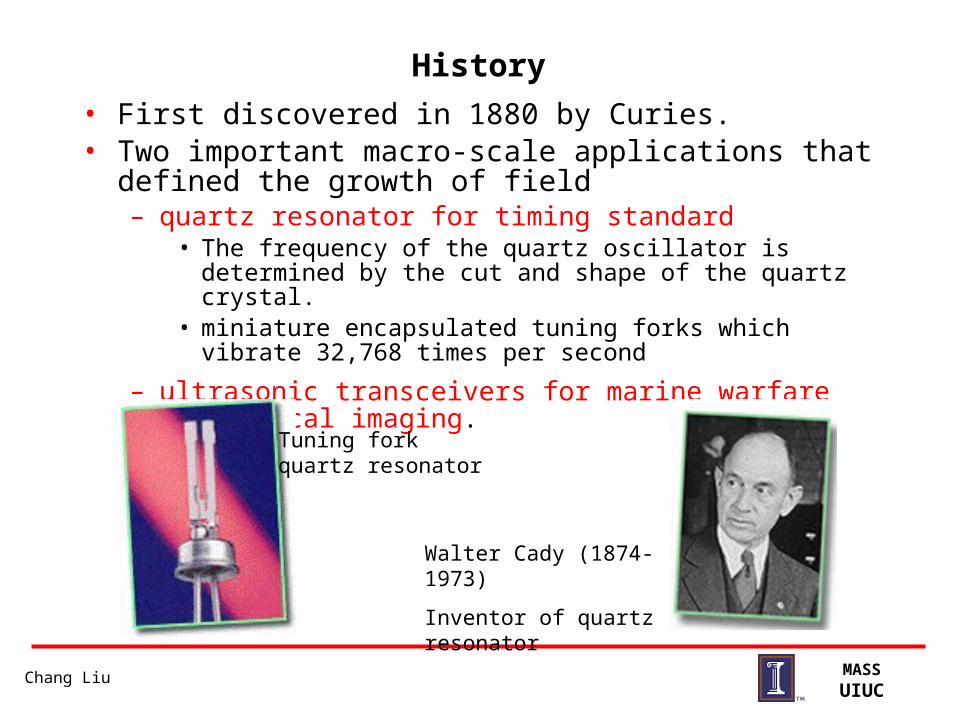
History
• First discovered in 1880 by Curies.• Two important macro-scale applications that defined the growth
of field– quartz resonator for timing standard
• The frequency of the quartz oscillator is determined by the cut and shape of the quartz crystal.
• miniature encapsulated tuning forks which vibrate 32,768 times per second
– ultrasonic transceivers for marine warfare and medical imaging.
Walter Cady (1874-1973)
Inventor of quartz resonator
Tuning forkquartz resonator
Chang Liu MASSUIUC
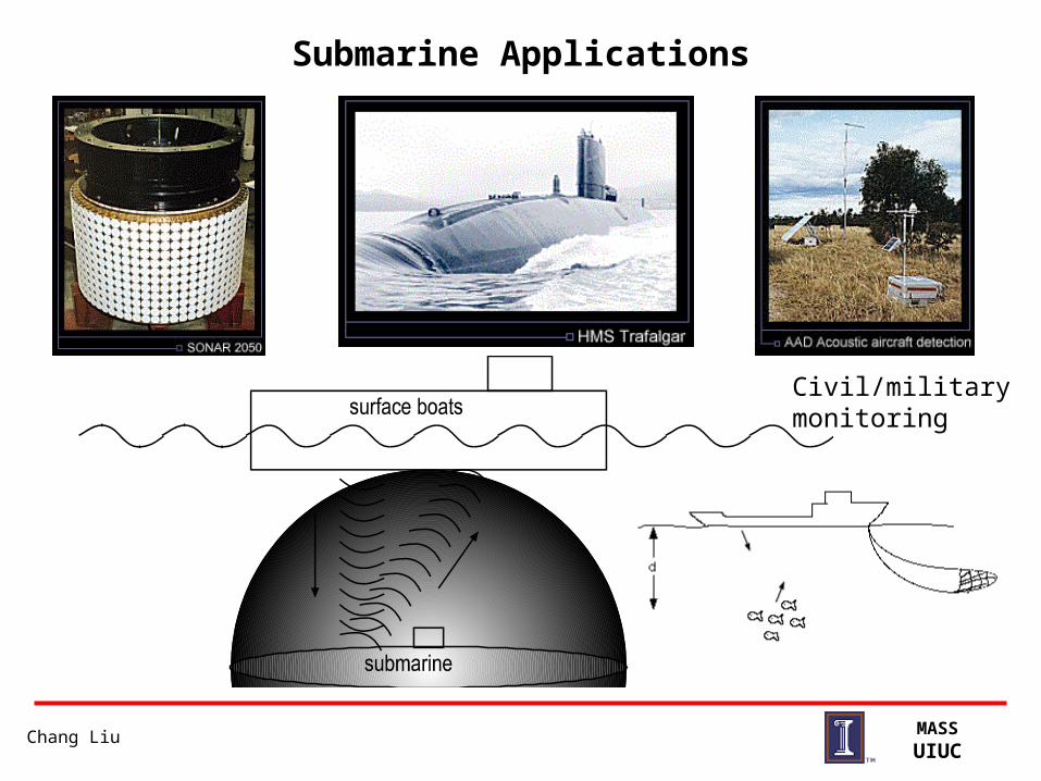
Submarine Applications
Civil/military monitoring
Chang Liu MASSUIUC
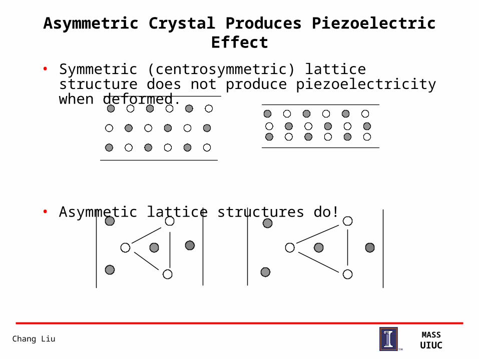
Asymmetric Crystal Produces Piezoelectric Effect
• Symmetric (centrosymmetric) lattice structure does not produce piezoelectricity when deformed.
• Asymmetic lattice structures do!
Chang Liu MASSUIUC
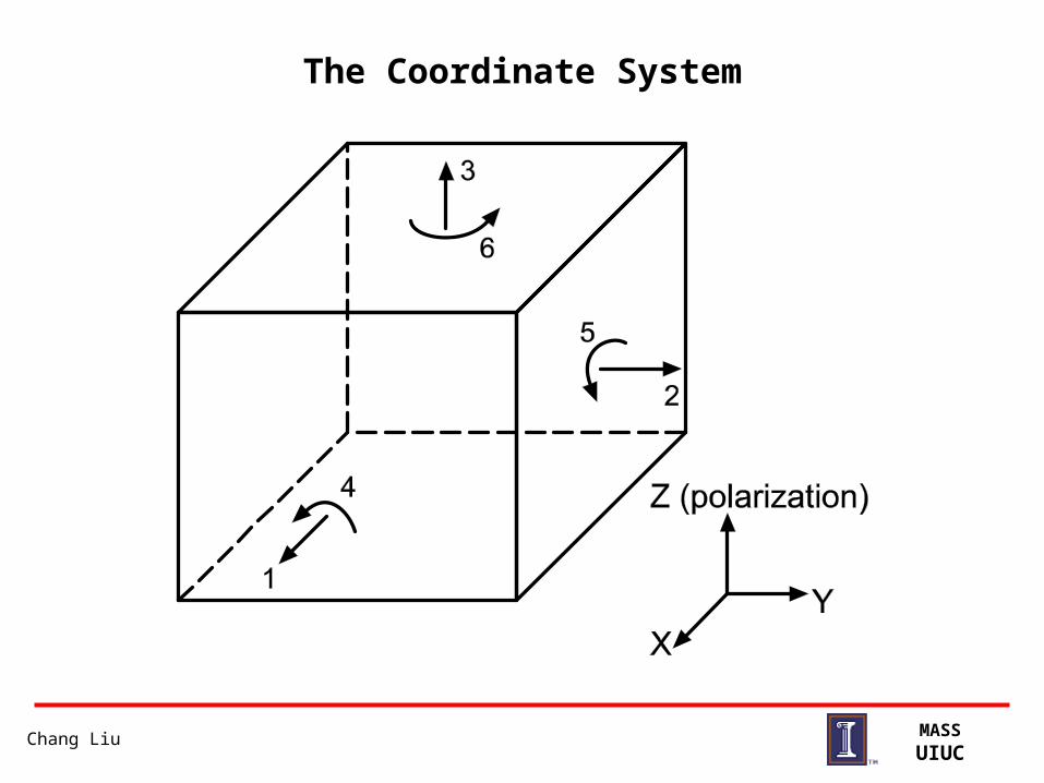
The Coordinate System

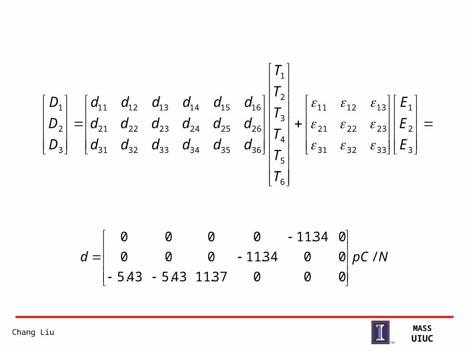
Chang Liu MASSUIUC
Direct
EdTD
3
2
1
333231
232221
131211
6
5
4
3
2
1
363534333231
262524232221
161514131211
3
2
1
E
E
E
T
T
T
T
T
T
dddddd
dddddd
dddddd
D
D
D
• D: Electrical Polarization• T: Applied Mechanical Stress• d: Piezoelectric Coefficient Matrix• ε: Electrical Permittivity Matrix• E: Electrical Field
Chang Liu MASSUIUC
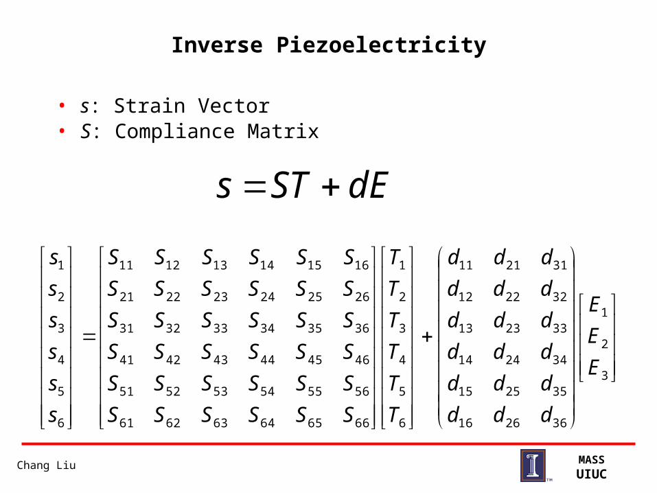
Inverse Piezoelectricity
• s: Strain Vector• S: Compliance Matrix
dESTs
3
2
1
362616
352515
342414
332313
322212
312111
6
5
4
3
2
1
666564636261
565554535251
464544434241
363534333231
262524232221
161514131211
6
5
4
3
2
1
E
E
E
ddd
ddd
ddd
ddd
ddd
ddd
T
T
T
T
T
T
SSSSSS
SSSSSS
SSSSSS
SSSSSS
SSSSSS
SSSSSS
s
s
s
s
s
s
Chang Liu MASSUIUC
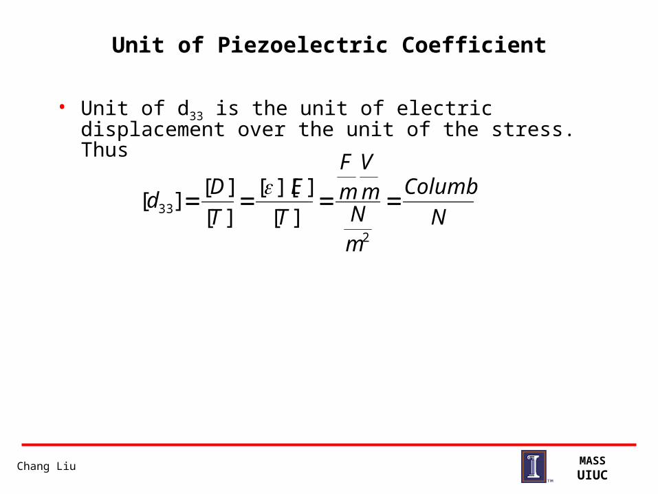
Unit of Piezoelectric Coefficient
• Unit of d33 is the unit of electric displacement over the unit of the stress. Thus
N
Columb
mN
mV
mF
T
E
T
Dd
2
33 ][
]][[
][
][][

Chang Liu MASSUIUC
Reverse Piezoelectricity
• Strain as a function of applied field is governed by
• Verify the unit
– charge multiplied by electric field is force.
3
2
1
000
0015
0150
3300
3100
3100
6
5
4
3
2
1
E
E
E
d
d
d
d
d
N
C
mV
C
C
mVE
d
)(
1
][
][][
Chang Liu MASSUIUC
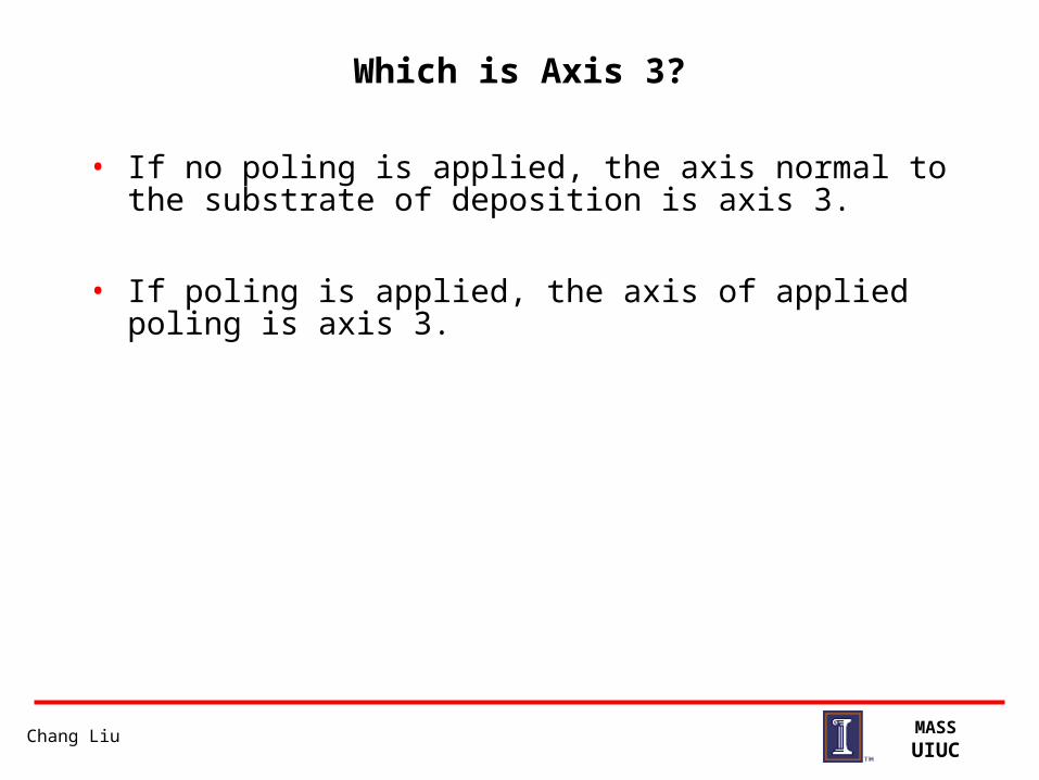
Which is Axis 3?
• If no poling is applied, the axis normal to the substrate of deposition is axis 3.
• If poling is applied, the axis of applied poling is axis 3.
Chang Liu MASSUIUC
Semiconductors – Are they piezoelectric?
• Si is symmetric and does not exhibit piezoelectricity.– (Si: positive charge; bond electrons: negative change)
• GaAs lattice is not symmetric and exhibits piezoelectricity.
Chang Liu MASSUIUC
Common Piezoelectric Materials
• ZnO– sputtered thin film– d33=246 pC/N
• Lead zirconate titanate (PZT)– ceramic bulk, or sputtering
thin film– d33=110 pC/N
• Quartz– bulk single crystal– d33=2.33 pC/N
• Polyvinylidene fluoride (PVDF)– polymer– d33=1.59 pC/N.
Diagram of a sputteringsystem.
Chang Liu MASSUIUC
Issues for Materials
• Poling– establishment of preferred sensing direction– application of electric field for long period of time after material is
formed• Curie temperature
– temperature above which the piezoelectric property will be lost.• Material purity
– the piezoelectric constant is sensitive to the composition of the material and can be damaged by defects.
• Frequency response– most materials have sufficient leakage and cannot “hold” a DC
force. The DC response is therefore not superior but can be improved by materials deposition/preparation conditions.
• Bulk vs thin film– bulk materials are easy to form but can not integrate with MEMS
or IC easily. Thin film materials are not as thick and overall displacement is limited.

Chang Liu MASSUIUC
Table 2: Properties of selected piezoelectric materials.
Material Relative permitivity(dielectric constant)
Young’s modulus
(GPa)
Density(kg/m3)
Coupling factor (k)
Curie temperature
(oC)
ZnO 8.5 210 5600 0.075 **
PZT-4(PbZrTiO3)
1300-1475 48-135 7500 0.6 365
PZT-5A(PbZrTiO3)
1730 48-135 7750 0.66 365
Quartz(SiO2)
4.52 107 2650 0.09 **
Lithium tantalate(LiTaO3)
41 233 7640 0.51 350
Lithium niobate(LiNbO3)
44 245 4640 ** **
PVDF 13 3 1880 0.2 80

Chang Liu MASSUIUC
Quartz
Nms /10
1.2990000
904.200000
0004.2005.45.4
0006.922.122.1
005.422.177.1279.1
005.422.179.177.12
212
NCd /10
000000
6.467.00000
0067.003.23.212
52.400
052.40
0052.4
r
Chang Liu MASSUIUC
PZT
• lead zirconate titanate (Pb(Zrx,Ti1-x)O3, or PZT) • Pb(Zr0.40,Ti0.60)TiO3
NpCd ij /
0001172.442.44
00293000
02930000

Chang Liu MASSUIUC
ZnO
NpCd /
00037.1143.543.5
0034.11000
034.110000
Chang Liu MASSUIUC
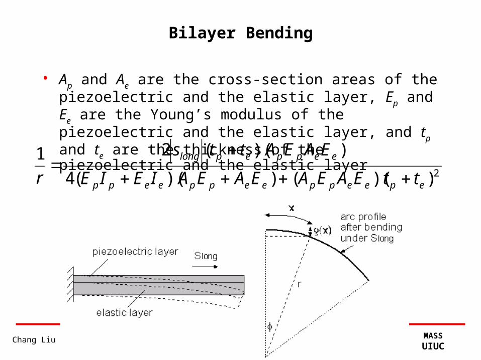
Bilayer Bending
• Ap and Ae are the cross-section areas of the piezoelectric and the elastic layer, Ep and Ee are the Young’s modulus of the piezoelectric and the elastic layer, and tp and te are the thickness of the piezoelectric and the elastic layer
2))(())((4
))((21
epeeppeeppeepp
eeppeplong
ttEAEAEAEAIEIE
EAEAtts
r
Chang Liu MASSUIUC
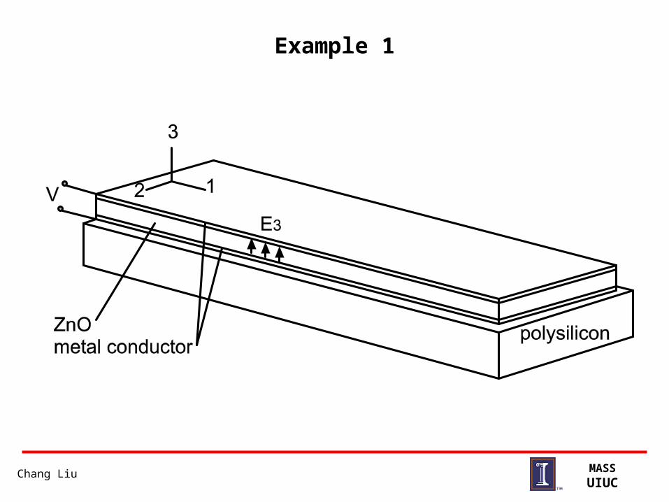
Example 1

Chang Liu MASSUIUC
Actuator Example
Cr/Au
Si3N4
ZnO
Si3N4
Cr
31

Chang Liu MASSUIUC
Example 2
• A patch of ZnO thin film is located near the base of a cantilever beam, as shown in the diagram below. The ZnO film is vertically sandwiched between two conducting films. The length of the entire beam is l. It consists of two segments – A and B. Segment A is overlapped with the piezoelectric material while segment B is not. The length of segments A and B are lA and lB, respectively. If the device is used as a force sensor, find the relationship between applied force F and the induced voltage.
Chang Liu MASSUIUC
3
2
1
333231
232221
131211
6
5
4
3
2
1
363534333231
262524232221
161514131211
3
2
1
E
E
E
T
T
T
T
T
T
dddddd
dddddd
dddddd
D
D
D
NpCd /
00037.1143.543.5
0034.11000
034.110000
Chang Liu MASSUIUC
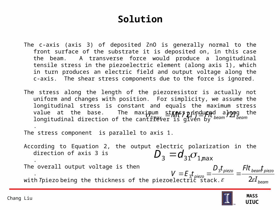
Solution
beambeam IFltIMt 2/)2/(max,1
max,1313 dD
beam
piezobeampiezopiezo I
tFlttDtEV
23
3
The c-axis (axis 3) of deposited ZnO is generally normal to the front surface of the substrate it is deposited on, in this case the beam. A transverse force would produce a longitudinal tensile stress in the piezoelectric element (along axis 1), which in turn produces an electric field and output voltage along the c-axis. The shear stress components due to the force is ignored.
The stress along the length of the piezoresistor is actually not uniform and changes with
position. For simplicity, we assume the longitudinal stress is constant and equals the maximum stress value at the base. The maximum stress induced along the longitudinal direction of the cantilever is given by
.The stress component is parallel to axis 1. According to Equation 2, the output electric polarization in the direction of axis 3 is
.The overall output voltage is then
.with Tpiezo being the thickness of the piezoelectric stack.
Chang Liu MASSUIUC
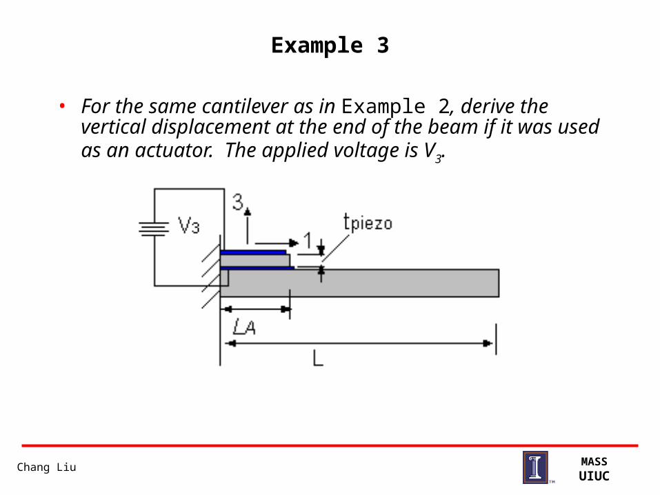
Example 3
• For the same cantilever as in Example 2, derive the vertical displacement at the end of the beam if it was used as an actuator. The applied voltage is V3.
Chang Liu MASSUIUC
piezot
VE 3
3
3131 dES
)( Alx
r
llx A
A )(
)(sin)()( ABA lxllxlx
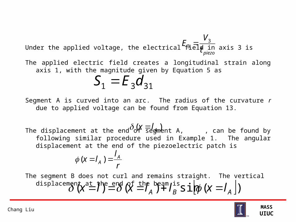
Under the applied voltage, the electrical field in axis 3 is
The applied electric field creates a longitudinal strain along axis 1, with the magnitude given by Equation 5 as
Segment A is curved into an arc. The radius of the curvature r due to applied voltage can be found from Equation 13.
The displacement at the end of segment A, , can be found by following similar procedure used in Example 1. The angular displacement at the end of the piezoelectric patch is
The segment B does not curl and remains straight. The vertical displacement at the end of the beam is
Chang Liu MASSUIUC
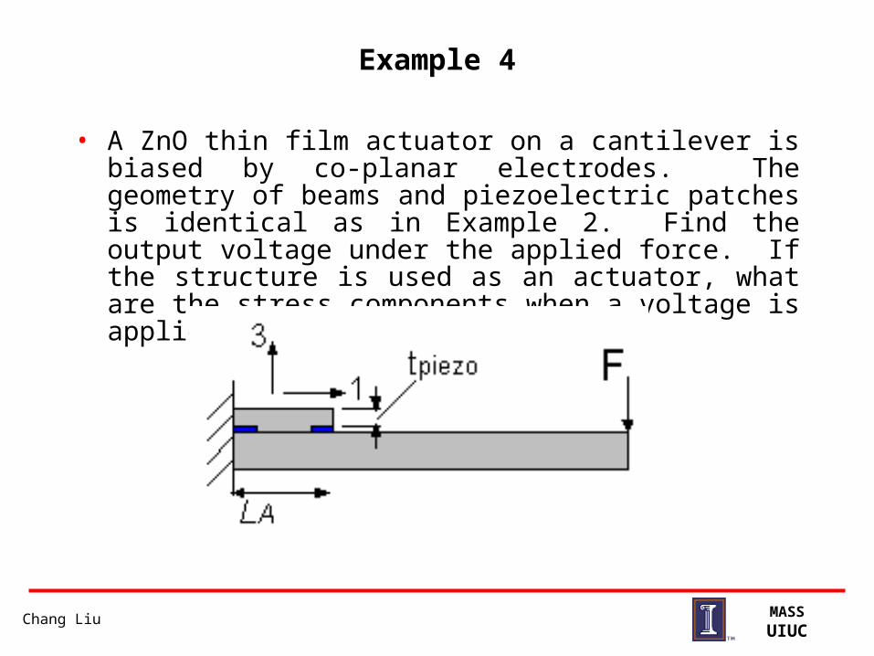
Example 4
• A ZnO thin film actuator on a cantilever is biased by co-planar electrodes. The geometry of beams and piezoelectric patches is identical as in Example 2. Find the output voltage under the applied force. If the structure is used as an actuator, what are the stress components when a voltage is applied across the electrodes?
Chang Liu MASSUIUC
3
2
1
333231
232221
131211
6
5
4
3
2
1
363534333231
262524232221
161514131211
3
2
1
E
E
E
T
T
T
T
T
T
dddddd
dddddd
dddddd
D
D
D
12
5
1
3
2
1
10
0
0
0
0
00037.1143.543.5
0034.11000
034.110000
T
T
D
D
D
512
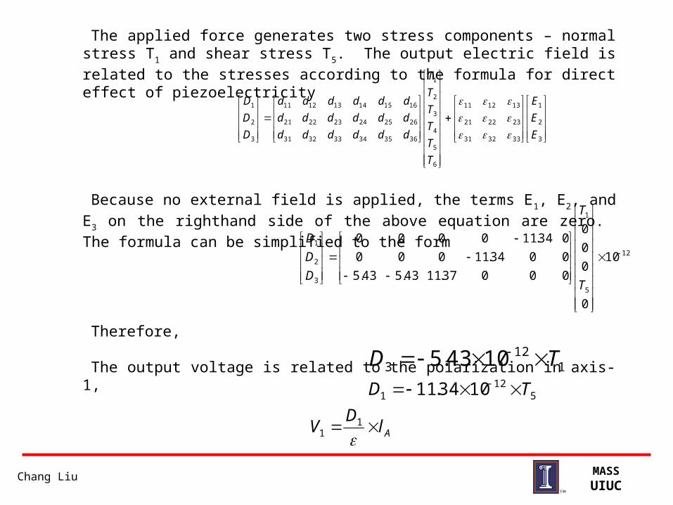
1 1034.11 TD 1
123 1043.5 TD
AlD
V
11
The applied force generates two stress components – normal stress T1 and shear stress
T5. The output electric field is related to the stresses according to the formula for direct
effect of piezoelectricity
Because no external field is applied, the terms E1, E2, and E3 on the righthand side of
the above equation are zero. The formula can be simplified to the form
Therefore,
The output voltage is related to the polarization in axis-1,

Chang Liu MASSUIUC
Let’s find the output stress when the device is used as an actuator. Suppose a voltage V is applied across the longitudinal direction. Here we assume the spacing between the two electrode is lA, hence the magnitude of the electric field is
The applied electric field creates a longitudinal strain along axis 1. The strain is found by
Since no external stresses are applied, we set T1 through T6 zero. The simplified formula for
strain is
No longitudinal strain components are generated in this manner.
Al
VE 1
3
2
1
362616
352515
342414
332313
322212
312111
6
5
4
3
2
1
666564636261
565554535251
464544434241
363534333231
262524232221
161514131211
6
5
4
3
2
1
E
E
E
ddd
ddd
ddd
ddd
ddd
ddd
T
T
T
T
T
T
ssssss
ssssss
ssssss
ssssss
ssssss
ssssss
s
s
s
s
s
s
0
0
0
0
0
10
0
0
000
0034.11
034.110
37.1100
43.500
43.500
5
121
6
5
4
3
2
1
S
E
s
s
s
s
s
s

Chang Liu MASSUIUC
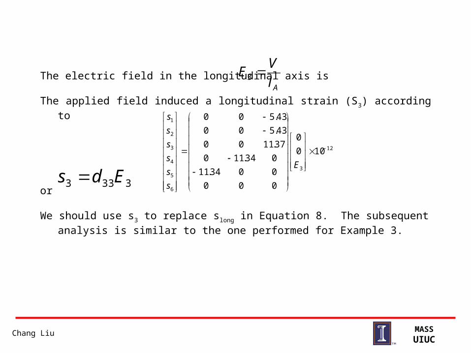
Example 5
• Derive the expression for the end displacement of piezoelectric transducer configured similarly as Example 4, with the difference that the electrodes are used to pole the ZnO material. In other words, axis-3 is now forced to lie in the longitudinal direction of the beam length. A voltage V is applied across two electrodes.
Chang Liu MASSUIUC
Al
VE 3
12
3
6
5
4
3
2
1
100
0
000
0034.11
034.110
37.1100
43.500
43.500
E
s
s
s
s
s
s
3333 Eds
The electric field in the longitudinal axis is
The applied field induced a longitudinal strain (S3) according to
or
We should use s3 to replace slong in Equation 8. The subsequent analysis is similar to the one
performed for Example 3.

Chang Liu MASSUIUC
Case 7.1: Acceleration Sensor

Chang Liu MASSUIUC
Case 7.2: Membrane Piezoelectric Accelerometer
Chang Liu MASSUIUC
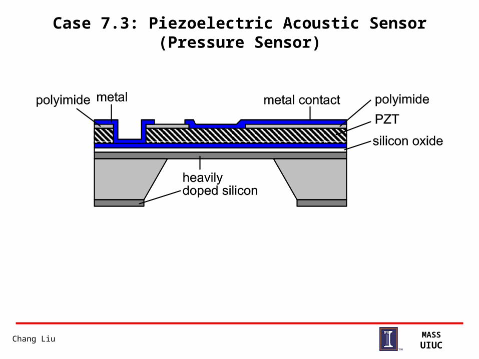
Case 7.3: Piezoelectric Acoustic Sensor (Pressure Sensor)
Chang Liu MASSUIUC
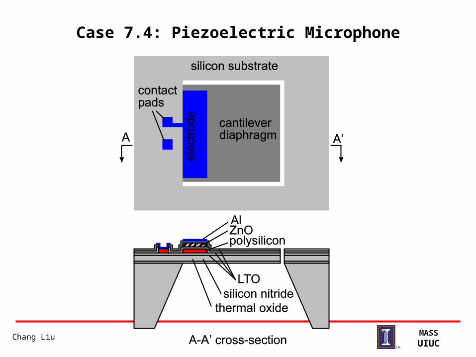
Case 7.4: Piezoelectric Microphone

Chang Liu MASSUIUC
Surface Elastic Waves


