226
Channel Isolated Thermocouple Input Module User's Manual -Q68TD-G-H01 -Q68TD-G-H02 -GX Configurator-TI (SW1D5C-QTIU-E)

Channel Isolated Thermocouple Input ModuleUser's Manual
-Q68TD-G-H01-Q68TD-G-H02-GX Configurator-TI (SW1D5C-QTIU-E)


SAFETY PRECAUTIONS(Read these precautions before using this product.)
Before using this product, please read this manual and the relevant manuals carefully and pay full attention
to safety to handle the product correctly.
In this manual, the safety precautions are classified into two levels: " WARNING" and " CAUTION".
Under some circumstances, failure to observe the precautions given under " CAUTION" may lead to
serious consequences.
Observe the precautions of both levels because they are important for personal and system safety.
Make sure that the end users read this manual and then keep the manual in a safe place for future
reference.
[Design Precautions]
WARNING● Do not write any data to the "system area" of the buffer memory in the intelligent function module.
Also, do not use any "use prohibited" signals as an output signal from the programmable controller
CPU to the intelligent function module.
Doing so may cause malfunction of the programmable controller system.
CAUTION● Do not install the control lines or communication cables together with the main circuit lines or power
cables.
Keep a distance of 100mm or more between them.
Failure to do so may result in malfunction due to noise.
WARNING
CAUTION
Indicates that incorrect handling may cause hazardous conditions,
resulting in death or severe injury.
Indicates that incorrect handling may cause hazardous conditions,
resulting in minor or moderate injury or property damage.
A - 1

[Installation Precautions]
[Wiring Precautions]
CAUTION● Use the programmable controller in an environment that meets the general specifications in the
user's manual for the CPU module used.
Failure to do so may result in electric shock, fire, malfunction, or damage to or deterioration of the
product.
● To mount the module, while pressing the module mounting lever located in the lower part of the
module, fully insert the module fixing projection(s) into the hole(s) in the base unit and press the
module until it snaps into place.
Incorrect mounting may cause malfunction, failure or drop of the module.
Fix the module to the base unit with a fixing bracket. (Q68TD-G-H02 only)
When using the programmable controller in an environment of frequent vibrations, fix the module
with a module fixing screw. (Q68TD-G-H01 only)
● Tighten the screw within the specified torque range.
Undertightening can cause drop of the screw, short circuit or malfunction.
Overtightening can damage the screw and/or module, resulting in drop, short circuit, or malfunction.
● Shut off the external power supply (all phases) used in the system before mounting or removing the
module.
Failure to do so may result in damage to the product.
A module can be replaced online (while power is on) on any MELSECNET/H remote I/O station or in
the system where a CPU module supporting the online module change function is used.
Note that there are restrictions on the modules that can be replaced online, and each module has its
predetermined replacement procedure.
For details, refer to the relevant chapter in this manual.
● Do not directly touch any conductive parts and electronic components of the module.
Doing so can cause malfunction or failure of the module.
CAUTION● Individually ground the shielded cables of the programmable controller with a ground resistance of
100 or less. Failure to do so may result in electric shock or malfunction.
● Connectors for external devices must be crimped or pressed with the tool specified by the
manufacturer, or must be correctly soldered.
Incomplete connections may cause short circuit, fire, or malfunction.
● Prevent foreign matter such as dust or wire chips from entering the module.
Such foreign matter can cause a fire, failure, or malfunction.
A - 2
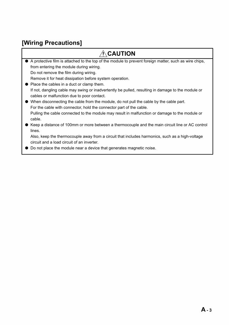
[Wiring Precautions]
CAUTION● A protective film is attached to the top of the module to prevent foreign matter, such as wire chips,
from entering the module during wiring.
Do not remove the film during wiring.
Remove it for heat dissipation before system operation.
● Place the cables in a duct or clamp them.
If not, dangling cable may swing or inadvertently be pulled, resulting in damage to the module or
cables or malfunction due to poor contact.
● When disconnecting the cable from the module, do not pull the cable by the cable part.
For the cable with connector, hold the connector part of the cable.
Pulling the cable connected to the module may result in malfunction or damage to the module or
cable.
● Keep a distance of 100mm or more between a thermocouple and the main circuit line or AC control
lines.
Also, keep the thermocouple away from a circuit that includes harmonics, such as a high-voltage
circuit and a load circuit of an inverter.
● Do not place the module near a device that generates magnetic noise.
A - 3

[Startup and Maintenance Precautions]
[Disposal Precautions]
WARNING● Do not touch any terminal while power is on.
Doing so will cause electric shock or malfunction.
● Shut off the external power supply (all phases) used in the system before cleaning the module or
retightening the terminal screws, connector screws, or module fixing screws.
Failure to do so may result in electric shock or cause the module to fail or malfunction.
Undertightening can cause drop of the screw, short circuit or malfunction.
Overtightening can damage the screw and/or module, resulting in drop, short circuit, or malfunction.
CAUTION● Do not disassemble or modify the modules.
Doing so may cause failure, malfunction, injury, or a fire.
● Shut off the external power supply (all phases) used in the system before mounting or removing the
module.
Failure to do so may cause the module to fail or malfunction.
A module can be replaced online (while power is on) on any MELSECNET/H remote I/O station or in
the system where a CPU module supporting the online module change function is used.
Note that there are restrictions on the modules that can be replaced online, and each module has its
predetermined replacement procedure.
For details, refer to the relevant chapter in this manual.
● After the first use of the product, do not mount/remove the module to/from the base unit more than
50 times (IEC 61131-2 compliant).
Exceeding the limit of 50 times may cause malfunction.
● Before handling the module, touch a grounded metal object to discharge the static electricity from
the human body.
Failure to do so may cause the module to fail or malfunction.
CAUTION● When disposing of this product, treat it as industrial waste.
A - 4

CONDITIONS OF USE FOR THE PRODUCT
(1) Mitsubishi programmable controller ("the PRODUCT") shall be used in conditions;
i) where any problem, fault or failure occurring in the PRODUCT, if any, shall not lead to any major
or serious accident; and
ii) where the backup and fail-safe function are systematically or automatically provided outside of
the PRODUCT for the case of any problem, fault or failure occurring in the PRODUCT.
(2) The PRODUCT has been designed and manufactured for the purpose of being used in general
industries.
MITSUBISHI SHALL HAVE NO RESPONSIBILITY OR LIABILITY (INCLUDING, BUT NOT
LIMITED TO ANY AND ALL RESPONSIBILITY OR LIABILITY BASED ON CONTRACT,
WARRANTY, TORT, PRODUCT LIABILITY) FOR ANY INJURY OR DEATH TO PERSONS OR
LOSS OR DAMAGE TO PROPERTY CAUSED BY the PRODUCT THAT ARE OPERATED OR
USED IN APPLICATION NOT INTENDED OR EXCLUDED BY INSTRUCTIONS, PRECAUTIONS,
OR WARNING CONTAINED IN MITSUBISHI'S USER, INSTRUCTION AND/OR SAFETY
MANUALS, TECHNICAL BULLETINS AND GUIDELINES FOR the PRODUCT.
("Prohibited Application")
Prohibited Applications include, but not limited to, the use of the PRODUCT in;
• Nuclear Power Plants and any other power plants operated by Power companies, and/or any
other cases in which the public could be affected if any problem or fault occurs in the PRODUCT.
• Railway companies or Public service purposes, and/or any other cases in which establishment of
a special quality assurance system is required by the Purchaser or End User.
• Aircraft or Aerospace, Medical applications, Train equipment, transport equipment such as
Elevator and Escalator, Incineration and Fuel devices, Vehicles, Manned transportation,
Equipment for Recreation and Amusement, and Safety devices, handling of Nuclear or
Hazardous Materials or Chemicals, Mining and Drilling, and/or other applications where there is a
significant risk of injury to the public or property.
Notwithstanding the above, restrictions Mitsubishi may in its sole discretion, authorize use of the
PRODUCT in one or more of the Prohibited Applications, provided that the usage of the PRODUCT
is limited only for the specific applications agreed to by Mitsubishi and provided further that no
special quality assurance or fail-safe, redundant or other safety features which exceed the general
specifications of the PRODUCTs are required. For details, please contact the Mitsubishi
representative in your region.
A - 5

REVISIONS
* The manual number is given on the bottom left of the back cover.
Japanese Manual Version SH-080794-F
© 2008 MITSUBISHI ELECTRIC CORPORATION
Print Date *Manual Number Revision
Nov., 2008 SH(NA)-080795ENG-A First printing
Sep., 2011 SH(NA)-080795ENG-B
SAFETY PRECAUTIONS, COMPLIANCE WITH EMC AND LOW VOLTAGE
DIRECTIVES, Section 6.2.3, WARRANTY
CONDITIONS OF USE FOR THE PRODUCT
Feb., 2012 SH(NA)-080795ENG-C
SAFETY PRECAUTIONS, GENERIC TERMS, ABBREVIATIONS, AND TERMS,
Chapter 1, Section 1.1, 2.1 to 2.3, 3.1, 3.2, 3.2.1, 3.2.4, 3.3.1, 3.3.2, 3.4.1, 3.4.4,
3.4.5, 3.4.10, 3.4.11, 4.1, 4.3, 4.4.1, 4.4.2, 4.5 to 4.7, 5.2.1, 5.2.2, 5.3.1, 5.4, 5.5,
5.6.1, 5.6.2, 6.2.1, 6.2.2, 6.3.2, 7.1, 7.2, 7.3.1 to 7.3.6, 7.4.1, 7.4.2, 7.5, 8.1,
8.2.9, Appendix 2.2 to 2.4, Appendix 3
Jun., 2016 SH(NA)-080795ENG-D
COMPLIANCE WITH EMC AND LOW VOLTAGE DIRECTIVES,
GENERIC TERMS, ABBREVIATIONS, AND TERMS, Section 2.1, 2.2, 2.3, 3.1,
3.2.1, 4.4.2, 5.2.2, 6.2, 6.2.2, 6.2.3, 6.3, 6.3.2, 6.3.3, 8.1, 8.2.1, 8.2.9
This manual confers no industrial property rights or any rights of any other kind, nor does it confer any patent licenses.
Mitsubishi Electric Corporation cannot be held responsible for any problems involving industrial property rights which may
occur as a result of using the contents noted in this manual.
Correction
Addition
Correction
Correction
A - 6

INTRODUCTION
Thank you for purchasing the MELSEC-Q series Programmable Controller.
Before using the equipment, please read this manual carefully to develop full familiarity with the functions
and performance of the Q series Programmable Controller you have purchased, so as to ensure correct
use.
Please forward a copy of this manual to the end user.
CONTENTS
SAFETY PRECAUTIONS .................................................................................................................................A - 1
CONDITIONS OF USE FOR THE PRODUCT..................................................................................................A - 5
REVISIONS.......................................................................................................................................................A - 6
INTRODUCTION...............................................................................................................................................A - 7
CONTENTS ......................................................................................................................................................A - 7
COMPLIANCE WITH EMC AND LOW VOLTAGE DIRECTIVES...................................................................A - 11
GENERIC TERMS, ABBREVIATIONS, AND TERMS....................................................................................A - 12
PACKING LIST ...............................................................................................................................................A - 14
CHAPTER 1 OVERVIEW 1 - 1 to 1 - 3
1.1 Features........................................................................................................................................... 1 - 2
CHAPTER 2 SYSTEM CONFIGURATION 2 - 1 to 2 - 7
2.1 Applicable Systems ......................................................................................................................... 2 - 1
2.2 When Using the Q68TD-G-H02 (H01) in the Redundant System ................................................... 2 - 4
2.3 How to Check the Function Version, Serial No., and Software Version .......................................... 2 - 5
CHAPTER 3 SPECIFICATIONS 3 - 1 to 3 - 62
3.1 Performance Specifications ............................................................................................................. 3 - 1
3.2 Function List .................................................................................................................................... 3 - 5
3.2.1 Temperature conversion system .............................................................................................. 3 - 7
3.2.2 Conversion setting for disconnection detection function (Q68TD-G-H02 only) ...................... 3 - 12
3.2.3 Disconnection state conversion setting function (Q68TD-G-H01 only) .................................. 3 - 14
3.2.4 Warning output function.......................................................................................................... 3 - 16
3.2.5 Cold junction temperature compensation resistor disconnection detection function .............. 3 - 21
3.3 I/O Signals Transferred to/from Programmable Controller CPU.................................................... 3 - 22
3.3.1 I/O signal list ........................................................................................................................... 3 - 22
3.3.2 I/O signal details ..................................................................................................................... 3 - 23
3.4 Buffer Memory ............................................................................................................................... 3 - 30
3.4.1 Buffer memory assignment..................................................................................................... 3 - 30
3.4.2 Conversion enable/disable setting (Un\G0)............................................................................ 3 - 38
3.4.3 CH[ ] Time/Count/Moving average/Time constant setting (Un\G1 to Un\G8)......................... 3 - 39
3.4.4 Conversion completion flag (Un\G10) .................................................................................... 3 - 40
3.4.5 CH[ ] Measured temperature value (Un\G11 to Un\G18) ....................................................... 3 - 41
A - 7

3.4.6 Error code (Un\G19) ............................................................................................................... 3 - 42
3.4.7 Setting range 1, 2 (Thermocouple type) (Un\G20,Un\G21) .................................................... 3 - 42
3.4.8 Setting range 3 (Offset/gain setting) (Un\G22) ....................................................................... 3 - 42
3.4.9 Averaging processing selection (Un\G24,Un\G25)................................................................. 3 - 43
3.4.10 Offset/gain setting mode (Un\G26,Un\G27)............................................................................ 3 - 44
3.4.11 CH[ ] Offset/gain temperature setting values (Un\G28 to Un\G43)......................................... 3 - 45
3.4.12 Cold junction compensation setting status (Un\G45) (Q68TD-G-H02 only) ........................... 3 - 45
3.4.13 Warning output enable/disable setting (Un\G46).................................................................... 3 - 46
3.4.14 Warning output flag (Process alarm/Rate alarm) (Un\G47,Un\G48) ...................................... 3 - 47
3.4.15 Disconnection detection flag (Un\G49) (Q68TD-G-H02 only)................................................. 3 - 48
3.4.16 Disconnection state monitor flag (Un\G49) (Q68TD-G-H01only) ........................................... 3 - 50
3.4.17 CH[ ] Scaling value (Un\G50 to Un\G57) ................................................................................ 3 - 52
3.4.18 Scaling valid/invalid setting (Un\G58) ..................................................................................... 3 - 53
3.4.19 CH[ ] Scaling range upper/lower limit values (Un\G62 to Un\G77)......................................... 3 - 54
3.4.20 CH[ ] Scaling width upper/lower limit values (Un\G78 to Un\G93).......................................... 3 - 55
3.4.21 CH[ ] Process alarm upper/lower limit values (Un\G94 to Un\G125)...................................... 3 - 56
3.4.22 CH[ ] Rate alarm warning detection period (Un\G126 to Un\G133)........................................ 3 - 57
3.4.23 CH[ ] Rate alarm upper/lower limit values (Un\G134 to Un\G149) ......................................... 3 - 57
3.4.24 Mode switching setting (Un\G158, Un\G159) ......................................................................... 3 - 58
3.4.25 Conversion setting for disconnection detection (Un\G164, Un\G165) (Q68TD-G-H02 only).. 3 - 59
3.4.26 Disconnection state conversion setting (Un\G164, Un\G165) (Q68TD-G-H01only)............... 3 - 60
3.4.27 CH[ ] Conversion setting value for disconnection detection (Un\G166 to Un\G173)
(Q68TD-G-H02 only) .............................................................................................................. 3 - 61
3.4.28 CH[ ] Conversion setting value for disconnection state (Un\G166 to Un\G173)
(Q68TD-G-H01only) ............................................................................................................... 3 - 61
3.4.29 Factory default offset/gain values, User range settings offset/gain values
(Un\G190 to Un\G253)............................................................................................................ 3 - 62
CHAPTER 4 SETUP AND PROCEDURES BEFORE OPERATION 4 - 1 to 4 - 20
4.1 Handling Precautions....................................................................................................................... 4 - 1
4.1.1 Fixing module with module fixing bracket (Q68TD-G-H02 only)............................................... 4 - 2
4.2 Setup and Procedures before Operation ......................................................................................... 4 - 3
4.3 Part Names...................................................................................................................................... 4 - 4
4.4 Wiring............................................................................................................................................... 4 - 7
4.4.1 Wiring precautions.................................................................................................................... 4 - 7
4.4.2 External wiring .......................................................................................................................... 4 - 8
4.5 Switch Setting for Intelligent Function Module............................................................................... 4 - 11
4.6 Offset/Gain Setting ........................................................................................................................ 4 - 13
4.7 Cold Junction Temperature Compensation with/without Setting ................................................... 4 - 19
CHAPTER 5 UTILITY PACKAGE (GX Configurator-TI) 5 - 1 to 5 - 23
5.1 Utility Package Functions ................................................................................................................ 5 - 1
5.2 Installing and Uninstalling the Utility Package ................................................................................. 5 - 3
5.2.1 Handling precautions................................................................................................................ 5 - 3
5.2.2 Operating environment ............................................................................................................. 5 - 5
5.3 Utility Package Operation ................................................................................................................ 5 - 7
5.3.1 Common utility package operations.......................................................................................... 5 - 7
A - 8

5.3.2 Operation overview................................................................................................................... 5 - 9
5.3.3 Starting the Intelligent function module utility ......................................................................... 5 - 11
5.4 Initial Setting .................................................................................................................................. 5 - 13
5.5 Auto Refresh Settings.................................................................................................................... 5 - 15
5.6 Monitoring/Test .............................................................................................................................. 5 - 17
5.6.1 Monitor/test screen ................................................................................................................. 5 - 17
5.6.2 Offset/gain setting operation................................................................................................... 5 - 20
5.6.3 OMC (Online Module Change) refresh data........................................................................... 5 - 23
CHAPTER 6 PROGRAMMING 6 - 1 to 6 - 30
6.1 Programming Procedure.................................................................................................................. 6 - 2
6.2 Using Programs in Normal System Configuration ........................................................................... 6 - 4
6.2.1 Before creating a program........................................................................................................ 6 - 6
6.2.2 Program example when Configurator-TI .................................................................................. 6 - 8
6.2.3 Program example when GX Configurator-TI is not used........................................................ 6 - 13
6.3 Using Programs on Remote I/O Network ...................................................................................... 6 - 17
6.3.1 Before creating a program...................................................................................................... 6 - 19
6.3.2 Program example when GX Configurator-TI is used.............................................................. 6 - 20
6.3.3 Program example when GX Configurator-TI is not used........................................................ 6 - 24
CHAPTER 7 ONLINE MODULE CHANGE 7 - 1 to 7 - 37
7.1 Online Module Change Conditions .................................................................................................. 7 - 2
7.2 Online Module Change Operations ................................................................................................. 7 - 3
7.3 Online Module Change Procedure .................................................................................................. 7 - 4
7.3.1 When factory default is used and initial setting was made with GX Configurator-TI ................ 7 - 4
7.3.2 When factory default is used and initial setting was made with sequence program................. 7 - 9
7.3.3 When user range setting is used and initial setting was made with GX Configurator-TI
(other system is available)...................................................................................................... 7 - 13
7.3.4 When user range setting is used and initial setting was made with GX Configurator-TI
(other system is unavailable).................................................................................................. 7 - 18
7.3.5 When user range setting is used and initial setting was made with sequence program
(other system is available)...................................................................................................... 7 - 23
7.3.6 When user range setting is used and initial setting was made with sequence program
(other system is unavailable).................................................................................................. 7 - 28
7.4 Range Reference Table................................................................................................................. 7 - 33
7.4.1 Range reference table (Q68TD-G-H02) ................................................................................. 7 - 33
7.4.2 Range reference table (Q68TD-G-H01) ................................................................................. 7 - 35
7.5 Precautions for Online Module Change......................................................................................... 7 - 37
CHAPTER 8 TROUBLESHOOTING 8 - 1 to 8 - 8
8.1 Error Code List................................................................................................................................. 8 - 1
8.2 Troubleshooting ............................................................................................................................... 8 - 4
8.2.1 "RUN" LED is extinguished ...................................................................................................... 8 - 4
8.2.2 "RUN" LED flickers ................................................................................................................... 8 - 4
8.2.3 "ERR" LED flickers ................................................................................................................... 8 - 4
A - 9

8.2.4 "ERR" LED is lit ........................................................................................................................ 8 - 4
8.2.5 "ALM" LED flickers.................................................................................................................... 8 - 5
8.2.6 "ALM" LED is lit......................................................................................................................... 8 - 5
8.2.7 When Disconnection detection signal (XC) (Q68TD-G-H02 only) or Disconnection state monitor
signal (XC) (Q68TD-G-H01 only) turns on................................................................................ 8 - 5
8.2.8 Measured temperature value cannot be read........................................................................... 8 - 5
8.2.9 Measured temperature value is abnormal ................................................................................ 8 - 6
8.2.10 Checking the Q68TD-G-H02(H01) status using GX Developer system monitor ...................... 8 - 7
APPENDICES APPX - 1 to APPX - 14
Appendix 1 Differences of Q68TD-G-H02, Q68TD-G-H01, Q64TD, Q64TDV-GH ..........................APPX - 1
Appendix 2 Dedicated Instruction.....................................................................................................APPX - 2
Appendix 2.1 Dedicated Instruction List and Available Device ...................................................APPX - 2
Appendix 2.2 G(P).OFFGAN.......................................................................................................APPX - 3
Appendix 2.3 G(P).OGLOAD ......................................................................................................APPX - 5
Appendix 2.4 G(P).OGSTOR ......................................................................................................APPX - 9
Appendix 3 External Dimension Diagram.......................................................................................APPX - 14
INDEX INDEX - 1 to INDEX - 2
A - 10

COMPLIANCE WITH EMC AND LOW VOLTAGE DIRECTIVES
(1) Method of ensuring complianceTo ensure that Mitsubishi programmable controllers maintain EMC and Low Voltage
Directives when incorporated into other machinery or equipment, certain measures
may be necessary. Please refer to one of the following manuals.
• QCPU User's Manual (Hardware Design, Maintenance and Inspection)
• Safety Guidelines
(This manual is included with the CPU module or base unit.)
The CE mark on the side of the programmable controller indicates compliance with
EMC and Low Voltage Directives.
(2) Additional measuresTo ensure that this product maintains EMC and Low Voltage Directives, please refer
to Section 4.4.1.
A - 11

GENERIC TERMS, ABBREVIATIONS, AND TERMS
Unless otherwise specified, this manual uses the following general terms, abbreviations,
and terms.
Generic term/
Abbreviation/TermDescription
Q68TD-G-H02 The abbreviation for the Q68TD-G-H02 channel isolated thermocouple input module
Q68TD-G-H01 The abbreviation for the Q68TD-G-H01 channel isolated thermocouple input module
Q68TD-G-H02(H01)The abbreviation for the Q68TD-G-H02 or Q68TD-G-H01 channel isolated thermocouple
input module
Up scaleThe maximum value in measured temperature range plus 5% value of measured
temperature range
Down scaleThe minimum value in measured temperature range minus 5% value of measured
temperature range
GX DeveloperThe product name of the software package for the MELSEC programmable controllers
GX Works2
GX Configurator-TIThe abbreviation for the thermocouple input module setting and monitor tool GX
Configurator-TI (SW1D5C-QTIU-E)
QCPU (Q mode)
A generic term for the Q00JCPU, Q00UJCPU, Q00CPU, Q00UCPU, Q01CPU,
Q01UCPU, Q02CPU, Q02HCPU, Q02PHCPU, Q02UCPU, Q03UDCPU, Q03UDVCPU,
Q03UDECPU, Q04UDHCPU, Q04UDVCPU, Q04UDEHCPU, Q06HCPU, Q06PHCPU,
Q06UDHCPU, Q06UDVCPU, Q06UDEHCPU, Q10UDHCPU, Q10UDEHCPU,
Q12HCPU, Q12PHCPU, Q12PRHCPU, Q13UDHCPU, Q13UDVCPU, Q13UDEHCPU,
Q20UDHCPU, Q20UDEHCPU, Q25HCPU, Q25PHCPU, Q25PRHCPU, Q26UDHCPU,
Q26UDVCPU, Q26UDEHCPU, Q50UDEHCPU, and Q100UDEHCPU
Redundant CPU A generic term for the Q12PRHCPU and Q25PRHCPU
Process CPU A generic term for the Q02PHCPU, Q06PHCPU, Q12PHCPU, and Q25PHCPU
Cold junction temperature
compensation resistor
A generic term for resistance temperature detectors (RTD) used for cold junction
temperature compensation. Pt100 is used.
Personal computer An IBM PC/AT® or compatible computer with DOS/V
Windows Vista®
A generic term for the following:
Microsoft® Windows Vista® Home Basic Operating System,
Microsoft® Windows Vista® Home Premium Operating System,
Microsoft® Windows Vista® Business Operating System,
Microsoft® Windows Vista® Ultimate Operating System,
Microsoft® Windows Vista® Enterprise Operating System
Windows® XP
A generic term for the following:
Microsoft® Windows® XP Professional Operating System,
Microsoft® Windows® XP Home Edition Operating System
A - 12

Windows® 7
A generic term for the following:
Microsoft® Windows® 7 Starter Operating System,
Microsoft® Windows® 7 Home Premium Operating System,
Microsoft® Windows® 7 Professional Operating System,
Microsoft® Windows® 7 Ultimate Operating System,
Microsoft® Windows® 7 Enterprise Operating System
Note that the 32-bit version is designated as "32-bit Windows® 7", and the 64-bit version
is designated as "64-bit Windows® 7".
Generic term/
Abbreviation/TermDescription
A - 13

A - 14
PACKING LIST
The product package contains the following.
(1) Q68TD-G-H02
(2) Q68TD-G-H01
Model Product Quantity
Q68TD-G-H02Q68TD-G-H02 channel isolated thermocouple input module 1
Cold junction temperature compensation resistor (RTD) 1
SW1D5C-QTIU-E GX Configurator-TI Version 1 (Single license product) (CD-ROM) 1
SW1D5C-QTIU-EA GX Configurator-TI Version 1 (Volume license product) (CD-ROM) 1
Model Product Quantity
Q68TD-G-H01Q68TD-G-H01 channel isolated thermocouple input module 1
Cold junction temperature compensation resistor (RTD) 1
SW1D5C-QTIU-E GX Configurator-TI Version 1 (Single license product) (CD-ROM) 1
SW1D5C-QTIU-EA GX Configurator-TI Version 1 (Volume license product) (CD-ROM) 1

1 OVERVIEW
1
OV
ER
VIE
W
2
SY
ST
EM
C
ON
FIG
UR
AT
ION
3
SP
EC
IFIC
AT
ION
S
4
SE
TU
P A
ND
P
RO
CE
DU
RE
S B
EF
OR
E
OP
ER
AT
ION
5
UT
ILIT
Y P
AC
KA
GE
(G
X
CO
NF
IGU
RA
TO
R-T
I)
6
PR
OG
RA
MM
ING
7
ON
LIN
E M
OD
ULE
C
HA
NG
E
8
TR
OU
BL
ES
HO
OT
ING
CHAPTER 1 OVERVIEW
This user's manual provides the specifications, handling instructions, programming
procedures and other information of the Q68TD-G-H02 or Q68TD-G-H01 channel isolated
thermocouple input module (hereafter abbreviated as Q68TD-G-H02 (H01)), which is
designed to use with the MELSEC-Q series CPU module (referred to as the
programmable controller CPU).
The Q68TD-G-H02(H01) is a module designed to convert thermocouple input values from
outside the programmable controller into 16-bit signed binary measured temperature
values and 16-bit signed binary scaling values (ratios).
Figure 1.1 Overview of Q68TD-G-H02(H01) * 1 Refer to Section 3.4.17 for details of the scaling values.
Q68TD-G-H02(H01)
Programmable
controller CPU
FROM
instruction
TO
instruction
Initial setting
Measured
temperature value,
scaling value
reading
(Buffer memory) Resistance temperaturedetector input(by cold junction temperaturecompensation resistor (RTD))
Thermocouple input
Thermocouple input
Set data
Measured
temperature value
Scaling value
Scaling value
Measured
temperature value
Cold junction
temperature
compensation
channel
Channel 1
Channel 8
Te
mp
era
ture
me
asu
rem
en
t
*1
*1
1 - 1

1 OVERVIEW
1.1 Features
(1) Channels isolatedQ68TD-G-H02(H01) is channel isolated modules.
(2) 8 channels of temperatures measured by one moduleOne Q68TD-G-H02(H01) module can measure temperatures of 8 channels.
It can also convert the detected temperature values into scaling values (ratios (%)).
(3) Setting of conversion enable/disableConversion enable/disable setting for each channel is possible. Disabling conversion
for unused channels prevents unnecessary disconnection detection or monitor of
disconnection state on unused channels.
(4) Use of thermocouples conforming to JIS or IEC standardsEight types of thermocouple (K, E, J, T, B, R, S, N) conforming to JIS or IEC standards
can be used.
A thermocouple type can be selected for each channel.
(5) Disconnection detection function (Q68TD-G-H02 only)Disconnection status of thermocouple or compensating lead wire can be detected for
each channel by Disconnection detection flag.
Disconnection status can also be detected from the measured temperature value by
setting "Up scale", "Down scale" or "Given value" for the Conversion setting for
disconnection detection.
(6) Disconnection monitor function (Q68TD-G-H01 only)Disconnection status of thermocouple or compensating lead wire can be checked on
each channel by Disconnection state monitor flag.
Disconnection status can also be checked from the measured temperature value by
setting "Up scale", "Down scale" or "Given value" for the Conversion setting for
disconnection detection.
(7) Selection of sampling processing, time average processing, count average processing, moving average processing, and primary delay filterAs a conversion processing method, sampling processing, time average processing,
count average processing, moving average or primary delay filter can be selected for
each channel.
(8) Cold junction temperature compensation by cold junction temperature compensation resistor (RTD)Cold junction temperature compensation is possible by connecting the supplied cold
junction temperature compensation resistor (RTD) and enabling the cold junction
temperature compensation.
Resistance temperature detector Pt100 is used for cold junction temperature
compensation resistor (RTD).
1 - 2 1.1 Features

1 OVERVIEW
1
OV
ER
VIE
W
2
SY
ST
EM
C
ON
FIG
UR
AT
ION
3
SP
EC
IFIC
AT
ION
S
4
SE
TU
P A
ND
P
RO
CE
DU
RE
S B
EF
OR
E
OP
ER
AT
ION
5
UT
ILIT
Y P
AC
KA
GE
(G
X
CO
NF
IGU
RA
TO
R-T
I)
6
PR
OG
RA
MM
ING
7
ON
LIN
E M
OD
ULE
C
HA
NG
E
8
TR
OU
BL
ES
HO
OT
ING
(9) Error compensation by offset/gain value settingError compensation can be made by setting offset and gain values on each channel.
As the offset and gain values, you can make selection from user range setting and
factory default setting.
(10)Warning output function
(a) Process alarm warning output
A warning can be output when the input range set by the user is exceeded.
Upper limit value and lower limit value can be set for each channel, and a setting
to have a difference (hysteresis) between warning output and warning clear is
also possible.
(b) Rate alarm warning output
By setting a changing rate, a warning can be output when the changing rate is
exceeded.
(11)Online module changeThe module can be changed without stopping the system.
Furthermore, the following operations can be processed by using sequence
programs.
• Transferring the offset/gain set values to the replacement Q68TD-G-H02 (H01)
• Transferring the offset/and gain set values to another Q68TD-G-H02 (H01)
mounted on the other slot
(12)Easy settings using GX Configurator-TIUsing GX Configurator-TI which is sold separately, sequence programs can be
reduced since settings of the Q68TD-G-H02 (H01) can be made on the screen.
Also, the set status or operating status of the module can be checked easily.
1.1 Features
1 - 3

2 SYSTEM CONFIGURATION
CHAPTER 2 SYSTEM CONFIGURATION
This chapter explains the system configuration of the Q68TD-G-H02 (H01).
2.1 Applicable Systems
This section describes applicable systems.
(1) Applicable modules and base units, and number of modules
(a) When mounted with a CPU module
For the CPU modules, the number of modules, and base units applicable to the
Q68TD-G-H02 (H01), refer to the user's manual for the CPU module used.
Note the following when the Q68TD-G-H02 (H01) is mounted with a CPU module.
• Depending on the combination with other modules or the number of mounted
modules, power supply capacity may be insufficient. Pay attention to the
power supply capacity before mounting modules, and if the power supply
capacity is insufficient, change the combination of the modules.
• Mount a module within the number of I/O points for the CPU module.
If the number of slots is within the available range, the module can be
mounted on any slot.
Remark
To use the Q68TD-G-H02 (H01) with a C Controller module, refer to the user's
manual for the C Controller module.
(b) When the module is used in a MELSECNET/H remote I/O station
For the MELSECNET/H remote I/O station, the number of modules, and base
units applicable to the Q68TD-G-H02 (H01), refer to the Q Corresponding
MELSECNET/H Network System Reference Manual (Remote I/O network).
(2) Restrictions on mountable slot position
(a) Restrictions in using both the Q68TD-G-H02 and Q68TD-G-H01
When mounting the Q68TD-G-H02 and Q68TD-G-H01 on the same base unit,
provide one or more than one slot of space between the Q68TD-G-H02 and
Q68TD-G-H01.
2 - 1 2.1 Applicable Systems

2 SYSTEM CONFIGURATION
1
OV
ER
VIE
W
2
SY
ST
EM
C
ON
FIG
UR
AT
ION
3
SP
EC
IFIC
AT
ION
S
4
SE
TU
P A
ND
P
RO
CE
DU
RE
S B
EF
OR
E
OP
ER
AT
ION
5
UT
ILIT
Y P
AC
KA
GE
(G
X
CO
NF
IGU
RA
TO
R-T
I)
6
PR
OG
RA
MM
ING
7
ON
LIN
E M
OD
ULE
C
HA
NG
E
8
TR
OU
BL
ES
HO
OT
ING
(b) Restriction on mountable slot position of the Q68TD-G-H01
The Q68TD-G-H01 has restrictions on mountable slot position.
The following describes the restrictions of the slot position when mounting the
Q68TD-G-H01 with a combination of the power supply module and the base unit.
For the slot that the Q68TD-G-H01 cannot be mounted, leave the slot open or
mount a module other than the Q68TD-G-H01.
The combination use of modules other than the following power supply modules
and the base units does not have restrictions.
When using the Q68TD-G-H01 on the remote I/O station, the restriction is the
same as for the main base unit.
When failing to comply with the following restrictions, the accuracy might not be in
the specification range.
1)
Figure 2.1 Mountable slot position of Q68TD-G-H01
2)
Figure 2.2 Mountable slot position of Q68TD-G-H01
3)
Figure 2.3 Mountable slot position of Q68TD-G-H01
Table 2.1 Restriction on mountable slot position
Power supply moduleRestrictions
Main base unit Extension base unit
Q63PNo restrictions
Mount the module to I/O slot No.1 or
later. 2)Q63RP
Q64P Mount the module to I/O slot No.1 or
later. 1)
Mount the module to I/O slot No.2 or
later. 3)Q64RP
OUT
I/01 I/01
CPUSlotNo.0
Not mountable Mountable
Power
supplySlotNo.1
SlotNo.2
OUT
I/01 I/01
IN
SlotNo.0
Not mountable Mountable
Power
supplySlotNo.1
SlotNo.2
OUTIN
I/01 I/01
SlotNo.0
Not mountable Mountable
SlotNo.1
SlotNo.2
Power
supply
2.1 Applicable Systems
2 - 2

2 SYSTEM CONFIGURATION
(3) Support of the multiple CPU systemWhen using the Q68TD-G-H02 (H01) in a multiple CPU system, refer to the following
manual first.
• QCPU User's Manual (Multiple CPU System).
(4) Compatibility with online module changeThe Q68TD-G-H02 (H01) is compatible with online module change from the initial
product with function version C.
Refer to CHAPTER 7.
(5) Supported software packagesRelation between the system containing the Q68TD-G-H02 (H01) and software
package is shown in the following table.
GX Developer or GX Works2 is required to use the Q68TD-G-H02 (H01).
POINTWhen using GX Works2, refer to the following:
• GX Works2 Version 1 Operating Manual (Common)
• GX Works2 Version 1 Operating Manual (Intelligent Function Module)
Table 2.2 System and compatible software package
SystemSoftware version
GX Developer GX Configurator-TI GX Works2
Q00J/Q00/Q01CPUSingle CPU system Version 7 or later
Version 1.28AE or later
(Q68TD-G-H02)
Version 1.24AA or later
(Q68TD-G-H01)Refer to the GX Works2
Version 1 Operating
Manual (Common).
Multiple CPU system Version 8 or later
Q02/Q02H/Q06H/Q12H/
Q25HCPU
Single CPU system Version 4 or later
Multiple CPU system Version 6 or later
Q02PH/Q06PHCPUSingle CPU system
Version 8.68W or laterMultiple CPU system
Q12PH/Q25PHCPUSingle CPU system
Version 7.10L or laterMultiple CPU system
Q12PRH/Q25PRHCPU Redundant system Version 8.45X or later
Q00UJ/Q00U/Q01UCPUSingle CPU system
Version 8.76E or laterMultiple CPU system
Q02U/Q03UD/Q04UDH/
Q06UDHCPU
Single CPU systemVersion 8.48A or later
Multiple CPU system
Q10UDH/Q20UDHCPUSingle CPU system
Version 8.76E or laterMultiple CPU system
Q13UDH/Q26UDHCPUSingle CPU system
Version 8.62Q or laterMultiple CPU system
Q03UDE/Q04UDEH/
Q06UDEH/Q13UDEH/
Q26UDEHCPU
Single CPU system
Version 8.68W or laterMultiple CPU system
Q10UDEH/Q20UDEHCPUSingle CPU system
Version 8.76E or laterMultiple CPU system
CPU modules other than the
above
Single CPU systemCannot be used Cannot be used
Multiple CPU system
If installed in a MELSECNET/H remote I/O station Version 6 or later
Version 1.28AE or later
(Q68TD-G-H02)
Version 1.24AA or later
(Q68TD-G-H01)
2 - 3 2.1 Applicable Systems

2 SYSTEM CONFIGURATION
1
OV
ER
VIE
W
2
SY
ST
EM
C
ON
FIG
UR
AT
ION
3
SP
EC
IFIC
AT
ION
S
4
SE
TU
P A
ND
P
RO
CE
DU
RE
S B
EF
OR
E
OP
ER
AT
ION
5
UT
ILIT
Y P
AC
KA
GE
(G
X
CO
NF
IGU
RA
TO
R-T
I)
6
PR
OG
RA
MM
ING
7
ON
LIN
E M
OD
ULE
C
HA
NG
E
8
TR
OU
BL
ES
HO
OT
ING
2.2 When Using the Q68TD-G-H02 (H01) in the Redundant System
This section describes the use of the Q68TD-G-H02 (H01) in the redundant system.
(1) Dedicated instructionThe dedicated instruction cannnot be used.
(2) GX Configurator-TIConfigurator-TI cannot be used when accessing Redundant CPU via an intelligent
function module on an extension base unit from GX Developer. Connect a personal
computer with a communication path indicated below.
Figure 2.4 Communication path available for GX Configurator-TI
Main base unit
Extension base unit
1 2
1 Direct connection to use the CPU
2 Connection through an intelligent function module on the main base unit
(Through Ethernet module, MELSECNET/H module, or CC-Link module)
(GX Configurator-TI cannot be used.)
2.2 When Using the Q68TD-G-H02 (H01) in the Redundant System
2 - 4

2 SYSTEM CONFIGURATION
2.3 How to Check the Function Version, Serial No., and Software Version
(1) Checking the function version and serial No.
(a) On the rating plate
The rating plate is put on the side of the Q68TD-G-H02 (H01).
Figure 2.5 Rating plate
(b) On the front of the module
The function version and serial No. on the rating plate is also indicated on the
front of the module (lower part).
11020
Function version
Serial No. (first 5 digits)
Relevant regulation
standards
Serial No.
Function version
2 - 5 2.3 How to Check the Function Version, Serial No., and Software Version

2 SYSTEM CONFIGURATION
1
OV
ER
VIE
W
2
SY
ST
EM
C
ON
FIG
UR
AT
ION
3
SP
EC
IFIC
AT
ION
S
4
SE
TU
P A
ND
P
RO
CE
DU
RE
S B
EF
OR
E
OP
ER
AT
ION
5
UT
ILIT
Y P
AC
KA
GE
(G
X
CO
NF
IGU
RA
TO
R-T
I)
6
PR
OG
RA
MM
ING
7
ON
LIN
E M
OD
ULE
C
HA
NG
E
8
TR
OU
BL
ES
HO
OT
ING
(c) On the system monitor (product information list)
To display the system monitor, select [Diagnostics] [System
monitor] of GX Developer.
Figure 2.6 "Product Information List" screen
1) Production number
Production number indication is not available for the Q68TD-G-H02 (H01); "-"
is shown.
Product Inf. List
Serial No.
Function version
Product No.
2.3 How to Check the Function Version, Serial No., and Software Version
2 - 6

2 SYSTEM CONFIGURATION
POINTThe serial No. on the rating plate and the front of the module may be different from
the serial No. displayed on the product information list in GX Developer.
• The serial No. on the rating plate and the front of the module indicates the
management information of the product.
• The serial No. displayed on the product information list in GX Developer
indicates the function information of the product. The function information
of the product is updated when a new function is added.
(2) Checking the software version of GX Configurator- TIThe software version of GX Configurator-TI can be checked on GX Developer by
clicking [Help] [Product information].
Figure 2.7 How to check the software version of GX Configurator- TI
("Product information" screen of GX Developer Version 8)
Software version
2 - 7 2.3 How to Check the Function Version, Serial No., and Software Version

3 SPECIFICATIONS
1
OV
ER
VIE
W
2
SY
ST
EM
C
ON
FIG
UR
AT
ION
3
SP
EC
IFIC
AT
ION
S
4
SE
TU
P A
ND
P
RO
CE
DU
RE
S B
EF
OR
E
OP
ER
AT
ION
5
UT
ILIT
Y P
AC
KA
GE
(G
X
CO
NF
IGU
RA
TO
R-T
I)
6
PR
OG
RA
MM
ING
7
ON
LIN
E M
OD
ULE
C
HA
NG
E
8
TR
OU
BL
ES
HO
OT
ING
CHAPTER 3 SPECIFICATIONS
3.1 Performance Specifications
The following are the performance specifications of the Q68TD-G-H02 (H01).
(1) List of performance specificationsTable 3.1 List of performance specifications
ItemSpecifications
Q68TD-G-H02 Q68TD-G-H01
Number of channels 8 channels
Output
Measured
temperature value16-bit signed binary (-2700 to 18200)
Scaling value 16-bit signed binary
Thermocouple compliance
standardsJIS C1602-1995,IEC 60584-1(1995),IEC60584-2(1982)
Applicable thermocouples,
conversion accuracy *1, and
effect from wiring resistance
of 1
Refer to (2) in this section
Cold junction compensation
accuracy *11.0
Accuracy *1 Caluculated with formula *2
Resolution B,R,S,N: 0.3 K,E,J,T: 0.1
Conversion speed *3 640ms/8 channels 320ms/8 channels
Sampling period *4 320ms/8 channels
Number of analog input
channels8 channels + cold junction compensation channels/ 1 module
Isolation specifications
Specific isolated areaIsolation
method
Dielectric withstand
voltageIsolation resistance
Between thermocouple input channel
and programmable controller power
supply
Transfer
isolation500VACrms for 1min
500VDC 10M or more
Between thermocouple input
channels
Trasnfer
isolation1000VACrms for 1min
Between cold junction compensation
channel and programmable controller
power supply
No isolation - -
Disconnection detection Available (each channel respectively)*5 Not available*6
Maximum number of writes to
flash memory50,000
Number of I/O points
occupied16 points (I/O assignment: Intelligent 16 points)
External interface 40-pin connector
Applicable wire size 0.3mm2(AWG22) or less (for A6CON1, A6CON4), 0.24mm2(AWG24) (for A6CON2)
External device connector
(sold separately)A6CON1, A6CON2, A6CON4
Internal current consumption
(5VDC)0.65A 0.49A
Weight 0.22kg 0.18kg
External dimensions 102(H) 27.4(W) 130(D)mm 98(H) 27.4(W) 90(D)mm
3.1 Performance Specifications
3 - 1

3 SPECIFICATIONS
* 1 To satisfy with the accuracy, a warm-up (power distribution) period of 30 minutes is required. * 2 Calculate the accuracy in the following method.
(Accuracy) = (conversion accuracy) + (temperature characteristic) (operating ambient temperature variation) + (cold junction temperature compensation accuracy)An operating ambient temperature variation indicates a deviation of the operating ambient
temperature from the 25 5 range.Example: When using the thermocouple B (refer to Section 3.1 (2)) with the operating ambient
temperature of 35 and the measured temperature of 1000 , the accuracy is as follows.
( 2.5 )+( 0.4 ) (35 -30 )+( 1 )= 5.5 * 3 The conversion speed indicates the maximum time from when the input temperature changes till
when the measured temperature value of buffer memory is batch-updated. * 4 The sampling period indicates the period batch-updating the measured temperature value in one
channel. * 5 When disconnection state is detected, output values are selected from "Up scale", "Down scale"
or Given scale". (Refer to Section 3.2.2) * 6 The Q68TD-G-H01 does not have the disconnection detection function. However, the
disconnection monitor function is available to select a measured temperature value on a disconnection occurrence from either "Up scale", "Down scale", or "Given value". (Refer to Section 3.2.3)It takes up to 11s to check a disconnection state.
3 - 2 3.1 Performance Specifications

3 SPECIFICATIONS
1
OV
ER
VIE
W
2
SY
ST
EM
C
ON
FIG
UR
AT
ION
3
SP
EC
IFIC
AT
ION
S
4
SE
TU
P A
ND
P
RO
CE
DU
RE
S B
EF
OR
E
OP
ER
AT
ION
5
UT
ILIT
Y P
AC
KA
GE
(G
X
CO
NF
IGU
RA
TO
R-T
I)
6
PR
OG
RA
MM
ING
7
ON
LIN
E M
OD
ULE
C
HA
NG
E
8
TR
OU
BL
ES
HO
OT
ING
(2) Applicable thermocouples, conversion accuracy, and effect from wiring resistance of 1The following table lists applicable thermocouples, conversion accuracy, and the
effect from wiring resistance of 1.
Table 3.2 Applicable thermocouples, conversion accuracy, and the effect from wiring resistance of 1
Usable
Thermo
couple
Type
Measured
Temperature
Range*1
Conversion Accuracy
(At operating ambient
temperature 25 5 )
Temperature Characteristic
(Per operating ambient
temperature variation of
1 )
Max. Temperature
Error at Ambient
Temperature 55
Effect from wiring
resistance of 1*4
(upper: Q68TD-G-H02
lower: Q68TD-G-H01)
B
0 to 600 ------*3 ------*3 ------*3 ------*3
600 to 800 *2 3.0
0.4
13.0-0.169 /
-0.042 /
800 to 1700 *2 2.5 12.5-0.143 /
-0.036 /
1700 to 1820 ------*3 ------*3 ------*3 ------*3
R
-50 to 0 ------*3 ------*3 ------*3 ------*3
0 to 300 *2 2.5 0.4 12.5-0.200 /
-0.050 /
300 to 1600 *2 2.0 0.3 9.5-0.112 /
-0.028 /
1600 to 1760 ------*3 ------*3 ------*3 ------*3
S
-50 to 0 ------*3 ------*3 ------*3 ------*3
0 to 300 *2 2.5 0.4 12.5-0.200 /
-0.050 /
300 to 1600 *2 2.0 0.3 9.5-0.112 /
-0.028 /
1600 to 1760 ------*3 ------*3 ------*3 ------*3
K
-270 to -200 ------*3 ------*3 ------*3 ------*3
-200 to 0 *2
Larger value of 0.5 and
0.5% of measured
temperature
Larger value of 0.06 and
0.2% of measured
temperature
11.0
-0.034 /
-0.009 /
0 to 1200 *2
Larger value of 0.25
and
0.5% of measured
temperature
Larger value of 0.06 and
0.02% of measured
temperature
9.0
-0.026 /
-0.007 /
1200 to 1370 ------*3 ------*3 ------*3 ------*3
E
-270 to -200 ------*3 ------*3 ------*3 ------*3
-200 to 0 *2
Larger value of 0.5 and
0.5% of measured
temperature
Larger value of 0.06 and
0.15% of measured
temperature
8.5
-0.023 /
-0.006 /
0 to 900 *2
Larger value of 0.5 and
0.25% of measured
temperature
Larger value of 0.06 and
0.02% of measured
temperature
6.75
-0.018 /
-0.005 /
900 to 1000 ------*3 ------*3 ------*3 ------*3
J
-210 to -40 ------*3 ------*3 ------*3 ------*3
-40 to 750 *2
Larger value of 0.5 and
0.25% of measured
temperature
Larger value of 0.06 and
0.02% of measured
temperature
5.625
-0.022 /
-0.006 /
750 to 1200 ------*3 ------*3 ------*3 ------*3
3.1 Performance Specifications
3 - 3

3 SPECIFICATIONS
* 1 If a value entered from the thermocouple is outside the measured temperature range given in the table, it is handled as the maximum/minimum value of the measured temperature range.
* 2 The accuracies only in the temperature ranges of Class 1 to 3 (shaded areas) in JIS C1602-1995 apply.Also, a warm-up (power distribution) period of 30 minutes is required to satisfy with the accuracy.
* 3 Temperature measurement can be executed, but accuracy is not guaranteed. * 4 This is the temperature error per 1 wiring resistance of the thermocouple. Check the wiring
resistance value and calculate the temperature error in the system. If the error exceeds the allowable range of the system, correct the measured temperature value by the offset/gain setting. (Refer to Section 4.6.)
T
-270 to -200 ------*3 ------*3 ------*3 ------*3
-200 to 0 *2
Larger value of 0.5 and
0.5% of measured
temperature
Larger value of 0.06 and
0.1% of measured
temperature
6.0
-0.036 /
-0.009 /
0 to 350 *2
Larger value of 0.5 and
0.25% of measured
temperature
Larger value of 0.06 and
0.02% of measured
temperature
2.625
-0.026 /
-0.007 /
350 to 400 ------*3 ------*3 ------*3 ------*3
N
-270 to -200 ------*3 ------*3 ------*3 ------*3
-200 to 0 *2
Larger value of 0.5 and
0.5% of measured
temperature
Larger value of 0.06 and
0.2% of measured
temperature
11.0
-0.048 /
-0.012 /
0 to 1250 *2
Larger value of 0.5 and
0.25% of measured
temperature
Larger value of 0.06 and
0.02% of measured
temperature
9.375
-0.039 /
-0.010 /
1250 to 1300 ------*3 ------*3 ------*3 ------*3
Table 3.2 Applicable thermocouples, conversion accuracy, and the effect from wiring resistance of 1
3 - 4 3.1 Performance Specifications

3 SPECIFICATIONS
1
OV
ER
VIE
W
2
SY
ST
EM
C
ON
FIG
UR
AT
ION
3
SP
EC
IFIC
AT
ION
S
4
SE
TU
P A
ND
P
RO
CE
DU
RE
S B
EF
OR
E
OP
ER
AT
ION
5
UT
ILIT
Y P
AC
KA
GE
(G
X
CO
NF
IGU
RA
TO
R-T
I)
6
PR
OG
RA
MM
ING
7
ON
LIN
E M
OD
ULE
C
HA
NG
E
8
TR
OU
BL
ES
HO
OT
ING
3.2 Function List
The following table lists the Q68TD-G-H02 (H01) functions.
Table 3.3 Function list
Item Description Refer To
Temperature conversion
function
This function allows temperature data to be imported by connecting a thermocouple.
Temperature data are 16-bit signed binary (-2700 to 18200) and stored into buffer memory.Section 3.4.5
Temperature conversion
system
(1) Sampling processing
Section 3.2.1
A temperature input value is converted one by one on each channel and a measured
temperature value is output after every conversion. Then the value is stored into buffer
memory.
(2) Averaging processing
This processing averages a measured temperature value for each channel and the
averaged value is stored into buffer memory.
Averaging processing contains three methods as described below.
(a) Time average
(b) Count average
(c) Moving average
(3) Primary delay filter
Measured temperature values are smoothed by a preset time constant.
Conversion enable/disable
function
This function specifies whether temperature conversion is enabled or disabled on each
channel.Section 3.4.2
Thermocouple type
selection functionThis function sets the type of thermocouple on each channel. Section 4.5
Disconnection detection
function
(Q68TD-G-H02 only)
This function checks the disconnection of the connected thermocouple on each conversion-
enabled channel.Section 3.4.15
Conversion setting for
disconnection detection
function
(Q68TD-G-H02 only)
This function is to select a value to be stored in the CH Measured temperature value
(Un\G11 to Un\G18) from "Up scale", "Down scale" or "Given scale" when disconnection is
detected.
Section 3.2.2
Disconnection monitor
function
(Q68TD-G-H01 only)
This function checks the disconnection of the connected thermocouple on each conversion-
enabled channel.Section 3.4.16
Disconnection state
conversion setting function
(Q68TD-G-H01 only)
This function is to select a value to be stored in the CH Measured temperature value
(Un\G11 to Un\G18) from "Up scale", "Down scale" or "Given scale" when disconnection is
detected.
Section 3.2.3
Cold junction temperature
compensation with/without
setting function
This function determines whether to use cold junction temperature compensation.
Use this function to measure temperature in higher accuracy than the cold junction
temperature compensation accuracy ( 1 ) by the cold junction temperature
compensation resistor (RTD) that is included with the Q68TD-G-H02 (H01).
The cold junction temperature compensation accuracy can be improved by disabling the
cold junction temperature compensation and providing a precision ice bath externally.
Section 4.7
Cold junction temperature
compensation resistor
disconnection detection
function
This function detects a disconnection of connected cold junction temperature compensation
resistor (RTD).Section 3.2.5
Warning output function
(1)
(2)
Process alarm
A warning is output when the measured temperature value is equal to or more than the
process alarm upper upper limit value, or equal to or less than the process alarm lower
lower limit value.
Rate alarm
A warning is output when the measured temperature value changes in a rate by which
the measured temperature value reaches the rate alarm upper limit value or more, or
the rate alarm lower limit value or less.
Section 3.2.4
3.2 Function List
3 - 5

3 SPECIFICATIONS
Scaling functionThis function can convert a measured temperature value into a preset range ratio (%) and
import it into buffer memory.
Section 3.4.17
to
Section 3.4.20
Offset/gain setting function This function compensates an error of measured temperature value.Section 3.4.11
Section 4.6
Online module change A module change is made without the system being stopped. CHAPTER 7
Table 3.3 Function list
Item Description Refer To
3 - 6 3.2 Function List

3 SPECIFICATIONS
1
OV
ER
VIE
W
2
SY
ST
EM
C
ON
FIG
UR
AT
ION
3
SP
EC
IFIC
AT
ION
S
4
SE
TU
P A
ND
P
RO
CE
DU
RE
S B
EF
OR
E
OP
ER
AT
ION
5
UT
ILIT
Y P
AC
KA
GE
(G
X
CO
NF
IGU
RA
TO
R-T
I)
6
PR
OG
RA
MM
ING
7
ON
LIN
E M
OD
ULE
C
HA
NG
E
8
TR
OU
BL
ES
HO
OT
ING
3.2.1 Temperature conversion system
(1) Temperature conversion of Q68TD-G-H02(H01)
(a) Sampling period
The Q68TD-G-H02(H01) measures the temperature from CH1 to CH8 every
40ms per channel.
The sampling period indicates the period (320ms) batch-updating the measured
temperature value in one channel in the case of that the sampling processing is
specified with the Averaging processing selection (Un\G24 and Un\G25).
Regardless of the number of conversion-enabled channels, the measured
temperature values are stored in the buffer memory every 320ms.
(b) Conversion speed
The conversion speed indicates the maximum time required before the measured
temperature values are stored into the buffer memory.
The following figure shows the timing of storing the measured temperature values
of Q68TD-G-H02 and Q68TD-G-H01 respectively.
Figure 3.1 Q68TD-G-H01 and Q68TD-G-H02 conversion speed overview
(2) Sampling processingMeasured temperature value that is measured at every 320ms of sampling period is
stored in the buffer memory.
Input temperature input
from outside to CH1
Measured temperature
value of CH1 in the
Q68TD-G-H01
Measured temperature
value of CH1 in the
Q68TD-G-H02
Maximum 320ms
Maximum 640ms
1) 2)
3) 4)
CH1 CH1 CH1 CH1CH2 CH8
CH1 CH1 CH1 CH1CH2 CH8
Trend of CH1 input
temperature (A)
At this point, the CH1
measured temperature
value of the buffer memory,
which is measured with
the trend of (A), is stored.
At this point, the CH1
measured temperature
value of the buffer memory,
which is measured with
the trend of (A), is stored.
Sampling period
(320ms)
The measured temperature
value of 1) is stored
The measured temperature
value of 2) is stored
The measured temperature
value of 3) is stored
The measured temperature
value of 1) is stored
The measured temperature
value of 2) is stored
The measured temperature
value of 3) is stored
The measured temperature
value of 4) is stored
Sampling period
(320ms)
Sampling period
(320ms)
Sampling period
(320ms)
3.2 Function List3.2.1 Temperature conversion system
3 - 7

3 SPECIFICATIONS
(3) Averaging processingAfter the first averaging processing is completed, the corresponding bit for a channel
where processing has been completed of the Conversion completion flag (Un\G10)
turns ON (changes to "1").
(a) Time average
Conversion is executed for a period of set time, and the total value, which
excludes the maximum and the minimum values, is averaged and stored in the
buffer memory.
The number of processing times within the set time is below.
Number of processing times (times) = set time sampling period (320ms)
Setting range of time average is 1280 to 5000ms.
If a value outside the setting range is set, an error (error code: 20 ) occurs.
[Example]
When six channels, channels 1, 2, 3, 4, 5, 6, are enabled for conversion and the
set time is 2000ms, measurement is executed for six times and the average value
is output.
2000 320 =6.25 (times)...... Drop the fractional part
(b) Count average
Conversion is executed for a preset number of times, and the total value
excluding the maximum and the minimum values is averaged and stored in the
buffer memory.
The processing time is below.
Processing time = set count 320(ms)
Setting range of count average is 4 to 500 times.
If a value outside the setting range is set, an error (error code: 30 ) occurs.
[Example]
When six channels, channels 1, 2, 3, 4, 5, 6, are enabled for conversion and the
count averaging is set to 5 times, the average value is output for every 1600(ms).
5 320 = 1600 (ms)
3 - 8 3.2 Function List3.2.1 Temperature conversion system

3 SPECIFICATIONS
1
OV
ER
VIE
W
2
SY
ST
EM
C
ON
FIG
UR
AT
ION
3
SP
EC
IFIC
AT
ION
S
4
SE
TU
P A
ND
P
RO
CE
DU
RE
S B
EF
OR
E
OP
ER
AT
ION
5
UT
ILIT
Y P
AC
KA
GE
(G
X
CO
NF
IGU
RA
TO
R-T
I)
6
PR
OG
RA
MM
ING
7
ON
LIN
E M
OD
ULE
C
HA
NG
E
8
TR
OU
BL
ES
HO
OT
ING
(c) Moving average
Measured temperature values, which are taken at every sampling period for the
specified number of times, are averaged and stored in the buffer memory.
The latest measured temperature value can be obtained because the averaging
processing is executed moving for each sampling period.
Figure 3.2 Moving average processing for four times settings
Figure 3.3 Buffer memory data change in average processsing
Sampling period (320ms)
CH[] measured temperature value
(Un\G11 to Un\G18)
Conversion completion flag
(Un\G10)
Measuredtemperature value
1st storage
2nd storage
3rd storage
Time [ms]0
1)
2)3) 4)
5)
6)7)
8) 9)
10) 11)
12)
10000
8000
0 (a) (b) (c)
OFF(0) ON(1)
Data transition in buffer memory
1st storage 2nd storage 3rd storage
4 4 4
1) + 2) + 3) + 4) 2) + 3) + 4) + 5) 3) + 4) + 5) + 6)
3.2 Function List3.2.1 Temperature conversion system
3 - 9

3 SPECIFICATIONS
(4) Primary delay filterBy a preset time constant, measured temperature value of which transient noise is
smoothed is output.
Depending on the time constant, the degree of smoothness changes.
Time constant is the time until the measured temperature value reaches to 63.2% of
the steady-state value.
The relational expression between the time constant and measured temperature
value is shown below.
[When n=1*1]
Yn = 0
[When n=2]
[When n 3]
*1: Conversion completion flag turns ON(1) when n 2.
Setting range of time constant is 320 to 5000ms.
Set the time constant value which is twice as much as the sampling period (320ms).
If the time constant value is not twice as much as the sampling period (320ms), the
value in which the remainder is rounded down is set.
If a value outside the setting range is set, an error (error code: 32 ) occurs.
Yn: Current measured
temperature
yn: Measured temperature value before
smoothing
Yn-1: Preceding measured
temperature value
yn-1: Preceding measured temperature
value before smoothing
n: Number of sampling times t: Conversion time (320ms)
TA: Time constant (320 to
5000ms)
Yn = yn-1 +t
t + TA(yn - yn-1)
Yn = Yn-1 +t
t + TA(yn - Yn-1)
3 - 10 3.2 Function List3.2.1 Temperature conversion system

3 SPECIFICATIONS
1
OV
ER
VIE
W
2
SY
ST
EM
C
ON
FIG
UR
AT
ION
3
SP
EC
IFIC
AT
ION
S
4
SE
TU
P A
ND
P
RO
CE
DU
RE
S B
EF
OR
E
OP
ER
AT
ION
5
UT
ILIT
Y P
AC
KA
GE
(G
X
CO
NF
IGU
RA
TO
R-T
I)
6
PR
OG
RA
MM
ING
7
ON
LIN
E M
OD
ULE
C
HA
NG
E
8
TR
OU
BL
ES
HO
OT
ING
[Example 1: Measured temperature value when the temperature input value is changed
from 250.0 to 260.0 ]
When the time constant setting is 3200ms (3.2s), the measured temperature value
changes as indicated below.
At 3200ms (3.2s) after the temperature input value is changed to 260.0 , the
measured temperature value reaches 63.2% (256.3 )of the value when sampling
processing is selected.
Figure 3.4 Measured temperature value when the temperature input value is changed from 250.0 to 260.0
[Example2: Measured temperature value when the change of temperature input value is a
waveform with ringing]
The changes of measured temperature values when the time constant setting is
1280ms(1.28s), 640ms(0.64s) or the moving average processing is 4 times are shown
below.
Figure 3.5 Measured temperature value when the change of temperature input value is a waveform with ringing
0 3200250.0
252.0
254.0
256.0
258.0
260.0
262.0 2620
2600
2500
2520
2540
2560
2580
Temperature input value Measured temperature value
Elapsed time (ms)
Te
mp
era
ture
in
pu
t va
lue
(
)
Me
asu
red
te
mp
era
ture
va
lue
0
2620
2600
2500
2520
2540
2560
2580
Elapsed time (ms)
1000 2000 3000 4000 5000 6000 7000250.0
252.0
254.0
256.0
258.0
260.0
262.0
Temperature input value
Measured temperature value(Moving average processing 4 times)
Measured temperature value(Time constant setting 640ms)
Measured temperature value(Time constant setting 1280ms)
Te
mp
era
ture
in
pu
t va
lue
(
)
Me
asu
red
te
mp
era
ture
va
lue
3.2 Function List3.2.1 Temperature conversion system
3 - 11

3 SPECIFICATIONS
3.2.2 Conversion setting for disconnection detection function(Q68TD-G-H02 only)
The conversion setting for disconnection detection function stores specific values into
measured temperature values when disconnection is detected.
This function can identify the disconnection detection from measured temperature values.
This function is only available for channels enable temperature conversion.
(1) Overview of disconnection detection
Figure 3.6 Overview of disconnection detection
(a) It takes up to 640ms till when disconnection is detected.
When disconnection is detected, Disconnection detection flag (Un\G49) and
Disconnection detection signal (XC) turn on. Consequently, “ALM” LED blinks.
(b) When disconnection is detected, the value selected from “Up scale”, “Down scale”
or “Given value” in Conversion setting for disconnection detection
(Un\G164,Un\G165) is stored into CH Measured temperature value (Un\G11 to
Un\G18).
The values specified in Conversion setting for disconnection detection
(Un\G164,Un\G165) remains from when disconnection state is restored till when
normal measured temperature value is stored.
(c) After disconnection state is restored, the batch-update of measured temperature
value restarts automatically.
It takes up to 1600ms from when disconnection state is restored till when
measured temperature value is stored into CH Measured temperature value
(Un\G11 to Un\G18).
(d) The state of Disconnection detection flag (Un\G49), Disconnection detection
signal (XC), and “ALM” LED, which means the state of disconnection detection,
remain even when disconnection state is restored. Turn on Error clear request
(YF).
(e) For operating the warning output function in disconnection and restoration, refer
to Section 3.2.4.
Disconnection detection signal (XC)
Normal
Normal(0)
Normal
Normal(0)
Measured temperature value
Measured temperature value
Maximum 1600msMaximum 640ms
Conversion setting value for disconnection detection
Disconnected(1)
Disconnected
Disconnection detection flag (Un\G49)
Error clear request (YF)
CH Measured temperature value
(Un\G11 to Un\G18)
3 - 12 3.2 Function List3.2.2 Conversion setting for disconnection detection function (Q68TD-G-H02 only)

3 SPECIFICATIONS
1
OV
ER
VIE
W
2
SY
ST
EM
C
ON
FIG
UR
AT
ION
3
SP
EC
IFIC
AT
ION
S
4
SE
TU
P A
ND
P
RO
CE
DU
RE
S B
EF
OR
E
OP
ER
AT
ION
5
UT
ILIT
Y P
AC
KA
GE
(G
X
CO
NF
IGU
RA
TO
R-T
I)
6
PR
OG
RA
MM
ING
7
ON
LIN
E M
OD
ULE
C
HA
NG
E
8
TR
OU
BL
ES
HO
OT
ING
(2) Setting methodsWhen “Up scale”, “Down scale” or “Given value” is selected in Conversion setting for
disconnection detection (Un\G164, Un\G165), the value to be stored into CH
Measured temperature value (Un\G11 to Un\G18) in disconnection detection can be
specified.
(a) Up scale and down scale
When “Up scale” (0H) or “Down scale” (1H) is selected, an up scale value or down
scale value of thermocouple-type to be used is stored into the CH Measured
temperature value (Un\G11 to Un\G18).
(b) Given value
When “Given value” (2H) is selected, set a value in the CH Conversion setting
value for disconnection detection (Un\G166 to Un\G173) in units of 0.1 .
The value set in the buffer memory above is stored into the CH Measured
temperature value (Un\G11 to Un\G18) when disconnection is detected.
Table 3.4 Upscale and down scale list
Thermocouple
typeSetting value
Measurement
range
Measured temperature value when
disconnection is detected.
Up scale Down scale
Thermocouple K 0 -270 to 1370 1452.0 -352.0
Thermocouple E 1 -270 to 1000 1063.5 -333.5
Thermocouple J 2 -210 to 1200 1270.5 -280.5
Thermocouple T 3 -270 to 400 433.5 -303.5
Thermocouple B 4 0 to 1820 1911.0 -91.0
Thermocouple R 5 -50 to 1760 1850.5 -140.5
Thermocouple S 6 -50 to 1760 1850.5 -140.5
Thermocouple N 7 -270 to 1300 1378.5 -348.5
3.2 Function List3.2.2 Conversion setting for disconnection detection function (Q68TD-G-H02 only)
3 - 13
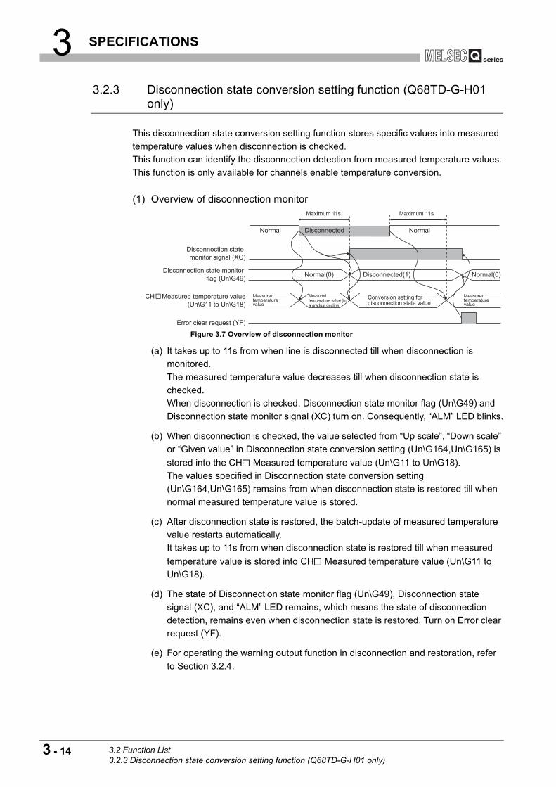
3 SPECIFICATIONS
3.2.3 Disconnection state conversion setting function (Q68TD-G-H01 only)
This disconnection state conversion setting function stores specific values into measured
temperature values when disconnection is checked.
This function can identify the disconnection detection from measured temperature values.
This function is only available for channels enable temperature conversion.
(1) Overview of disconnection monitor
Figure 3.7 Overview of disconnection monitor
(a) It takes up to 11s from when line is disconnected till when disconnection is
monitored.
The measured temperature value decreases till when disconnection state is
checked.
When disconnection is checked, Disconnection state monitor flag (Un\G49) and
Disconnection state monitor signal (XC) turn on. Consequently, “ALM” LED blinks.
(b) When disconnection is checked, the value selected from “Up scale”, “Down scale”
or “Given value” in Disconnection state conversion setting (Un\G164,Un\G165) is
stored into the CH Measured temperature value (Un\G11 to Un\G18).
The values specified in Disconnection state conversion setting
(Un\G164,Un\G165) remains from when disconnection state is restored till when
normal measured temperature value is stored.
(c) After disconnection state is restored, the batch-update of measured temperature
value restarts automatically.
It takes up to 11s from when disconnection state is restored till when measured
temperature value is stored into CH Measured temperature value (Un\G11 to
Un\G18).
(d) The state of Disconnection state monitor flag (Un\G49), Disconnection state
signal (XC), and “ALM” LED remains, which means the state of disconnection
detection, remains even when disconnection state is restored. Turn on Error clear
request (YF).
(e) For operating the warning output function in disconnection and restoration, refer
to Section 3.2.4.
Normal Normal
Measured temperature value
Measured temperature value
Normal(0) Normal(0)Disconnected(1)
Disconnected
CH Measured temperature value
(Un\G11 to Un\G18)
Maximum 11s Maximum 11s
Conversion setting for disconnection state value
Disconnection state
monitor signal (XC)
Disconnection state monitor
flag (Un\G49)
Measured temperature value (in a gradual decline)
Error clear request (YF)
3 - 14 3.2 Function List3.2.3 Disconnection state conversion setting function (Q68TD-G-H01 only)

3 SPECIFICATIONS
1
OV
ER
VIE
W
2
SY
ST
EM
C
ON
FIG
UR
AT
ION
3
SP
EC
IFIC
AT
ION
S
4
SE
TU
P A
ND
P
RO
CE
DU
RE
S B
EF
OR
E
OP
ER
AT
ION
5
UT
ILIT
Y P
AC
KA
GE
(G
X
CO
NF
IGU
RA
TO
R-T
I)
6
PR
OG
RA
MM
ING
7
ON
LIN
E M
OD
ULE
C
HA
NG
E
8
TR
OU
BL
ES
HO
OT
ING
(2) Setting methodsWhen “Up scale”, “Down scale” or “Given value” is selected in Disconnection state
conversion setting (Un\G164,Un\G165), the value to be stored into the CH
Measured temperature value (Un\G11 to Un\G18) in disconnection check can be
specified.
(a) Up-scale and down-scale
When “Up scale” (0H) or “Down scale” (1H) is selected, an up-scale value or
down-scale value of thermocouple-type to be used is stored into the CH
Measured temperature value (Un\G11 to Un\G18).
(b) Given value
When “Given value” (2H) is selected, set a value in the CH CH1 Conversion
setting value for disconnection state (Un\G166 to Un\G173) in units of 0.1 .
The value set in the buffer memory above is stored in the CH Measured
temperature value (Un\G11 to Un\G18) during disconnection state.
Table 3.5 Up-scale and down-scale list
Thermocouple
typeSetting value
Measurement
range
Measured temperature value when
disconnection is detected
Up scale Down scale
Thermocouple K 0 -270 to 1370 1452.0 -352.0
Thermocouple E 1 -270 to 1000 1063.5 -333.5
Thermocouple J 2 -210 to 1200 1270.5 -280.5
Thermocouple T 3 -270 to 400 433.5 -303.5
Thermocouple B 4 0 to 1820 1911.0 -91.0
Thermocouple R 5 -50 to 1760 1850.5 -140.5
Thermocouple S 6 -50 to 1760 1850.5 -140.5
Thermocouple N 7 -270 to 1300 1378.5 -348.5
3.2 Function List3.2.3 Disconnection state conversion setting function (Q68TD-G-H01 only)
3 - 15

3 SPECIFICATIONS
3.2.4 Warning output function
(1) Process alarm
(a) Warning occurrence
When the detected measured temperature value is higher than or equal to the
process alarm upper upper limit value or lower than or equal to the process alarm
lower lower limit value and falls in the warning output range, a warning occurs.
When a warning occurs, it is notified by storing "1" in the bit position
corresponding to the channel of the warning output flag (process alarm)(Un\G47),
and turning ON the warning output signal (XD) and the [ALM] LED.
(b) Warning clearance
After a warning occurrence, when the temperature value falls lower than the
process alarm upper lower limit value or rises higher than the process alarm lower
upper limit value and returns to within the setting range, the warning is cleared.
When the warning is cleared, "0" is stored in the bit position corresponding to the
channel of the warning output flag (process alarm)(Un\G47).
The warning output signal (XD) turns OFF and the "ALM" LED turns off only when
the process alarm and rate alarm warnings for all channels do not occur or are in
clearance state.
Figure 3.8 Warning output occurence and clearance (Process alarm)
Warning output range section
Out of warning output range section
Included
Time
Warning clearance
Warning clearance
Temperature
Upper upperlimit value
Upper lowerlimit value
CH1 measuredtemperature value
Lower upperlimit value
CH2 measured temperature value
Lower lowerlimit value
Warning occurence
Warning occurence
Warning clearance
Warning clearance
CH1 Process alarm upper
limit value (Un\G47.b0)
CH1 Process alarm lower
limit value (Un\G47.b1)
CH2 Process alarm upper
limit value (Un\G47.b2)
Warning output signal (XD)
3 - 16 3.2 Function List3.2.4 Warning output function

3 SPECIFICATIONS
1
OV
ER
VIE
W
2
SY
ST
EM
C
ON
FIG
UR
AT
ION
3
SP
EC
IFIC
AT
ION
S
4
SE
TU
P A
ND
P
RO
CE
DU
RE
S B
EF
OR
E
OP
ER
AT
ION
5
UT
ILIT
Y P
AC
KA
GE
(G
X
CO
NF
IGU
RA
TO
R-T
I)
6
PR
OG
RA
MM
ING
7
ON
LIN
E M
OD
ULE
C
HA
NG
E
8
TR
OU
BL
ES
HO
OT
ING
(c) Settable range and default value differ according to the thermocouple type.
Set it in unit of 0.1 .
(d) When time average or count average is specified, process-alarm processing is
executed for each preset time or count.
When other temperature conversion system (sampling processing, moving
average, or primary delay filter) is specified, process-alarm processing is
executed at every sampling time.
(e) When the value of the Conversion setting for disconnection detection
(Un\G164,Un\G165) or Disconnection state conversion setting
(Un\G164,Un\G165) is set for disconnection detection or disconnection check as
follows, a warning occur.
• The lower or equal value to the value set in the process alarm lower lower
limit is set.
• The higher or equal value to the value set in the process alarm upper upper
limit is set.
(2) Rate alarm
(a) Warning occurrence
When the measured temperature value is monitored at every rate alarm warning
detection period and the changed portion from the preceding value is larger than
or equal to the rate alarm upper limit value or smaller than or equal to the rate
alarm lower limit value, a warning occurs.
When a warning occurs, it is notified by storing "1" in the bit position
corresponding to the channel of the warning output flag (rate alarm)(Un\G48), and
turning ON the warning output signal (XD) and the [ALM] LED.
Table 3.6 Settable range and default value of process alarm
Thermocouple
type
Default value
Settable temperature range
(Accuracy guarantee range)
Process
alarm
lower
upper
limit
value
Process
alarm
lower
lower
limit
value
Process
alarm
upper
upper
limit
value
Process
alarm
upper
lower
limit
value
Thermocouple K -2000 12000 -2700 to 13700 (-2000 to 12000)
Thermocouple E -2000 9000 -2700 to 10000 (-2000 to 9000)
Thermocouple J -400 7500 -2100 to 12000 (-400 to 7500)
Thermocouple T -2000 3500 -2700 to 4000 (-2000 to 3500)
Thermocouple B 6000 17000 0 to 18200 (6000 to 17000)
Thermocouple R 0 16000 -500 to 17600 (0 to 16000)
Thermocouple S 0 16000 -500 to 17600 (0 to 16000)
Thermocouple N -2000 12500 -2700 to 13000 (-2000 to 12500)
3.2 Function List3.2.4 Warning output function
3 - 17

3 SPECIFICATIONS
(b) Warning clearance
After a warning occurrence, when the changed portion of the measured
temperature value falls lower than the rate alarm upper limit value or rises higher
than the rate alarm lower limit value, and returns to within the setting range, the
warning is cleared.
When the warning is cleared, "0" is stored in the bit position corresponding to the
channel of the warning output flag (rate alarm)(Un\G48).
The warning output signal (XD) turns OFF and the "ALM" LED turns off only when
the process alarm and rate alarm warings for all channels do not occur or are in
clearance state.
Figure 3.9 Warning output occurence and clearance (Rate alarm)
(c) Set the rate alarm upper limit/lower limit values in units of 0.1 for the measured
temperature range.
Setting range is -32768 to 32767 (-3276.8 to 3276.7 ).
Initial value is set to "0".
CH1 measured temperature value
CH2 measured temperature value
Time
Time
Rate alarm upper limit value
Rate alarm lower limit value
Change of CH1 measured temperature value
Change of CH2 measured temperature value
CH1 Rate alarm upper
limit value (Un\G48.b0)
CH1 Rate alarm lower
limit value (Un\G48.b1)
CH2 Rate alarm upper
limit value (Un\G48.b2)
Warning output signal (XD)
Change of measured temperature value ( C)
Measured temperature value
Rate alarm warning detection period
Rate alarm warning detection period
3 - 18 3.2 Function List3.2.4 Warning output function

3 SPECIFICATIONS
1
OV
ER
VIE
W
2
SY
ST
EM
C
ON
FIG
UR
AT
ION
3
SP
EC
IFIC
AT
ION
S
4
SE
TU
P A
ND
P
RO
CE
DU
RE
S B
EF
OR
E
OP
ER
AT
ION
5
UT
ILIT
Y P
AC
KA
GE
(G
X
CO
NF
IGU
RA
TO
R-T
I)
6
PR
OG
RA
MM
ING
7
ON
LIN
E M
OD
ULE
C
HA
NG
E
8
TR
OU
BL
ES
HO
OT
ING
(d) The rate alarm warning detection period is set based on the period batch-updating
measured temperature values and the number of the periods.
Setting range is 1 to 6000 (times).
Calculation method of the rate alarm warning detection period is below.
[Example 1: When setting the rate alarm warning detection period to 150 times with
sampling processing]
Rate alarm warning detection period = 150 times 320ms = 48000ms = 48s
[Example 2: When setting the rate alarm warning detection period to 150 times with
2000ms of time average for the averaging processing)]
2000 320 = 6.25 (times) Drop the fractional part
The batch-updated period of 2000ms of time average is same as the period of 1920ms
(320ms 6 times)
Rate alarm warning detection period = 150 times 1920ms=288000ms = 288s
[Example 3: When setting the rate alarm warning detection period to 150 times with 10
times of count average for the averaging processing]
Rate alarm warning detection period = 150 times 10 times 320ms = 480000ms =
480s
[Example 4: When setting the rate alarm warning detection period to 150 times with 4
times of moving average for the averaging processing)]
Rate alarm warning detection period = 150 times 320ms=48000ms = 48s
(e) Rate alarm is effective to monitor a change of measured temperature values
within a limited range.
1) Setting example of the rate alarm upper limit/lower limit values for monitoring
that a measured temperature value rises within the specified range
Figure 3.10 Setting example of rate alarm upper limit or lower limit
(Rate alarm warning detection period) =
(Setting value of the rate alarm warning detection period)
(Temperature measurement value update period)
Rate alarm upper limit value
Rate alarm lower limit value
20.0
10.0
0
C
C
Time
Change of measured temperature value ( C)
3.2 Function List3.2.4 Warning output function
3 - 19

3 SPECIFICATIONS
2) Setting example of rate alarm upper limit/lower limit values for monitoring that
a measured temperature value drops within the specified range
Figure 3.11 Setting example of rate alarm upper limit or lower limit
3) Setting example of rate alarm upper limit/lower limit values for monitoring that
a measured temperature value changes within the specified range
Figure 3.12 Setting example of rate alarm upper limit or lower limit
(f) When the value of the Conversion setting for disconnection detection
(Un\G164,Un\G165) or Disconnection state conversion setting
(Un\G164,Un\G165) is set for disconnection detection or disconnection check as
follows, a warning occur.
• The changed portion from the preceding value is smaller than or equal to the
rate alarm lower limit value.
• The changed portion from the preceding value is larger than or equal to the
rate alarm upper limit value.
(g) After connection is restored, preceding values required for rate alarm occurence
are cleared.
Therefore, a warning does not occur even though the changed portion of
measured temperature values before and after temperature conversion exceeds
the setting range when temperature conversion is restarted.
Change of measured temperature value ( C)
Rate alarm upper limit value
Rate alarm lower limit value
Time
0
-10.0 C
-20.0 C
Change of measured temperature value ( C)
0
-10.0 C
10.0 C
Rate alarm upper limit value
Rate alarm lower limit value
Time
3 - 20 3.2 Function List3.2.4 Warning output function
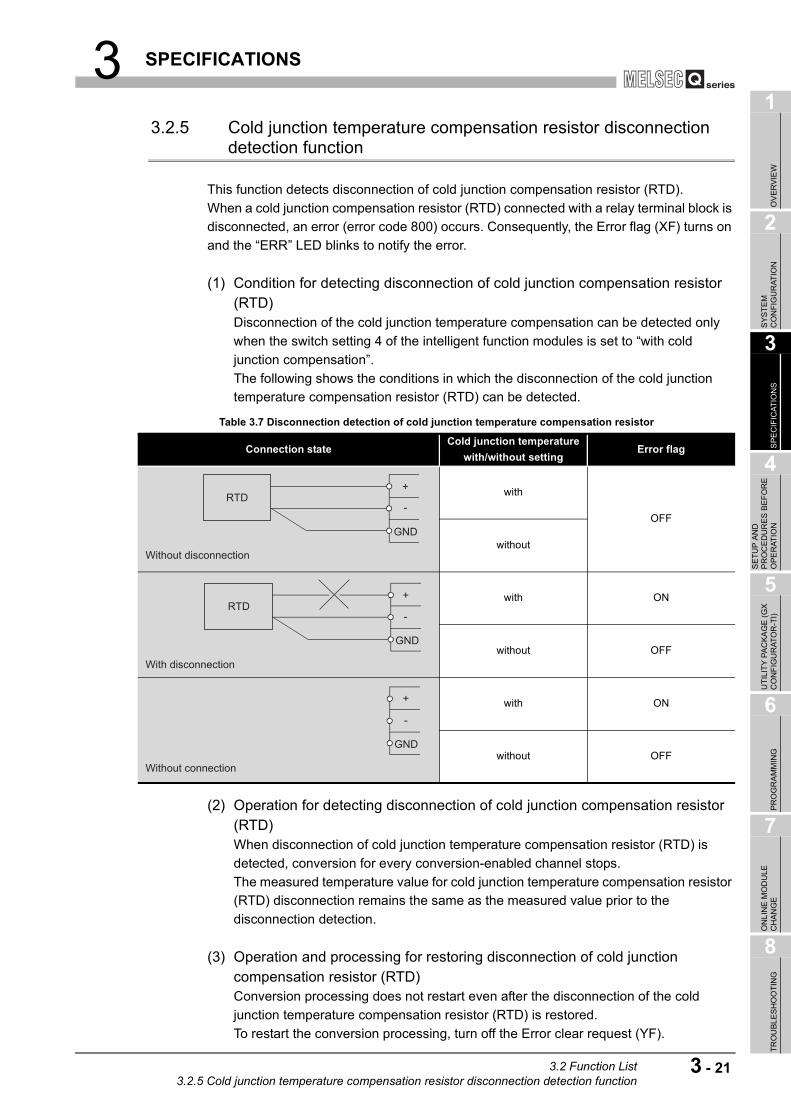
3 SPECIFICATIONS
1
OV
ER
VIE
W
2
SY
ST
EM
C
ON
FIG
UR
AT
ION
3
SP
EC
IFIC
AT
ION
S
4
SE
TU
P A
ND
P
RO
CE
DU
RE
S B
EF
OR
E
OP
ER
AT
ION
5
UT
ILIT
Y P
AC
KA
GE
(G
X
CO
NF
IGU
RA
TO
R-T
I)
6
PR
OG
RA
MM
ING
7
ON
LIN
E M
OD
ULE
C
HA
NG
E
8
TR
OU
BL
ES
HO
OT
ING
3.2.5 Cold junction temperature compensation resistor disconnection detection function
This function detects disconnection of cold junction compensation resistor (RTD).
When a cold junction compensation resistor (RTD) connected with a relay terminal block is
disconnected, an error (error code 800) occurs. Consequently, the Error flag (XF) turns on
and the “ERR” LED blinks to notify the error.
(1) Condition for detecting disconnection of cold junction compensation resistor (RTD)Disconnection of the cold junction temperature compensation can be detected only
when the switch setting 4 of the intelligent function modules is set to “with cold
junction compensation”.
The following shows the conditions in which the disconnection of the cold junction
temperature compensation resistor (RTD) can be detected.
(2) Operation for detecting disconnection of cold junction compensation resistor (RTD)When disconnection of cold junction temperature compensation resistor (RTD) is
detected, conversion for every conversion-enabled channel stops.
The measured temperature value for cold junction temperature compensation resistor
(RTD) disconnection remains the same as the measured value prior to the
disconnection detection.
(3) Operation and processing for restoring disconnection of cold junction compensation resistor (RTD)Conversion processing does not restart even after the disconnection of the cold
junction temperature compensation resistor (RTD) is restored.
To restart the conversion processing, turn off the Error clear request (YF).
Table 3.7 Disconnection detection of cold junction temperature compensation resistor
Connection stateCold junction temperature
with/without settingError flag
with
OFF
without
with ON
without OFF
with ON
without OFF
GND
RTD
Without disconnection
+
-
GND
RTD
With disconnection
+
-
GND
Without connection
+
-
3.2 Function List3.2.5 Cold junction temperature compensation resistor disconnection detection function
3 - 21

3 SPECIFICATIONS
3.3 I/O Signals Transferred to/from Programmable Controller CPU
This section describes the I/O signal assignment and signal functions.
3.3.1 I/O signal list
The following are the I/O signals of the Q68TD-G-H02 (H01).
The I/O numbers (X/Y) given in this chapter and later assume that the first I/O number of
the Q68TD-G-H02 (H01) is set to 0.
POINTThe reserved signals marked *1 are used by the system and are unavailable for
the user. Should they be turned on/off in a sequence program, we cannot
guarantee the functions of the Q68TD-G-H02 (H01).
Table 3.8 I/O signal list
Input signal
(Signal direction:
Programmable controller CPU Q68TD-G-H02 (H01))
Output signal
(Signal direction:
Programmable controller CPU Q68TD-G-H02 (H01))
Device No. Signal name Device No. Signal name
X0 Module ready Y0
Reserved *1
X1
Reserved *1
Y1
X2 Y2
X3 Y3
X4 Y4
X5 Y5
X6 Y6
X7 Y7
X8 Y8
X9 Operating condition setting completion flag Y9 Operating condition setting request
XA Offset/gain setting mode status flag YA User range write request
XB Channel change completion flag YB Channel change request
XC
Disconnection detection signal (Q68TD-G-H02 only)
YC
Reserved *1Disconnection state monitor signal (Q68TD-G-H01
only)
XD Warning output signal YD
XE Conversion completion flag YE
XF Error flag YF Error clear request
3 - 22 3.3 I/O Signals Transferred to/from Programmable Controller CPU3.3.1 I/O signal list

3 SPECIFICATIONS
1
OV
ER
VIE
W
2
SY
ST
EM
C
ON
FIG
UR
AT
ION
3
SP
EC
IFIC
AT
ION
S
4
SE
TU
P A
ND
P
RO
CE
DU
RE
S B
EF
OR
E
OP
ER
AT
ION
5
UT
ILIT
Y P
AC
KA
GE
(G
X
CO
NF
IGU
RA
TO
R-T
I)
6
PR
OG
RA
MM
ING
7
ON
LIN
E M
OD
ULE
C
HA
NG
E
8
TR
OU
BL
ES
HO
OT
ING
3.3.2 I/O signal details
The following are details of the Q68TD-G-H02 (H01) I/O signals.
(1) Module ready (X0)
(a) If the module is in the normal mode at power-on or resetting of the programmable
controller CPU, this signal turns on to start conversion processing as soon as it
gets ready for conversion.
(b) When this signal (X0) is off in the normal mode, conversion processing is not
performed. In the offset/gain setting mode, conversion processing is performed if
this signal (X0) is off.
(c) This signal (X0) turns off when:
• The module is in the offset/gain setting mode
• The Q68TD-G-H02 (H01) is in a watchdog timer error *1 * 1 Occurs if program operation is not completed within the intended time due to errors such as a
hardware fault of the Q68TD-G-H02 (H01). The RUN LED of the Q68TD-G-H02 (H01) goes off when a watchdog timer error occurs.
(2) Operation condition setting completion flag (X9)
(a) When the following settings are changed, this signal is used as an interlock
condition to turn ON/OFF the operation condition setting request (Y9).
• Conversion enable/disable setting (Un\G0)
• CH Time/Count/Moving average/Time constant setting (Un\G1 to Un\G8)
• Averaging processing selection (Un\G24,Un\G25)
• Warning output enable/disable setting (Un\G46)
• Scaling valid/invalid setting (Un\G58)
• CH Scaling range upper/lower limit value (Un\G62 to Un\G77)
• CH Scaling width upper/lower limit value (Un\G78 to Un\G93)
• CH Process alarm upper/lower limit value (Un\G94 to Un\G125)
• CH Rate alarm warning detection period (Un\126 to Un\G133)
• CH Rate alarm upper/lower limit value (Un\G134 to Un\G149)
• Conversion setting for disconnection detection (Un\G164,Un\G165) (Q68TD-
G-H02 only)
• Disconnection state conversion setting (Un\G164,Un\G165) (Q68TD-G-H01
only)
• CH Conversion setting value for disconnection detection (Un\G166 to
Un\G173) (Q68TD-G-H02 only)
• CH Conversion setting value for disconnection state (Un\G166 to Un\G173)
(Q68TD-G-H01 only)
When Operation condition setting completion flag (X9) is OFF, conversion processing
is not carried out.
3.3 I/O Signals Transferred to/from Programmable Controller CPU3.3.2 I/O signal details
3 - 23

3 SPECIFICATIONS
(b) Operating condition setting completion flag (X9) turns OFF in the following status.
• When Operating condition setting request (Y9) is ON.
Figure 3.13 When Operating condition setting request (Y9) is ON
(3) Offset/gain setting mode status flag (XA)
(a) In offset/gain setting mode
1) This signal is used as an interlock condition to turn ON/OFF the user range
write request (YA) when the value at completion of offset/gain setting
adjustment is registered.
2) See Section 4.6 regarding the offset/gain settings.
Figure 3.14 Offset/gain setting mode status flag (XA) during offset/gain setting mode
(b) In normal mode
1) This signal is used as an interlock condition to turn ON/OFF the user range
write request (YA) when the user range is restored.
2) Refer to CHAPTER 7 for the user range restoration.
Figure 3.15 Offset/gain setting mode status flag (XA) during normal mode
Module ready (X0)
Operating condition
setting completion flag (X9)
Operating condition setting
request (Y9)
Conversion enable/disable
setting (Un\G0)
Conversion completion
flag (XE)
Conversion disabled
Conversion enabled
Executed in Q68TD-G-H02(H01)Executed in sequence program
Module ready (X0)OFF
Offset/gain setting mode
status flag (XA)
User range write request (YA)
Executed in Q68TD-G-H02(H01)
Executed in sequence program
Module ready (X0)ON
Offset/gain setting mode status
flag (XA)
User range write request (YA)
Executed in Q68TD-G-H02(H01)
Executed in sequence program
3 - 24 3.3 I/O Signals Transferred to/from Programmable Controller CPU3.3.2 I/O signal details

3 SPECIFICATIONS
1
OV
ER
VIE
W
2
SY
ST
EM
C
ON
FIG
UR
AT
ION
3
SP
EC
IFIC
AT
ION
S
4
SE
TU
P A
ND
P
RO
CE
DU
RE
S B
EF
OR
E
OP
ER
AT
ION
5
UT
ILIT
Y P
AC
KA
GE
(G
X
CO
NF
IGU
RA
TO
R-T
I)
6
PR
OG
RA
MM
ING
7
ON
LIN
E M
OD
ULE
C
HA
NG
E
8
TR
OU
BL
ES
HO
OT
ING
(4) Channel change completion flag (XB)
(a) This signal is used as an interlock condition to turn ON/OFF the channel change
request (YB) when changing the channel for the offset/gain setting.
(b) For offset/gain setting, refer to Section 4.6.
Figure 3.16 Channel change completion flag (XB)
(5) Disconnection detection signal (XC) (Q68TD-G-H02 only)
(a) This signal turns on when any input signal line including a thermocouple in the
input circuit of the conversion-enabled channel is disconnected.
To identify the disconnected channel, check Disconnection detection flag
(Un\G49).
When this signal turns on, conversion update for the conversion-enabled
channels stops.
(b) Measured temperature value when this signal turns on can be selected from "Up
scale", "Down scale", or "Given scale". (Refer to Section 3.2.2)
(c) This signal turns off after eliminating the cause of disconnection and turning on
Error clear request (YF).
(d) When connection is restored, the measured temperature value update is restarted
regardless of the reset of this signal.
(6) Disconnection state monitor signal (XC) (Q68TD-G-H01 only)
(a) The thermocouple input circuit of the conversion-enabled channel turns ON the
disconnection state monitor signal (XC) when any input signal line including the
thermocouple is disconnected.
To identify the disconnected channel, check with the disconnection state monitor
flag (Un\G49).
In addition, conversion update for the conversion-enabled channels stops.
(b) For measured temperature values to be stored when the disconnection state
monitor signal (XC) turns ON, any of "Up scale", "Down scale", or "Given value"
can be selected (refer to Section 3.2.3).
(c) Removing the cause of disconnection and turning ON the error clear request (YF)
turns OFF the disconnection state monitor signal (XC).
(d) When the line connection is recovered, the temperature conversion value update
is restarted regardless of the disconnection state monitor signal (XC) reset.
Offset/gain setting mode
offset/gain specification
(Un\G26, Un\G27)
Channel change completion
flag (XB)
Channel change request (YB)
Executed in Q68TD-G-H02(H01)
Executed in sequence program
3.3 I/O Signals Transferred to/from Programmable Controller CPU3.3.2 I/O signal details
3 - 25

3 SPECIFICATIONS
(7) Warning output signal (XD)
(a) The warning output signal (XD) turns ON when a process alarm or rate alarm is
detected.
1) Process alarm
• This signal turns ON when the process alarm is enabled and a measured
temperature value exceeds the preset range of the process alarm upper/
lower limit value (Un\G94 to Un\G125) in a conversion-enabled channel.
• For every conversion-enabled channel, the signal automatically turns OFF
when the measured temperature value returns to within the setting range,
and the "ALM" LED also turns off.
2) Rate alarm
• This signal turns ON when the rate alarm is enabled and the change of
measured temperature value exceeds the preset range of the rate alarm
upper/lower limit value (Un\G134 to Un\G149) in a conversion-enabled
channel.
• For every conversion-enabled channel, the signal automatically turns OFF
when the change of measured temperature values return to within the
setting range, and the "ALM" LED also turns off.
Figure 3.17 On or off for warning output signal (XD)
Executed in Q68TD-G-H02(H01)
Warning output flag
(Un\G47, Un\G48)
Warning output
signal (XD)
0 0Warning occurrence (process alarm, rate alarm)
3 - 26 3.3 I/O Signals Transferred to/from Programmable Controller CPU3.3.2 I/O signal details

3 SPECIFICATIONS
1
OV
ER
VIE
W
2
SY
ST
EM
C
ON
FIG
UR
AT
ION
3
SP
EC
IFIC
AT
ION
S
4
SE
TU
P A
ND
P
RO
CE
DU
RE
S B
EF
OR
E
OP
ER
AT
ION
5
UT
ILIT
Y P
AC
KA
GE
(G
X
CO
NF
IGU
RA
TO
R-T
I)
6
PR
OG
RA
MM
ING
7
ON
LIN
E M
OD
ULE
C
HA
NG
E
8
TR
OU
BL
ES
HO
OT
ING
(8) Conversion completion flag (XE)
(a) Conversion completion flag (XE) turns ON when the measured temperature
values of all conversion-enabled channels are stored into buffer memory after
power-on or hardware reset.
(b) When averaging processing is performed, this signal also turns ON when the
converted measured temperature value is stored into buffer memory after
completion of averaging processing.
(c) When Operating condition setting completion flag (X9) turns on (stop
conversion)
1) After the measured temperature value is stored into buffer memory, the bit of
corresponding channel in Conversion completion flag (Un\G10) turns on
(changes to "1").
2) After the measured temperature values of all conversion-enabled channels are
stored into buffer memory, this flag turns on.
(d) When Operating condition setting completion flag (X9) turns off (conversion
stop)
1) The bits of all channels in Conversion completion flag (Un\G10) are turned off
(changes to "0").
2) This flag (XE) turns off.
Note that even though conversion has been stopped, the data immediately
before the stop are held in the Measured temperature values stored in the
buffer memory.
(e) Use this signal or Conversion completion flag (Un\G10) as an interlock to read out
the measured temperature value.
(f) This flag (XE) does not turn on when all channels are set to conversion-disabled.
(9) Error Flag (XF)
(a) Error flag (XF) turns ON when a writing error occurs.
(b) To clear the error code, turn ON Error clear request (YF).
Figure 3.18 On or off for Error flag (XF)
Error code (Un\G19)
Error flag (XF)
Error clear request (YF)
Error occurrence
Executed in Q68TD-G-H02(H01)
Executed in sequence program
3.3 I/O Signals Transferred to/from Programmable Controller CPU3.3.2 I/O signal details
3 - 27

3 SPECIFICATIONS
(10)Operating condition setting request (Y9)
(a) This signal is turned ON when enabling the following setting contents.
• Conversion enable/disable setting (Un\G0)
• CH Time/Count/Moving average/Time constant setting (Un\G1 to Un\G8)
• Averaging processing selection (Un\G24,Un\G25)
• Warning output enable/disable setting (Un\G46)
• Scaling valid/invalid setting (Un\G58)
• CH Scaling range upper/lower limit value (Un\G62 to Un\G77)
• CH Scaling width upper/lower limit value (Un\G78 to Un\G93)
• CH Process alarm upper/lower limit value (Un\G94 to Un\G125)
• CH Rate alarm warning detection period (Un\G126 to Un\G133)
• CH Rate alarm upper/lower limit value (Un\G134 to Un\G149)
• Conversion setting for disconnection detection (Un\G164,Un\G165) (Q68TD-
G-H02 only)
• Disconnection state conversion setting (Un\G164,Un\G165) (Q68TD-G-H01
only)
• CH Conversion setting value for disconnection detection (Un\G166 to
Un\G173) (Q68TD-G-H02 only)
• CH Conversion setting value for disconnection state (Un\G166 to
Un\G173) (Q68TD-G-H01 only)
(b) When this signal is turned on, Disconnection detection signal (XC) and Warning
output signal (XD) turn off.
(c) For the ON/OFF timing, refer to the field of the operating condition setting
completion flag (X9).
(11)User range write request (YA)
(a) In offset/gain setting mode
1) This signal turns ON when registering the adjusted value of offset/gain setting
to the flash memory.
2) For the ON/OFF timing, refer to the field of the offset/gain setting mode status
flag (XA).
For offset/gain settings, refer to Section 4.6.
(b) In normal mode
1) This signal turns ON when the user range is restored.
2) For the ON/OFF timing, refer to the field of the offset/gain setting mode status
flag (XA).
For user range restoration, refer to CHAPTER 7.
3 - 28 3.3 I/O Signals Transferred to/from Programmable Controller CPU3.3.2 I/O signal details

3 SPECIFICATIONS
1
OV
ER
VIE
W
2
SY
ST
EM
C
ON
FIG
UR
AT
ION
3
SP
EC
IFIC
AT
ION
S
4
SE
TU
P A
ND
P
RO
CE
DU
RE
S B
EF
OR
E
OP
ER
AT
ION
5
UT
ILIT
Y P
AC
KA
GE
(G
X
CO
NF
IGU
RA
TO
R-T
I)
6
PR
OG
RA
MM
ING
7
ON
LIN
E M
OD
ULE
C
HA
NG
E
8
TR
OU
BL
ES
HO
OT
ING
(12)Channel change request (YB)
(a) This signal turns ON when changing the channel for executing the offset/gain
setting.
(b) For the ON/OFF timing, refer to the field of the channel change completion flag
(XB).
For the offset/gain setting, refer to Section 4.6.
(13)Error clear request (YF)
(a) This signal turns ON when clearing Error flag (XF) and Disconnection state
monitor signal (XC).
However, the setting value error of the intelligent function module switch setting
cannot be cleared.
Correct the setting value.
(b) For the ON/OFF timing, refer to the filed of Disconnection state monitor signal
(XC) and Error flag (XF)
3.3 I/O Signals Transferred to/from Programmable Controller CPU3.3.2 I/O signal details
3 - 29

3 SPECIFICATIONS
3.4 Buffer Memory
3.4.1 Buffer memory assignment
This section describes the assignment of the Q68TD-G-H02 (H01) buffer memory.
POINTDo not write data from system area or sequence program to the buffer memory area
where writing is disabled.
Doing so may cause malfunction.
Table 3.9 Buffer memory assignment
AddressesDescription Default value Read/Write*1
Reference
sectionHex. Dec.
00H 0 Conversion enable/disable setting 00FFH R/W*2 Section 3.4.2
01H 1 CH1 Time/Count/Moving average/Time constant setting 0 R/W*2
Section 3.4.3
02H 2 CH2 Time/Count/Moving average/Time constant setting 0 R/W*2
03H 3 CH3 Time/Count/Moving average/Time constant setting 0 R/W*2
04H 4 CH4 Time/Count/Moving average/Time constant setting 0 R/W*2
05H 5 CH5 Time/Count/Moving average/Time constant setting 0 R/W*2
06H 6 CH6 Time/Count/Moving average/Time constant setting 0 R/W*2
07H 7 CH7 Time/Count/Moving average/Time constant setting 0 R/W*2
08H 8 CH8 Time/Count/Moving average/Time constant setting 0 R/W*2
09H 9 System area - - -
0AH 10 Conversion completion flag 0 R Section 3.4.4
0BH 11 CH1 Measured temperature value 0 R
Section 3.4.5
0CH 12 CH2 Measured temperature value 0 R
0DH 13 CH3 Measured temperature value 0 R
0EH 14 CH4 Measured temperature value 0 R
0FH 15 CH5 Measured temperature value 0 R
10H 16 CH6 Measured temperature value 0 R
11H 17 CH7 Measured temperature value 0 R
12H 18 CH8 Measured temperature value 0 R
13H 19 Error code 0 R Section 3.4.6
14H 20 Setting range 1(Thermocouple type CH1-CH4) 0 RSection 3.4.7
15H 21 Setting range 2(Thermocouple type CH5-CH8) 0 R
16H 22 Setting range 3(Offset/gain setting CH1-CH8) 0 R Section 3.4.8
17H 23 System area - - -
18H 24 Averaging processing selection (CH1-CH4) 0 R/W*2
Section 3.4.919H 25 Averaging processing selection (CH5-CH8) 0 R/W*2
1AH 26 Offset/gain setting mode(Offset specification) 0 R/W*2
Section 3.4.101BH 27 Offset/gain setting mode(Gain specification) 0 R/W*2
3 - 30 3.4 Buffer Memory3.4.1 Buffer memory assignment

3 SPECIFICATIONS
1
OV
ER
VIE
W
2
SY
ST
EM
C
ON
FIG
UR
AT
ION
3
SP
EC
IFIC
AT
ION
S
4
SE
TU
P A
ND
P
RO
CE
DU
RE
S B
EF
OR
E
OP
ER
AT
ION
5
UT
ILIT
Y P
AC
KA
GE
(G
X
CO
NF
IGU
RA
TO
R-T
I)
6
PR
OG
RA
MM
ING
7
ON
LIN
E M
OD
ULE
C
HA
NG
E
8
TR
OU
BL
ES
HO
OT
ING
1CH 28 CH1 Offset temperature setting value 0 R/W*2
Section 3.4.11
1DH 29 CH1 Gain temperature setting value 0 R/W*2
1EH 30 CH2 Offset temperature setting value 0 R/W*2
1FH 31 CH2 Gain temperature setting value 0 R/W*2
20H 32 CH3 Offset temperature setting value 0 R/W*2
21H 33 CH3 Gain temperature setting value 0 R/W*2
22H 34 CH4 Offset temperature setting value 0 R/W*2
23H 35 CH4 Gain temperature setting value 0 R/W*2
24H 36 CH5 Offset temperature setting value 0 R/W*2
25H 37 CH5 Gain temperature setting value 0 R/W*2
26H 38 CH6 Offset temperature setting value 0 R/W*2
27H 39 CH6 Gain temperature setting value 0 R/W*2
28H 40 CH7 Offset temperature setting value 0 R/W*2
29H 41 CH7 Gain temperature setting value 0 R/W*2
2AH 42 CH8 Offset temperature setting value 0 R/W*2
2BH 43 CH8 Gain temperature setting value 0 R/W*2
2CH 44 System area - - -
2DH 45Cold junction compensation setting state (Q68TD-G-H02 only) 0 R Section 3.4.12
System area (Q68TD-G-H01 only) - - -
2EH 46 Warning output enable/disable setting FFFFH R/W*2 Section 3.4.13
2FH 47 Warning output flag(Process alarm) 0 RSection 3.4.14
30H 48 Warning output flag(Rate alarm) 0 R
31H 49Disconnection detection flag (Q68TD-G-H02 only)
0 RSection 3.4.15
Disconnection state monitor flag (Q68TD-G-H01 only) Section 3.4.16
32H 50 CH1 Scaling value 0 R
Section 3.4.17
33H 51 CH2 Scaling value 0 R
34H 52 CH3 Scaling value 0 R
35H 53 CH4 Scaling value 0 R
36H 54 CH5 Scaling value 0 R
37H 55 CH6 Scaling value 0 R
38H 56 CH7 Scaling value 0 R
39H 57 CH8 Scaling value 0 R
3AH 58 Scaling valid/invalid setting 00FFH R/W*2 Section 3.4.18
3BH 59
System area - - -to to
3DH 61
Table 3.9 Buffer memory assignment
AddressesDescription Default value Read/Write*1
Reference
sectionHex. Dec.
3.4 Buffer Memory3.4.1 Buffer memory assignment
3 - 31

3 SPECIFICATIONS
3EH 62 CH1 Scaling range lower limit value 0 R/W*2
Section 3.4.19
3FH 63 CH1 Scaling range upper limit value 0 R/W*2
40H 64 CH2 Scaling range lower limit value 0 R/W*2
41H 65 CH2 Scaling range upper limit value 0 R/W*2
42H 66 CH3 Scaling range lower limit value 0 R/W*2
43H 67 CH3 Scaling range upper limit value 0 R/W*2
44H 68 CH4 Scaling range lower limit value 0 R/W*2
45H 69 CH4 Scaling range upper limit value 0 R/W*2
46H 70 CH5 Scaling range lower limit value 0 R/W*2
47H 71 CH5 Scaling range upper limit value 0 R/W*2
48H 72 CH6 Scaling range lower limit value 0 R/W*2
49H 73 CH6 Scaling range upper limit value 0 R/W*2
4AH 74 CH7 Scaling range lower limit value 0 R/W*2
4BH 75 CH7 Scaling range upper limit value 0 R/W*2
4CH 76 CH8 Scaling range lower limit value 0 R/W*2
4DH 77 CH8 Scaling range upper limit value 0 R/W*2
4EH 78 CH1 Scaling width lower limit value 0 R/W*2
Section 3.4.20
4FH 79 CH1 Scaling width upper limit value 0 R/W*2
50H 80 CH2 Scaling width lower limit value 0 R/W*2
51H 81 CH2 Scaling width upper limit value 0 R/W*2
52H 82 CH3 Scaling width lower limit value 0 R/W*2
53H 83 CH3 Scaling width upper limit value 0 R/W*2
54H 84 CH4 Scaling width lower limit value 0 R/W*2
55H 85 CH4 Scaling width upper limit value 0 R/W*2
56H 86 CH5 Scaling width lower limit value 0 R/W*2
57H 87 CH5 Scaling width upper limit value 0 R/W*2
58H 88 CH6 Scaling width lower limit value 0 R/W*2
59H 89 CH6 Scaling width upper limit value 0 R/W*2
5AH 90 CH7 Scaling width lower limit value 0 R/W*2
5BH 91 CH7 Scaling width upper limit value 0 R/W*2
5CH 92 CH8 Scaling width lower limit value 0 R/W*2
5DH 93 CH8 Scaling width upper limit value 0 R/W*2
Table 3.9 Buffer memory assignment
AddressesDescription Default value Read/Write*1
Reference
sectionHex. Dec.
3 - 32 3.4 Buffer Memory3.4.1 Buffer memory assignment

3 SPECIFICATIONS
1
OV
ER
VIE
W
2
SY
ST
EM
C
ON
FIG
UR
AT
ION
3
SP
EC
IFIC
AT
ION
S
4
SE
TU
P A
ND
P
RO
CE
DU
RE
S B
EF
OR
E
OP
ER
AT
ION
5
UT
ILIT
Y P
AC
KA
GE
(G
X
CO
NF
IGU
RA
TO
R-T
I)
6
PR
OG
RA
MM
ING
7
ON
LIN
E M
OD
ULE
C
HA
NG
E
8
TR
OU
BL
ES
HO
OT
ING
5EH 94 CH1 Process alarm lower lower limit value -2000 R/W*2
Section 3.4.21
5FH 95 CH1 Process alarm lower upper limit value -2000 R/W*2
60H 96 CH1 Process alarm upper lower limit value 12000 R/W*2
61H 97 CH1 Process alarm upper upper limit value 12000 R/W*2
62H 98 CH2 Process alarm lower lower limit value -2000 R/W*2
63H 99 CH2 Process alarm lower upper limit value -2000 R/W*2
64H 100 CH2 Process alarm upper lower limit value 12000 R/W*2
65H 101 CH2 Process alarm upper upper limit value 12000 R/W*2
66H 102 CH3 Process alarm lower lower limit value -2000 R/W*2
67H 103 CH3 Process alarm lower upper limit value -2000 R/W*2
68H 104 CH3 Process alarm upper lower limit value 12000 R/W*2
69H 105 CH3 Process alarm upper upper limit value 12000 R/W*2
6AH 106 CH4 Process alarm lower lower limit value -2000 R/W*2
6BH 107 CH4 Process alarm lower upper limit value -2000 R/W*2
6CH 108 CH4 Process alarm upper lower limit value 12000 R/W*2
6DH 109 CH4 Process alarm upper upper limit value 12000 R/W*2
6EH 110 CH5 Process alarm lower lower limit value -2000 R/W*2
6FH 111 CH5 Process alarm lower upper limit value -2000 R/W*2
70H 112 CH5 Process alarm upper lower limit value 12000 R/W*2
71H 113 CH5 Process alarm upper upper limit value 12000 R/W*2
72H 114 CH6 Process alarm lower lower limit value -2000 R/W*2
73H 115 CH6 Process alarm lower upper limit value -2000 R/W*2
74H 116 CH6 Process alarm upper lower limit value 12000 R/W*2
75H 117 CH6 Process alarm upper upper limit value 12000 R/W*2
76H 118 CH7 Process alarm lower lower limit value -2000 R/W*2
77H 119 CH7 Process alarm lower upper limit value -2000 R/W*2
78H 120 CH7 Process alarm upper lower limit value 12000 R/W*2
79H 121 CH7 Process alarm upper upper limit value 12000 R/W*2
7AH 122 CH8 Process alarm lower lower limit value -2000 R/W*2
7BH 123 CH8 Process alarm lower upper limit value -2000 R/W*2
7CH 124 CH8 Process alarm upper lower limit value 12000 R/W*2
7DH 125 CH8 Process alarm upper upper limit value 12000 R/W*2
7EH 126 CH1 Rate alarm warning detection period 0 R/W*2
Section 3.4.22
7FH 127 CH2 Rate alarm warning detection period 0 R/W*2
80H 128 CH3 Rate alarm warning detection period 0 R/W*2
81H 129 CH4 Rate alarm warning detection period 0 R/W*2
82H 130 CH5 Rate alarm warning detection period 0 R/W*2
83H 131 CH6 Rate alarm warning detection period 0 R/W*2
84H 132 CH7 Rate alarm warning detection period 0 R/W*2
85H 133 CH8 Rate alarm warning detection period 0 R/W*2
Table 3.9 Buffer memory assignment
AddressesDescription Default value Read/Write*1
Reference
sectionHex. Dec.
3.4 Buffer Memory3.4.1 Buffer memory assignment
3 - 33

3 SPECIFICATIONS
86H 134 CH1 Rate alarm upper limit value 0 R/W*2
Section 3.4.23
87H 135 CH1 Rate alarm lower limit value 0 R/W*2
88H 136 CH2 Rate alarm upper limit value 0 R/W*2
89H 137 CH2 Rate alarm lower limit value 0 R/W*2
8AH 138 CH3 Rate alarm upper limit value 0 R/W*2
8BH 139 CH3 Rate alarm lower limit value 0 R/W*2
8CH 140 CH4 Rate alarm upper limit value 0 R/W*2
8DH 141 CH4 Rate alarm lower limit value 0 R/W*2
8EH 142 CH5 Rate alarm upper limit value 0 R/W*2
8FH 143 CH5 Rate alarm lower limit value 0 R/W*2
90H 144 CH6 Rate alarm upper limit value 0 R/W*2
91H 145 CH6 Rate alarm lower limit value 0 R/W*2
92H 146 CH7 Rate alarm upper limit value 0 R/W*2
93H 147 CH7 Rate alarm lower limit value 0 R/W*2
94H 148 CH8 Rate alarm upper limit value 0 R/W*2
95H 149 CH8 Rate alarm lower limit value 0 R/W*2
96H 150
System area - - -to to
9DH 157
9EH 158Mode switching setting 0 R/W*2 Section 3.4.24
9FH 159
A0H 160
System area - - -to to
A3H 163
A4H 164
Conversion setting for disconnection detection (CH1-
CH4)(Q68TD-G-H02 only)1111H R/W*2
Section 3.4.25
or
Section 3.4.26
Disconnection state conversion setting (CH1-CH4)(Q68TD-G-
H01 only)
A5H 165
Conversion setting for disconnection detection (CH5-
CH8)(Q68TD-G-H02 only)1111H R/W*2
Disconnection state conversion setting (CH5-CH8)(Q68TD-G-
H01 only)
Table 3.9 Buffer memory assignment
AddressesDescription Default value Read/Write*1
Reference
sectionHex. Dec.
3 - 34 3.4 Buffer Memory3.4.1 Buffer memory assignment

3 SPECIFICATIONS
1
OV
ER
VIE
W
2
SY
ST
EM
C
ON
FIG
UR
AT
ION
3
SP
EC
IFIC
AT
ION
S
4
SE
TU
P A
ND
P
RO
CE
DU
RE
S B
EF
OR
E
OP
ER
AT
ION
5
UT
ILIT
Y P
AC
KA
GE
(G
X
CO
NF
IGU
RA
TO
R-T
I)
6
PR
OG
RA
MM
ING
7
ON
LIN
E M
OD
ULE
C
HA
NG
E
8
TR
OU
BL
ES
HO
OT
ING
A6H 166
CH1 Conversion setting value for disconnection detection
(Q68TD-G-H02 only)0 R/W*2
Section 3.4.27
or
Section 3.4.28
CH1 Conversion setting value for disconnection state (Q68TD-
G-H01 only)
A7H 167
CH2 Conversion setting value for disconnection detection
(Q68TD-G-H02 only)0 R/W*2
CH2 Conversion setting value for disconnection state (Q68TD-G-
H01 only)
A8H 168
CH3 Conversion setting value for disconnection detection
(Q68TD-G-H02 only)0 R/W*2
CH3 Conversion setting value for disconnection state (Q68TD-G-
H01 only)
A9H 169
CH4 Conversion setting value for disconnection detection
(Q68TD-G-H02 only)0 R/W*2
CH4 Conversion setting value for disconnection state (Q68TD-G-
H01 only)
AAH 170
CH5 Conversion setting value for disconnection detection
(Q68TD-G-H02 only)0 R/W*2
CH5 Conversion setting value for disconnection state (Q68TD-G-
H01 only)
ABH 171
CH6 Conversion setting value for disconnection detection
(Q68TD-G-H02 only)0 R/W*2
CH6 Conversion setting value for disconnection state (Q68TD-G-
H01 only)
ACH 172
CH7 Conversion setting value for disconnection detection
(Q68TD-G-H02 only)0 R/W*2
CH7 Conversion setting value for disconnection state (Q68TD-G-
H01 only)
ADH 173
CH8 Conversion setting value for disconnection detection
(Q68TD-G-H02 only)0 R/W*2
CH8 Conversion setting value for disconnection state (Q68TD-G-
H01 only)
AEH 174
System area - - -to to
BDH 189
Table 3.9 Buffer memory assignment
AddressesDescription Default value Read/Write*1
Reference
sectionHex. Dec.
3.4 Buffer Memory3.4.1 Buffer memory assignment
3 - 35

3 SPECIFICATIONS
BEH 190 CH1 Factory default offset value*3 0 R/W*2
Section 3.4.29
BFH 191 CH1 Factory default gain value*3 0 R/W*2
C0H 192 CH1 User range settings offset value*3 0 R/W*2
C1H 193 CH1 User range settings gain value*3 0 R/W*2
C2H 194 CH1 User range settings thermal EMF offset value(L)*30 R/W*2
C3H 195 CH1 User range settings thermal EMF offset value(H)*3
C4H 196 CH1 User range settings thermal EMF gain value(L)*30 R/W*2
C5H 197 CH1 User range settings thermal EMF gain value(H)*3
C6H 198 CH2 Factory default offset value*3 0 R/W*2
C7H 199 CH2 Factory default gain value*3 0 R/W*2
C8H 200 CH2 User range settings offset value*3 0 R/W*2
C9H 201 CH2 User range settings gain value*3 0 R/W*2
CAH 202 CH2 User range settings thermal EMF offset value(L)*30 R/W*2
CBH 203 CH2 User range settings thermal EMF offset value(H)*3
CCH 204 CH2 User range settings thermal EMF gain value(L)*30 R/W*2
CDH 205 CH2 User range settings thermal EMF gain value(H)*3
CEH 206 CH3 Factory default offset value*3 0 R/W*2
CFH 207 CH3 Factory default gain value*3 0 R/W*2
D0H 208 CH3 User range settings offset value*3 0 R/W*2
D1H 209 CH3 User range settings gain value*3 0 R/W*2
D2H 210 CH3 User range settings thermal EMF offset value(L)*30 R/W*2
D3H 211 CH3 User range settings thermal EMF offset value(H)*3
D4H 212 CH3 User range settings thermal EMF gain value(L)*30 R/W*2
D5H 213 CH3 User range settings thermal EMF gain value(H)*3
D6H 214 CH4 Factory default offset value*3 0 R/W*2
D7H 215 CH4 Factory default gain value*3 0 R/W*2
D8H 216 CH4 User range settings offset value*3 0 R/W*2
D9H 217 CH4 User range settings gain value*3 0 R/W*2
DAH 218 CH4 User range settings thermal EMF offset value(L)*30 R/W*2
DBH 219 CH4 User range settings thermal EMF offset value(H)*3
DCH 220 CH4 User range settings thermal EMF gain value(L)*30 R/W*2
DDH 221 CH4 User range settings thermal EMF gain value(H)*3
DEH 222 CH5 Factory default offset value*3 0 R/W*2
DFH 223 CH5 Factory default gain value*3 0 R/W*2
E0H 224 CH5 User range settings offset value*3 0 R/W*2
E1H 225 CH5 User range settings gain value*3 0 R/W*2
E2H 226 CH5 User range settings thermal EMF offset value(L)*30 R/W*2
E3H 227 CH5 User range settings thermal EMF offset value(H)*3
E4H 228 CH5 User range settings thermal EMF gain value(L)*30 R/W*2
E5H 229 CH5 User range settings thermal EMF gain value(H)*3
E6H 230 CH6 Factory default offset value*3 0 R/W*2
E7H 231 CH6 Factory default gain value*3 0 R/W*2
E8H 232 CH6 User range settings offset value*3 0 R/W*2
E9H 233 CH6 User range settings gain value*3 0 R/W*2
EAH 234 CH6 User range settings thermal EMF offset value(L)*30 R/W*2
EBH 235 CH6 User range settings thermal EMF offset value(H)*3
ECH 236 CH6 User range settings thermal EMF gain value(L)*3 0 R/W*2
Table 3.9 Buffer memory assignment
AddressesDescription Default value Read/Write*1
Reference
sectionHex. Dec.
3 - 36 3.4 Buffer Memory3.4.1 Buffer memory assignment

3 SPECIFICATIONS
1
OV
ER
VIE
W
2
SY
ST
EM
C
ON
FIG
UR
AT
ION
3
SP
EC
IFIC
AT
ION
S
4
SE
TU
P A
ND
P
RO
CE
DU
RE
S B
EF
OR
E
OP
ER
AT
ION
5
UT
ILIT
Y P
AC
KA
GE
(G
X
CO
NF
IGU
RA
TO
R-T
I)
6
PR
OG
RA
MM
ING
7
ON
LIN
E M
OD
ULE
C
HA
NG
E
8
TR
OU
BL
ES
HO
OT
ING
* 1 Indicates whether reading from and writing to a sequence program are enabled.R : Read enabled W : Write enabled
* 2 Data must be written to buffer memory under the interlock conditions (buffer memory write conditions) of the following I/O signals.• Operating condition setting
Figure 3.19 Setting of interlock conditions * 3 This area is related with the user range save/restore function and allows users to re-set the offset/
gain values easily in the case of online module change.
EDH 237 CH6 User range settings thermal EMF gain value(H)*3 0 R/W*2
Section 3.4.29
EEH 238 CH7 Factory default offset value*3 0 R/W*2
EFH 239 CH7 Factory default gain value*3 0 R/W*2
F0H 240 CH7 User range settings offset value*3 0 R/W*2
F1H 241 CH7 User range settings gain value*3 0 R/W*2
F2H 242 CH7 User range settings thermal EMF offset value(L)*30 R/W*2
F3H 243 CH7 User range settings thermal EMF offset value(H)*3
F4H 244 CH7 User range settings thermal EMF gain value(L)*30 R/W*2
F5H 245 CH7 User range settings thermal EMF gain value(H)*3
F6H 246 CH8 Factory default offset value*3 0 R/W*2
F7H 247 CH8 Factory default gain value*3 0 R/W*2
F8H 248 CH8 User range settings offset value*3 0 R/W*2
F9H 249 CH8 User range settings gain value*3 0 R/W*2
FAH 250 CH8 User range settings thermal EMF offset value(L)*30 R/W*2
FBH 251 CH8 User range settings thermal EMF offset value(H)*3
FCH 252 CH8 User range settings thermal EMF gain value(L)*30 R/W*2
FDH 253 CH8 User range settings thermal EMF gain value(H)*3
Table 3.9 Buffer memory assignment
AddressesDescription Default value Read/Write*1
Reference
sectionHex. Dec.
Buffer memory write condition
Operating
condition
setting request
Operating
condition setting
completion flag
Write request
MOV
Y9 X9
3.4 Buffer Memory3.4.1 Buffer memory assignment
3 - 37

3 SPECIFICATIONS
3.4.2 Conversion enable/disable setting (Un\G0)
Temperature conversion enable/disable status is set for each channel.
(1) Setting methods
(a) Set enable/disable status for each channel in buffer memory.
Figure 3.20 Setting of enable/disable status (Un\G0)
[Setting example] Setting enable status for channel 1 and 2
Figure 3.21 Setting example of enable/disable status (Un\G0)
(b) Turn on Operating condition setting request (Y9) to activate the setting.
(2) Default valueThe default value is set to “Disable” (00FFH) for all channels.
POINTSetting “Disable” (1) for unused channels can prevent unnecessary disconnection
detection or monitoring disconnection state.
b15 b14 b13 b12 b11 b10 b9 b8 b7 b6 b5 b4 b3 b2 b1 b0
CH8 CH7 CH6 CH5 CH4 CH3 CH2 CH10 0 0 0 0 0 0 0
Data for b8 to b15 are fixed to "0"0: Conversion enabled1: Conversion disabled
b15 b14 b13 b12 b11 b10 b9 b8 b7 b6 b5 b4 b3 b2 b1 b0
1 1 1 1 1 1 0 00 0 0 0 0 0 0 0
3 - 38 3.4 Buffer Memory3.4.2 Conversion enable/disable setting (Un\G0)

3 SPECIFICATIONS
1
OV
ER
VIE
W
2
SY
ST
EM
C
ON
FIG
UR
AT
ION
3
SP
EC
IFIC
AT
ION
S
4
SE
TU
P A
ND
P
RO
CE
DU
RE
S B
EF
OR
E
OP
ER
AT
ION
5
UT
ILIT
Y P
AC
KA
GE
(G
X
CO
NF
IGU
RA
TO
R-T
I)
6
PR
OG
RA
MM
ING
7
ON
LIN
E M
OD
ULE
C
HA
NG
E
8
TR
OU
BL
ES
HO
OT
ING
3.4.3 CH[ ] Time/Count/Moving average/Time constant setting (Un\G1 to Un\G8)
When the averaging processing (1H to 4H) is specified with Averaging processing
selection (Un\G24, Un\G25), time average, count average, moving average or time
constant for primary delay filter is set. (Refer to Section 3.2.1)
(1) Setting methods
(a) Set the following setting range in buffer memory.
* 1 Set the values in units of 320ms.For the details of the setting values, refer to Section 3.2.1 (3) Averaging processing or Section 3.2.1 (4) Primary delay filter.
(b) Turn on Operating condition setting request (Y9) to activate the setting. (Refer to
Section 3.3.2)
(2) Default valueAll channels are set to “0”.
POINT(1) When a value out of the setting range in Table 3.10 is written, an error occurs
and the following also occurs.
• The error codes (20 , 30 , 31 , 32 ) are stored to the error code
(Un\G19). (Refer to Section 8.1)
• Error flag (XF) turns on.
• Conversion processing is performed with the setting before the error
occurence.
(2) When a value is set on the channels set sampling processing (0H) to
Averaging processing selection (Un\G24, Un\G25), the setting value of CH
Time/Count/Moving average/Time constant setting (Un\G1 to Un\G8) is
ignored.
Table 3.10 Settable range
Processing method Setting value
Time average 1280 to 5000(ms)*1
Count average 4 to 500(times)
Moving average 2 to 60(times)
Primary delay filter 320 to 5000(ms)*1
3.4 Buffer Memory3.4.3 CH[ ] Time/Count/Moving average/Time constant setting (Un\G1 to Un\G8)
3 - 39

3 SPECIFICATIONS
3.4.4 Conversion completion flag (Un\G10)
Conversion state can be checked for each channel.
(1) Data storage
(a) The bit of the corresponding channel in Conversion completion flag turns on
(changes to “1”) when conversion of conversion-enabled channels is completed.
Figure 3.22 Storage of Conversion completion flag (Un\G10)
(b) Conversion completion flag (XE) turns on when conversion of all conversion-
enabled channels is completed.
(2) How to clear stored dataWhen Operating condition setting request (Y)) is turned on, the bit of all channels in
the Conversion completion flag returns to default value (“0”).
POINTUse this area or Conversion completion flag (XE) as an interlock to read out the
measured temperature value.
b15 b14 b13 b12 b11 b10 b9 b8 b7 b6 b5 b4 b3 b2 b1 b0
CH8 CH7 CH6 CH5 CH4 CH3 CH2 CH10 0 0 0 0 0 0 0
Data for b8 to b15 are fixed to "0".0: During conversion or unused
1: Conversion completed
3 - 40 3.4 Buffer Memory3.4.4 Conversion completion flag (Un\G10)

3 SPECIFICATIONS
1
OV
ER
VIE
W
2
SY
ST
EM
C
ON
FIG
UR
AT
ION
3
SP
EC
IFIC
AT
ION
S
4
SE
TU
P A
ND
P
RO
CE
DU
RE
S B
EF
OR
E
OP
ER
AT
ION
5
UT
ILIT
Y P
AC
KA
GE
(G
X
CO
NF
IGU
RA
TO
R-T
I)
6
PR
OG
RA
MM
ING
7
ON
LIN
E M
OD
ULE
C
HA
NG
E
8
TR
OU
BL
ES
HO
OT
ING
3.4.5 CH[ ] Measured temperature value (Un\G11 to Un\G18)
“Thermal electromotive force values” input from thermocouples are converted into
“temperature values” to check values of detected temperature.
(1) Data storageThe measured temperature value rounded off to one decimal place is multiplied by 10
and the result is stored into buffer memory in 16-bit signed binary. (Drop the second
decimal place and later.)
[Setting example 1]
When the measured temperature value is 123.025 1230 is stored.
Figure 3.23 Storage example 1 of CH Measured temperature value (Un\G11 to Un\G18)
When the measured temperature value is -123.0 -1230 is stored.
Figure 3.24 Storage example 2 of CH Measured temperature value (Un\G11 to Un\G18)
POINT(1) When disconnection is detected or checked with a monitor, the values set in
Conversion setting for disconnection detection (Un\G164, Un\G165) or
Disconnection state conversion setting (Un\G164, Un\G165) are stored into
the CH Measured temperature value (Un\G11 to Un\G18). (Refer to Section
3.4.25, Section 3.4.26)
(2) After the disconnection recovery, normal measured temperature value is
automatically stored.
(3) Use Conversion completion flag (XE) or Conversion completion flag (Un\G10)
as an interlock to read out the measured temperature value.
b15 b14 b13 b12 b11 b10 b9 b8 b7 b6 b5 b4 b3 b2 b1 b0
1 1 0 0 1 1 1 00 0 0 0 0 1 0 0
b12 b11 b10 b9 b8 b7 b6 b5 b4 b3 b2 b1 b0
0 0 1 1 0 0 1 0
b15 b14 b13
1 1 1 1 1 0 1 1
3.4 Buffer Memory3.4.5 CH[ ] Measured temperature value (Un\G11 to Un\G18)
3 - 41

3 SPECIFICATIONS
3.4.6 Error code (Un\G19)
Error codes that are detected by the Q68TD-G-H02(H01) are stored. (Refer to Section
8.1)
3.4.7 Setting range 1, 2 (Thermocouple type) (Un\G20,Un\G21)
This area is for checking thermocouple type of the Q68TD-G-H02(H01). which is set with
Switch 1 and 2 in the intelligent function module switch setting. (Refer to Section 4.5)
(1) Data storage
(a) The setting value of thermocouple type is stored into the position shown in the
following figure for each channel.
Figure 3.25 Storage of setting range 1,2 (thermocouple type) (Un\G20,Un\G21)
(b) The following table shows the setting value for each thermocouple type.
3.4.8 Setting range 3 (Offset/gain setting) (Un\G22)
This area is for checking offset/gain setting of the Q68TD-G-H02(H01). which is set with
Switch 3 in the intelligent function module switch setting. (Refer to Section 4.5)
(1) Data storageThe setting value of offset/gain setting is stored into the position corresponding to the
channels shown in the following figure.
Figure 3.26 Storage of setting range 3 (Offset/gain setting) (Un\G22)
Table 3.11 Thermocouple and setting value
Themocouple type Setting value
Thermocouple K 0H
Thermocouple E 1H
Thermocouple J 2H
Thermocouple T 3H
Thermocouple B 4H
Thermocouple R 5H
Thermocouple S 6H
Thermocouple N 7H
b0
Un\G20
(Setting range CH1 to CH4)
Un\G21
(Setting range CH5 to CH8)
b15 b12 b11 b8 b7 b4 b3
CH4 CH3 CH1
CH8 CH7 CH6 CH5
CH2
to to to to
b15 b14 b13 b12 b11 b10 b9 b8 b7 b6 b5 b4 b3 b2 b1 b0
CH8 CH7 CH6 CH5 CH4 CH3 CH2 CH10 0 0 0 0 0 0 0
Data for b8 to b15 are fixed to "0".0: Factory default setting
1: User range setting
3 - 42 3.4 Buffer Memory3.4.6 Error code (Un\G19)

3 SPECIFICATIONS
1
OV
ER
VIE
W
2
SY
ST
EM
C
ON
FIG
UR
AT
ION
3
SP
EC
IFIC
AT
ION
S
4
SE
TU
P A
ND
P
RO
CE
DU
RE
S B
EF
OR
E
OP
ER
AT
ION
5
UT
ILIT
Y P
AC
KA
GE
(G
X
CO
NF
IGU
RA
TO
R-T
I)
6
PR
OG
RA
MM
ING
7
ON
LIN
E M
OD
ULE
C
HA
NG
E
8
TR
OU
BL
ES
HO
OT
ING
3.4.9 Averaging processing selection (Un\G24,Un\G25)
Averaging processing is selected for each channel.
(1) Setting methods
(a) The Averaging processing selection is set in the position corresponding to each
channel of buffer memory shown in the following figure.
Figure 3.27 Setting of Averaging processing selection (Un\G24,Un\G25)
(b) The following table shows the setting value.
(c) Turn on Operating condition setting request (Y9) to activate the setting.
(2) Default valueAll channels are set to sampling processing (0000H).
[Setting example]
Set “0412H” for Un\G24 as shown in the following figure in the case of the above
setting.
Figure 3.28 Setting example of Averaging processing selection (Un\G24,Un\G25)
POINTIf a value out of the setting range is set, sampling processing is performed.
Table 3.12 Processing method and setting value
Processing method Setting value
Samplling processing 0H
Time average 1H
Count average 2H
Moving average 3H
Primary delay filter 4H
• CH1 Count average (2H)
• CH2 Time average (1H)
• CH3 Primary delay filter (4H)
• CH4 Sampling processing (0H)
b15 b12 b11 b8 b7 b4 b3 b0
CH8 CH7 CH6 CH5
CH4 CH3 CH2 CH1
to to to to
Un\G24 (Averaging processing
selection CH1 to CH4)
Un\G25 (Averaging processing
selection CH5 to CH8)
Un\G24 (Averaging processing
selection CH1 to CH4)
b15 b14 b13 b12 b11 b10 b9 b8 b7 b6 b5 b4 b3 b2 b1 b0
0 0 0 1 0 0 1 00 0 0 0 0 1 0 0
3.4 Buffer Memory3.4.9 Averaging processing selection (Un\G24,Un\G25)
3 - 43

3 SPECIFICATIONS
3.4.10 Offset/gain setting mode (Un\G26,Un\G27)
A channel targeted for adjusting offset/gain setting values in the offset/gain setting mode is
specified. (Refer to Section 4.6)
(1) Setting methodsSet a channel targeted for adjusting offset setting in Un\G26, and a channel for gain
setting in Un\G27.
Figure 3.29 Setting of Averaging processing selection (Un\G24,Un\G25)
(2) Default valueAll channels are set to “Disable” (0000H).
POINTSetting multiple channels at the same time is possible, however, set offset and
gain values separately (set “0” in either Un\G26 or Un\G27).
If both are set to the same channel, an error (error code500) occurs.
b7 b6 b5 b4 b3 b2 b1 b0
CH4 CH3 CH2 CH1CH8 CH7 CH6 CH5
CH4 CH3 CH2 CH1CH8 CH7 CH6 CH5
b15 b14 b13 b12 b11 b10 b9 b8
0 0 0 0 0 0 0 0
0 0 0 0 0 0 0 0Un\G26
(Offset specification)
Un\G27
(Gain specification)
Data for b8 to b15 are fixed to "0". 1: Setting channel
0: disable
3 - 44 3.4 Buffer Memory3.4.10 Offset/gain setting mode (Un\G26,Un\G27)

3 SPECIFICATIONS
1
OV
ER
VIE
W
2
SY
ST
EM
C
ON
FIG
UR
AT
ION
3
SP
EC
IFIC
AT
ION
S
4
SE
TU
P A
ND
P
RO
CE
DU
RE
S B
EF
OR
E
OP
ER
AT
ION
5
UT
ILIT
Y P
AC
KA
GE
(G
X
CO
NF
IGU
RA
TO
R-T
I)
6
PR
OG
RA
MM
ING
7
ON
LIN
E M
OD
ULE
C
HA
NG
E
8
TR
OU
BL
ES
HO
OT
ING
3.4.11 CH[ ] Offset/gain temperature setting values (Un\G28 to Un\G43)
Measured temperature values equivalent to the input from the sensor are set during the
offset/gain setting mode.
(1) Setting methods
(a) Input a value used as an offset value or gain value in 16-bit signed binary (units of
0.1 ) to the channel set in the Offset/gain setting mode (Un\G26,Un\G27).
(b) When Channel change request (YB) is turned on, measured temperature value is
compensated for the value written in this area.
(2) Default valueAll channels are set to “0”.
POINT(1) High accuracy is ensured for Offset/gain temperature setting values when the
minimum or maximum temperature of the operating range is used to
compensate errors.
(2) Set Offset/gain temperature setting values while reading measured
temperature values.
(3) Satisfy the following conditions when setting the Offset/gain temperature
setting values. If the conditions are not satisfied, an error (error code: 41 )
occurs.
• Condition 1: Within the input enabled range
• Condition 2: (Gain temperature setting value) - (Offset temperature
setting value) > 0.1[ ]
(4) Offset/gain temperature setting values are stored into the flash memory of the
Q68TD-G-H02(H01) turning on User range write request (YA), and the values
are not erased at power-off.
3.4.12 Cold junction compensation setting status (Un\G45) (Q68TD-G-H02 only)
The Cold junction compensation setting status of the Q68TD-G-H02, set with Switch 4 in
the intelligent function module, can be checked.
(1) Data storage
Table 3.13 Cold junction compensation setting state (Un\G45)
Storage value
Cold junction
compensation
setting state
0000H Available
0001H Not available
3.4 Buffer Memory3.4.11 CH[ ] Offset/gain temperature setting values (Un\G28 to Un\G43)
3 - 45

3 SPECIFICATIONS
3.4.13 Warning output enable/disable setting (Un\G46)
Enable/disable state of warning output for process alarm or rate alarm is set for each
channel.
(1) Setting methods
(a) Warning output enable/disable setting is set for the corresponding channels in the
following figure.
Figure 3.30 Setting of Warning output enable/disable setting (Un\G46)
(b) Turn on Operating condition setting request (Y9) to activate the setting.
(2) Default valueBoth process alarm and rate alarm are set to “Disable” for all channels (FFFFH).
b15 b14 b13 b12 b11 b10 b9 b8 b7 b6 b5 b4 b3 b2 b1 b0
CH4 CH3 CH2 CH1CH8 CH7 CH6 CH5CH4 CH3 CH2 CH1CH8 CH7 CH6 CH5
Rate alaram setting Process alarm setting
0: Enable, 1: Disable
3 - 46 3.4 Buffer Memory3.4.13 Warning output enable/disable setting (Un\G46)

3 SPECIFICATIONS
1
OV
ER
VIE
W
2
SY
ST
EM
C
ON
FIG
UR
AT
ION
3
SP
EC
IFIC
AT
ION
S
4
SE
TU
P A
ND
P
RO
CE
DU
RE
S B
EF
OR
E
OP
ER
AT
ION
5
UT
ILIT
Y P
AC
KA
GE
(G
X
CO
NF
IGU
RA
TO
R-T
I)
6
PR
OG
RA
MM
ING
7
ON
LIN
E M
OD
ULE
C
HA
NG
E
8
TR
OU
BL
ES
HO
OT
ING
3.4.14 Warning output flag (Process alarm/Rate alarm) (Un\G47,Un\G48)
For both process alarm and rate alarm, whether the warning is for the upper limit value or
lower limit value can be checked for each channel.
(1) Data storage
(a) When a measured temperature value is out of the setting range of the CH
Process alarm upper/lower limit values (Un\G94 to Un\G125) or CH Rate alarm
upper/lower limit values (Un\G134 to Un\G149), the bit of the corresponding
channels turns on (changes to “1”).
Figure 3.31 Storage of Warning output flag (Process alarm/Rate alarm) (Un\G47,Un\G48)
(b) When the measured temperature value or the change of measured temperature
values returns to within the setting range, this flag will be automatically reset.
(c) When Operating condition setting request (Y9) is turned on, this flag will be
cleared.
(d) If a warning is detected on any of channels for the conditions described below,
Warning output signal (XD) also turns on.
1) Conversion enable (“0”) is set in Conversion enable/disable setting (Un\G0).
2) Process alarm setting or rate alarm setting are set to “Enable”(“0”) in the
Warning output enable/disable (Un\G46).
b15 b14 b13 b12 b11 b10 b9 b8 b7 b6 b5 b4 b3 b2 b1 b0
b15 b14 b13 b12 b11 b10 b9 b8 b7 b6 b5 b4 b3 b2 b1 b0
Un\G47 (Process alarm)
Un\G48 (Rate alarm)
0: Normal1: Alarm ON
0: Normal1: Alarm ON
CH
7 u
pp
er
limit v
alu
e
CH
8 lo
we
r lim
it v
alu
e
CH
7 lo
we
r lim
it v
alu
e
CH
8 u
pp
er
limit v
alu
e
CH
6 u
pp
er
limit v
alu
e
CH
6 lo
we
r lim
it v
alu
e
CH
4 u
pp
er
limit v
alu
e
CH
5 lo
we
r lim
it v
alu
e
CH
4 lo
we
r lim
it v
alu
e
CH
5 u
pp
er
limit v
alu
e
CH
3 u
pp
er
limit v
alu
e
CH
3 lo
we
r lim
it v
alu
e
CH
2 u
pp
er
limit v
alu
e
CH
2 lo
we
r lim
it v
alu
e
CH
1 u
pp
er
limit v
alu
e
CH
1 lo
we
r lim
it v
alu
e
CH
7 u
pp
er
limit v
alu
e
CH
8 lo
we
r lim
it v
alu
e
CH
7 lo
we
r lim
it v
alu
e
CH
8 u
pp
er
limit v
alu
e
CH
6 u
pp
er
limit v
alu
e
CH
6 lo
we
r lim
it v
alu
e
CH
4 u
pp
er
limit v
alu
e
CH
5 lo
we
r lim
it v
alu
e
CH
4 lo
we
r lim
it v
alu
e
CH
5 u
pp
er
limit v
alu
e
CH
3 u
pp
er
limit v
alu
e
CH
3 lo
we
r lim
it v
alu
e
CH
2 u
pp
er
limit v
alu
e
CH
2 lo
we
r lim
it v
alu
e
CH
1 u
pp
er
limit v
alu
e
CH
1 lo
we
r lim
it v
alu
e
3.4 Buffer Memory3.4.14 Warning output flag (Process alarm/Rate alarm) (Un\G47,Un\G48)
3 - 47

3 SPECIFICATIONS
3.4.15 Disconnection detection flag (Un\G49) (Q68TD-G-H02 only)
Disconnection state is detectable for each channel.
(1) Data storage
(a) The bit of the corresponding channel turns on (changes to “1”) when the
disconnection state of a thermocouple or compensating lead wire is detected.
Figure 3.32 Storage of Disconnection detection flag (Un\G49)
(b) Conversion for the channels not disconnected is continued.
(2) How to clear flag
(a) Check the sensor connection state of disconnection detection channels.
(b) When Operating condition setting request (Y9) or Error clear request (YF) is
turned on, this flag will be cleared.
When the signal turns on in disconnection state, the bit of the corresponding
channel turns on (changes to “1”) again.
b15 b14 b13 b12 b11 b10 b9 b8 b7 b6 b5 b4 b3 b2 b1 b0
CH8 CH7 CH6 CH5 CH4 CH3 CH2 CH10 0 0 0 0 0 0 0
0: Normal
1: DisconnectedData for b8 to b15 is fixed to "0".
3 - 48 3.4 Buffer Memory3.4.15 Disconnection detection flag (Un\G49) (Q68TD-G-H02 only)

3 SPECIFICATIONS
1
OV
ER
VIE
W
2
SY
ST
EM
C
ON
FIG
UR
AT
ION
3
SP
EC
IFIC
AT
ION
S
4
SE
TU
P A
ND
P
RO
CE
DU
RE
S B
EF
OR
E
OP
ER
AT
ION
5
UT
ILIT
Y P
AC
KA
GE
(G
X
CO
NF
IGU
RA
TO
R-T
I)
6
PR
OG
RA
MM
ING
7
ON
LIN
E M
OD
ULE
C
HA
NG
E
8
TR
OU
BL
ES
HO
OT
ING
(3) Relationship between the Disconnection detection flag and conversion enable/disable setting.The following table shows the relationship between the Disconnection detection flag
and conversion enable/disable setting.
POINT(1) Always set “Disable” for any channel where no thermocouple or
compensating lead wire is connected.
If “Enable” is set, the bit of the corresponding channel in the Disconnection
detection flag (Un\G49) turns on (changes to “1”).
(2) For wiring of a thermocouple or compensating lead wire, refer to Section 4.4.
(3) For troubleshooting of disconnection detection, refer to Section 8.2.7.
Table 3.14 Relationship between conversion enable/disable setting and Disconnection detection flag
Connection stateConversion enable/disable
setting
Disconnection detection
flag
Enable
OFF
Disable
Enable ON
Disable OFF
Enable ON
Disable OFF
Without disconnection
+
-
With disconnection
+
-
Without connection
+
-
3.4 Buffer Memory3.4.15 Disconnection detection flag (Un\G49) (Q68TD-G-H02 only)
3 - 49

3 SPECIFICATIONS
3.4.16 Disconnection state monitor flag (Un\G49) (Q68TD-G-H01only)
Disconnection state is detectable for each channel.
(1) Data storage
(a) The bit of the corresponding channel turns on (changes to “1”) when the
disconnection state of a thermocouple or compensating lead wire is checked.
Figure 3.33 Storage of Disconnection state monitor flag (Un\G49)
(b) Conversion for the channels not disconnected is continued.
(2) How to clear flag
(a) Check the sensor connection state of disconnection detection channels.
(b) When Operating condition setting request (Y9) or Error clear request (YF) is
turned on, this flag will be cleared.
When the signal turns on in disconnection state, the bit of the corresponding
channel turns on (changes to “1”) again.
b15 b14 b13 b12 b11 b10 b9 b8 b7 b6 b5 b4 b3 b2 b1 b0
CH8 CH7 CH6 CH5 CH4 CH3 CH2 CH10 0 0 0 0 0 0 0
0: Normal
1: DisconnectedData for b8 to b15 is fixed to "0".
3 - 50 3.4 Buffer Memory3.4.16 Disconnection state monitor flag (Un\G49) (Q68TD-G-H01only)
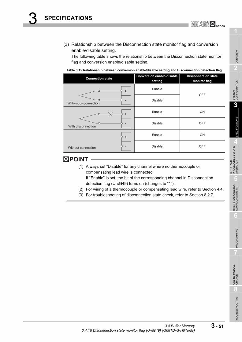
3 SPECIFICATIONS
1
OV
ER
VIE
W
2
SY
ST
EM
C
ON
FIG
UR
AT
ION
3
SP
EC
IFIC
AT
ION
S
4
SE
TU
P A
ND
P
RO
CE
DU
RE
S B
EF
OR
E
OP
ER
AT
ION
5
UT
ILIT
Y P
AC
KA
GE
(G
X
CO
NF
IGU
RA
TO
R-T
I)
6
PR
OG
RA
MM
ING
7
ON
LIN
E M
OD
ULE
C
HA
NG
E
8
TR
OU
BL
ES
HO
OT
ING
(3) Relationship between the Disconnection state monitor flag and conversion enable/disable setting.The following table shows the relationship between the Disconnection state monitor
flag and conversion enable/disable setting.
POINT(1) Always set “Disable” for any channel where no thermocouple or
compensating lead wire is connected.
If “Enable” is set, the bit of the corresponding channel in Disconnection
detection flag (Un\G49) turns on (changes to “1”).
(2) For wiring of a thermocouple or compensating lead wire, refer to Section 4.4.
(3) For troubleshooting of disconnection state check, refer to Section 8.2.7.
Table 3.15 Relationship between conversion enable/disable setting and Disconnection detection flag
Connection stateConversion enable/disable
setting
Disconnection state
monitor flag
Enable
OFF
Disable
Enable ON
Disable OFF
Enable ON
Disable OFF
Without disconnection
+
-
With disconnection
+
-
Without connection
+
-
3.4 Buffer Memory3.4.16 Disconnection state monitor flag (Un\G49) (Q68TD-G-H01only)
3 - 51

3 SPECIFICATIONS
3.4.17 CH[ ] Scaling value (Un\G50 to Un\G57)
The result of scaling measured temperature values is stored.
(1) Data storage
Measured temperature values within the scaling range set in CH Scaling range
upper/lower limit values (Un\G62 to Un\G77) are scaled to the scaling width set in
CH Scaling width upper/lower limit values (Un\G78 to Un\G93), and then the result
is stored.
(2) How to calculate the scaling value.The following is how to calculate the scaling value.
Figure 3.34 How to caluculate the scaling value
[Setting example] To scale a temperature to percent (for the use of thermocouple K)
(a) Setting value
• Scaling range: -100 to 500 (lower limit value = -1000, upper limit value = 5000)
• Scaling width: 0 to 100% (lower limit value = 0, upper limit value = 100)
(b) Input value
CH1 measured temperature value: 360 (Measured temperature value = 3600)
Figure 3.35 Setting example of scaling value
POINT(1) If the upper limit value is less than the lower limit value in the settings of CH
Scaling range upper/lower limit values (Un\G62 to Un\G77) or CH Scaling
width upper/lower limit values (Un\G78 to Un\G93), it will not result in an error
and the scaling value calculated with the expression above will be output.
(2) When the measured temperature is out of the range set in Scaling range
uppr/lower limit values, the value set in Scaling width upper limit value or
lower limit value is stored into this buffer memory.
Scaling value =
+ scaling width lower limit valuemeasured temperature value - scaling range lower limit value
scaling range upper limit value - scaling range lower limit value
(scaling width upper limit value - scaling width lower limit value)
Scaling value =
Fractional portion is rounded off.
Stores into buffer memory address 50.
(100 - 0) 76.666666
= 77[%]
+ 0 =3600 - (-1000)
5000 - (-1000)
3 - 52 3.4 Buffer Memory3.4.17 CH[ ] Scaling value (Un\G50 to Un\G57)

3 SPECIFICATIONS
1
OV
ER
VIE
W
2
SY
ST
EM
C
ON
FIG
UR
AT
ION
3
SP
EC
IFIC
AT
ION
S
4
SE
TU
P A
ND
P
RO
CE
DU
RE
S B
EF
OR
E
OP
ER
AT
ION
5
UT
ILIT
Y P
AC
KA
GE
(G
X
CO
NF
IGU
RA
TO
R-T
I)
6
PR
OG
RA
MM
ING
7
ON
LIN
E M
OD
ULE
C
HA
NG
E
8
TR
OU
BL
ES
HO
OT
ING
3.4.18 Scaling valid/invalid setting (Un\G58)
This area is for checking the scaling function valid/invalid status for each channel.
(1) Setting methods
(a) Scaling valid/invalid setting is set for each channel.
Figure 3.36 Setting of Scaling valid/invalid setting (Un\G58)
(b) Turn on Operating condition setting request (Y9) to activate the setting.
(2) Default valueAll channels are set to “Invalid” (00FFH).
[Program example]
Program example with a condition of the following is below.
• Scaling range: -100 to 500 (lower limit value = -1000, upper limit value = 5000)
• Scaling width: 0 to 100.0% (lower limit value = 0, upper limit value = 100)
Figure 3.37 Program example of scaling function
b15 b14 b13 b12 b11 b10 b9 b8 b7 b6 b5 b4 b3 b2 b1 b0
CH8 CH7 CH6 CH5 CH4 CH3 CH2 CH10 0 0 0 0 0 0 0
Data for b8 to b15 is fixed to "0".0: Valid
1: Invalid
Sets CH1 scaling function to
"enable"
Sets CH1 scaling range lower
limit value
Sets CH1 scaling range upper
limit value
Sets CH1 scaling width lower
limit value
Sets CH1 scaling width upper
limit value
Turns ON operating condition
seting request (Y9)
Turns OFF operating condition
setting request (Y9)
3.4 Buffer Memory3.4.18 Scaling valid/invalid setting (Un\G58)
3 - 53

3 SPECIFICATIONS
3.4.19 CH[ ] Scaling range upper/lower limit values (Un\G62 to Un\G77)
A scaling range of measured temperature values is set for each channel in units of 0.1 .
(1) Setting methods
(a) For use of the scaling function, change the setting value.
(b) Set the scaling range value in buffer memory.
• Settable scaling range: -32768 to 32767
(c) Turn on Operating condition setting request (Y9) to activate the setting.
(2) Default valueAll channels are set to "0".
POINT(1) When the measured temperature is out of the range set in Scaling range
uppr/lower limit values, the value set in Scaling width upper limit value or
lower limit value is stored into CH Scaling value (Un\G50 to Un\G57).
(2) Set “Valid” (“1”) in Scaling valid/invalid setting (Un\G58). When “Invalid” (“0”)
is set in the setting of the Scaling valid/invalid setting (Un\G58), CH Scaling
range upper/lower limit values (Un\G62 to Un\G77) is ignored.
(3) If the same value is set for the upper limit and the lower limit, an error (error
code: 91 ) occurs on the corresponding channel. Then, the following occurs.
• Error code (91 ) is stored into Error code (Un\G19). (Refer to Section
8.1).
• Error flag (XF) turns on.
• The module operates with setting before the error occurence.
3 - 54 3.4 Buffer Memory3.4.19 CH[ ] Scaling range upper/lower limit values (Un\G62 to Un\G77)

3 SPECIFICATIONS
1
OV
ER
VIE
W
2
SY
ST
EM
C
ON
FIG
UR
AT
ION
3
SP
EC
IFIC
AT
ION
S
4
SE
TU
P A
ND
P
RO
CE
DU
RE
S B
EF
OR
E
OP
ER
AT
ION
5
UT
ILIT
Y P
AC
KA
GE
(G
X
CO
NF
IGU
RA
TO
R-T
I)
6
PR
OG
RA
MM
ING
7
ON
LIN
E M
OD
ULE
C
HA
NG
E
8
TR
OU
BL
ES
HO
OT
ING
3.4.20 CH[ ] Scaling width upper/lower limit values (Un\G78 to Un\G93)
A width for scaling conversion is set.
(1) Setting methods
(a) For use of the scaling function, change the setting value.
(b) Set the scaling range value in buffer memory.
• Settable scaling range: -32768 to 32767
(c) Turn on Operating condition setting request (Y9) to activate the setting.
(2) Default valueAll channels are set to "0".
POINT(1) When “Invalid” (“0”) is set in Scaling valid/invalid setting (Un\G58), the setting
of CH Scaling width upper/lower limit values (Un\G78 to Un\G93) is ignored.
(2) If the same value is set for the upper limit and the lower limit, an error (error
code: 91 ) occurs on the corresponding channel. Then, the following occurs.
• Error code (91 ) is stored into Error code (Un\G19). (Refer to Section
8.1).
• Error flag (XF) turns on.
• The module operates with setting before the error occurence.
3.4 Buffer Memory3.4.20 CH[ ] Scaling width upper/lower limit values (Un\G78 to Un\G93)
3 - 55

3 SPECIFICATIONS
3.4.21 CH[ ] Process alarm upper/lower limit values (Un\G94 to Un\G125)
Process alarm upper upper limit value, upper lower limit value, lower upper limit value, and
lower lower limit value can be set. (Refer to Section 3.2.4)
(1) Setting methods
(a) A scaling range of measured temperature values is set for each channel in units of
0.1 .
Settable range and default value differ according to the thermocouple type.
The following table shows settable range and default value for each thermocouple
type.
(b) Turn on Operating condition setting request (Y9) to activate the setting.
POINT(1) If any of the following values are set, an error (error code: 6 ) occurs.
Then, Error flag (XF) turns on.
• A value out of the above settable range:
• A value that does not satisfy the following condition:
Process alarm lower lower limit value lower upper limit value upper lower limit value
upper upper limit value
(2) When “Disable” (“0”) is set in the Warning output enable/disable setting
(Un\G46), the setting of CH Process alarm upper/lower limit values
(Un\G94 to Un\G125) is ignored.
Table 3.16 Process alarm settable range and default value
Thermocouple
type
Default value
Settable temperature range (Accuracy
gurantee range)
Process
alarm
lower
lower
limit
value
Process
alarm
lower
upper
limit
value
Process
alarm
upper
lower
limit
value
Process
alarm
upper
upper
limit
value
Thermocouple K -2000 12000 -2700 to 13700 (-2000 to 12000)
Thermocouple E -2000 9000 -2700 to10000 (-2000 to 9000)
Thermocouple J -400 7500 -2100 to12000 (-400 to 7500)
Thermocouple T -2000 3500 -2700 to 4000 (-2000 to 3500)
Thermocouple B 6000 17000 0 to18200 (6000 to17000)
Thermocouple R 0 16000 -500 to17600 (0 to16000)
Thermocouple S 0 16000 -500 to17600 (0 to16000)
Thermocouple N -2000 12500 -2700 to13000 (-2000 to12500)
3 - 56 3.4 Buffer Memory3.4.21 CH[ ] Process alarm upper/lower limit values (Un\G94 to Un\G125)

3 SPECIFICATIONS
1
OV
ER
VIE
W
2
SY
ST
EM
C
ON
FIG
UR
AT
ION
3
SP
EC
IFIC
AT
ION
S
4
SE
TU
P A
ND
P
RO
CE
DU
RE
S B
EF
OR
E
OP
ER
AT
ION
5
UT
ILIT
Y P
AC
KA
GE
(G
X
CO
NF
IGU
RA
TO
R-T
I)
6
PR
OG
RA
MM
ING
7
ON
LIN
E M
OD
ULE
C
HA
NG
E
8
TR
OU
BL
ES
HO
OT
ING
3.4.22 CH[ ] Rate alarm warning detection period (Un\G126 to Un\G133)
The number of conversion periods to check a change in measured temperature values is
set for each channel. (Refer to Section 3.2.4)
(1) Setting methods
(a) For use of the rate alarm, change the setting value.
(b) Set the number of conversion periods in buffer memory.
• Settable range: 1 to 6000(times)
(c) Turn on Operating condition setting request (Y9) to activate the setting.
(2) Default valueAll channels are set to “0”.
POINT(1) When a value out of the above setting range is set, an error (error code: 70 )
occurs on the corresponding channel. Then, the following occurs.
• Error code (71 ) is stored into the Error code (Un\G19). (Refer to Section
8.1).
• Error flag (XF) turns on.
• The module operates with setting before the error occurence.
(2) Set “Enable” in Warning output enable/disable (Un\G46). When “Disable” is
set, the settings of CH Rate alarm warning detection period (Un\G126 to
Un\G133) is ignored.
3.4.23 CH[ ] Rate alarm upper/lower limit values (Un\G134 to Un\G149)
A scaling range of measured temperature values is set for each channel in units of
0.1 .(Refer to Section 3.2.4)
(1) Setting methods
(a) For use of the rate alarm, change the setting value.
(b) Set the range in buffer memory.
• Settable range:-32768 to 32767
(c) Turn on Operating condition setting request (Y9) to activate the setting.
(2) Default valueAll channels are set to "0".
3.4 Buffer Memory3.4.22 CH[ ] Rate alarm warning detection period (Un\G126 to Un\G133)
3 - 57

3 SPECIFICATIONS
3.4.24 Mode switching setting (Un\G158, Un\G159)
This area is used to switch the mode between normal mode and offset/gain setting mode.
This mode can be switched without resetting the programmable controller CPU.
Setting methods
(a) Set the setting value of the switching target mode.
(b) To switch the mode, turning on Operating condition setting request (Y9) after
setting the value is required.
(c) When the mode is switched completely, this area for Un\G158 and Un\G159 is
cleared to “0”.
POINTIf a value other than the setting values in Table 3.17 is written, mode switching is
not performed.
Table 3.17 Switching target mode and setting value
Switching target modeSetting value
Un\G158 Un\G159
Normal mode 0964H 4144H
Offset/gain setting value mode 4144H 0964H
3 - 58 3.4 Buffer Memory3.4.24 Mode switching setting (Un\G158, Un\G159)

3 SPECIFICATIONS
1
OV
ER
VIE
W
2
SY
ST
EM
C
ON
FIG
UR
AT
ION
3
SP
EC
IFIC
AT
ION
S
4
SE
TU
P A
ND
P
RO
CE
DU
RE
S B
EF
OR
E
OP
ER
AT
ION
5
UT
ILIT
Y P
AC
KA
GE
(G
X
CO
NF
IGU
RA
TO
R-T
I)
6
PR
OG
RA
MM
ING
7
ON
LIN
E M
OD
ULE
C
HA
NG
E
8
TR
OU
BL
ES
HO
OT
ING
3.4.25 Conversion setting for disconnection detection (Un\G164, Un\G165) (Q68TD-G-H02 only)
When disconnection is detected, a value stored into CH Measured temperature value
(Un\G11toUn\G18) is set. (Refer to Section 3.2.2)
The value to be stored is selected from “Up scale”, “Down scale” or “Given value”.
(1) Setting methods
(a) Set the value to be stored into buffer memory.
Figure 3.38 Setting of Conversion setting for disconnection detection (Un\G164, Un\G165)
The value to be stored into CH Measured temperature value (Un\G11toUn\G18)
changes as follows, depending on the setting value.
1) Up scale (0H)
Up-scale of the range currently set is stored.
2) Down scale (1H)
Down-scale of the range currently set is stored.
3) Given value (2H)
The value set in CH Conversion setting value for disconnection detection
(Un\G166toUn\G173) is stored.
(b) Turn on Operating condition setting request (Y9) to activate the setting.
(2) Default valueAll channels are set to “Down scale” (1111H).
POINTIf a value out of the setting range is set, the module operates with the default
setting, “Down scale”(1H).
b15 b12 b11 b8 b7 b4 b3 b0
CH8 CH7 CH6 CH5
CH4 CH3 CH2 CH1Un\G164 (Conversion setting for
disconnection detection CH1-4)
Un\G165 (Conversion setting for
disconnection detection CH5-8)
Measured temperature value at the
time of disconnection detection
Up scale
Down scale
Given value
Setting
value
to to to to
0H
1H
2H
3.4 Buffer Memory3.4.25 Conversion setting for disconnection detection (Un\G164, Un\G165) (Q68TD-G-H02 only)
3 - 59

3 SPECIFICATIONS
3.4.26 Disconnection state conversion setting (Un\G164, Un\G165) (Q68TD-G-H01only)
When disconnection state is checked, a value stored into CH Measured temperature
value (Un\G11toUn\G18) is set. (Refer to Section 3.2.3)
The value to be stored is selected from “Up scale”, “Down scale” or “Given value”.
(1) Setting methods
(a) Set the value to be stored in buffer memory.
Figure 3.39 Setting of Disconnection state conversion setting (Un\G164, Un\G165)
The value to be stored into CH Measured temperature value (Un\G11toUn\G18)
in the disconnection state check changes as follows, depending on the setting
value.
1) Up scale (0H)
Up-scale of the range currently set is stored.
2) Down scale (1H)
Down-scale of the range currently set is stored.
3) Given value (2H)
The value set in CH Conversion setting for disconnection state value
(Un\G166toUn\G173) is stored.
(b) Turn on Operating condition setting request (Y9) to activate the setting.
(2) Default valueAll channels are set to “Down scale” (1111H).
POINTIf a value out of the setting range is set, the module operates with the default
setting, “Down scale”(1H).
0H
1H
2H
b15 b12 b11 b8 b7 b4 b3 b0
CH8 CH7 CH6 CH5
CH4 CH3 CH2 CH1Un\G164 (Disconnection state
conversion setting CH1 to CH4)
Un\G165 (Disconnection state
conversion setting CH5 to CH8)
Measured temperature value when
confirming disconnection state
Up scale
Down scale
Given value
Setting
value
to to to to
3 - 60 3.4 Buffer Memory3.4.26 Disconnection state conversion setting (Un\G164, Un\G165) (Q68TD-G-H01only)

3 SPECIFICATIONS
1
OV
ER
VIE
W
2
SY
ST
EM
C
ON
FIG
UR
AT
ION
3
SP
EC
IFIC
AT
ION
S
4
SE
TU
P A
ND
P
RO
CE
DU
RE
S B
EF
OR
E
OP
ER
AT
ION
5
UT
ILIT
Y P
AC
KA
GE
(G
X
CO
NF
IGU
RA
TO
R-T
I)
6
PR
OG
RA
MM
ING
7
ON
LIN
E M
OD
ULE
C
HA
NG
E
8
TR
OU
BL
ES
HO
OT
ING
3.4.27 CH[ ] Conversion setting value for disconnection detection (Un\G166 to Un\G173) (Q68TD-G-H02 only)
When “Give value” (2H) is set in Conversion setting for disconnection detection
(Un\G164,Un\G165), the value to be stored into CH Measured temperature value
(Un\G11toUn\G18) can be set by user. (Refer to Section 3.2.2)
(1) Setting methods
(a) Set the value to be stored in buffer memory in units of 0.1 .
• Settable range:-32768 to 32767
(b) Turn on Operating condition setting request (Y9) to activate the setting.
(2) Default valueAll channels are set to “0”.
[Setting example] When the value of 800 is stored into CH1 Measured temperature
value for disconnection detection.
1) Set the following in buffer memory.
• Conversion setting for disconnection detection (Un\G164):2H
• CH1 Conversion setting value for disconnection detection(Un\G166):8000
2) Turn on Operating condition setting request (Y9).
3.4.28 CH[ ] Conversion setting value for disconnection state (Un\G166 to Un\G173) (Q68TD-G-H01only)
When “Give value” (2H) is set in the Disconnection state conversion setting
(Un\G164,Un\G165), the value to be stored into CH Measured temperature value
(Un\G11toUn\G18) can be set by user in the disconnection state check. (Refer to Section
3.2.3)
(1) Setting methods
(a) Set the valuetobe stored in buffer memory in units of 0.1 .
• Settable range:-32768 to 32767
(b) Turn on Operating condition setting request (Y9) to activate the setting.
(2) Default valueAll channels are set to“0”.
[Setting example] When the value of 800 is stored into CH1 Measured temperature
value for the check of disconnection state
1) Set the following in buffer memory.
• Disconnection state conversion setting (Un\G164):2H
• CH1 Conversion setting value for disconnection state (Un\G166):8000
2) Turn on Operating condition setting request (Y9) to activate the setting.
3.4 Buffer Memory3.4.27 CH[ ] Conversion setting value for disconnection detection (Un\G166 to Un\G173) (Q68TD-G-H02
3 - 61

3 SPECIFICATIONS
3.4.29 Factory default offset/gain values, User range settings offset/gain values (Un\G190 to Un\G253)
This area is used to reset the offset/gain easily at online module change. (Refer to
CHAPTER 7)
(1) Purpose of this buffer memory
(a) When the offset/gain setting values of the user range setting are restored, the
data to be used are stored.
The data are stored (saved) in the following cases.
• When writing default setting by the utility
• When setting the operating condition (Y9 turns from off to on*1)
• When writing the offset/gain values in the offset/gain setting mode (YA turns
from off to on) * 1 The data are not saved when a setting value has been written in the Mode switching setting
(Un\G158,Un\G159).
(b) To restore the offset/gain values of the user range setting, set the data saved in
this area to the corresponding area of the restoring target module.
(2) How to save data during online module changeSave buffer memory data during online module change in the following procedure.
1) Turn on Operating condition setting request (Y9).
2) Compare the values of the Factory default offset/gain values, the User range
settings offset/gain values, and the User range settings resistance offset/gain
values (Un\G190 to Un\G253) to the values in the range reference table.
(Refer to Section 7.4)
3) When the values are appropriate, take down the buffer memory data
compared.
POINTThis area is not used for offset/gain setting.
For offset/gain setting, refer to Section 4.6.
3 - 62 3.4 Buffer Memory3.4.29 Factory default offset/gain values, User range settings offset/gain values (Un\G190 to Un\G253)
4 SETUP AND PROCEDURES BEFORE OPERATION
1
OV
ER
VIE
W
2
SY
ST
EM
C
ON
FIG
UR
AT
ION
3
SP
EC
IFIC
AT
ION
S
4
SE
TU
P A
ND
P
RO
CE
DU
RE
S B
EF
OR
E
OP
ER
AT
ION
5
UT
ILIT
Y P
AC
KA
GE
(G
X
CO
NF
IGU
RA
TO
R-T
I)
6
PR
OG
RA
MM
ING
7
ON
LIN
E M
OD
ULE
C
HA
NG
E
8
TR
OU
BL
ES
HO
OT
ING
CHAPTER 4 SETUP AND PROCEDURES BEFORE OPERATION
4.1 Handling Precautions
(1) Do not drop or give a strong impact to the case.
(2) Do not remove the printed-circuit board of the module from the case. Doing so may cause a failure.
(3) Be careful to prevent foreign matters such as cutting chips or wire chips from entering the module. Such foreign matter can cause a fire, failure, or malfunction.
(4) A protective film is attached to the module top to prevent foreign matter such as wire chips from entering the module during wiring.Do not remove the film during wiring. Be sure to remove it for heat dissipation before system operation.
(5) Tighten the screws such as module fixing screws within the following ranges.Undertigtening can cause drop of the screw, short circuit or malfunction.
* 1 The module can be easily fixed onto the base unit using the hook at the top of the module. When using the Q68TD-G-H02(H01) in an environment of frequent vibrations, fix the module with a module fixing screw.
(6) To mount the module, while pressing the module mounting lever located in the lower part of the module, fully insert the module fixing projection into the hole in the base unit and press the module until it snaps into place. Incorrect module mounting may cause a malfunction, failure, or drop of the module.After mounting the module to the base unit, fix the module with a module fixing bracket. (Q68TD-G-H02 only) (Refer to Section 4.1.1)When using the Q68TD-G-H01 in an environment of frequent vibrations, fix the module with a module fixing screw. (Q68TD-G-H01 only)
(7) Always make sure to touch the grounded metal to discharge the electricity charged in the body, etc., before touching the module. Failure to do so may cause a failure or malfunctions of the module.
Table 4.1 Tightening torque
Screw location Tightening torque range
Module fixing screw (M3 screw)*1 0.36 to 0.48N•m
Connector screw (M2.6 screw) 0.20 to 0.29N•m
4.1 Handling Precautions
4 - 1

4 SETUP AND PROCEDURES BEFORE OPERATION
4.1.1 Fixing module with module fixing bracket (Q68TD-G-H02 only)
After mounting the Q68TD-G-H02 to the base unit, fix the Q68TD-G-H02 module with a module fixing bracket.
POINTMake sure that the module fixing bracket is hooked on the third slit viewed from
the front of the Q68TD-G-H02. Then, tighten the module fixing screw within the
specified torque range.
Figure 4.1 Fixing module with module fixing bracket
Module fixing bracket
Module fixing screwQ68TD-G-H02
3rd slit
4 - 2 4.1 Handling Precautions4.1.1 Fixing module with module fixing bracket (Q68TD-G-H02 only)

4 SETUP AND PROCEDURES BEFORE OPERATION
1
OV
ER
VIE
W
2
SY
ST
EM
C
ON
FIG
UR
AT
ION
3
SP
EC
IFIC
AT
ION
S
4
SE
TU
P A
ND
P
RO
CE
DU
RE
S B
EF
OR
E
OP
ER
AT
ION
5
UT
ILIT
Y P
AC
KA
GE
(G
X
CO
NF
IGU
RA
TO
R-T
I)
6
PR
OG
RA
MM
ING
7
ON
LIN
E M
OD
ULE
C
HA
NG
E
8
TR
OU
BL
ES
HO
OT
ING
4.2 Setup and Procedures before Operation
Figure 4.2 Procedures and setting before system operation
Initial setting and automatic refresh setting
The program can be simplified if the utility
package is used for setting.
Programming and debugging
Create and check the sequence program.
NO
YES
Use the utility package?
Offset/gain setting
If user range settings are used, perform the
offset and gain settings.
Use factory default settings
Use user range settings?
Use user range settings
Intelligent function module switch settings
Perform settings using GX Developer.
Module mounting
Mount the Q68TD-G-H02(H01) in the specified slot.
Start
Wiring
Wire the thermocouple and cold junction temperature
compensation resistor to the Q68TD-G-H02(H01).
If the terminal block is used, connect the thermocouple
and cold junction temperature compensation resistor
to it. Then wire the terminal block to the
Q68TD-G-H02(H01).
(Refer to CHAPTER 5).
4.2 Setup and Procedures before Operation
4 - 3

4 SETUP AND PROCEDURES BEFORE OPERATION
4.3 Part Names
The following explains the part names of the Q68TD-G-H02(H01).
The part names and signal names of the Q68TD-G-H02 and Q68TD-G-H01 are same.
(1) Q68TD-G-H02
(2) Q68TD-G-H01
(Connector
terminal
number)
(Connector
terminal
number)
A1
A20
B1
B20
3)1)
2)
Module fixing screw Module fixing bracket
4)
(Connectorterminalnumber)
(Connectorterminalnumber)
A1
A20
B1
B20
3)1)
2)
4)
4 - 4 4.3 Part Names

4 SETUP AND PROCEDURES BEFORE OPERATION
1
OV
ER
VIE
W
2
SY
ST
EM
C
ON
FIG
UR
AT
ION
3
SP
EC
IFIC
AT
ION
S
4
SE
TU
P A
ND
P
RO
CE
DU
RE
S B
EF
OR
E
OP
ER
AT
ION
5
UT
ILIT
Y P
AC
KA
GE
(G
X
CO
NF
IGU
RA
TO
R-T
I)
6
PR
OG
RA
MM
ING
7
ON
LIN
E M
OD
ULE
C
HA
NG
E
8
TR
OU
BL
ES
HO
OT
ING
* 1 When the module is mounted on a MELSECNET/H remote I/O station, the RUN LED stays off until a data link starts normally, even after the power is turned on. The RUN LED turns on once a data link starts.
* 1 For actual wiring, refer to Section 4.4.2 External Wiring.
(3) Connector for external wiringThe connectors for use with the Q68TD-G-H02 (H01) should be purchased separately
by the user.
The following tables show the connector types and the crimp-contact tool.
Table 4.2 Part names
Number Name Description
1) RUN LED
Displays the operating status of the Q68TD-G-H02(H01).
On : Normal operation
Flashing : During offset/gain setting mode
Off : 5V power supply interrupted, watchdog timer error occurred, or online module
change enabled.
2) ERR. LED
Displays the error status of the Q68TD-G-H02(H01).
On : Error
Flashing : Error in switch settings
Switch No. 5 of the intelligent function module has been set to a value other
than zero.
Off : Normal operation
3) ALM LED
Displays the warning status of the Q68TD-G-H02(H01).
On : Warning (process alarm, rate alarm) occurring (Refer to Section 3.4.13)
Flashing :Disconnection detected (Q68TD-G-H02)
Checking a disconnection status (Q68TD-G-H01)
Off : Normal operation
4) Serial No. display Displays the serial No. of the Q68TD-G-H02 (H01).
Table 4.3 Signal name
Terminal
numberSignal name
Terminal
numberSignal name
A1 CH1+ B1 CH1-
A2 --- B2 ---
A3 CH2+ B3 CH2-
A4 --- B4 ---
A5 CH3+ B5 CH3-
A6 --- B6 ---
A7 CH4+ B7 CH4-
A8 --- B8 ---
A9 CH5+ B9 CH5-
A10 --- B10 ---
A11 CH6+ B11 CH6-
A12 --- B12 ---
A13 CH7+ B13 CH7-
A14 --- B14 ---
A15 CH8+ B15 CH8-
A16 --- B16 ---
A17 --- B17 ---
A18 --- B18 ---
A19 --- B19 RTD+
A20 RTDG B20 RTD-
B20
B19
B18
B17
B16
B15
B14
B13
B12
B11
B10
B9
B8
B7
B6
B5
B4
B3
B2
B1
A20
A19
A18
A17
A16
A15
A14
A13
A12
A11
A10
A9
A8
A7
A6
A5
A4
A3
A2
A1
Seen from the front
of the module
Figure 4.3 Terminal number
4.3 Part Names
4 - 5

4 SETUP AND PROCEDURES BEFORE OPERATION
(a) Connector types*1
* 1 The A6CON3 (pressure-displacement type, straight out) connector cannot be used for the Q68TD-G-H02 (H01).
(b) Crimp-contact tool
Type Model name Applicable wire size
Soldering type
(straight out)A6CON1 0.3mm2 (AWG22) (stranded)
Crimp-contact type
(straight out)A6CON2 0.088mm2 to 0.24mm2 (AWG28 to 24) (stranded)
Soldering type
(straight out/diagonal out)A6CON4 0.3mm2(AWG22) (stranded)
Type Model name Applicable wire size Contact
Crimp-contact tool FCN-363T-T005/H 0.088mm2 to 0.24mm2(AWG28 to 24)FUJITSU COMPONENT LIMITED
www.fcl.fujitsu.com/en
4 - 6 4.3 Part Names

4 SETUP AND PROCEDURES BEFORE OPERATION
1
OV
ER
VIE
W
2
SY
ST
EM
C
ON
FIG
UR
AT
ION
3
SP
EC
IFIC
AT
ION
S
4
SE
TU
P A
ND
P
RO
CE
DU
RE
S B
EF
OR
E
OP
ER
AT
ION
5
UT
ILIT
Y P
AC
KA
GE
(G
X
CO
NF
IGU
RA
TO
R-T
I)
6
PR
OG
RA
MM
ING
7
ON
LIN
E M
OD
ULE
C
HA
NG
E
8
TR
OU
BL
ES
HO
OT
ING
4.4 Wiring
The following explains the wiring precautions and module connection example.
4.4.1 Wiring precautions
External wiring that is less susceptible to noise is required as a condition of enabling a
highly reliable system and making full use of the capabilities of the Q68TD-G-H02(H01).
(1) Use separate cables for the AC control circuit and the external input signals of the Q68TD-G-H02(H01) to avoid the influence of the AC side surges and inductions.
(2) Always place the thermocouple at least 100mm away from the main circuit cables and AC control circuit lines. Fully keep it away from high-voltage cables and circuits, which include high frequency waves, such as an inverter's load circuit. Not doing so will cause the module more susceptible to noises, surges and inductions.
(3) The following wiring is required for the product to comply with the EMC and Low Voltage Directives.
Figure 4.4 Wiring complying with EMC and LOW Voltage Directives
(a) Use shielded cables for every external wiring and use the AD75CK cable clamp to
ground to the panel. AD75CK can ground four cables together when using cables
with outer diameter of about 7mm.
(b) Use shielded cabled between the external device connector and the relay terminal
block, and ground it to the control panel. The cable must be 3m or shorter.
(c) Before touching the relay terminal block, always touch the grounded metal to
discharge the electricity charged in the body.
In a control panel
20 to 30cm
Q68TD-G-H02(H01)
Relay terminalblock
External device connector
Strip off the outer sheath
AD75CK
4.4 Wiring4.4.1 Wiring precautions
4 - 7

4 SETUP AND PROCEDURES BEFORE OPERATION
4.4.2 External wiring
(1) Wiring procedure
1) Install a relay terminal block for wiring.
2) Connect the thermocouple and the compensation conductors to the relay
terminal block.
3) When setting the Q68TD-G-H02(H01) to "With cold junction temperature
compensation", connect the cold junction temperature compensation resistor
(RTD), which is supplied with Q68TD-G-H02(H01), to the relay terminal block.
4) Wire Q68TD-G-H02 (H01) to the relay terminal block using an external device
connector.
+
-
+
-
+
G
-
+
-
CH1
+
-
CH8
+
G
-
RTD
A1
B1
A15
B15
A20
B19
B20
Q68TD-G-H02(H01)
Cable(*1)
RTD
CH1
CH8
RTD
Compensation
conductors
(*2)
(*4)
(*3)
Relay
terminal block External device connector
Mo
du
lato
r
De
mo
du
lato
r
Mo
du
lato
r
De
mo
du
lato
r
Filt
er
Input am
plif
er
*1 Use shielded cables, and ground the shields.
Do not use compensation conductors.
*2 Use shielded compensation conductors, and ground the shields.
Do not use cables.
*3 When setting the Q68TD-G-H02(H01) to "With cold junction temperature compensation",
always connect the cold junction temperature compensation resistor (RTD).
*4 When connecting the RTD, always connect the terminals between RTD- and RTD G.
4 - 8 4.4 Wiring4.4.2 External wiring

4 SETUP AND PROCEDURES BEFORE OPERATION
1
OV
ER
VIE
W
2
SY
ST
EM
C
ON
FIG
UR
AT
ION
3
SP
EC
IFIC
AT
ION
S
4
SE
TU
P A
ND
P
RO
CE
DU
RE
S B
EF
OR
E
OP
ER
AT
ION
5
UT
ILIT
Y P
AC
KA
GE
(G
X
CO
NF
IGU
RA
TO
R-T
I)
6
PR
OG
RA
MM
ING
7
ON
LIN
E M
OD
ULE
C
HA
NG
E
8
TR
OU
BL
ES
HO
OT
ING
POINTIn the following cases (1) and (2), the cold junction temperature compensation
resistor (RTD) and the end part of a thermocouple (or the end part of a
compensating lead wire) are not connected to the same part, the relay terminal
block. In such cases, the measured temperature value may be abnormal due to
ambient temperature difference.
(1) As the following figure, when the end part of the thermocouple and relay
terminal block are connected by a cable, the measured temperature may be
abnormal due to ambient temperature difference between A and B.
Figure 4.5 When the end part of the thermocouple and relay terminal block are connected by a cable
(2) As the following figure, when the relay terminal block and the Q68TD-G-H02
(H01) are connected by a compensating lead wire, the measured temperature
may be abnormal due to ambient temperature difference between B and C.
Figure 4.6 When the relay terminal block and the Q68TD-G-H02 (H01) are connected by a compensating lead wire
End part
A
B
RTD
(Correct) Compensating
lead wire
(Incorrect) Cable Cable
Ambient temperature difference
Relay
terminal block Q68TD-G-H02(H01)
A: End part of the thermocouple
B: Cold junction temperature
compensation resistor (RTD)
End part
CB
RTD
(Correct) Cable
(Incorrect)
Compensating
lead wireCompensating lead wire
Ambient temperature difference
Relay
terminal block Q68TD-G-H02(H01)
B: Cold junction temperature
compensation resistor (RTD)
C: End part of the compensating lead wire
4.4 Wiring4.4.2 External wiring
4 - 9

4 SETUP AND PROCEDURES BEFORE OPERATION
(2) When a connector/terminal block converter module is usedA connector/terminal block converter module for the Q68TD-G-H02 (H01) and
dedicated cables are available.
To use the connector/terminal block converter module, wire modules as shown below.
Figure 4.7 Example of the wiring using a connector/terminal block converter module
* 1 When setting the Q68TD-G-H02 (H01) to "With cold junction temperature compensation", always connect the cold junction temperature compensation resistor (RTD).
* 2 Always ground the shields. * 3 Since RTD- and RTD G are internally connected in the connector/terminal block converter
module, connection of RTD- and RTD G at the terminal block is not required.
For inquiries related to the products or your order, please consult your local Mitsubishi
Electric sales office or representative.
Table 4.4 List of the model names
Product name Model name Remarks Manufacturer
Connector/terminal
block converter
module
FA-LTB40TDG -
Mitsubishi Electric Engineering Co.,
Ltd.
Dedicated cable
FA-CBL05Q68TDG Cable length: 0.5m
FA-CBL10Q68TDG Cable length: 1.0m
FA-CBL20Q68TDG Cable length: 2.0m
FA-CBL30Q68TDG Cable length: 3.0m
Q68TD-G-H02(H01)
RTD
RTD+
RTD-
RTD G
Dedicated cable
Shield (*2)
Connector/terminal block converter module
Compensating lead wire
Shield (*2)
CH1+ (terminal 1)
CH1- (terminal 2)
RTD+ (terminal 38)
RTD- (terminal 40)
(*1)
Module internal wiring (*3)
4 - 10 4.4 Wiring4.4.2 External wiring

4 SETUP AND PROCEDURES BEFORE OPERATION
1
OV
ER
VIE
W
2
SY
ST
EM
C
ON
FIG
UR
AT
ION
3
SP
EC
IFIC
AT
ION
S
4
SE
TU
P A
ND
P
RO
CE
DU
RE
S B
EF
OR
E
OP
ER
AT
ION
5
UT
ILIT
Y P
AC
KA
GE
(G
X
CO
NF
IGU
RA
TO
R-T
I)
6
PR
OG
RA
MM
ING
7
ON
LIN
E M
OD
ULE
C
HA
NG
E
8
TR
OU
BL
ES
HO
OT
ING
4.5 Switch Setting for Intelligent Function Module
The settings for the intelligent function module are performed using the I/O assignment
settings for GX Developer.
(1) Setting itemIntelligent function module switch has switches 1 to 5.The setting is executed with 16-
bit data.
When not setting the intelligent function module switch, the default of switches 1 to 5
is 0.
* 1 Setting any value within the setting range will provide the same operation. When the setting range is 1H to FH, set 1H for example.
* 2 Setting a value other than "0H" results in an error.
Table 4.5 Intelligent Function Module Switch Settings
Setting Item
Switch 1
Thermocouple type
settings
(CH1 to CH4)
Thermocouple type Setting value
Thermocouple K 0H
Thermocouple E 1H
Thermocouple J 2H
Thermocouple T 3H
Switch 2
Thermocouple type
settings
(CH5 to CH8)
Thermocouple B 4H
Thermocouple R 5H
Thermocouple S 6H
Thermocouple N 7H
Setting a value other than 0H to 7H results in a range setting
error (error code: 10 ) and the measured temperature is
not converted. ( indicates the error corresponding channel
number.)
Switch 3
Offset/gain setting mode
Switch 4
Mode setting, Cold junction compensation setting
Switch 5 0H : Fixed *2
CH4 CH3 CH2 CH1
H
CH8 CH7 CH6 CH5
H
0: Factory default setting1: User range setting
H0 0
b7 b6 b5 b4 b3 b2 b1 b0
CH8 CH7 CH6 CH5 CH4 CH3 CH2 CH1
Fixed to 0H
: Normal mode : offset/gain setting mode
: With cold junction temperature compensation : Without cold junction temperature compensation
H
Fixed to 0H
0H
1H to FH*1
0H
1H to FH*1
00
4.5 Switch Setting for Intelligent Function Module
4 - 11

4 SETUP AND PROCEDURES BEFORE OPERATION
(2) Operating procedureStart the settings with GX Developer assignment setting screen.
(a) I/O assignment setting screen
Set the following for the slot in which the Q68TD-G-H02(H01) is mounted.
The type setting is required; set other items as needed.
Type : Select "intelli."
Model name : Enter the module model name.
Points : Select 16 points.
Start XY : Enter the start I/O number for the Q68TD-G-H02(H01).
Detail setting: Specify the control PLC for the Q68TD-G-H02(H01).
It is unnecessary to set the "Error time output mode" or "H/W error time PLC
operation mode" since these settings are invalid for the Q68TD-G-H02(H01).
Figure 4.8 I/O assignment tab
(b) Switch setting for intelligent function module screen
Click on [Switch setting] on the I/O assignment setting screen to display the
screen shown at left, then set switches 1 to 5.
The switches can easily be set if values are entered in hexadecimal. Change the
entry format to hexadecimal and then enter the values.
Figure 4.9 Switch setting for intelligent function module screen
4 - 12 4.5 Switch Setting for Intelligent Function Module

4 SETUP AND PROCEDURES BEFORE OPERATION
1
OV
ER
VIE
W
2
SY
ST
EM
C
ON
FIG
UR
AT
ION
3
SP
EC
IFIC
AT
ION
S
4
SE
TU
P A
ND
P
RO
CE
DU
RE
S B
EF
OR
E
OP
ER
AT
ION
5
UT
ILIT
Y P
AC
KA
GE
(G
X
CO
NF
IGU
RA
TO
R-T
I)
6
PR
OG
RA
MM
ING
7
ON
LIN
E M
OD
ULE
C
HA
NG
E
8
TR
OU
BL
ES
HO
OT
ING
4.6 Offset/Gain Setting
Execute offset/gain settings in the following procedure.
When the factory shipped setting is used, offset/gain setting is not necessary.
If the utility package is installed, execute the offset/gain setting according to the procedure
in Section 5.6.2.
(1) Setting procedure
Figure 4.10 Setting procedure for offset/gain setting
YES
NO
1)
1)
2)
Set the gain setting channel in the offset/gain setting
mode (Gain specification)(Un\G27). Set the offset/gain
setting mode (Offset specification)(Un\G26) to "0".
Check that "RUN" LED is flashing to indicate the
offset/gain setting mode.
Switch to the offset/gain setting mode. *2
Confirm that the channel change completion flag
(XB) is turned ON.
Enter the value, to be used as gain value in the termocouple or standard DC voltage generator, to channel for adjusting.
Confirm that the offset/gain setting mode status flag
(XA) is turned OFF.
Write the temperature setting value (digital) equivalent to the analog input value to the CH gain temperature setting value (Un\G29)*4 of the channel to be adjusted.
Set the offset setting channel in the offset/gain
setting mode (Offset specification)(Un\G26). Set the
offset/gain setting mode (Gain specification)
(Un\G27) to "0".
Set the conversion enable/disable setting (Un\G0)
of the channel for executing the offset/gain setting
to "enable" and turnY9 from ON to OFF. *3
With the intelligent function module swich setting,
set the input type setting value to a type for executing
error compensation. In the cold junction temperature
compensation setting, set it to "with cold junction
temperature compensation". *1
Confirm that the channel change completion flag
(XB) is turned ON.
Enter the value, to be used as a offset value in the termocouple or standard DC voltage generator, to channel for adjusting.
Turn OFF the channel change request (YB).
Turn ON the channel change request (YB).
Turn ON the channel change request (YB).
Turn OFF the channel change request (YB).
Turn ON the user range write request (YA).
Turn OFF the user range write request (YA).
Switch to normal mode.
START
Do you want to adjust other channels?
Is the disconnection
detection signal (XC)
(Q68TD-G-H02 only) or disconnection
state monitor signal (XC)
(Q68TD-G-H01 only)
ON?
YES
NO
YES
NO
2)Is the "ERR." LED on?
FINISH
Check the disconnection
detection flag (Un\G49)
(Q68TD-G-H02 only) or
disconnection state
monitor flag (Un\G49)
(Q68TD-G-H01 only),
and identify the channel
for the disconnection.
Then review the wiring
of the channel and turn
YF from ON to OFF.
Write the temperature setting value (digital) equivalent to the analog input value to the CH offset temperature setting value (Un\G28)*4 of the channel to be adjusted.
4.6 Offset/Gain Setting
4 - 13

4 SETUP AND PROCEDURES BEFORE OPERATION
* 1 When inputting a value using such as a standard DC voltage generator, or using without cold junction temperature compensation on actual use, set it to "without cold junction compensation".
* 2 The mode switching (normal mode to offset/gain setting mode to normal mode) method is indicated below.
* 3 For the conversion enable/disable setting of unused channels or channels not executing the offset/gain setting, always set it to "disable".If all channels are set to "Enable", Disconnection detection flag (Disconnection state monitor flag) (Un\G49) of channels that are not connecting a thermocouple turns on (changes to "1")
* 4 Buffer memory address of channel 1 only is indicated in the chart. For buffer memory address of other channels, refer to Section 3.4.1 Buffer memory assignment.
* 5 Do not perform the operations below during the steps indicated with *5. If they are performed, the data inside a flash memory will have a problem, and the Q68TD-G-H02 (H01) may not operate normally.
•Powering off the programmable controller CPU •Resetting the programmable controller CPU
Table 4.6 Mode switching method
Mode switching method Refer to
Dedicated instruction (G(P).OFFGAN)(2)(a) in this
section
Setting the mode switching setting (Un\G158, Un\G159) and turning from
OFF to ON the operating condition setting request (Y9).
(2)(b) in this
section
Intelligent function module switch setting
(After setting the intelligent function module switch, reset or turn from OFF
to ON the programmabel controller CPU.)
Section 4.5,
(2)(c) in this
section
4 - 14 4.6 Offset/Gain Setting

4 SETUP AND PROCEDURES BEFORE OPERATION
1
OV
ER
VIE
W
2
SY
ST
EM
C
ON
FIG
UR
AT
ION
3
SP
EC
IFIC
AT
ION
S
4
SE
TU
P A
ND
P
RO
CE
DU
RE
S B
EF
OR
E
OP
ER
AT
ION
5
UT
ILIT
Y P
AC
KA
GE
(G
X
CO
NF
IGU
RA
TO
R-T
I)
6
PR
OG
RA
MM
ING
7
ON
LIN
E M
OD
ULE
C
HA
NG
E
8
TR
OU
BL
ES
HO
OT
ING
POINT(1) Execute the offset/gain settings in the actual operating status.
(2) Offset value and gain value are stored in the Flash memory of the Q68TD-G-
H02(H01) by turning ON the user range write request (YA), and the values are
not erased at power-off. To prevent unnecessary write to Flash memory, an
error (error code 162) occures if writing is performed 26 times continuously.
(3) Execute the offset/gain setting within the measured temperature guarantee
range (refer to shaded area of Section 3.1 (2) Table 3.2).
If the setting exceeds the measrued temperature guarantee range, resolution
and accuracy may not be within the ranges of the performance specifications.
(4) Set the offset and gain values within the ranges where the following
conditions are satisfied.
(Gain value) - (offset value) > 0.1[ ]
Set the offset temperature setting value and gain temperature setting value
within the range where the following conditions are satisfied.
(Gain temperarure setting value) - (offset temperature setting value) > 0.1[ ]
(5) When the user range write request (YA) is turned ON, consistency check for
offset value and gain value, and offset temperature setting value and gain
temperature setting value is executed.
If an error occurs on any channel, offset/gain values are not written to the
module. Check the value of error code (Un\G19) and take an appropriate
measure. Then, execute offset/gaing setting again.
(6) Offset/gain setting can be exectued on multiple channels at the same time;
however, set the offset and gain separately.
Setting the offset and gain for channels at the same time results in an error,
and the [ERR.] LED turns on.
(7) It takes approximately seven seconds from when Channel change request
(YB) turns on till when Channel change completion flag (XB) turns on. During
this period, input to channels targeted for offset/gain setting must be constant.
In addition, if disconnection is detected or checked during this period,
Channel change completion flag (XB) turns on earlier and an error (error
code: 51 ) occurs simultaneously. If this occurs, perform offset/gain setting
again after connection is restored.
(8) If an error (error code: 51 ) described at (7) occurs while performing offset/
gain setting simultaneously on multiple channels, values are not set only for
the channel of which disconnection is detected or checked but also normally-
connected channels. Therefore, perform offset/gain setting again for all
adjusting target channels after connection is restored.
(9) The Module ready (X0) turns from OFF to ON when the offset/gain setting
mode is switched to the normal mode by the setting of the dedicated
instruction (G(P).OFFGAN) or mode switch settings (Un\G158, Un\G159).
Note that initial setting processing will be executed if there is a sequence
program that will execute initial setting when the Module ready (X0) turns ON.
(10)Warm-up (power distribution) period of 30 minutes is required to satisfy with
accuracy before the offset/gain setting is performed.
4.6 Offset/Gain Setting
4 - 15

4 SETUP AND PROCEDURES BEFORE OPERATION
(2) Program examples(a) The program in dotted area of (a) is common to (a),(b) and (c).
In this example, the I/O numbers for the Q68TD-G-H02(H01) are X/Y0 to X/YF.
Table 4.7 List of devices
Device Function
M0 Mode switching
M1 Channel selection
M2 Channel conversion enabling
M3 Offset setting
M4 Gain setting
M5 Channel change instruction
M6 Offset/gain setting value write command to module
M50 Switching to the offset/gain setting mode
M51 Switching to the normal mode
D0 Dedicated instruction (G(P).OFFGAN) setting value storage device
D1Channel specification storage device
D2
D3 Offset temperature setting value storage device
D4 Gain temperature setting value storage device
4 - 16 4.6 Offset/Gain Setting

4 SETUP AND PROCEDURES BEFORE OPERATION
1
OV
ER
VIE
W
2
SY
ST
EM
C
ON
FIG
UR
AT
ION
3
SP
EC
IFIC
AT
ION
S
4
SE
TU
P A
ND
P
RO
CE
DU
RE
S B
EF
OR
E
OP
ER
AT
ION
5
UT
ILIT
Y P
AC
KA
GE
(G
X
CO
NF
IGU
RA
TO
R-T
I)
6
PR
OG
RA
MM
ING
7
ON
LIN
E M
OD
ULE
C
HA
NG
E
8
TR
OU
BL
ES
HO
OT
ING
(a) When switching the mode using dedicated instruction (G(P).OFFGAN)
The following program example is for switching to the offset/gain setting mode
with the dedicated instruction (G(P).OFFGAN) and changing the channel for the
offset/gain setting, then writing the offset/gain values to the Q68TD-G-H02(H01)
and then switching to the normal mode.
Figure 4.11 When switching the mode using dedicated instruction (G(P).OFFGAN) * 1 The program in the dotted area is a common program.
Stores offset/gain setting
target channel.
Copies data of D1 into D2.
Inverts bit for conversion
enable/disable setting.
Sets conversion
enable/disable.
Turns ON Operating
condition setting request (Y9).
Turns OFF Operating
condition setting request (Y9).
Stores offset temperature
setting value into D3.
Writes value to Offset
temperature setting value.
Specifies offset setting
channel.
Sets "0" for gain setting
channel.
Stores gain temperature
setting value into D4.
Writes value to Gain
temperature setting value.
Sets "0" for offset setting
channel.
Specifies gain setting
channel.
Turns ON Channel change
request (YB).
Turns OFF Channel change
request (YB).
Turns ON User range write
request (YA).
Turns OFF User range write
request (YA).
Dedicated instruction
(G.OFFGAN)*1
Processing in normal mode
4.6 Offset/Gain Setting
4 - 17

4 SETUP AND PROCEDURES BEFORE OPERATION
(b) When switching the mode using the the mode switching setting (Un\G158,
Un\G159) and the operating condition setting request (Y9)
Figure 4.12 When switching the mode using the setting in the Mode switching setting (Un\G158,Un\G159) and Operating condition setting request (Y9)
(c) When switching the mode by making intelligent function module switch setting
Only the common program is necessary.
Stores "H4144" in Un\G1
Stores "H0964" in Un\G1
Stores "H0964" in Un\G1
Stores "H4144" in Un\G1
Common program
Processing in normal mode
4 - 18 4.6 Offset/Gain Setting

4 SETUP AND PROCEDURES BEFORE OPERATION
1
OV
ER
VIE
W
2
SY
ST
EM
C
ON
FIG
UR
AT
ION
3
SP
EC
IFIC
AT
ION
S
4
SE
TU
P A
ND
P
RO
CE
DU
RE
S B
EF
OR
E
OP
ER
AT
ION
5
UT
ILIT
Y P
AC
KA
GE
(G
X
CO
NF
IGU
RA
TO
R-T
I)
6
PR
OG
RA
MM
ING
7
ON
LIN
E M
OD
ULE
C
HA
NG
E
8
TR
OU
BL
ES
HO
OT
ING
4.7 Cold Junction Temperature Compensation with/without Setting
The Q68TD-G-H02(H01) can execute the following two different cold junction temperature
compensations by setting the inteligent function module switch setting (switch 4) to
whether to carry out the cold junction temperature compensation using the cold junction
temperature compensation resistor (RTD) or not.
(1) Executing cold junction temperature compensation with the cold junction temperature compensation resistor (RTD) (set to "with cold junction temperature compensation")Cold junction temperature compensation is possible by connecting the supplied cold
junction temperature compensation resistor (RTD) and setting it to "with cold junction
temperature compensation".
Always connect the supplied cold junction temperature compensation resistor (RTD)
to the terminal block. (For connection, refer to Section 4.4.2.)
Figure 4.13 Connection between a cold junction compensation resistor (RTD) and a relay terminal block
(2) Executing cold junction temperatuer compensation externally (set to "without cold junction temperature compensation")Use this function to measure temperature in higher accuracy than the cold junction
temperature compensation accuracy ( 1 ) by the cold junction temperature
compensation resistor (RTD) that is included with the Q68TD-G-H02 (H01).
Connecting a cold junction temperature compensation resistor (RTD) to the terminal
block is unnecessary.
By providing a precision ice bath externally, the thermoelectromotive force generated
at the tip of the thermocouple can be led to this module without any change, improving
the cold junction temperature compensation accuracy.
Figure 4.14 Connection between an ice bath and a relay terminal block
ThermocoupleCompensation conductor
Object whose temperature
is to be measuredTerminal block
Q68TD-G-H02(H01)
RTD
Compensation conductor
Ice bath
Object whose temperature
is to be measured
ThermocoupleConductor
Terminal block
Q68TD-G-H02(H01)
4.7 Cold Junction Temperature Compensation with/without Setting
4 - 19

4 SETUP AND PROCEDURES BEFORE OPERATION
POINTThe ice bath is designed to connect the thermocouple/compensation conductor
and conductor in the pot whose internal temperature is controlled to be 0 .
Hence, the thermoelectromotive force at the contact portion of the thermocouple/
compensation conductor and conductor will be 0mV, preventing the generation of
extra thermoelectromotive force which can cause errors.
4 - 20 4.7 Cold Junction Temperature Compensation with/without Setting

5 UTILITY PACKAGE (GX Configurator-TI)
1
OV
ER
VIE
W
2
SY
ST
EM
C
ON
FIG
UR
AT
ION
3
SP
EC
IFIC
AT
ION
S
4
SE
TU
P A
ND
P
RO
CE
DU
RE
S B
EF
OR
E
OP
ER
AT
ION
5
UT
ILIT
Y P
AC
KA
GE
(G
X
CO
NF
IGU
RA
TO
R-T
I)
6
PR
OG
RA
MM
ING
7
ON
LIN
E M
OD
ULE
C
HA
NG
E
8
TR
OU
BL
ES
HO
OT
ING
CHAPTER 5 UTILITY PACKAGE (GX Configurator-TI)
5.1 Utility Package Functions
Table 5.1 shows a list of the utility package functions.
Table 5.1 Utility Package (GX Configurator-TI) Function List
Function DescriptionReference
section
Initial
setting
(1) Make initial setting for operating the Q68TD-G-H02(H01) channel-by-channel.
Set the values of the items which require initial setting.
Section 5.4
•Conversion enable/disable setting •Rate alarm lower limit value
•Averaging processing selection •Scaling range lower limit value
•Time/count/moving average/time constant setting •Scaling range upper limit value
•Warning output enable/disable setting (Process alarm) •Scaling valid/invalid setting
•Thermocouple type •Scaling width lower limit value
•Process alarm lower lower limit value •Scaling width upper limit value
•Process alarm lower upper limit value •Conversion setting for disconnection detection
(Disconnection state conversion setting)*1•Process alarm upper lower limit value
•Process alarm upper upper limit value •Conversion setting value for disconnection
detection (Conversion setting for disconnection
state value)*1•Warning output enable/disable setting (Rate alarm)
•Rate alarm warning detection period
•Rate alarm upper limit value
(2) The data for which initial setting has been completed is registered in the parameters for the programmable
controller CPU, and automatically written to the Q68TD-G-H02(H01) when the programmable controller CPU
changes to the RUN status.
Automatic
refresh
setting
(1) Set the automatically refreshed Q68TD-G-H02(H01) buffer memory channel-by-channel.
Section 5.5
•Conversion completion flag •Warning output flag
•CH Measured temperature value •Disconnection detection flag (Disconnection state monitor
flag)*1•Error code
•Setting range •CH Scaling value
(2) The values stored in the Q68TD-G-H02(H01) buffer memory where automatic refresh setting was made are
automatically read or writhen when the END instruction of the programmable controller CPU is executed.
5.1 Utility Package Functions
5 - 1

5 UTILITY PACKAGE (GX Configurator-TI)
* 1 The parenthetic name is for the Q68TD-G-H01 and the other is for the Q68TD-G-H02. * 2 The cold junction compensation setting state is only for the Q68TD-G-H02.
Monitor/
test
Monitors and tests the buffer memory and I/O signals for the Q68TD-G-H02(H01).
Section 5.6
•Module ready •Disconnection detection signal (Disconnection state
monitor signal)*1•Operating condition setting completion flag
•Operating condition setting request •Warning output signal
•Offset/gain setting mode status flag •Conversion completion flag
•User range write request •Error flag
•Channel change completion flag •Error clear request
•Channel change request •Cold junction compensation setting state*2
(1) CH Monitor/test
•Conversion enable/disable setting •Warning output flag (Rate alarm) upper limit value
•Averaging processing selection •Rate alarm upper limit value
•Time/count/moving average/time constant setting •Rate alarm lower limit value
•Conversion completion flag •Disconnection detection flag (Disconnection state
monitor flag)*1•Measured temperature value
•Error code •Scaling value
•Thermocouple type •Scaling valid/invalid setting
•Warning output enable/disable setting (Process alarm) •Scaling range lower limit value
•Warning output flag (Process alarm) lower limit value •Scaling range upper limit value
•Warning output flag (Process alarm) upper limit value •Scaling width lower limit value
•Process alarm lower lower limit value •Scaling width upper limit value
•Process alarm lower upper limit value •Scaling value
•Process alarm upper lower limit value •Conversion setting for disconnection detection
(Disconnection state conversion setting)*1•Process alarm upper upper limit value
•Warning output enable/disable setting (Rate alarm) •Conversion setting value for disconnection
detection (Conversion setting value for
disconnection state)*1
•Rate alarm warning detection period
•Warning output flag (Rate alarm) lower limit value
(2) Offset/Gain Setting
•Mode switching setting •CH Offset setting value
•Mode switching setting status •CH Gain setting channel setting
•Conversion enable/disable setting •CH Gain setting value
•Operating condition setting request •CH Channel change request
•CH Thermocouple type •CH Offset temperature setting value
•CH Offset setting channel setting
(3) X/Y Monitor/Test
•Xn0: Module ready •Yn9: Operating condition setting request
•Xn9: Operating condition setting completion flag •YnA: User range write request
•XnA: Offset/gain setting mode status flag •YnB: Channel change request
•XnB: Channel change completion flag •YnF: Error clear request
•XnC: Disconnection detection signal (Disconnection
state monitor signal)*1
•XnD: Warning output signal
•XnE: Conversion completion flag
•XnF: Error flag
(4) OMC refresh
•CH Factory default offset/gain value •CH User range settings offset/gain value
•CH User range settings thermal EMF offset/gain value •OMC Refresh data read request
•OMC Refresh data write request
Table 5.1 Utility Package (GX Configurator-TI) Function List
Function DescriptionReference
section
5 - 2 5.1 Utility Package Functions

5 UTILITY PACKAGE (GX Configurator-TI)
1
OV
ER
VIE
W
2
SY
ST
EM
C
ON
FIG
UR
AT
ION
3
SP
EC
IFIC
AT
ION
S
4
SE
TU
P A
ND
P
RO
CE
DU
RE
S B
EF
OR
E
OP
ER
AT
ION
5
UT
ILIT
Y P
AC
KA
GE
(G
X
CO
NF
IGU
RA
TO
R-T
I)
6
PR
OG
RA
MM
ING
7
ON
LIN
E M
OD
ULE
C
HA
NG
E
8
TR
OU
BL
ES
HO
OT
ING
5.2 Installing and Uninstalling the Utility Package
For how to install or uninstall the utility package, refer to "Method of installing the
MELSOFT Series" included in the utility package.
5.2.1 Handling precautions
The following explains the precautions on using the GX Configurator-TI.
(1) For safetySince GX Configurator-TI is add-in software for GX Developer, read "Safety
Precautions" and the basic operating procedures in the GX Developer Operating
Manual.
(2) About installationThe GX Configurator-TI is add-in software for GX Developer Version 4 or later.
Therefore, GX Configurator-TI must be installed on the personal computer that has
already GX Developer Version 4 or later installed.
(3) Screen error of Intelligent function module utilityInsufficient system resource may cause the screen to be displayed inappropriately
while using the Intelligent function module utility.
If this occurs, close the Intelligent function module utility, GX Developer (program,
comments, etc.) and other applications, and then start GX Developer and Intelligent
function module utility again.
(4) To start the Intelligent function module utility
(a) In GX Developer, select "QCPU (Q mode)" for PLC series and specify a project.
If any PLC series other than "QCPU (Q mode)" is selected, or if no project is
specified, the Intelligent function module utility will not start.
(b) Multiple Intelligent function module utilities can be started.
However, [Open parameters] and [Save parameters] operations under [Intelligent
function module parameter] are allowed for one Intelligent function module utility
only. Only the [Monitor/test] operation is allowed for the other utilities.
5.2 Installing and Uninstalling the Utility Package5.2.1 Handling precautions
5 - 3

5 UTILITY PACKAGE (GX Configurator-TI)
(5) Switching between two or more Intelligent function module utilitiesWhen two or more Intelligent function module utility screens cannot be displayed side
by side, select a screen to be displayed on the top of others using the task bar.
Figure 5.1 Display example of task bar
(6) Number of parameters that can be set in GX Configurator-TIWhen multiple intelligent function modules are mounted, the number of parameter
settings must not exceed the following limit.
For example, if multiple intelligent function modules are installed to the MELSECNET/
H remote I/O station, configure the settings in GX Configurator-TI so that the number
of parameter settings for all the intelligent function modules does not exceed the limit
of the MELSECNET/H remote I/O station. Calculate the total number of parameter
settings separately for the initial setting and for the auto refresh setting.
The number of parameters that can be set for one module in GX Configurator-TI is as
shown below.
Example) Counting the number of parameter settings in Auto refresh setting
Figure 5.2 Parameter setting screen for Auto refresh setting
Table 5.2 Maximum number of parameters that can be set in GX Configurator
When intelligent function modules
are installed to:
Maximum number of parameter settings
Initial setting Auto refresh setting
Q00J/Q00/Q01CPU 512 256
Q02/Q02H/Q06H/Q12H/Q25HCPU 512 256
Q02PH/Q06PH/Q12PH/Q25PHCPU 512 256
Q12PRH/Q25PRHCPU 512 256
Q00UJ/Q00U/Q01UCPU 512 256
Q02UCPU 2048 1024
Q03UD/Q04UDH/Q06UDH/
Q10UDH/Q13UDH/Q20UDH/
Q26UDH/Q03UDE/Q04UDEH/
Q06UDEH/Q10UDEH/Q13UDEH/
Q20UDEH/Q26UDEHCPU
4096 2048
CPU modules other than the above Not available Not available
MELSECNET/H remote I/O station 512 256
Table 5.3 Number of parameter settings that can be set for one module
Target module Initial setting Auto refresh setting
Q68TD-G-H02(H01) 6 (Fixed) 24 (Max.)
This one row is counted as one setting.
Blank rows are not counted.
Count up all the setting items on this
screen, and add the total to the number
of settings for other intelligent function
modules to get a grand total.
5 - 4 5.2 Installing and Uninstalling the Utility Package5.2.1 Handling precautions

5 UTILITY PACKAGE (GX Configurator-TI)
1
OV
ER
VIE
W
2
SY
ST
EM
C
ON
FIG
UR
AT
ION
3
SP
EC
IFIC
AT
ION
S
4
SE
TU
P A
ND
P
RO
CE
DU
RE
S B
EF
OR
E
OP
ER
AT
ION
5
UT
ILIT
Y P
AC
KA
GE
(G
X
CO
NF
IGU
RA
TO
R-T
I)
6
PR
OG
RA
MM
ING
7
ON
LIN
E M
OD
ULE
C
HA
NG
E
8
TR
OU
BL
ES
HO
OT
ING
5.2.2 Operating environment
This section explains the operating environment of the personal computer that runs GX
Configurator-TI.
* 1: Install GX Configurator-TI in GX Developer Version 4 or higher in the same language. GX Developer (English version) and GX Configurator-TI (Japanese version) cannot be used in combination, and GX Developer (Japanese version) and GX Configurator-TI (English version) cannot be used in combination.
* 2: GX Configurator-TI is not applicable to GX Developer Version 3 or earlier.
* 3 When Windows Vista® or Windows®7 is used, resolution of 1024 768 dots or more is recommended.
* 4 When 32-bit Windows®7 is used, add GX Configurator-TI Version 1.28AE or later in GX Developer Version 8.91V or later.
When 64-bit Windows®7 is used, add GX Configurator-TI Version 1.28AE or later in GX Developer Version 8.98C or later.
Table 5.4 Operating environment of personal computer
Item Description
Installation (Add-in) target*1 Add-in to GX Developer Version 4 (English version) or later *2*4
Computer A personal computer with any of the operating systems below
CPURefer to the next page "Operating system and performance required for personal
computer".Required
memory
Hard disk spaceFor installation 65 MB or more
For operation 10 MB or more
Display 800 600 dots or more resolution*3
Operating system
Microsoft® Windows® 95 Operating System (English version)
Microsoft® Windows® 98 Operating System (English version)
Microsoft® Windows® Millennium Edition Operating System (English version)
Microsoft® Windows NT® Workstation Operating System Version 4.0 (English version)
Microsoft® Windows® 2000 Professional Operating System (English version)
Microsoft® Windows® XP Professional Operating System (English version)
Microsoft® Windows® XP Home Edition Operating System (English version)
Microsoft® Windows Vista® Home Basic Operating System (English version)
Microsoft® Windows Vista® Home Premium Operating System (English version)
Microsoft® Windows Vista® Business Operating System (English version)
Microsoft® Windows Vista® Ultimate Operating System (English version)
Microsoft® Windows Vista® Enterprise Operating System (English version)
Microsoft® Windows ®7 Starter Operating System (English version)*4
Microsoft® Windows ®7 Home Premium Operating System (English version)*4
Microsoft® Windows ®7 Professional Operating System (English version)*4
Microsoft® Windows ®7 Ultimate Operating System (English version)*4
Microsoft® Windows ®7 Enterprise Operating System (English version)*4
5.2 Installing and Uninstalling the Utility Package5.2.2 Operating environment
5 - 5

5 UTILITY PACKAGE (GX Configurator-TI)
POINT
(1) The functions shown below are not available for Windows® XP, Windows
Vista®, and Windows® 7. If any of the following functions is attempted, this
product may not operate normally.
• Start of application in Windows® compatible mode
• Fast user switching
• Remote desktop
• Large fonts (Details setting of Display Properties)
• DPI setting other than 100%
• 64-bit version*1
• Windows XP Mode
• Windows Touch
* 1 It is available for Windows® 7.
(2) A user with USER authority or higher can access GX Configurator-TI for
Windows Vista®.
Table 5.5 Operating system and performance required for personal computer
Operating systemPerformance required for personal computer
CPU Memory
Windows® 95 Pentium® 133MHz or more 32MB or more
Windows® 98 Pentium® 133MHz or more 32MB or more
Windows® Me Pentium® 150MHz or more 32MB or more
Windows NT® Workstation 4.0 Pentium® 133MHz or more 32MB or more
Windows® 2000 Professional Pentium® 133MHz or more 64MB or more
Windows®XP Pentium®300MHz or more 128MB or more
Windows Vista® Pentium®1GHz or more 1GB or more
Windows®7 Pentium®1GHz or more1GB or more (32-bit)
2GB or more (64-bit)
5 - 6 5.2 Installing and Uninstalling the Utility Package5.2.2 Operating environment

5 UTILITY PACKAGE (GX Configurator-TI)
1
OV
ER
VIE
W
2
SY
ST
EM
C
ON
FIG
UR
AT
ION
3
SP
EC
IFIC
AT
ION
S
4
SE
TU
P A
ND
P
RO
CE
DU
RE
S B
EF
OR
E
OP
ER
AT
ION
5
UT
ILIT
Y P
AC
KA
GE
(G
X
CO
NF
IGU
RA
TO
R-T
I)
6
PR
OG
RA
MM
ING
7
ON
LIN
E M
OD
ULE
C
HA
NG
E
8
TR
OU
BL
ES
HO
OT
ING
5.3 Utility Package Operation
5.3.1 Common utility package operations
(1) Control keysSpecial keys that can be used for operation of the utility package and their
applications are shown in the table below.
(2) Data created with the utility packageThe following data or files that are created with the utility package can be also
handled in GX Developer. Figure 5.4 shows respective data or files are handled in
which operation.
(a) Intelligent function module parameter
This represents the data created in Auto refresh setting, and they are stored in an
intelligent function module parameter file in a project created by GX Developer.
Table 5.6 Available control keys
Key Application
Cancels the current entry in a cell.
Closes the window.
Moves between controls in the window.
Used in combination with the mouse operation to
select multiple cells for test execution.
Deletes the character where the cursor is
positioned.
When a cell is selected, clears all of the setting
contents in the cell.
Deletes the character where the cursor is
positioned.
Moves the cursor.
Moves the cursor one page up.
Moves the cursor one page down.
Completes the entry in the cell.
Esc
Tab
Ctrl
Delete
Back
Space
Page
Up
Page
Down
Enter
Project
Program
Parameter
Network Parameter
PLC Parameter
Intelligent Function Module Parameter
5.3 Utility Package Operation5.3.1 Common utility package operations
5 - 7

5 UTILITY PACKAGE (GX Configurator-TI)
(b) Text files
A text file can be created by clicking the button on the initial setting,
Auto refresh setting, or Monitor/Test screen. The text files can be utilized to create
user documents.
Figure 5.3 Correlation chart for data created with the utility package
Steps 1) to 3) shown in Figure 5.4 are performed as follows:
1) From GX Developer, select:
[Project] [Open project] / [Save]/ [Save as]
2) On the intelligent function module selection screen of the utility, select:
[Intelligent function module parameter] [Open parameters] / [Save
parameters]
3) From GX Developer, select:
[Online] [Read from PLC] / [Write to PLC] "Intelligent function module
parameters"
Alternatively, from the intelligent function module selection screen of the utility,
select:
[Online] [Read from PLC] / [Write to PLC]
A
Project
A
Project
A
Disk
B
Personal computer
1)
2)
3)
GX Developer/
GX Configurator-TI
Programmable controller CPU
A : Intelligent function module parameters
B : Data saved by "Make text file"
5 - 8 5.3 Utility Package Operation5.3.1 Common utility package operations

5 UTILITY PACKAGE (GX Configurator-TI)
1
OV
ER
VIE
W
2
SY
ST
EM
C
ON
FIG
UR
AT
ION
3
SP
EC
IFIC
AT
ION
S
4
SE
TU
P A
ND
P
RO
CE
DU
RE
S B
EF
OR
E
OP
ER
AT
ION
5
UT
ILIT
Y P
AC
KA
GE
(G
X
CO
NF
IGU
RA
TO
R-T
I)
6
PR
OG
RA
MM
ING
7
ON
LIN
E M
OD
ULE
C
HA
NG
E
8
TR
OU
BL
ES
HO
OT
ING
5.3.2 Operation overview
Figure 5.4 Operation overview
Initial setting Auto refresh
1)
GX Developer screen
[Tools] - [Intelligent function utility] - [Start]
Screen for selecting a target intelligent function module
Enter "Start I/O No.", and select "Module type" and "Module model name".
Initial setting screen Auto refresh setting screen
Refer to Section 5.4. Refer to Section 5.5.
5.3 Utility Package Operation5.3.2 Operation overview
5 - 9

5 UTILITY PACKAGE (GX Configurator-TI)
Figure 5.5 Operation overview (continued)
1)
Select a module to be monitored/tested.
[Online] - [Monitor/Test]
Select monitor/test module screen
Monitor/Test screen
Refer to Section 5.6.
5 - 10 5.3 Utility Package Operation5.3.2 Operation overview

5 UTILITY PACKAGE (GX Configurator-TI)
1
OV
ER
VIE
W
2
SY
ST
EM
C
ON
FIG
UR
AT
ION
3
SP
EC
IFIC
AT
ION
S
4
SE
TU
P A
ND
P
RO
CE
DU
RE
S B
EF
OR
E
OP
ER
AT
ION
5
UT
ILIT
Y P
AC
KA
GE
(G
X
CO
NF
IGU
RA
TO
R-T
I)
6
PR
OG
RA
MM
ING
7
ON
LIN
E M
OD
ULE
C
HA
NG
E
8
TR
OU
BL
ES
HO
OT
ING
5.3.3 Starting the Intelligent function module utility
[Operating procedure]
Intelligent function module utility is started from GX Developer.
[Tools] [Intelligent function utility] [Start]
[Setting screen]
Figure 5.6 Intelligent function module utility setting screen
[Explanation of items]
(1) Activation of other screensFollowing screens can be displayed from the intelligent funcition module utility screen.
(a) Initial setting screen
"Start I/O No.*1" "Module type" "Module model name"
(b) Auto refresh setting screen
"Start I/O No.*1" "Module type" "Module model name"
(c) Select monitor/test module screen
[Online] [Monitor/test] * 1 Enter the start I/O No. in hexadecimal.
(2) Command buttons
Deletes the initial setting and auto refresh setting of the selected module.
Closes this screen.
5.3 Utility Package Operation5.3.3 Starting the Intelligent function module utility
5 - 11

5 UTILITY PACKAGE (GX Configurator-TI)
(3) Menu bar
(a) File menu
Intelligent function module parameters of the project opened by GX Developer are
handled.
(b) Online menu
POINT(1) Saving intelligent function module parameters in a file
Since intelligent function module parameters cannot be saved in a file by the
project saving operation of GX Developer, save them on the shown module
selection screen for intelligent function module parameter setting.
(2) Reading/writing intelligent function module parameters from/to a
programmable controller using GX Developer
• Intelligent function module parameters can be read from and written into
a programmable controller after having been saved in a file.
• Set a target programmable controller CPU in GX Developer: [Online]
[Transfer setup].
• When the Q68TD-G-H02(H01) is installed to the remote I/O station, use
"Read from PLC" and "Write to PLC".
(3) Checking the required utility
While the start I/O is displayed on the Intelligent function module utility setting
screen, "* " may be displayed for the model name.
This means that the required utility has not been installed or the utility cannot
be started from GX Developer.
Check the required utility, selecting [Tools] - [Intelligent function unit utility] -
[Utility list...] in GX Developer.
Figure 5.7 File menu
[Open parameters] : Reads a parameter file.
[Close parameters] : Closes the parameter file. If any data are modified, a
dialog asking for file saving will appear.
[Save parameters] : Saves the parameter file.
[Delete parameters] : Deletes the parameter file.
[Exit] : Closes this screen.
Figure 5.8 Online menu
[Monitor/Test] : Activates the Select monitor/test module screen.
[Read from PLC] : Reads the intelligent function module parameters from
the CPU module.
[Write to PLC] : Writes the intelligent function module parameters to the
CPU module.
5 - 12 5.3 Utility Package Operation5.3.3 Starting the Intelligent function module utility

5 UTILITY PACKAGE (GX Configurator-TI)
1
OV
ER
VIE
W
2
SY
ST
EM
C
ON
FIG
UR
AT
ION
3
SP
EC
IFIC
AT
ION
S
4
SE
TU
P A
ND
P
RO
CE
DU
RE
S B
EF
OR
E
OP
ER
AT
ION
5
UT
ILIT
Y P
AC
KA
GE
(G
X
CO
NF
IGU
RA
TO
R-T
I)
6
PR
OG
RA
MM
ING
7
ON
LIN
E M
OD
ULE
C
HA
NG
E
8
TR
OU
BL
ES
HO
OT
ING
5.4 Initial Setting
[Purpose]
Make initial setting for operating the Q68TD-G-H02(H01) on each channel.
Refer to Section 5.1 for the initial setting parameter types.
Setting parameters in the Initial setting screen can omit parameter settings in
sequence programs.
[Operating procedure]
"Start I/O No.*1" "Module type" "Module model name" * 1 Enter the start I/O No. in hexadecimal.
[Setting screen]
Figure 5.9 Initial setting
[Explanation of items]
(1) Setting contentsSet whether temperature conversion is enabled or disabled and the temperature
conversion method for each channel.
(2) Command buttons
Creates a file containing the screen data in text file format.
Saves the set data and ends the operation.
Cancels the setting and ends the operation.
5.4 Initial Setting
5 - 13

5 UTILITY PACKAGE (GX Configurator-TI)
POINTInitial setting data are stored in intelligent function module parameters. After being
written to the CPU module, the initial setting data are made effective by operating
either (1) or (2).
(1) Change the RUN/STOP switch of the CPU module: STOP RUN STOP
RUN.
(2) After setting the RUN/STOP switch to RUN, power the programmable
controller OFF ON or reset the CPU module.
When using a sequence program to write initial setting data, the data will be
written when the CPU module is switched from STOP to RUN. Create a program
so that initial setting is re-executed in the sequence program.
5 - 14 5.4 Initial Setting

5 UTILITY PACKAGE (GX Configurator-TI)
1
OV
ER
VIE
W
2
SY
ST
EM
C
ON
FIG
UR
AT
ION
3
SP
EC
IFIC
AT
ION
S
4
SE
TU
P A
ND
P
RO
CE
DU
RE
S B
EF
OR
E
OP
ER
AT
ION
5
UT
ILIT
Y P
AC
KA
GE
(G
X
CO
NF
IGU
RA
TO
R-T
I)
6
PR
OG
RA
MM
ING
7
ON
LIN
E M
OD
ULE
C
HA
NG
E
8
TR
OU
BL
ES
HO
OT
ING
5.5 Auto Refresh Settings
[Purpose]
Configure the Q68TD-G-H02(H01)'s buffer memory for automatic refresh.
[Operating procedure]
"Start I/O No.*1" "Module type" "Module model name" * 1 Enter the start I/O No. in hexadecimal.
[Setting screen]
Figure 5.10 Auto refresh settings screen
[Explanation of items]
(1) Items
Model side Buffer size : Displays the buffer memory size of the setting
item that can be transferred (fixed at one word).
Model side Transfer word count : Displays the number of words to transfer the CPU
device from the head device (fixed at one word).
Transfer direction : " " indicates that data are written from the
device to the buffer memory.
" " indicates that data are loaded from the buffer
memory to the device.
PLC side Device : Enter a CPU module side device that is to be
automatically refreshed.
Applicable devices are X, Y, M, L, B, T, C, ST, D,
W, R, and ZR.
When using bit devices X, Y, M, L or B, set a
number that can be divided by 16 points
(examples: X10, Y120, M16, etc.)
Also, buffer memory data are stored in a 16-point
area, starting from the specified device number.
For example, if X10 is entered, data are stored in
X10 to X1F.
5.5 Auto Refresh Settings
5 - 15

5 UTILITY PACKAGE (GX Configurator-TI)
(2) Command buttons
POINTAuto refresh setting data are stored in intelligent function module parameters.
After being written to the CPU module, the auto refresh setting data are made
effective by operating either (1) or (2).
(1) Change the RUN/STOP switch of the CPU module: STOP RUN STOP
RUN.
(2) After setting the RUN/STOP switch to RUN, power the programmable
controller OFF ON or reset the CPU module.
The auto refresh settings cannot be changed from sequence programs.
However, processing equivalent to auto refresh can be added using the FROM/
TO instruction in the sequence program.
Creates a file containing the screen data in text file format.
Saves the set data and ends the operation.
Cancels the setting and ends the operation.
5 - 16 5.5 Auto Refresh Settings

5 UTILITY PACKAGE (GX Configurator-TI)
1
OV
ER
VIE
W
2
SY
ST
EM
C
ON
FIG
UR
AT
ION
3
SP
EC
IFIC
AT
ION
S
4
SE
TU
P A
ND
P
RO
CE
DU
RE
S B
EF
OR
E
OP
ER
AT
ION
5
UT
ILIT
Y P
AC
KA
GE
(G
X
CO
NF
IGU
RA
TO
R-T
I)
6
PR
OG
RA
MM
ING
7
ON
LIN
E M
OD
ULE
C
HA
NG
E
8
TR
OU
BL
ES
HO
OT
ING
5.6 Monitoring/Test
5.6.1 Monitor/test screen
[Purpose]
Start buffer memory monitoring/testing, I/O signal monitoring/testing, offset/gain
settings (refer to Section 5.6.2) and pass data (refer to Section 5.6.3) from this screen.
[Operating procedure]
Monitor/test module selection screen "Start I/O No.*1" "Module type" "Module
model name" * 1 Enter the start I/O numbers in hexadecimal.
The screen can also be started from System monitor of GX Developer Version 6 or
later.
Refer to the GX Developer Operating Manual for details.
[Setting screen]
Figure 5.11 Monitor/test screen
Monitor/TestCH Offset/
Gain Setting
CH
1)
5.6 Monitoring/Test5.6.1 Monitor/test screen
5 - 17

5 UTILITY PACKAGE (GX Configurator-TI)
X/Y Monitor/TestOMC (Online Module
Change) refresh data
1)
5 - 18 5.6 Monitoring/Test5.6.1 Monitor/test screen

5 UTILITY PACKAGE (GX Configurator-TI)
1
OV
ER
VIE
W
2
SY
ST
EM
C
ON
FIG
UR
AT
ION
3
SP
EC
IFIC
AT
ION
S
4
SE
TU
P A
ND
P
RO
CE
DU
RE
S B
EF
OR
E
OP
ER
AT
ION
5
UT
ILIT
Y P
AC
KA
GE
(G
X
CO
NF
IGU
RA
TO
R-T
I)
6
PR
OG
RA
MM
ING
7
ON
LIN
E M
OD
ULE
C
HA
NG
E
8
TR
OU
BL
ES
HO
OT
ING
[Explanation of items]
(1) Items
(2) Command buttons
(3) Example of using "Execute test"The following is an example to change sampling processing of CH1 to count
averaging processing in 10 times.
(a) Click the "CH1 Monitor/test" button in the Monitor/Test screen.
(b) Select "Count" for "Averaging processing selection".
(c) Click the setting area for "Time/Count/Moving average/Time constant setting".
(d) Input "10" as the number of averaging, then click the key.
At this point, this setting is not written to the Q68TD-G-H02 (01).
(e) Select the setting areas (b) to (d), holding the key.
Multiple items can be selected by dragging the mouse over them also.
(f) Click to write the data.
After the writing is completed, the written values are displayed in the "Current
value" field.
At this point, the module is operating in the setting before the change made in (b)
to (d).
(g) Set "Operating condition setting request" to "Request".
(h) Activate the set data by clicking , while the setting area for "Operating
condition setting request" is selected.
Setting item :Displays I/O signals and buffer memory names.
Current value :Monitors the I/O signal states and present buffer memory values.
Setting value :Enter or select the data to be written into the buffer memory for test
operation.
Displays the current value of the item selected. (This is used
to check the text that cannot be displayed in the current value
field. However, in this utility package, all items can be
displayed in the display fields).
Creates a file containing the screen data in text file format.
/ Selects whether or not to monitor current values.
Performs a test on the selected items. To select more than
one item, select them while holding down the key.
Closes the currently open screen and returns to the previous
screen.
Ctrl
Enter
Ctrl
5.6 Monitoring/Test5.6.1 Monitor/test screen
5 - 19

5 UTILITY PACKAGE (GX Configurator-TI)
5.6.2 Offset/gain setting operation
Perform the offset/gain setting operation in the following sequence.
(1) Display the "CH Offset/gain setting" screen
Display the "CH Offset/gain setting" screen of the channel where offset/gain setting will be made using the operation described in Section 5.6.1.
(2) Switch to the offset/gain setting modeNote) Do not perform this operation when the setting has been changed to the offset/gain setting mode.Set "Offset/gain setting mode" in the Setting value field for "Mode Switching Setting
"and click the button. The indication in the Current value field of "Mode
Switching Setting Status" changes to "Offset/gain setting mode".
(3) Enable the Conversion enable/disable setting
(a) Set "Enable" in the Setting value field for "Conversion enable/disable setting" and
click the button.
(b) Set "Request" in the Setting value field for "Operating condition setting request"
setting and click the button. The indication in the Current value field
changes from "OFF" to "Request".
(c) Set "OFF" in the Setting value field for "Operating condition setting request"
setting and click the button. The indication in the Current value field
changes from "Request" to "OFF".
(4) Adjustment of the offset and gain values
(a) Adjust the offset setting value
1) Select the offset setting
Select "Offset setting" in the Setting value field for "CH Offset setting channel
setting" and click the button.
2) Set the offset value
Enter the desired value into the Setting value field for "CH Offset
temperature setting value", and click the button.
3) Determine the offset value
Select "Request" in the Setting value field for "CH Channel change request"
setting and click the button.
Confirm that "CH Channel change completion flag" has changed to
"Completed", and then select "OFF" in the Setting value field of "CH Channel
change request" and click the button.
Select "Invalid" in the Setting value field for "CH Offset setting channel
setting" and click the button.
5 - 20 5.6 Monitoring/Test5.6.2 Offset/gain setting operation

5 UTILITY PACKAGE (GX Configurator-TI)
1
OV
ER
VIE
W
2
SY
ST
EM
C
ON
FIG
UR
AT
ION
3
SP
EC
IFIC
AT
ION
S
4
SE
TU
P A
ND
P
RO
CE
DU
RE
S B
EF
OR
E
OP
ER
AT
ION
5
UT
ILIT
Y P
AC
KA
GE
(G
X
CO
NF
IGU
RA
TO
R-T
I)
6
PR
OG
RA
MM
ING
7
ON
LIN
E M
OD
ULE
C
HA
NG
E
8
TR
OU
BL
ES
HO
OT
ING
(b) Adjust the gain setting value
1) Select the gain setting
Set "Gain setting" in the Setting value field for "CH Gain setting channel
setting" and click the button.
2) Set the gain value
Enter the desired value into the Setting value field for "CH Gain setting
value", and click the button.
3) Determine the gain value
Select "Request" in the Setting value field for "CH Channel change request"
setting and click the button.
Confirm that "CH Channel change completion flag" has changed to
"Completed", and then select "OFF" in the Setting value field of "CH Channel
change request" and click the button.
Select "Invalid" in the Setting value field for "CH Gain setting channel
setting" and click the button.
(c) To set offset/gain values for more than one channel, repeat steps (a) 1) to 3) and
(b) 1) to 3).
(5) Returning to the "Monitor/test" screenReturning to the operation described in Section 5.6.1, close the "CH Offset/gain
setting" screen and return to the "Monitor/test" screen.
(6) Write the offset/gain setting values to the moduleWrite the offset/gain settings to the module after completing the settings for all
channels using the user range setting. Note that if settings are written while offset/
gain settings are incomplete, the status at that point will be written to the module.
(a) How to write the values
1) Write to the Q68TD-G-H02 (H01)
Select "Request" for "User range write request", and click .
2) Confirm the executing of writing
Confirm that the Current value field of "Offset/gain setting mode status flag"
shifts from "Offset/gain setting mode" to "Normal mode".
3) Finish writing
Select "OFF" for "User range write request", and click .
POINTWhile the set data of the steps (a)1) to (a)2) above are written to the module, do
not perform the operations below. If they are performed, the data inside a flash
memory will have a problem, and the Q68TD-G-H02 (H01) may not operate
normally.
• Powering off the programmable controller CPU
• Resetting the programmable controller CPU
5.6 Monitoring/Test5.6.2 Offset/gain setting operation
5 - 21

5 UTILITY PACKAGE (GX Configurator-TI)
(b) Error handling
Confirm that the ERR. LED for the Q68TD-G-H02(H01) is off. If the ERR. LED is
lit, click on , check the error code on the monitor screen, and then
perform the offset/gain settings again.
(7) Switch to the normal modeSet "Normal mode" in the Setting value field of Mode Switching Setting and click the
button to perform write.
On completion of write, the indication in the Current value field of Mode Switching
Setting Status changes to "Normal mode".
5 - 22 5.6 Monitoring/Test5.6.2 Offset/gain setting operation

5 UTILITY PACKAGE (GX Configurator-TI)
1
OV
ER
VIE
W
2
SY
ST
EM
C
ON
FIG
UR
AT
ION
3
SP
EC
IFIC
AT
ION
S
4
SE
TU
P A
ND
P
RO
CE
DU
RE
S B
EF
OR
E
OP
ER
AT
ION
5
UT
ILIT
Y P
AC
KA
GE
(G
X
CO
NF
IGU
RA
TO
R-T
I)
6
PR
OG
RA
MM
ING
7
ON
LIN
E M
OD
ULE
C
HA
NG
E
8
TR
OU
BL
ES
HO
OT
ING
5.6.3 OMC (Online Module Change) refresh data
Perform operation in the following sequence to save/restore the user range.
(1) Switch to the OMC refresh data screenPerform the operation in Section 5.6.1 to display the OMC refresh data screen.
Figure 5.12 OMC data
(2) User range saving
(a) Change the Setting value field of Online Module Change read request to
"Request", and click the button.
When read is completed, the values are displayed in the Current value fields of
CH Factory default offset/gain value/User range settings offset/gain value/User
range settings offset/gain thermal EMF value.
(b) Compare the values with those in the range reference table, and take a note of the
values if they are correct.
Refer to Section 7.4 for the range reference table.
(3) User range restoration
(a) Set the noted values into the Setting value fields of CH Factory default offset/
gain value/User range settings offset/gain value/User range settings thermal EMF
offset/gain value.
(b) Select all the Setting value fields of CH Factory default offset/gain input value/
User range settings offset/gain value/User range settings thermal EMF offset/gain
value, and click the button.
When write is completed, the set values are displayed in the Current value fields
of them.
(c) Change the Setting value field of online module change write request to
"Request", and click the button.
Make sure that the indication in the Current value field of online module change
write request changes from "Request" to "OFF" on completion of write.
5.6 Monitoring/Test5.6.3 OMC (Online Module Change) refresh data
5 - 23

6 PROGRAMMING
CHAPTER 6 PROGRAMMING
This chapter describes programs of the Q68TD-G-H02(H01).
When applying any of the program examples introduce in this chapter to the acutual
system, make sure to examine the applicability and confirm that no problems will occur in
the system control.
6 - 1

6 PROGRAMMING
1
OV
ER
VIE
W
2
SY
ST
EM
C
ON
FIG
UR
AT
ION
3
SP
EC
IFIC
AT
ION
S
4
SE
TU
P A
ND
P
RO
CE
DU
RE
S B
EF
OR
E
OP
ER
AT
ION
5
UT
ILIT
Y P
AC
KA
GE
(G
X
CO
NF
IGU
RA
TO
R-T
I)
6
PR
OG
RA
MM
ING
7
ON
LIN
E M
OD
ULE
C
HA
NG
E
8
TR
OU
BL
ES
HO
OT
ING
6.1 Programming Procedure
Create a program that executes temperature input of the Q68TD-G-H02(H01) in the
following procedure.
Figure 6.1 Programming chart
NO
Set the disconnection detection conversion setting
(Q68TD-G-H02 only) or disconnection state conversion setting
(Q68TD-G-H01 only).
(Set any value for the disconnection detection
conversion setting (Q68TD-G-H02 only) or disconnection
state conversion setting (Q68TD-G-H01 only).)
Disconnection detection signal (Q68TD-G-H02 only)
Disconnection detection flag (Q68TD-G-H02 only)
Disconnection state monitor signal
(Q68TD-G-H01 only)
Disconnection state monitor flag
(Q68TD-G-H01 only)
YES
Averaging processing selection
Sampling processing
Time average
Count average
Moving average
Primary delay filter
Start
Use the utility package?
Conversion enable/disable setting
Averaging process selection
NO
<Select any of them>
Up scale
Down scale
Given value
Operating condition setting request (Y9) processing
Measured temperature value read
End
Procedure to judge disconnection status
monitor?
Measured temperature value
Output a scaling value?
Set the scaling range setting
Perform warning output?
Initial settings, Auto refresh
setting
Warning output enable/disable
Process alarm upper/lower limit values
Rate alarm warring detection period
Rate alarm upper/lower limit values
<Set depending on necessity>
YES
YES
NO
(Refer to Section 6.2.2,
Section 6.3.1)
Initial setting
(Refer to
Section
6.2.3)
6.1 Programming Procedure
6 - 2

6 PROGRAMMING
(1) Programming example outlineThe Q68TD-G-H02 is used in the program example, however, the Q68TD-G-H01 can
be used with the program example.
Program examples include following processing.
(a) Initial setting program of the Q68TD-G-H02
(b) Measured temperature value read
(c) Processing at CH1 disconnection detection
(d) Processing when CH2 process alarm is used
(e) Processing when CH3 rate alarm is used
(f) Error code output to an output module in BCD
6 - 3 6.1 Programming Procedure

6 PROGRAMMING
1
OV
ER
VIE
W
2
SY
ST
EM
C
ON
FIG
UR
AT
ION
3
SP
EC
IFIC
AT
ION
S
4
SE
TU
P A
ND
P
RO
CE
DU
RE
S B
EF
OR
E
OP
ER
AT
ION
5
UT
ILIT
Y P
AC
KA
GE
(G
X
CO
NF
IGU
RA
TO
R-T
I)
6
PR
OG
RA
MM
ING
7
ON
LIN
E M
OD
ULE
C
HA
NG
E
8
TR
OU
BL
ES
HO
OT
ING
6.2 Using Programs in Normal System Configuration
This section describes program examples based on the following system configuratiion
and conditions.
(1) System configuration
Figure 6.2 Example of system configuration
(2) Setting conditions for the intelligent function module switch settingTable 6.1 Setting conditions for the intelligent function module switch setting
ChannelThermocouple type
(Measurement range)Offset/gain setting
Cold junction
compensationCH1
Thermocouple K Factory default setting AvailableCH2CH3CH4
to
CH8
Not used - -
CH1 Thermocouple
CH2 Thermocouple
CH3 Thermocouple
QCPU
QY10 (Y20 to Y2F)
QX10 (X10 to X1F)
Q68TD-G-H02 (X/Y0 to X/YF)
6.2 Using Programs in Normal System Configuration
6 - 4

6 PROGRAMMING
(3) Programming conditions
(a) Use the following temperature conversion system for each channel.
• CH1: Sampling processing
• CH2: Count average (5 times)
• CH3: Primary delay filter (Time constant 960ms)
(b) Use the following function at each channel.
• CH2: Warning output function
• CH3: Warning output function
(c) Use the following setting for the Conversion setting for disconnection detection of
CH1 to CH3.
• CH1 to CH3: Down scale (-352.0 ) [Default setting]
(d) When a write error occurs, the corresponding error code is output to an output
module in BCD value.
(e) Perform the disconnection detection reset operation after the connection is re-
established.
Process alarm lower lower limit value: 2000 (200 )
Process alarm lower upper limit value: 2050 (205 )
Process alarm upper lower limit value: 2950 (295 )
Process alarm upper upper limit value: 3000 (300 )
Rate alarm warning detection period: 3 times (960ms)
Rate alarm lower limit value: -50 (-5.0 )
Rate alarm upper limit value:50 (+5.0 )
6 - 5 6.2 Using Programs in Normal System Configuration

6 PROGRAMMING
1
OV
ER
VIE
W
2
SY
ST
EM
C
ON
FIG
UR
AT
ION
3
SP
EC
IFIC
AT
ION
S
4
SE
TU
P A
ND
P
RO
CE
DU
RE
S B
EF
OR
E
OP
ER
AT
ION
5
UT
ILIT
Y P
AC
KA
GE
(G
X
CO
NF
IGU
RA
TO
R-T
I)
6
PR
OG
RA
MM
ING
7
ON
LIN
E M
OD
ULE
C
HA
NG
E
8
TR
OU
BL
ES
HO
OT
ING
6.2.1 Before creating a program
This section describes the steps to be taken before creating a program.
(1) Wiring of external devicesMount the Q68TD-G-H02 onto the base unit and connect a thermocouple K type to
CH1 to CH3.
For details, refer to Section 4.4.2.
[Wiring diagram]]
Figure 6.3 Wiring diagram using a relay terminal block
(2) Intelligent function module switch settingBased on the setting conditions given in Section 6.2 (2), make the intelligent function
module switch setting.
(a) Setting details of each switch
1) Switch 1, Switch2: Thermocouple type setting
Figure 6.4 Intelligent function module switch setting: Thermocouple type setting
CH1 Thermocouple
CH2 Thermocouple
CH3 Thermocouple
Relay terminal block
RTD
CH4 CH3 CH2 CH1
H0 0 0 0
CH6 CH5CH8 CH7
H0 0 0 0
<Switch 2> <Switch 1>
CH1 to CH3: 0H (Thermocouple K)
CH4 to CH8: 0H (Default value)
6.2 Using Programs in Normal System Configuration6.2.1 Before creating a program
6 - 6

6 PROGRAMMING
2) Switch 3: Offset/gain setting
Figure 6.5 Intelligent function module switch setting: Offset/gain setting
3) Switch 4: Cold junction temperature compensation Yes/No setting, Mode
setting
Figure 6.6 Intelligent function module switch setting: Cold junction temperature compensation Yes/No setting, Mode setting
4) Switch 5: Use prohibited (Fixed to 0H*1)
Figure 6.7 Intelligent function module switch setting: Use prohibited * 1 If any value other than 0H is set, an error occurs.
(b) Intelligent function module switch setting
Click the switch setting button on the "I/O assignment" tab of PLC parameter in
GX Developer to display the following screen, and make setting s for switch 1 to 5.
Figure 6.8 Intelligent function module switch setting in GX Developer
H0 0 0 0
CH1 to CH3: 0 (Factory default setting)
CH4 to CH8: 0 (Default value)
<Switch 3>
0 0 0 00 0 0 0
b7 b6 b5 b4 b3 b2 b1 b0
CH8 CH7 CH6 CH5 CH4 CH3 CH2 CH1
Fixedto 0H
H0 0 0 0
<Switch 4>
Fixed at 0
All channels: 0H (With cold junction temperature compensation)
All channels: 0H (Normal mode)
H0 0 0 0
<Switch 5>
Fixed at 0
6 - 7 6.2 Using Programs in Normal System Configuration6.2.1 Before creating a program

6 PROGRAMMING
1
OV
ER
VIE
W
2
SY
ST
EM
C
ON
FIG
UR
AT
ION
3
SP
EC
IFIC
AT
ION
S
4
SE
TU
P A
ND
P
RO
CE
DU
RE
S B
EF
OR
E
OP
ER
AT
ION
5
UT
ILIT
Y P
AC
KA
GE
(G
X
CO
NF
IGU
RA
TO
R-T
I)
6
PR
OG
RA
MM
ING
7
ON
LIN
E M
OD
ULE
C
HA
NG
E
8
TR
OU
BL
ES
HO
OT
ING
6.2.2 Program example when Configurator-TI
(1) List of devices
Table 6.2 List of devices
Device Function
D0 Device that Conversion completion flag is written by auto refresh
D1 Device that CH1 Measured temperature value is written by auto refresh
D2 Device that CH2 Measured temperature value is written by auto refresh
D3 Device that CH3 Measured temperature value is written by auto refresh
D4 Device that Error code is written by auto refresh
D5 Device that Warning output flag (Process alarm) is written by auto refresh
D6 Device that Warning output flag (Rate alarm) is written by auto refresh
D7 Device that Disconnection detection flag is written by auto refresh
D11 CH1 Measured temperature value
D12 CH2 Measured temperature value
D13 CH3 Measured temperature value
X0 Module ready
Q68TD-G-H02(X/Y0 to X/YF)XC Disconnection detection signal
XF Error flag
YF Error clear request
X10Device that user turns on to start reading measured
temperature values
QX10(X10 to X1F)X11
Device that user turns on to rest a disconnection
detection state
X12 Device that user turns on to reset an error
Y20 to Y2B Error code display (BCD 3 digits) QY10(Y20 to Y2F)
6.2 Using Programs in Normal System Configuration6.2.2 Program example when Configurator-TI
6 - 8

6 PROGRAMMING
(2) GX Configurator-TI operation
(a) Initial setting (Refer to Section 5.4)
Set the items shaded in the table below to CH1 to CH3.
Setting for the items with "-" is not required when "Disable", "Invalid" or "Down
scale" has been selected.
(Default value, which will be displayed in the Setting value field, does not need to
be changed.)
* 1 The setting is used to switch the process alarm setting value input range. Use the same range set for the thermocouple type setting at the intelligent function module switch 1 and 2. (In this
program example, "New JIS (-200 to 850 )" is set.) * 2 The parenthetic name is for the Q68TD-G-H01 and the other is for the Q68TD-G-H02.
Table 6.3 list of initial setting items
Setting item Default CH1 CH2 CH3
Conversion enable/disable
settingDisable Enable Enable Enable
Averaging processing selection Sampling Sampling Count Primary delay filter
Time/Count/Moving average/
Time constant setting0 0 5 960
Process alarm warning output
enable/disable settingDisable Disable Enable Disable
Thermocouple type K
-
Setting not required
(Default value)
K*1
-
Setting not required
(Default value)
Process alarm lower lower limit
value-2000 2000
Process alarm lower upper limit
value-2000 2050
Process alarm upper lower limit
value12000 2950
Process alarm upper upper limit
value12000 3000
Rate alarm warning output
enable/disable settingDisable Disable Disable Enable
Process alarm warning detection
period1 -
Setting not required
(Default value)
-
Setting not required
(Default value)
3
Process alarm upper limit value 0 50
Process alarm lower limit value 0 -50
Scaling valid/invalid setting Invalid Invalid Invalid Invalid
Scaling range lower limit value 0-
Setting not required
(Default value)
-
Setting not required
(Default value)
-
Setting not required
(Default value)
Scaling range upper limit value 0
Scaling width lower limit value 0
Scaling width upper limit value 0
Conversion setting for
disconnection detection
(Disconnection state conversion
setting)*2
Down scale Down scale Down scale Down scale
Conversion setting value for
disconnection detection
(Conversion setting value for
disconnection state)*2
0 - - -
6 - 9 6.2 Using Programs in Normal System Configuration6.2.2 Program example when Configurator-TI

6 PROGRAMMING
1
OV
ER
VIE
W
2
SY
ST
EM
C
ON
FIG
UR
AT
ION
3
SP
EC
IFIC
AT
ION
S
4
SE
TU
P A
ND
P
RO
CE
DU
RE
S B
EF
OR
E
OP
ER
AT
ION
5
UT
ILIT
Y P
AC
KA
GE
(G
X
CO
NF
IGU
RA
TO
R-T
I)
6
PR
OG
RA
MM
ING
7
ON
LIN
E M
OD
ULE
C
HA
NG
E
8
TR
OU
BL
ES
HO
OT
ING
1) Click the Initial setting button of the setting target channel.
In this program example, CH1 to CH3 are the setting target.
Since CH4 to CH8 are not used, setting is not required.
Figure 6.9 Initial setting screen
2) The following screen is displayed by clicking the Initial setting button of each
channel. (The following is the example of CH1.)
Set the iniail setting items listed in Table 6.3.
Figure 6.10 CH1 Initial setting screen
6.2 Using Programs in Normal System Configuration6.2.2 Program example when Configurator-TI
6 - 10

6 PROGRAMMING
(b) Auto refresh setting (Refer to Section 5.5)
Set devices in which the measured temperature values, warning output flags,
disconnection detection flags, and error codes of CH1 to CH3 are to be stored.
For the devices in the PLC side Device field, refer to "List of devices" at (1) in this
section.
Figure 6.11 Auto refresh setting
(c) Writing intelligent function module parameters (Refer to Section 5.3.3)
Write the intelligent function module parameters to the CPU module. Perform this
operation on the screen for selecting a target intelligent function module.
6 - 11 6.2 Using Programs in Normal System Configuration6.2.2 Program example when Configurator-TI

6 PROGRAMMING
1
OV
ER
VIE
W
2
SY
ST
EM
C
ON
FIG
UR
AT
ION
3
SP
EC
IFIC
AT
ION
S
4
SE
TU
P A
ND
P
RO
CE
DU
RE
S B
EF
OR
E
OP
ER
AT
ION
5
UT
ILIT
Y P
AC
KA
GE
(G
X
CO
NF
IGU
RA
TO
R-T
I)
6
PR
OG
RA
MM
ING
7
ON
LIN
E M
OD
ULE
C
HA
NG
E
8
TR
OU
BL
ES
HO
OT
ING
(3) Program example
Figure 6.12 Program example for the use of GX Configurator-TI
Read CH1 to CH3 Measured temperature value.
Reset Error flag (X100F) and Disconnection detection signal (X100C).
Processing at CH1 disconnection detection
Processing when CH3 rate alarm has occurred
Processing when CH2 process alarm has occurred
6.2 Using Programs in Normal System Configuration6.2.2 Program example when Configurator-TI
6 - 12

6 PROGRAMMING
6.2.3 Program example when GX Configurator-TI is not used
(1) List of devices
(2) List of buffer memory addresses to be used
Table 6.4 List of devices
Device Function
D11 CH1 Measured temperature value
D12 CH2 Measured temperature value
D13 CH3 Measured temperature value
M0 Module ready check flag
X0 Module ready
Q68TD-G-H02(X/Y0 to X/YF)
X9 Operating condition setting completion flag
XC Disconnection detection signal
XF Error flag
Y9 Operating condition setting request
YF Error clear request
X10Device that user turns on to start reading
measured temperature values
QX10(X10 to X1F)X11
Device that user turns on to reset a
disconnection detection state
X12 Device that user turns on to reset an error
Y20 to Y2B Error code display (BCD 3 digits) QY10(Y20 to Y2F)
Table 6.5 List of buffer memory addresses to be used
Address DescriptionSetting
valueRemarks
Un\G0*1 Conversion enable/disable setting 00F8H"Enable” is set to CH1 to
CH3.
Un\G2CH2 Time/Count/Moving average/Time constant
setting5
Count (times) is set when
Count average is set.
Un\G3CH3 Time/Count/Moving average/Time constant
setting960
Time constant (ms) is set
Primary delay filter is set.
Un\G10 Conversion completion flag
-
Conversion state of a
channel is stored.
Un\G11 CH1Measured temperature valueMeasured temperature value
is stored.Un\G12 CH2Measured temperature value
Un\G13 CH3Measured temperature value
Un\G19 Error codeCorresponding error code is
stored.
Un\G24*2 Averaging processing selection (CH1 to CH4) 0420H
The following conversion
system is set.
CH1: Sampling processing
CH2: Count average
CH3: Primary delay filter
Un\G46*3 Warning output enable/disable setting FBFDH
"Enable” is set for the
following warning output.
CH2: Process alarm
CH3: Rate alarm
Un\G47 Warning output flag (Process alarm)
-
Warning output state is
stored.Un\G48 Warning output flag (Rate alarm)
Un\G49 Disconnection detection flagDisconnection state of a
channel is stored.
6 - 13 6.2 Using Programs in Normal System Configuration6.2.3 Program example when GX Configurator-TI is not used

6 PROGRAMMING
1
OV
ER
VIE
W
2
SY
ST
EM
C
ON
FIG
UR
AT
ION
3
SP
EC
IFIC
AT
ION
S
4
SE
TU
P A
ND
P
RO
CE
DU
RE
S B
EF
OR
E
OP
ER
AT
ION
5
UT
ILIT
Y P
AC
KA
GE
(G
X
CO
NF
IGU
RA
TO
R-T
I)
6
PR
OG
RA
MM
ING
7
ON
LIN
E M
OD
ULE
C
HA
NG
E
8
TR
OU
BL
ES
HO
OT
ING
* 1 Un\G0: Conversion enable/disable setting (Refer to Section 3.4.2)
Figure 6.13 Conversion enable/disable setting
* 2 Un\G24: Averaging processing selection (CH1 to CH4) (Refer to Section 3.4.9)
Figure 6.14 Averaging processing selection (CH1 to CH4)
* 3 Un\G46: Warning output enable/disable setting (Refer to Section 3.4.13)
Figure 6.15 Warning output enable/disable setting
Un\G98 CH2 Process alarm lower lower limit value 2000
Values required to use CH2
Process alarm are set.
Un\G99 CH2 Process alarm lower upper limit value 2050
Un\G100 CH2 Process alarm upper lower limit value 2950
Un\G101 CH2 Process alarm upper upper limit value 3000
Un\G128 CH3 Rate alarm warning detection period 3Values required to use CH3
Process alarm are set.Un\G138 CH3 Rate alarm upper limit value 50
Un\G139 CH3 Rate alarm lower limit value -50
Table 6.5 List of buffer memory addresses to be used
Address DescriptionSetting
valueRemarks
H0 0 F 8
1 0 0 01 1 1 1
CH4 to CH8: 1
(Disable)
CH1 to CH3: 0
(Enable)
b7 b6 b5 b4 b3 b2 b1 b0
CH8 CH7 CH6 CH5 CH4 CH3 CH2 CH1
H0 4 2 0
0H (Sampling processing)
2H (Count average)
4H (Primary delay filter)
CH4 CH3 CH2 CH1
HF B F D
1 0 1 11 1 1 1
Rate alarm setting
b7 b6 b5 b4 b3 b2 b1 b0
CH8 CH7 CH6 CH5 CH4 CH3 CH2 CH1
CH3: 0 (Enable)
CH1, CH2, CH4 to CH8: 1 (Disable)
1 1 0 11 1 1 1
Process alarm setting
b7 b6 b5 b4 b3 b2 b1 b0
CH8 CH7 CH6 CH5 CH4 CH3 CH2 CH1
CH2: 0 (Enable)
CH1, CH3 to CH8: 1 (Disable)
6.2 Using Programs in Normal System Configuration6.2.3 Program example when GX Configurator-TI is not used
6 - 14

6 PROGRAMMING
(3) Program example
Figure 6.16 Program example for GX Configurator-TI is not used
Processing at CH1 disconnection detection
Processing when CH2 process alarm has occurred
Processing when CH3 rate alarm has occurred
Averaging processing selection
Initial setting of CH3 rate alarm
Turn on Module ready check flag.
Conversion enable/disable setting
Warning output enable/disable setting
Initial setting of CH2 process alarm
Turn on Operating condition setting request (Y9).
Turn off Module ready check flag.
Turn off Operating condition setting request (Y9).
Read CH1 to CH3 Measured temperature value.
6 - 15 6.2 Using Programs in Normal System Configuration6.2.3 Program example when GX Configurator-TI is not used

6 PROGRAMMING
1
OV
ER
VIE
W
2
SY
ST
EM
C
ON
FIG
UR
AT
ION
3
SP
EC
IFIC
AT
ION
S
4
SE
TU
P A
ND
P
RO
CE
DU
RE
S B
EF
OR
E
OP
ER
AT
ION
5
UT
ILIT
Y P
AC
KA
GE
(G
X
CO
NF
IGU
RA
TO
R-T
I)
6
PR
OG
RA
MM
ING
7
ON
LIN
E M
OD
ULE
C
HA
NG
E
8
TR
OU
BL
ES
HO
OT
ING
Figure 6.17 Program example for GX Configurator-TI is not used (Continued)
Reset Error flag (X100F) and Disconnection detection signal (X100C).
6.2 Using Programs in Normal System Configuration6.2.3 Program example when GX Configurator-TI is not used
6 - 16

6 PROGRAMMING
6.3 Using Programs on Remote I/O Network
This section describes programs examples based on the following system configuration
and conditions.
(1) System configuraton
Figure 6.18 System configuratiion using remote I/O network
(2) Setting conditions for the intelligent function module switch setting
Based on the above conditions, perform the intelligent function module switch setting.
Click the switch setting button on the "I/O assignment" tab of PLC parameter in GX
Developer to display the following screen, and make settings of values described in
the following table.
Table 6.6 Setting conditions for the intelligent function module switch setting
Thermocouple type Offset/gain settingCold junction
compensation
CH1
Thermocouple type K Factory default setting AvailableCH2
CH3
CH4
to
CH8
Not used - -
Table 6.7 Description of Intelligent function module switch setting
Switch number Setting value
Switch 1 0000H (CH1 to CH3: Thermocouple K)
(CH4 to CH8: Default)Switch 2 0000H
Switch 3 0000H (CH1 to CH3: Factory default setting, CH4 to CH8: Default)
Switch 4 0000H (Cold junction compensation YES, Normal mode)
Switch 5 0000H (0: Fixed)
Remote master station (Station No.0)
Network No.1
Remote I/O station (Station No.1)
Q68TD-G-H02(X/Y1000 to X/Y100F)
QJ72LP25-25
QX10(X20 to X2F)
QJ71LP21-25(X/Y0 to X/Y1F)
QY10(Y30 to Y3F)
6 - 17 6.3 Using Programs on Remote I/O Network

6 PROGRAMMING
1
OV
ER
VIE
W
2
SY
ST
EM
C
ON
FIG
UR
AT
ION
3
SP
EC
IFIC
AT
ION
S
4
SE
TU
P A
ND
P
RO
CE
DU
RE
S B
EF
OR
E
OP
ER
AT
ION
5
UT
ILIT
Y P
AC
KA
GE
(G
X
CO
NF
IGU
RA
TO
R-T
I)
6
PR
OG
RA
MM
ING
7
ON
LIN
E M
OD
ULE
C
HA
NG
E
8
TR
OU
BL
ES
HO
OT
ING
(3) Programming conditions
(a) Use the following temperature conversion system for each channel
• CH1: Sampling processing
• CH2: Count average (5 times)
• CH3: Primary delay filter (Time constant 960ms)
(b) Use the following function at each channel.
• CH2: Warning output function
• CH3: Warning output function
(c) Use the following setting for Conversion setting for disconnection detection of
CH1 to CH3.
• CH1 to CH3: Down scale (-352.0 )[Default setting]
(d) When a write error occurs, the corresponding error code is output to an output
module in BCD value.
(e) Perform the disconnection detection reset operation after the connection is re-
established.
Process alarm lower lower limit value: 2000 (200 )
Process alarm lower upper limit value: 2050 (205 )
Process alarm upper lower limit value: 2950 (295 )
Process alarm upper upper limit value: 3000 (300 )
Rate alarm warning detection period: 3 times (960ms),
Rate alarm upper limit value: 50 (+ 5.0 )
Rate alarm lower limit value: - 50 (- 5.0 )
6.3 Using Programs on Remote I/O Network
6 - 18

6 PROGRAMMING
6.3.1 Before creating a program
(1) Wiring of external devicesMount the Q68TD-G-H02 onto the base unit and connect a thermocouple K type to
CH1 to CH3.
For details, refer to Section 6.2.1.
(2) Intelligent function module switch settingBased on the setting conditions given in Section 6.3 (2), make the intelligent function
module switch setting.
For setting details of each switch, refer to Section 6.2.1 (2).
Figure 6.19 Intelligent function module switch setting for the use of remote I/O network
Write the intelligent function module parameters to the remote I/O station.
POINTFor details on the MELSECNET/H remote I/O network, refer to the Q
Corresponding MELSECNET/H Network System Reference Manual (Remote I/O
Network).
6 - 19 6.3 Using Programs on Remote I/O Network6.3.1 Before creating a program

6 PROGRAMMING
1
OV
ER
VIE
W
2
SY
ST
EM
C
ON
FIG
UR
AT
ION
3
SP
EC
IFIC
AT
ION
S
4
SE
TU
P A
ND
P
RO
CE
DU
RE
S B
EF
OR
E
OP
ER
AT
ION
5
UT
ILIT
Y P
AC
KA
GE
(G
X
CO
NF
IGU
RA
TO
R-T
I)
6
PR
OG
RA
MM
ING
7
ON
LIN
E M
OD
ULE
C
HA
NG
E
8
TR
OU
BL
ES
HO
OT
ING
6.3.2 Program example when GX Configurator-TI is used
(1) List of devices
(2) GX Developer operation
(a) CPU parameter setting
• Network range assignment:
Figure 6.20 Network range assignment setting screen
Table 6.8 List of devices
Device Function
W0 Device that Conversion completion flag is written by auto refresh
W1 Device that CH1 Measured temperature value is written by auto refresh
W2 Device that CH2 Measured temperature value is written by auto refresh
W3 Device that CH3 Measured temperature value is written by auto refresh
W4 Device that Error code is written by auto refresh
W5 Device that Warning output flag (Process alarm) is written by auto refresh
W6 Device that Warning output flag (Rate alarm) is written by auto refresh
W7 Device that Disconnection detection flag is written by auto refresh
D11 CH1Measured temperature value
D12 CH2Measured temperature value
D13 CH3Measured temperature value
X20Device that user turns on to start reading
measured temperature values
QX10(X20 to X2F)X21
Device that user turns on to reset a disconnection
detection state
X22 Device that user turns on to reset an error
Y30 to Y3B Error code display (BCD 3 digits) QY10(Y30 to Y3F)
X1000 Module ready
Q68TD-G-H02(X/Y1000 to X/Y100F)X100C Disconnection detection signal
X100F Error flag
Y100F Error clear request
• Network type : MNET/H (Remote master)
• Starting I/O No. : 0000H
• Network No. : 1
• Total stations : 1
• Mode : Online
6.3 Using Programs on Remote I/O Network6.3.2 Program example when GX Configurator-TI is used
6 - 20

6 PROGRAMMING
• Refresh parameters:
Figure 6.21 Refresh parameters setting screen
6 - 21 6.3 Using Programs on Remote I/O Network6.3.2 Program example when GX Configurator-TI is used

6 PROGRAMMING
1
OV
ER
VIE
W
2
SY
ST
EM
C
ON
FIG
UR
AT
ION
3
SP
EC
IFIC
AT
ION
S
4
SE
TU
P A
ND
P
RO
CE
DU
RE
S B
EF
OR
E
OP
ER
AT
ION
5
UT
ILIT
Y P
AC
KA
GE
(G
X
CO
NF
IGU
RA
TO
R-T
I)
6
PR
OG
RA
MM
ING
7
ON
LIN
E M
OD
ULE
C
HA
NG
E
8
TR
OU
BL
ES
HO
OT
ING
(3) GX Configurator-TI operationOperation is performed on the remote I/O station side.
(a) Initial setting (Refer to Section 5.4)
Set the initial settings of CH1 to CH3.
For setting details, refer to Section 6.2.2 (2).
(b) Auto refresh setting (Refer to Section 5.5.)
Set devices in which the measured temperature values. warning output flags,
disconnection detection flags, and error codes of CH1 to CH3 are stored.
Figure 6.22 Setting with GX Configurator-TI
(c) Writing intelligent function module parameters (Refer to Section 5.3.3.)
Write the intelligent function module parameters to the remote I/O station. Perform
this operation on the screen for selecting a target intelligent function module.
POINTTo write the intelligent function module parameters, set a target remote I/O station
on the screen displayed by selecting [Online] - [Transfer setup] in GX Developer.
The intelligent function module parameters can be written by:
• Directly connecting GX Developer to the remote I/O station.
• Routing the network to the remote I/O station by connecting GX
Developer to another device, such as a CPU module.
6.3 Using Programs on Remote I/O Network6.3.2 Program example when GX Configurator-TI is used
6 - 22

6 PROGRAMMING
(4) Program example
Figure 6.23 Program example when GX Developer-TI is used in remote I/O network use
Processing at CH1 disconnection detection
Processing when CH2 process alarm has occurred
Processing when CH3 rate alarm has occurred
Reset Error flag (X100F) and Disconnection detection signal (X100C).
Read CH1 to CH3 Measured temperature value.
6 - 23 6.3 Using Programs on Remote I/O Network6.3.2 Program example when GX Configurator-TI is used

6 PROGRAMMING
1
OV
ER
VIE
W
2
SY
ST
EM
C
ON
FIG
UR
AT
ION
3
SP
EC
IFIC
AT
ION
S
4
SE
TU
P A
ND
P
RO
CE
DU
RE
S B
EF
OR
E
OP
ER
AT
ION
5
UT
ILIT
Y P
AC
KA
GE
(G
X
CO
NF
IGU
RA
TO
R-T
I)
6
PR
OG
RA
MM
ING
7
ON
LIN
E M
OD
ULE
C
HA
NG
E
8
TR
OU
BL
ES
HO
OT
ING
6.3.3 Program example when GX Configurator-TI is not used
(1) List of devices
Table 6.9 List of devices
Device Function
D11 CH1Measured temperature value
D12 CH2Measured temperature value
D13 CH3Measured temperature value
X20Device that user turns on to start reading
measured temperature values
QX10(X20 to X2F)X21
Device that user turns on to reset a
disconnection detection state
X22 Device that user turns on to reset an error
Y30 to Y3B Error code display (BCD 3 digits) QY10(Y30 to Y3F)
X1000 Module ready
Q68TD-G-H02
(X/Y1000 to X/Y100F)
X1009 Operating condition setting completion flag
X100C Disconnection detection signal
X100F Error flag
Y1009 Operating condition setting request
Y100F Error clear request
M100 Master module status check device (for the MC and MCR instructions)
M101Initial setting auxiliary device
M102
M103 Initial setting start flag storage device
M104 Initial setting completion flag storage device
M200 to M202
Z(P).REMTO instruction completion device
M210 to M212
M220 to M222
M230 to M232
M240 to M242
M300 to M302Z(P).REMFR instruction completion device
M310 to M312
D1000 to D1003
Write data storage device for REMTO instruction
(for initial setting)
D1024
D1046
D1098 to D1101
D1128 to D1139
D2010 to D2050Read data storage device for REMFR instruction
(for Conversion completion flag, Measured temperature value, Error code)
SB20 Network module status
SB47 Baton pass status of own station
SB49 Data link status of own station
SW70 Baton pass status of each station
SW74 Cyclic transmission status of each station
SW78 Parameter communication status of each station
T100 to T104 Interlock for own station and other stations
6.3 Using Programs on Remote I/O Network6.3.3 Program example when GX Configurator-TI is not used
6 - 24

6 PROGRAMMING
(2) List of buffer memory addresses to be usedThe Z(P).REMFR/Z(P).REMTO instruction is used to access to the buffer memory of
the Q68TD-G-H02.
Check the access device in the "Address (Device)" column in Table 6.10.
* 1 Un\G0: Conversion enable/disable setting (Refer to Section 3.4.2)
Figure 6.24 Conversion enable/disable setting
Table 6.10 List of buffer memory addresses to be used
Address (device) DescriptionSetting
valueRemarks
Un\G0(D1000)*1 Conversion enable/disable setting 00F8H "Enable”is set to CH1 to CH3.
Un\G2(D1002)CH2 Time/Count/Moving average/Time constant
setting5
Count (times) is set when
Count average is set.
Un\G3(D1003)CH3 Time/Count/Moving average/Time constant
setting960
Time constant (ms) is set
Primary delay filter is set.
Un\G10(D2010) Conversion completion flag
-
Conversion state of a
channel is stored.
Un\G11(D2011) CH1Measured temperature valueMeasured temperature value
is stored.Un\G12(D2012) CH2Measured temperature value
Un\G13(D2013) CH3Measured temperature value
Un\G19(D2050) Error codeCorresponding error code is
stored.
Un\G24
(D1024, D2024)*2 *4Averaging processing selection (CH1 to CH4) 0420H
The following conversion
system is set.
CH1: Sampling processing
CH2: Count average
CH3: Primary delay filter
Un\G46
(D1046, D2046)*3 *4Warning output enable/disable setting FBFDH
"Enable" is set for the
following warning output.
CH2: Process alarm
CH3: Rate alarm
Un\G47(D2047) Warning output flag (Process alarm)
-
Warning output state is
stored.Un\G48(D2048) Warning output flag (Rate alarm)
Un\G49(D2049) Disconnection detection flagDisconnection state of a
channel is stored.
Un\G98(D1098) CH2 Process alarm lower lower limit value 2000
Values required to use CH2
Process alarm are set.
Un\G99(D1099) CH2 Process alarm lower upper limit value 2050
Un\G100(D1100) CH2 Process alarm upper lower limit value 2950
Un\G101(D1101) CH2 Process alarm upper upper limit value 3000
Un\G128(D1128) CH3 Rate alarm warning detection period 3Values required to use CH3
Rate alarm are set.Un\G138(D1138) CH3 Rate alarm upper limit value 50
Un\G139(D1139) CH3 Rate alarm lower limit value -50
H0 0 F 8
1 0 0 01 1 1 1
CH4 to CH8: 1
(Disable)
CH1 to CH3: 0
(Enable)
b7 b6 b5 b4 b3 b2 b1 b0
CH8 CH7 CH6 CH5 CH4 CH3 CH2 CH1
6 - 25 6.3 Using Programs on Remote I/O Network6.3.3 Program example when GX Configurator-TI is not used

6 PROGRAMMING
1
OV
ER
VIE
W
2
SY
ST
EM
C
ON
FIG
UR
AT
ION
3
SP
EC
IFIC
AT
ION
S
4
SE
TU
P A
ND
P
RO
CE
DU
RE
S B
EF
OR
E
OP
ER
AT
ION
5
UT
ILIT
Y P
AC
KA
GE
(G
X
CO
NF
IGU
RA
TO
R-T
I)
6
PR
OG
RA
MM
ING
7
ON
LIN
E M
OD
ULE
C
HA
NG
E
8
TR
OU
BL
ES
HO
OT
ING
* 2 Un\G24: Averaging processing selection (CH1 to CH4) (Refer to Section 3.4.9)
Figure 6.25 Averaging processing selection (CH1 to CH4)
* 3 Un\G46: Warning output enable/disable setting (Refer to Section 3.4.13)
Figure 6.26 Warning output enable/disable setting
* 4 D1024 and D1046 are used for writing the initial setting data. (D2024 and D2046 are used for reading the initial setting data.)
(3) GX Developer operation (Network parameter setting)
Figure 6.27 Network range assignment setting screen
• Refresh parameters:
Figure 6.28 Refresh parameters setting screen
• Network type : MNET/H (Remote master)
• Starting I/O No. : 0000H
• Network No. : 1
• Total stations : 1
• Mode : Online
• Network range assignment :
H0 4 2 0
0H (Sampling processing)
2H (Count average)
4H (Primary delay filter)
CH4 CH3 CH2 CH1
HF B F D
1 0 1 11 1 1 1
Rate alarm setting
b7 b6 b5 b4 b3 b2 b1 b0
CH8 CH7 CH6 CH5 CH4 CH3 CH2 CH1
CH3: 0 (Enable)
CH1, CH2, CH4 to CH8: 1 (Disable)
1 1 0 11 1 1 1
Process alarm setting
b7 b6 b5 b4 b3 b2 b1 b0
CH8 CH7 CH6 CH5 CH4 CH3 CH2 CH1
CH2: 0 (Enable)
CH1, CH3 to CH8: 1 (Disable)
6.3 Using Programs on Remote I/O Network6.3.3 Program example when GX Configurator-TI is not used
6 - 26

6 PROGRAMMING
(4) Program example
Figure 6.29 Program example when GX Developer-TI is not used in remote I/O network use
Check master module status.
Check master station baton pass status.
Check master station data link status.
Check remote I/O station baton pass status.
Check remote I/O station data link status.
Check remote I/O station parameter communication status.
6 - 27 6.3 Using Programs on Remote I/O Network6.3.3 Program example when GX Configurator-TI is not used

6 PROGRAMMING
1
OV
ER
VIE
W
2
SY
ST
EM
C
ON
FIG
UR
AT
ION
3
SP
EC
IFIC
AT
ION
S
4
SE
TU
P A
ND
P
RO
CE
DU
RE
S B
EF
OR
E
OP
ER
AT
ION
5
UT
ILIT
Y P
AC
KA
GE
(G
X
CO
NF
IGU
RA
TO
R-T
I)
6
PR
OG
RA
MM
ING
7
ON
LIN
E M
OD
ULE
C
HA
NG
E
8
TR
OU
BL
ES
HO
OT
ING
Figure 6.29 Program example when GX Developer-TI is not used in remote I/O network use (Continued)
Warning output enable/disable setting
Conversion enable/disable setting
Averaging processing selection
Initial setting of CH2 process alarm
Initial setting of CH3 rate alarm
6.3 Using Programs on Remote I/O Network6.3.3 Program example when GX Configurator-TI is not used
6 - 28

6 PROGRAMMING
Figure 6.29 Program example when GX Developer-TI is not used in remote I/O network use (Continued)
Read CH1 to CH3 Measured temperature value.
Processing at CH1 disconnection detection
Processing when CH2 process alarm has occurred
Processing when CH3 rate alarm has occurred
6 - 29 6.3 Using Programs on Remote I/O Network6.3.3 Program example when GX Configurator-TI is not used

6 PROGRAMMING
1
OV
ER
VIE
W
2
SY
ST
EM
C
ON
FIG
UR
AT
ION
3
SP
EC
IFIC
AT
ION
S
4
SE
TU
P A
ND
P
RO
CE
DU
RE
S B
EF
OR
E
OP
ER
AT
ION
5
UT
ILIT
Y P
AC
KA
GE
(G
X
CO
NF
IGU
RA
TO
R-T
I)
6
PR
OG
RA
MM
ING
7
ON
LIN
E M
OD
ULE
C
HA
NG
E
8
TR
OU
BL
ES
HO
OT
ING
Figure 6.29 Program example when GX Configurator-TI is not used in remote I/O network use (Continued)
Reset Error flag (X100F) and Disconnection detection signal (X100C).
6.3 Using Programs on Remote I/O Network6.3.3 Program example when GX Configurator-TI is not used
6 - 30

7 ONLINE MODULE CHANGE
CHAPTER 7 ONLINE MODULE CHANGE
When changing a module online, carefully read the QCPU User's Manual (Hardware
Design, Maintenance and Inspection), "Online module change".
This chapter describes the specifications of an online module change.
(1) Perform an online module change by operating GX Developer.
(2) To ensure ease of offset/gain re-setting, there is a user range save/restoration function that is performed by executing the dedicated instruction or read/write from/to buffer memory.
POINT(1) Perform an online module change after making sure that the system outside
the programmable controller will not malfunction.
(2) To prevent an electric shock and malfunction of operating modules, provide
means such as switches for powering off each of the external power supply
and external devices connected to the module to be replaced online.
(3) After the module has failed, data may not be saved properly. Referring to
Section 3.4.23, therefore, prerecord the data to be saved (Factory default
offset/gain value/User range settings offset/gain value/User range settings
thermal EMF offset/gain value (Un\G190 to Un\G253)).
(4) It is recommended to perform an online module change in the actual system
in advance to ensure that it would not affect the other modules by checking
the following:
• Means of cutting off the connection to external devices and its
configuration are correct.
• Switching ON/OFF does not bring any undesirable effect.
(5) Do not install/remove the module to/from the base unit more than 50 times
after the first use of the product. (IEC 61131-2 compliant)
Failure to do so may cause malfunction.
(6) To satisfy with the accuracy, a warm-up (power distribution) period of 30
minutes is required after the online module change.
(Note)
The dedicated instruction cannot be executed during an online module change. When
using the dedicated instruction to execute save/restoration, therefore, execute save/
restoration in the other system*.
If the other system is unavailable, execute restoration by performing write to the buffer
memory. * : If the module is mounted on the remote I/O station, execute save/restoration in the other system
mounted on the main base unit. (Save/restoration cannot be executed in the other system mounted on the remote I/O station.)
7 - 1

7 ONLINE MODULE CHANGE
1
OV
ER
VIE
W
2
SY
ST
EM
C
ON
FIG
UR
AT
ION
3
SP
EC
IFIC
AT
ION
S
4
SE
TU
P A
ND
P
RO
CE
DU
RE
S B
EF
OR
E
OP
ER
AT
ION
5
UT
ILIT
Y P
AC
KA
GE
(G
X
CO
NF
IGU
RA
TO
R-T
I)
6
PR
OG
RA
MM
ING
7
ON
LIN
E M
OD
ULE
C
HA
NG
E
8
TR
OU
BL
ES
HO
OT
ING
7.1 Online Module Change Conditions
The CPU, MELSECNET/H remote I/O module, Q68TD-G-H02(H01), GX Developer and
base unit given below are needed to perform an online module change.
(1) CPUThe Process CPU or Redundant CPU are required.
For precautions on multiple CPU system configuration, refer to the QCPU User's
Manual (Multiple CPU System).
For precautions on redundant system configuration, refer to the QnPRHCPU User's
Manual (Redundant System).
(2) MELSECNET/H remote I/O moduleThe module of function version D or later is necessary.
(3) GX DeveloperGX Developer of Version 7.10L or later is necessary.
GX Developer of Version 8.18U or later is required to perform an online module
change on the remote I/O station.
(4) Base unit
(a) When the slim type main base unit (Q3 SB) is used, an online module change
cannot be performed.
(b) When the power supply module unnecessary type extension base unit (Q5 B) is
used, online module change cannot be performed for the modules on all the base
units connected.
Remark
The function version of the Q68TD-G-H02(H01) has been "C" from the first
release, supporting an online module change.
7.1 Online Module Change Conditions
7 - 2

7 ONLINE MODULE CHANGE
7.2 Online Module Change Operations
The following gives the operations performed for an online module change.
* 1 Access to the intelligent function module device (U \G ) is included. * 2 In the absence of the operation marked *2, the operation of the intelligent function module is the
operation performed prior to that.
Table 7.1 Online module change operations
CPU operation : Executed : Not executed
(User operation)(Intelligent function module
operation)X/Y
refresh
FROM/TO
instruction *1
Dedicated
instruction
Device
test
GX Configurator
Initial
setting
parameter
Monitor/
test
(1) Disabling conversion
(2) Removing a module
(3) Mounting a new module
(4) Checking operation
Completion of operation check
(5) Restarting control
Turn OFF all Y signals that have been turned ON by a sequence program.
Module operates normally.
Module stops operation.
"RUN" LED is off. Conversion is disabled.
X/Y refresh resumes and module starts operation. "RUN" LED is on. Module operates with default settings. (X0 remains OFF.)
Start an online module change operation using GX Developer.
Click the Execution button on the screen to enable a module change.
After mounting the module, click the Execution button on the screen of GX Developer.
Click the Cancel button to leave the online module change mode.
Module operates according to test operation. *2
Resume the online module change mode using GX Developer and click the Execution button to restart control.
Module ready (X0) turns ON.
Module operates according to sequence program which performs initial setting on the rising edge of X0. *2
Operation check before start of control
Remove the target module.
Mount a new module.
Conduct an operation test on the new module using "Device test" of GX Developer or "Monitor/Test" of GX Configurator.
If initial setting parameters have
been set, module operates
according to them at this point.
Perform user range restoration
processing by writing data to
buffer memory at this point.
7 - 3 7.2 Online Module Change Operations

7 ONLINE MODULE CHANGE
1
OV
ER
VIE
W
2
SY
ST
EM
C
ON
FIG
UR
AT
ION
3
SP
EC
IFIC
AT
ION
S
4
SE
TU
P A
ND
P
RO
CE
DU
RE
S B
EF
OR
E
OP
ER
AT
ION
5
UT
ILIT
Y P
AC
KA
GE
(G
X
CO
NF
IGU
RA
TO
R-T
I)
6
PR
OG
RA
MM
ING
7
ON
LIN
E M
OD
ULE
C
HA
NG
E
8
TR
OU
BL
ES
HO
OT
ING
7.3 Online Module Change Procedure
(1) Procedures of online module changeThere are the following online module change procedures depending on whether the
user range setting has been made or not, whether the initial setting of GX
Configurator-TI has been made or not, and whether the other system exists or not.
7.3.1 When factory default is used and initial setting was made with GX Configurator-TI
(1) Conversion disable
(a) Set conversion enable/disable setting (Un\G0) for all channel conversion disable
and turn Operating Condition Setting Request (Y9) from OFF to ON to stop
conversion.
After confirming that conversion has stopped with the Conversion Completion
Flag (Un\G10), turn off Operating Condition Setting Request (Y9).
Figure 7.1 Device test screen
Table 7.2 Online module change procedures
Range setting Initial setting Other system Reference section
Factory setting GX Configurator-TI - Section 7.3.1
Factory setting Sequence program - Section 7.3.2
User range setting GX Configurator-TI Present Section 7.3.3
User range setting GX Configurator-TI Absent Section 7.3.4
User range setting Sequence program Present Section 7.3.5
User range setting Sequence program Absent Section 7.3.6
7.3 Online Module Change Procedure7.3.1 When factory default is used and initial setting was made with GX Configurator-TI
7 - 4

7 ONLINE MODULE CHANGE
(2) Dismounting of module
(a) After choosing [Diagnosis] - [Online module change] on GX Developer to enter the
"Online module change" mode, double-click the module to be changed online to
display the "Online module change" screen.
Figure 7.2 System monitor screen
(b) Click the button to enable a module change.
Figure 7.3 "Online module change" screen
If the following error screen appears, click the button, dismount the
module, and mount a new module.
Figure 7.4 Error screen
7 - 5 7.3 Online Module Change Procedure7.3.1 When factory default is used and initial setting was made with GX Configurator-TI

7 ONLINE MODULE CHANGE
1
OV
ER
VIE
W
2
SY
ST
EM
C
ON
FIG
UR
AT
ION
3
SP
EC
IFIC
AT
ION
S
4
SE
TU
P A
ND
P
RO
CE
DU
RE
S B
EF
OR
E
OP
ER
AT
ION
5
UT
ILIT
Y P
AC
KA
GE
(G
X
CO
NF
IGU
RA
TO
R-T
I)
6
PR
OG
RA
MM
ING
7
ON
LIN
E M
OD
ULE
C
HA
NG
E
8
TR
OU
BL
ES
HO
OT
ING
(c) After confirming that the "RUN" LED of the module has turned off, remove the
external wiring and dismount the module.
POINTAlways dismount the module. If you execute mounting confirmation without
dismounting the module, the module will not start properly and the "RUN" LED will
not be lit.
(3) Mounting of new module
(a) Mount a new module to the same slot and install the external wiring.
(b) After mounting the module, click the button and make sure that the
"RUN" LED is lit. Module ready (X0) remains OFF.
Figure 7.5 "Online module change"screen
(4) Operation check
(a) To make an operation check, click the button to cancel control
resumption.
Figure 7.6 Cancel of control resumption
7.3 Online Module Change Procedure7.3.1 When factory default is used and initial setting was made with GX Configurator-TI
7 - 6

7 ONLINE MODULE CHANGE
(b) Click the button to leave the "Online module change" mode.
Figure 7.7 "Online module change" mode stop
(c) Click the button to close the System monitor screen.
Figure 7.8 "System Monitor" screen
(d) Monitor the CH Measured temperature value (Un\G11 to Un\G18) to check that
proper conversion has been made.
Figure 7.9 "CH Monitor/test" screen
7 - 7 7.3 Online Module Change Procedure7.3.1 When factory default is used and initial setting was made with GX Configurator-TI

7 ONLINE MODULE CHANGE
1
OV
ER
VIE
W
2
SY
ST
EM
C
ON
FIG
UR
AT
ION
3
SP
EC
IFIC
AT
ION
S
4
SE
TU
P A
ND
P
RO
CE
DU
RE
S B
EF
OR
E
OP
ER
AT
ION
5
UT
ILIT
Y P
AC
KA
GE
(G
X
CO
NF
IGU
RA
TO
R-T
I)
6
PR
OG
RA
MM
ING
7
ON
LIN
E M
OD
ULE
C
HA
NG
E
8
TR
OU
BL
ES
HO
OT
ING
(5) Resumption of control
(a) After choosing [Diagnosis] - [Online module change] on GX Developer to
redisplay the "Online module change" screen, click the button to resume
control. Module ready (X0) turns on.
Figure 7.10 "Online module change" screen
(b) The "Online module change completed" screen appears.
Figure 7.11 "Online module change completed" screen
7.3 Online Module Change Procedure7.3.1 When factory default is used and initial setting was made with GX Configurator-TI
7 - 8

7 ONLINE MODULE CHANGE
7.3.2 When factory default is used and initial setting was made with sequence program
(1) Conversion disable
(a) Set conversion enable/disable setting (Un\G0) for all channel conversion disable
and turn Operating Condition Setting Request (Y9) from OFF to ON to stop
conversion.
After confirming that conversion has stopped with the Conversion Completion
Flag (Un\G10), turn off Operating Condition Setting Request (Y9).
Figure 7.12 "Device test" screen
(2) Dismounting of module
(a) After choosing [Diagnosis] - [Online module change] on GX Developer to enter the
"Online module change" mode, double-click the module to be changed online to
display the "Online module change" screen.
Figure 7.13 "System Monitor" screen
7 - 9 7.3 Online Module Change Procedure7.3.2 When factory default is used and initial setting was made with sequence program

7 ONLINE MODULE CHANGE
1
OV
ER
VIE
W
2
SY
ST
EM
C
ON
FIG
UR
AT
ION
3
SP
EC
IFIC
AT
ION
S
4
SE
TU
P A
ND
P
RO
CE
DU
RE
S B
EF
OR
E
OP
ER
AT
ION
5
UT
ILIT
Y P
AC
KA
GE
(G
X
CO
NF
IGU
RA
TO
R-T
I)
6
PR
OG
RA
MM
ING
7
ON
LIN
E M
OD
ULE
C
HA
NG
E
8
TR
OU
BL
ES
HO
OT
ING
(b) Click the button to enable a module change.
Figure 7.14 "Online module change" screen
If the following error screen appears, click the button, dismount the
module, and mount a new module.
Figure 7.15 Error screen
(c) After confirming that the "RUN" LED of the module has turned off, remove the
connector and dismount the module.
POINTAlways dismount the module. If you execute mounting confirmation without
dismounting the module, the module will not start properly and the "RUN" LED will
not be lit.
(3) Mounting of new module
(a) Mount a new module to the same slot and install the external wiring.
(b) After mounting the module, click the button and make sure that the
"RUN" LED is lit. Module ready (X0) remains OFF.
Figure 7.16 "Online module change" screen
7.3 Online Module Change Procedure7.3.2 When factory default is used and initial setting was made with sequence program
7 - 10

7 ONLINE MODULE CHANGE
(4) Operation check
(a) To make an operation check, click the button to cancel control
resumption.
Figure 7.17 Cancel of control resumption
(b) Click the button to leave the "Online module change" mode.
Figure 7.18 "Online module change" mode stop
(c) Click the button to close the System monitor screen.
Figure 7.19 "System Monitor" screen
(d) Enable the conversion of the channel to be used in Conversion enable/disable
setting (Un\G0), and turn Operating condition setting request (Y9) from OFF to
ON.
7 - 11 7.3 Online Module Change Procedure7.3.2 When factory default is used and initial setting was made with sequence program

7 ONLINE MODULE CHANGE
1
OV
ER
VIE
W
2
SY
ST
EM
C
ON
FIG
UR
AT
ION
3
SP
EC
IFIC
AT
ION
S
4
SE
TU
P A
ND
P
RO
CE
DU
RE
S B
EF
OR
E
OP
ER
AT
ION
5
UT
ILIT
Y P
AC
KA
GE
(G
X
CO
NF
IGU
RA
TO
R-T
I)
6
PR
OG
RA
MM
ING
7
ON
LIN
E M
OD
ULE
C
HA
NG
E
8
TR
OU
BL
ES
HO
OT
ING
(e) Monitor CH Measured temperature value (Un\G11 to Un\G18) to check if the
conversion is processed normally.
(f) Since the new module is in a default status, it must be initialized by a sequence
program after control resumption.
Before performing initialization, check whether the contents of the initialization
program are correct or not.
1) Normal system configuration
The sequence program should perform initialization on the leading edge of
Module ready (X0) of the Q68TD-G-H02(H01).
When control resumption is executed, Module ready (X0) turns ON and
initialization is performed. (If the sequence program performs initialization only
one scan after RUN, initialization is not performed.)
2) When used on remote I/O network
Insert a user device that will execute initialization at any timing (initialization
request signal) into the sequence program. After control resumption, turn ON
the initialization request signal to perform initialization. (If the sequence
program performs initialization only one scan after a data link start of the
remote I/O network, initialization is not performed.)
(5) Resumption of control
(a) After choosing [Diagnosis] - [Online module change] on GX Developer to
redisplay the "Online module change" screen, click the button to resume
control. Module ready (X0) turns on.
Figure 7.20 Resumption of control
(b) The "Online module change completed" screen appears.
Figure 7.21 "Online module change completed" screen
7.3 Online Module Change Procedure7.3.2 When factory default is used and initial setting was made with sequence program
7 - 12

7 ONLINE MODULE CHANGE
7.3.3 When user range setting is used and initial setting was made with GX Configurator-TI (other system is available)
(1) Conversion disable
(a) Set conversion enable/disable setting (Un\G0) for all channel conversion disable
and turn Operating Condition Setting Request (Y9) from OFF to ON to stop
conversion.
After confirming that conversion has stopped with the Conversion Completion
Flag (Un\G10), turn off Operating Condition Setting Request (Y9).
Figure 7.22 "Device test" screen
(2) Dismounting of module
(a) After choosing [Diagnosis] - [Online module change] on GX Developer to enter the
"Online module change" mode, double-click the module to be changed online to
display the "Online module change" screen.
Figure 7.23 "System Monitor" screen
7 - 13 7.3 Online Module Change Procedure7.3.3 When user range setting is used and initial setting was made with GX Configurator-TI (other system

7 ONLINE MODULE CHANGE
1
OV
ER
VIE
W
2
SY
ST
EM
C
ON
FIG
UR
AT
ION
3
SP
EC
IFIC
AT
ION
S
4
SE
TU
P A
ND
P
RO
CE
DU
RE
S B
EF
OR
E
OP
ER
AT
ION
5
UT
ILIT
Y P
AC
KA
GE
(G
X
CO
NF
IGU
RA
TO
R-T
I)
6
PR
OG
RA
MM
ING
7
ON
LIN
E M
OD
ULE
C
HA
NG
E
8
TR
OU
BL
ES
HO
OT
ING
(b) Click the button to enable a module change.
Figure 7.24 "Online module change" screen
If the following error screen appears, the user range cannot be saved.
Click the button, and perform the operation in Section 7.3.4 (2)(c)
and later.
Figure 7.25 Error screen
(c) After confirming that the "RUN" LED of the module has turned off, remove the
connector and dismount the module.
POINTAlways dismount the module. If you execute mounting confirmation without
dismounting the module, the module will not start properly and the "RUN" LED will
not be lit.
(3) Mounting of new module
(a) Mount the dismounted module and new module to the other system.
(b) Using the G(P).OGLOAD instruction, save the user range setting values to the
CPU device. Refer to Appendix 2.3 for the G(P).OGLOAD instruction.
(c) Using the G(P).OGSTOR instruction, restore the user range setting values to the
module. Refer to Appendix 2.4 for the G(P).OGSTOR instruction.
(d) Dismount a new module from the other system, mount it to the slot from where the
old module was dismounted in the original system, and install the connector.
7.3 Online Module Change Procedure7.3.3 When user range setting is used and initial setting was made with GX Configurator-TI (other system
7 - 14

7 ONLINE MODULE CHANGE
(e) After mounting the module, click the button and make sure that the
"RUN" LED is lit. Module ready (X0) remains OFF.
Figure 7.26 "Online module change" screen
(4) Operation check
(a) To make an operation check, click the button to cancel control
resumption.
Figure 7.27 Cancel of control resumption
(b) Click the button to leave the "Online module change" mode.
Figure 7.28 "Online module change" mode stop
7 - 15 7.3 Online Module Change Procedure7.3.3 When user range setting is used and initial setting was made with GX Configurator-TI (other system

7 ONLINE MODULE CHANGE
1
OV
ER
VIE
W
2
SY
ST
EM
C
ON
FIG
UR
AT
ION
3
SP
EC
IFIC
AT
ION
S
4
SE
TU
P A
ND
P
RO
CE
DU
RE
S B
EF
OR
E
OP
ER
AT
ION
5
UT
ILIT
Y P
AC
KA
GE
(G
X
CO
NF
IGU
RA
TO
R-T
I)
6
PR
OG
RA
MM
ING
7
ON
LIN
E M
OD
ULE
C
HA
NG
E
8
TR
OU
BL
ES
HO
OT
ING
(c) Click the button to close the System monitor screen.
Figure 7.29 "System Monitor" screen
(d) Monitor the CH Measured temperature value (Un\G11 to Un\G18) to check that
proper conversion has been made.
Figure 7.30 "CH Monitor/test" screen
7.3 Online Module Change Procedure7.3.3 When user range setting is used and initial setting was made with GX Configurator-TI (other system
7 - 16

7 ONLINE MODULE CHANGE
(5) Resumption of control
(a) After choosing [Diagnosis] - [Online module change] on GX Developer to
redisplay the "Online module change" screen, click the button to resume
control. Module ready (X0) turns on.
Figure 7.31 Resumption of control
(b) The "Online module change completed" screen appears.
Figure 7.32 "Online module change completed" screen
7 - 17 7.3 Online Module Change Procedure7.3.3 When user range setting is used and initial setting was made with GX Configurator-TI (other system

7 ONLINE MODULE CHANGE
1
OV
ER
VIE
W
2
SY
ST
EM
C
ON
FIG
UR
AT
ION
3
SP
EC
IFIC
AT
ION
S
4
SE
TU
P A
ND
P
RO
CE
DU
RE
S B
EF
OR
E
OP
ER
AT
ION
5
UT
ILIT
Y P
AC
KA
GE
(G
X
CO
NF
IGU
RA
TO
R-T
I)
6
PR
OG
RA
MM
ING
7
ON
LIN
E M
OD
ULE
C
HA
NG
E
8
TR
OU
BL
ES
HO
OT
ING
7.3.4 When user range setting is used and initial setting was made with GX Configurator-TI (other system is unavailable)
(1) Conversion disable
(a) Set "Disable" in the Setting value field of Conversion Enable/Disable Setting on
the CH Monitor/Test screen of GX Configurator-TI, and click the
Execute test button.
Figure 7.33 "CH Monitor/test" screen
(b) After making sure that "Disable" is displayed in the Current value field of
Conversion Enable/Disable Setting, set "Request" in the Setting value field of
Operation Condition Setting Request on the Monitor screen, and click the
button to stop conversion.
Monitor the Conversion Completion Flag (Un\G10) and confirm that conversion
has stopped.
Figure 7.34 Conversion Completion Flag check
7.3 Online Module Change Procedure7.3.4 When user range setting is used and initial setting was made with GX Configurator-TI (other system
7 - 18

7 ONLINE MODULE CHANGE
(c) If the saved buffer memory contents are not yet prerecorded, record them in the
following procedure.
1) Display the OMC refresh data screen of GX Configurator-TI.
2) Make a OMC refresh data read request. (Refer to Section 5.6.3)
3) Compare the current values of the following OMC refresh data with those of
the range reference table, make sure those are proper values.
Refer to Section 7.4 for the range reference table.
• CH Factory default offset value
• CH Factory default gain value
• CH User range settings offset value
• CH User range settings gain value
• CH User range settings thermal EMF offset value
• CH User range settings thermal EMF gain value
4) Record the current values of OMC refresh data.
POINTIf the buffer memory values compared with the reference table are not proper,
save and restoration of the user range cannot be executed.
Before executing module control resumption, make offset/gain setting in the GX
Configurator-TI. (Refer to Section 5.6.2.)
Note that if module control is resumed without offset/gain setting being made,
operation will be performed with the default values.
(2) Dismounting of module
(a) After choosing [Diagnosis] - [Online module change] on GX Developer to enter the
"Online module change" mode, double-click the module to be changed online to
display the "Online module change" screen.
Figure 7.35 "System monitor" screen
7 - 19 7.3 Online Module Change Procedure7.3.4 When user range setting is used and initial setting was made with GX Configurator-TI (other system

7 ONLINE MODULE CHANGE
1
OV
ER
VIE
W
2
SY
ST
EM
C
ON
FIG
UR
AT
ION
3
SP
EC
IFIC
AT
ION
S
4
SE
TU
P A
ND
P
RO
CE
DU
RE
S B
EF
OR
E
OP
ER
AT
ION
5
UT
ILIT
Y P
AC
KA
GE
(G
X
CO
NF
IGU
RA
TO
R-T
I)
6
PR
OG
RA
MM
ING
7
ON
LIN
E M
OD
ULE
C
HA
NG
E
8
TR
OU
BL
ES
HO
OT
ING
(b) Click the button to enable a module change.
Figure 7.36 "Online module change" screen
If the following error screen appears, the user range cannot be saved. Click the
button, and perform the operation in Section 7.3.4 (2)(c) and later.
Figure 7.37 Error screen
(c) After confirming that the "RUN" LED of the module has turned off, remove the
connector and dismount the module.
POINTAlways dismount the module. If you execute mounting confirmation without
dismounting the module, the module will not start properly and the "RUN" LED will
not be lit.
(3) Mounting of new module
(a) Mount a new module to the same slot, and install the connector.
(b) After mounting the module, click the button and make sure that the
"RUN" LED is lit. Module ready (X0) remains OFF.
Figure 7.38 "Online module change" screen
7.3 Online Module Change Procedure7.3.4 When user range setting is used and initial setting was made with GX Configurator-TI (other system
7 - 20

7 ONLINE MODULE CHANGE
(4) Operation check
(a) To make an operation check, click the button to cancel control
resumption.
Figure 7.39 Cancel of control resumption
(b) Click the button to leave the "Online module change" mode.
Figure 7.40 "Online module change" mode stop
(c) Click the button to close the System monitor screen.
Figure 7.41 "System Monitor" screen
(d) On the OMC refresh data screen of GX Configurator-TI, set the prerecorded
values and make a OMC refresh data write request. (Refer to Section 5.6.3.)
7 - 21 7.3 Online Module Change Procedure7.3.4 When user range setting is used and initial setting was made with GX Configurator-TI (other system
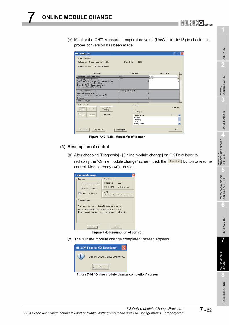
7 ONLINE MODULE CHANGE
1
OV
ER
VIE
W
2
SY
ST
EM
C
ON
FIG
UR
AT
ION
3
SP
EC
IFIC
AT
ION
S
4
SE
TU
P A
ND
P
RO
CE
DU
RE
S B
EF
OR
E
OP
ER
AT
ION
5
UT
ILIT
Y P
AC
KA
GE
(G
X
CO
NF
IGU
RA
TO
R-T
I)
6
PR
OG
RA
MM
ING
7
ON
LIN
E M
OD
ULE
C
HA
NG
E
8
TR
OU
BL
ES
HO
OT
ING
(e) Monitor the CH Measured temperature value (Un\G11 to Un\18) to check that
proper conversion has been made.
Figure 7.42 "CH Monitor/test" screen
(5) Resumption of control
(a) After choosing [Diagnosis] - [Online module change] on GX Developer to
redisplay the "Online module change" screen, click the button to resume
control. Module ready (X0) turns on.
Figure 7.43 Resumption of control
(b) The "Online module change completed" screen appears.
Figure 7.44 "Online module change completion" screen
7.3 Online Module Change Procedure7.3.4 When user range setting is used and initial setting was made with GX Configurator-TI (other system
7 - 22

7 ONLINE MODULE CHANGE
7.3.5 When user range setting is used and initial setting was made with sequence program (other system is available)
(1) Conversion disable
(a) Set conversion enable/disable setting (Un\G0) for all channel conversion disable
and turn Operating Condition Setting Request (Y9) from OFF to ON to stop
conversion.
After confirming that conversion has stopped with the Conversion Completion
Flag (Un\G10), turn off Operating Condition Setting Request (Y9).
Figure 7.45 "Device test" screen
(2) Dismounting of module
(a) After choosing [Diagnosis] - [Online module change] on GX Developer to enter the
"Online module change" mode, double-click the module to be changed online to
display the "Online module change" screen.]
Figure 7.46 "System Monitor" screen
7 - 23 7.3 Online Module Change Procedure7.3.5 When user range setting is used and initial setting was made with sequence program (other system

7 ONLINE MODULE CHANGE
1
OV
ER
VIE
W
2
SY
ST
EM
C
ON
FIG
UR
AT
ION
3
SP
EC
IFIC
AT
ION
S
4
SE
TU
P A
ND
P
RO
CE
DU
RE
S B
EF
OR
E
OP
ER
AT
ION
5
UT
ILIT
Y P
AC
KA
GE
(G
X
CO
NF
IGU
RA
TO
R-T
I)
6
PR
OG
RA
MM
ING
7
ON
LIN
E M
OD
ULE
C
HA
NG
E
8
TR
OU
BL
ES
HO
OT
ING
(b) Click the button to enable a module change.
Figure 7.47 "Online module change" screen
If the following error screen appears, the user range cannot be saved.
Click the button, and perform the operation in Section 7.3.6 (2)(c)
and later.
Figure 7.48 Error screen
(c) After confirming that the "RUN" LED of the module has turned off, remove the
connector and dismount the module.
POINTAlways dismount the module. If you execute mounting confirmation without
dismounting the module, the module will not start properly and the "RUN" LED will
not be lit.
7.3 Online Module Change Procedure7.3.5 When user range setting is used and initial setting was made with sequence program (other system
7 - 24

7 ONLINE MODULE CHANGE
(3) Mounting of new module
(a) Mount the dismounted module and new module to the other system.
(b) Using the G(P).OGLOAD instruction, save the user range setting values to the
CPU device. Refer to Appendix 2.3 for the G(P).OGLOAD instruction.
(c) Using the G(P).OGSTOR instruction, restore the user range setting set values to
the module. Refer to Appendix 2.4 for the G(P).OGSTOR instruction.
(d) Dismount a new module from the other system, mount it to the slot from where the
old module was dismounted in the original system, and install the connector.
(e) After mounting the module, click the button and make sure that the
"RUN" LED is lit. Module ready (X0) remains OFF.
Figure 7.49 "Online module change" screen
(4) Operation check
(a) To make an operation check, click the button to cancel control
resumption.
Figure 7.50 Cancel of control resumption
7 - 25 7.3 Online Module Change Procedure7.3.5 When user range setting is used and initial setting was made with sequence program (other system

7 ONLINE MODULE CHANGE
1
OV
ER
VIE
W
2
SY
ST
EM
C
ON
FIG
UR
AT
ION
3
SP
EC
IFIC
AT
ION
S
4
SE
TU
P A
ND
P
RO
CE
DU
RE
S B
EF
OR
E
OP
ER
AT
ION
5
UT
ILIT
Y P
AC
KA
GE
(G
X
CO
NF
IGU
RA
TO
R-T
I)
6
PR
OG
RA
MM
ING
7
ON
LIN
E M
OD
ULE
C
HA
NG
E
8
TR
OU
BL
ES
HO
OT
ING
(b) Click the button to leave the "Online module change" mode.
Figure 7.51 "Online module change"mode stop
(c) Click the button to close the System monitor screen.
Figure 7.52 "System Monitor" screen
(d) Enable the conversion of the channel to be used in Conversion enable/disable
setting (Un\G0), and turn Operating condition setting request (Y9) from OFF to
ON.
(e) Monitor CH Measured temperature value (Un\G11 to Un\G18) to check if the
conversion is processed normally.
(f) Since the new module is in a default status, it must be initialized by a sequence
program after control resumption.
Before performing initialization, check whether the contents of the initialization
program are correct or not.
1) Normal system configuration
The sequence program should perform initialization on the leading edge of
Module ready (X0) of the Q68TD-G-H02(H01).
When control resumption is executed, Module ready (X0) turns ON and
initialization is performed. (If the sequence program performs initialization only
one scan after RUN, initialization is not performed.)
2) When used on remote I/O network
Insert a user device that will execute initialization at any timing (initialization
request signal) into the sequence program. After control resumption, turn ON
the initialization request signal to perform initialization. (If the sequence
program performs initialization only one scan after a data link start of the
remote I/O network, initialization is not performed.)
7.3 Online Module Change Procedure7.3.5 When user range setting is used and initial setting was made with sequence program (other system
7 - 26

7 ONLINE MODULE CHANGE
(5) Resumption of control
(a) After choosing [Diagnosis] - [Online module change] on GX Developer to
redisplay the "Online module change" screen, click the button to resume
control. Module ready (X0) turns on.
Figure 7.53 Resumption of control
(b) The "Online module change completed" screen appears.
Figure 7.54 "Online module change completed" screen
7 - 27 7.3 Online Module Change Procedure7.3.5 When user range setting is used and initial setting was made with sequence program (other system

7 ONLINE MODULE CHANGE
1
OV
ER
VIE
W
2
SY
ST
EM
C
ON
FIG
UR
AT
ION
3
SP
EC
IFIC
AT
ION
S
4
SE
TU
P A
ND
P
RO
CE
DU
RE
S B
EF
OR
E
OP
ER
AT
ION
5
UT
ILIT
Y P
AC
KA
GE
(G
X
CO
NF
IGU
RA
TO
R-T
I)
6
PR
OG
RA
MM
ING
7
ON
LIN
E M
OD
ULE
C
HA
NG
E
8
TR
OU
BL
ES
HO
OT
ING
7.3.6 When user range setting is used and initial setting was made with sequence program (other system is unavailable)
(1) Conversion disable
(a) Set "Disable" in the conversion enable/disable setting (Un\G0) for all channels
and turn Operating Condition Setting Request (Y9) from OFF to ON to stop
conversion.
After confirming that conversion has stopped with the Conversion Completion
Flag (Un\G10), turn off Operating Condition Setting Request (Y9).
Figure 7.55 "Device test" screen
(b) If the saved buffer memory contents are not yet prerecorded, record them in the
following procedure.
1) Turn Operating Condition Setting Request (Y9) form OFF to ON.
2) Compare the current values of the following buffer memory with those of the
range reference table, make sure those are proper values.
Refer to Section 7.4 for the range reference table.
• CH Factory default offset value (Un\G190*1)
• CH Factory default gain value (Un\G191*1)
• CH User range settings offset value (Un\G192*1)
• CH User range settings gain value (Un\G193*1)
• CH User range settings thermal EMF offset value (Un\G194,Un\G195*1)
• CH User range settings thermal EMF gain value (Un\G196,Un\G197*1) * 1: Only the buffer memory address of channel 1 is given on the above.
Refer to the Section 3.4.1 Buffer memory assignment for the buffer memory address of other channels
3) Record the buffer memory values.
7.3 Online Module Change Procedure7.3.6 When user range setting is used and initial setting was made with sequence program (other system
7 - 28

7 ONLINE MODULE CHANGE
POINTIf the buffer memory values compared with the reference table are not proper,
save and restoration of the user range cannot be executed.
Before executing module control resumption, follow the flowchart in Section 4.6
and make offset/gain setting in the device test of GX Developer.
Perform mode switching by making the setting of the mode switching setting
(Un\G158, Un\G159) and turning Operating Condition Setting Request (Y9) from
OFF to ON.
Note that if module control is resumed without offset/gain setting being made,
operation will be performed with the default values.
(2) Dismounting of module
(a) After choosing [Diagnosis] - [Online module change] on GX Developer to enter the
"Online module change" mode, double-click the module to be changed online to
display the "Online module change" screen.
Figure 7.56 "System Monitor" screen
(b) Click the button to enable a module change.
Figure 7.57 "Online module change" screen
7 - 29 7.3 Online Module Change Procedure7.3.6 When user range setting is used and initial setting was made with sequence program (other system

7 ONLINE MODULE CHANGE
1
OV
ER
VIE
W
2
SY
ST
EM
C
ON
FIG
UR
AT
ION
3
SP
EC
IFIC
AT
ION
S
4
SE
TU
P A
ND
P
RO
CE
DU
RE
S B
EF
OR
E
OP
ER
AT
ION
5
UT
ILIT
Y P
AC
KA
GE
(G
X
CO
NF
IGU
RA
TO
R-T
I)
6
PR
OG
RA
MM
ING
7
ON
LIN
E M
OD
ULE
C
HA
NG
E
8
TR
OU
BL
ES
HO
OT
ING
If the following error screen appears, the user range cannot be saved. Click the
button, and perform the operation in Section 7.3.6 (2)(c) and later.
Figure 7.58 Error screen
(c) After confirming that the "RUN" LED of the module has turned off, remove the
connector and dismount the module.
POINTAlways dismount the module. If you execute mounting confirmation without
dismounting the module, the module will not start properly and the "RUN" LED will
not be lit.
(3) Mounting of new module
(a) Mount a new module to the same slot, and install the connector.
(b) After mounting the module, click the button and make sure that the
"RUN" LED is lit. Module ready (X0) remains OFF.
Figure 7.59 "Online module change" screen
7.3 Online Module Change Procedure7.3.6 When user range setting is used and initial setting was made with sequence program (other system
7 - 30

7 ONLINE MODULE CHANGE
(4) Operation check
(a) To make an operation check, click the button to cancel control
resumption.
Figure 7.60 Cancel of control resumption
(b) Click the button to leave the "Online module change" mode.
Figure 7.61 "Online module change" mode stop
(c) Click the button to close the System monitor screen.
Figure 7.62 "System Monitor" screen
(d) Choose [Online] - [Debug] - [Device test] on GX Developer and set the values
prerecorded in Section 7.3.6 (2) to the buffer memory.
(e) Turn the user range write request (YA) from OFF to ON to restore the user set
values to the module.
After confirming that the offset/gain setting mode status flag (XA) is ON, turn OFF
the user range write request (YA).
7 - 31 7.3 Online Module Change Procedure7.3.6 When user range setting is used and initial setting was made with sequence program (other system

7 ONLINE MODULE CHANGE
1
OV
ER
VIE
W
2
SY
ST
EM
C
ON
FIG
UR
AT
ION
3
SP
EC
IFIC
AT
ION
S
4
SE
TU
P A
ND
P
RO
CE
DU
RE
S B
EF
OR
E
OP
ER
AT
ION
5
UT
ILIT
Y P
AC
KA
GE
(G
X
CO
NF
IGU
RA
TO
R-T
I)
6
PR
OG
RA
MM
ING
7
ON
LIN
E M
OD
ULE
C
HA
NG
E
8
TR
OU
BL
ES
HO
OT
ING
(f) Enable the conversion of the channel to be used in Conversion enable/disable
setting (Un\G0), and turn Operating condition setting request (Y9) from OFF to
ON.
(g) Monitor CH Measured temperature value (Un\G11 to Un\G18) to check if the
conversion is processed normally.
(h) Since the new module is in a default status, it must be initialized by a sequence
program after control resumption.
Before performing initialization, check whether the contents of the initialization
program are correct or not.
1) Normal system configuration
The sequence program should perform initialization on the leading edge of
Module ready (X0) of the Q68TD-G-H02(H01).
When control resumption is executed, Module ready (X0) turns ON and
initialization is performed. (If the sequence program performs initialization only
one scan after RUN, initialization is not performed.)
2) When used on remote I/O network
Insert a user device that will execute initialization at any timing (initialization
request signal) into the sequence program. After control resumption, turn ON
the initialization request signal to perform initialization. (If the sequence
program performs initialization only one scan after a data link start of the
remote I/O network, initialization is not performed.)
(5) Resumption of control
(a) After choosing [Diagnosis] - [Online module change] on GX Developer to
redisplay the "Online module change" screen, click the button to resume
control. Module ready (X0) turns on.
Figure 7.63 Resumption of control
(b) The "Online module change completed" screen appears.
Figure 7.64 "Online module completed" screen
7.3 Online Module Change Procedure7.3.6 When user range setting is used and initial setting was made with sequence program (other system
7 - 32

7 ONLINE MODULE CHANGE
7.4 Range Reference Table
The range reference tables are given below.
7.4.1 Range reference table (Q68TD-G-H02)
(1) Compare the factory default offset value with the reference value F868H.
(2) Compare the factory default gain value with the reference value 3640H.
(3) Compare the user range settings offset value with the value obtained from the following expression.
(4) Compare the user range settings gain value with the value obtained from the following expression.
(5) Obtain a value that corresponds to the offset setting temperature set by the user from the chart of standard thermal electromotive force that is compliant with JIS C 1602-1995, IEC584-1, and IEC584-2. Compare the value with the user range settings offset thermal electromotive force value.
(6) Obtain a value that corresponds to the gain setting temperature set by the user from the chart of standard thermal electromotive force that is compliant with JIS C 1602-1995, IEC584-1, and IEC584-2. Compare the value with the user range settings gain thermal electromotive force value.
POINTThe chart of standard thermal electromotive force compliant with JIS C 1602-1995
and IEC584-1, or IEC584-2 needs to be arranged by the user.
Address (Decimal)Description Reference value
CH1 CH2 CH3 CH4 CH5 CH6 CH7 CH8
190 198 206 214 222 230 238 246 Factory default offset valueDigital value for offset value set prior to
shipment (Reference value F868H)
191 199 207 215 223 231 239 247 Factory default gain valueDigital value for gain value set prior to
shipment (Reference value 3640H)
192 200 208 216 224 232 240 248 User range settings offset valueDigital value for user-set offset value (Refer to
(3))
193 201 209 217 225 233 241 249 User range settings gain valueDigital value for user-set gain value (Refer to
(4))
194 202 210 218 226 234 242 250 User range settings thermal EMF offset value (L) Thermal EMF for user-set offset set
temperature ( V unit) (Refer to (5))195 203 211 219 227 235 243 251 User range settings thermal EMF offset value (H)
196 204 212 220 228 236 244 252 User range settings thermal EMF gain value (L) Thermal EMF for user-set gain set temperature
( V unit) (Refer to (6))197 205 213 221 229 237 245 253 User range settings thermal EMF gain value (H)
(Digital value) =User range settings thermal
EMF offset value ( V)45000 18515832
(Digital value) =User range settings thermal
EMF gain value ( V)15832 45000 185
7 - 33 7.4 Range Reference Table7.4.1 Range reference table (Q68TD-G-H02)

7 ONLINE MODULE CHANGE
1
OV
ER
VIE
W
2
SY
ST
EM
C
ON
FIG
UR
AT
ION
3
SP
EC
IFIC
AT
ION
S
4
SE
TU
P A
ND
P
RO
CE
DU
RE
S B
EF
OR
E
OP
ER
AT
ION
5
UT
ILIT
Y P
AC
KA
GE
(G
X
CO
NF
IGU
RA
TO
R-T
I)
6
PR
OG
RA
MM
ING
7
ON
LIN
E M
OD
ULE
C
HA
NG
E
8
TR
OU
BL
ES
HO
OT
ING
(Example)
When offset/gain setting is made at the offset set temperature of -200.0°C and the gain
set temperature of 900.0°C with an E type thermocouple connected
Value typeSet
temperature
Reference value of user range settings thermal
EMF offset/gain value
Reference value of user range settings offset/
gain value
Offset value - 200.0 - 8825( V) - 8825 15832 45000-185 =F326H
Gain value 900.0 68787( V) 68787 15832 45000-185 = 5DD0H
7.4 Range Reference Table7.4.1 Range reference table (Q68TD-G-H02)
7 - 34

7 ONLINE MODULE CHANGE
7.4.2 Range reference table (Q68TD-G-H01)
(1) Compare the factory default offset value with the reference value F89BH.
(2) Compare the factory default gain value with the reference value 3B22H.
(3) Compare the user range settings offset value with the value obtained from the following expression.
(4) Compare the user range settings gain value with the value obtained from the following expression.
(5) Obtain the chart of standard thermal electromotive force, complying with JIS C 1602-1995 and IEC584-1, or IEC584-2, for the user range settings offset thermal electromotive force value. Then, compare the value with the offset setting temperature set by the user.
(6) Obtain the chart of standard thermal electromotive force, complying with JIS C 1602-1995 and IEC584-1, or IEC584-2, for the user range settings gain thermal electromotive force value. Then, compare the value with the gain setting temperature set by the user.
POINTThe chart of standard thermal electromotive force compliant with JIS C 1602-1995
and IEC584-1, or IEC584-2 needs to be arranged by the user.
Address (Decimal)Description Reference value
CH1 CH2 CH3 CH4 CH5 CH6 CH7 CH8
190 198 206 214 222 230 238 246 Factory default offset valueDigital value for offset value set prior to
shipment (Reference value F89BH)
191 199 207 215 223 231 239 247 Factory default gain valueDigital value for gain value set prior to
shipment (Reference value 3B22H)
192 200 208 216 224 232 240 248 User range settings offset valueDigital value for user-set offset value (Refer to
(3))
193 201 209 217 225 233 241 249 User range settings gain valueDigital value for user-set gain value (Refer to
(4))
194 202 210 218 226 234 242 250 User range settings thermal EMF offset value (L) Thermal EMF for user-set offset set
temperature ( V unit) (Refer to (5))195 203 211 219 227 235 243 251 User range settings thermal EMF offset value (H)
196 204 212 220 228 236 244 252 User range settings thermal EMF gain value (L) Thermal EMF for user-set gain set temperature
( V unit) (Refer to (6))197 205 213 221 229 237 245 253 User range settings thermal EMF gain value (H)
(Digital value) =User range settings thermal
EMF offset value ( V)3276790909
(Digital value) =User range settings thermal
EMF gain value ( V)90909 32767
7 - 35 7.4 Range Reference Table7.4.2 Range reference table (Q68TD-G-H01)

7 ONLINE MODULE CHANGE
1
OV
ER
VIE
W
2
SY
ST
EM
C
ON
FIG
UR
AT
ION
3
SP
EC
IFIC
AT
ION
S
4
SE
TU
P A
ND
P
RO
CE
DU
RE
S B
EF
OR
E
OP
ER
AT
ION
5
UT
ILIT
Y P
AC
KA
GE
(G
X
CO
NF
IGU
RA
TO
R-T
I)
6
PR
OG
RA
MM
ING
7
ON
LIN
E M
OD
ULE
C
HA
NG
E
8
TR
OU
BL
ES
HO
OT
ING
(Example)
When offset/gain setting is made at the offset set temperature of -200.0°C and the gain
set temperature of 900.0°C with an E type thermocouple connected
Value typeSet
temperature
Reference value of user range settings thermal
EMF offset/gain value
Reference value of user range settings offset/
gain value
Offset value - 200.0 - 8825( V) - 8825 90909 32767=-3180
Gain value 900.0 68787( V) 68787 90909 32767= 24793
7.4 Range Reference Table7.4.2 Range reference table (Q68TD-G-H01)
7 - 36

7 - 37 7.5 Precautions for Online Module Change
7 ONLINE MODULE CHANGE
7.5 Precautions for Online Module Change
The following are the precautions for online module change.
(1) Always perform an online module change in the correct procedure. A failure to do so can cause a malfunction or failure.
(2) If an online module change is made with the user range setting, the accuracy after that will fall to about less than 1/3 of the accuracy before that.Re-set the offset/gain values as necessary.
(3) During an online module change, do not perform the operations below. If they are performed, the Q68TD-G-H02 (H01) may not operate normally.
(a) Powering off the programmable controller CPU
(b) Resetting the programmable controller CPU
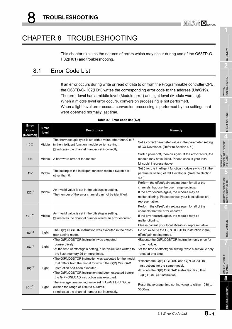
8 TROUBLESHOOTING
1
OV
ER
VIE
W
2
SY
ST
EM
C
ON
FIG
UR
AT
ION
3
SP
EC
IFIC
AT
ION
S
4
SE
TU
P A
ND
P
RO
CE
DU
RE
S B
EF
OR
E
OP
ER
AT
ION
5
UT
ILIT
Y P
AC
KA
GE
(G
X
CO
NF
IGU
RA
TO
R-T
I)
6
PR
OG
RA
MM
ING
7
ON
LIN
E M
OD
ULE
C
HA
NG
E
8
TR
OU
BL
ES
HO
OT
ING
CHAPTER 8 TROUBLESHOOTING
This chapter explains the natures of errors which may occur during use of the Q68TD-G-
H02(H01) and troubleshooting.
8.1 Error Code List
If an error occurs during write or read of data to or from the Programmable controller CPU,
the Q68TD-G-H02(H01) writes the corresponding error code to the address (Un\G19).
The error level has a middle level (Module error) and light level (Module warning).
When a middle level error occurs, conversion processing is not performed.
When a light level error occurs, conversion processing is performed by the settings that
were operated normally last time.
Table 8.1 Error code list (1/2)
Error
Code
(Decimal)
Error
levelDescription Remedy
10 Middle
The thermocouple type is set with a value other than 0 to 7
in the intelligent function module switch setting.
indicates the channel number set incorrectly.
Set a correct parameter value in the parameter setting
of GX Developer. (Refer to Section 4.5.)
111 Middle A hardware error of the module
Switch power off, then on again. If the error recurs, the
module may have failed. Please consult your local
Mitsubishi representative.
112 MiddleThe setting of the intelligent function module switch 5 is
other than 0.
Set 0 for the intelligent function module switch 5 in the
parameter setting of GX Developer. (Refer to Section
4.5.)
120*1 MiddleAn invalid value is set in the offset/gain setting.
The number of the error channel can not be identified.
Perform the offset/gain setting again for all of the
channels that use the user range settings.
If the error occurs again, the module may be
malfunctioning. Please consult your local Mitsubishi
representative.
12 *1 MiddleAn invalid value is set in the offset/gain setting.
indicates the channel number where an error occurred.
Perform the offset/gain setting again for all of the
channels that the error occurred.
If the error occurs again, the module may be
malfunctioning.
Please consult your local Mitsubishi representative.
161*2 LightThe G(P).OGSTOR instruction was executed in the offset/
gain setting mode.
Do not execute the G(P).OGSTOR instruction in the
offset/gain setting mode.
162*1 Light
•The G(P).OGSTOR instruction was executed
consecutively.
•At the time of offset/gain setting, a set value was written to
the flash memory 26 or more times.
•Execute the G(P).OGSTOR instruction only once for
one module.
•At the time of offset/gain setting, write a set value only
once at one time.
163*1 Light
•The G(P).OGSTOR instruction was executed for the model
that differs from the model for which the G(P).OGLOAD
instruction had been executed.
•The G(P).OGSTOR instruction had been executed before
the G(P).OGLOAD instruction was executed.
•Execute the G(P).OGLOAD and G(P).OGSTOR
instructions for the same model.
•Execute the G(P).OGLOAD instruction first, then
G(P).OGSTOR instruction.
20 *1 Light
The average time setting value set in Un\G1 to Un\G8 is
outside the range of 1280 to 5000ms.
indicates the channel number set incorrectly.
Reset the average time setting value to within 1280 to
5000ms.
8.1 Error Code List
8 - 1

8 TROUBLESHOOTING
Table 8.1 Error code list (2/2)
Error
Code
(Decimal)
Error
levelDescription Remedy
30 *1 Light
The averaging count setting value set in Un\G1 to Un\G8 is
outside the range of 4 to 500 times.
indicates the channel number set incorrectly.
Reset the average count setting value to within 4 to 500
times.
31 *1 Light
The moving average count setting value set in Un\G1 to Un\
G8 is outside the range of 2 to 60 times.
indicates the channel number set incorrectly.
Reset the moving average count setting value to within
2 to 60 times.
32 *1 Light
The time constant setting value for the primary delay filter
set in Un\G1 to Un\G8 is outside the range of 320 to
5000ms.
indicates the channel number set incorrectly.
Reset the time constant setting value to within 320 to
5000ms.
40 *1 Light(Gain value) - (Offset value) 0.1 [ ]
indicates the channel number where an error occurred.Check the voltage at the thermocouple input terminal.
41 *1 Light
(Gain temperature setting value) - (Offset temperature
setting value) 0.1 [ ]
indicates the channel number where an error occurred.
Reset the offset/gain temperature setting value (Un\
G28 to Un\G43) of the channel number where an error
occurred.
500*1 Light
The same channel or 0 is set to both the offset/gain setting
(Offset specification) (Un\G26) and offset/gain setting (Gain
specification) (Un\G27).
Reset the data of the offset/gain setting (Offset
specification) (Un\G26) and offset/gain setting (Gain
specification) (Un\G27).
51 *1 Light
When the channel change request (YB) is turned ON, the
setting status is in the following either status.
•The offset temperature setting value or gain temperature
setting value of the specified channel is set outside the
measured range.
•The disconnected channel or the channel for conversion
disable is specified.
indicates the channel number set incorrectly.
•Check the measurement range and reset the offset/
gain temperature setting value (Un\G28 to Un\G43)
within the range.
•Check wire disconnection or specify the channel for
conversion enable.
6 *1 Light
The process alarm upper/lower limit value (Un\G94 to Un\
G125) is set contradictorily.
indicates the channel number set incorrectly.
indicates the following status.
Reset the process alarm upper/lower limit value (Un\
G94 to Un\G125).
70 *1 Light
The rate alarm warning detection period (Un\G126 to Un\
G133) is outside the range of 1 to 6000 times
indicates the channel number set incorrectly.
Reset the rate alarm warning detection period (Un\
G126 to Un\G133) to within 1 to 6000 times.
800*1 MiddleWire disconnection of the cold junction temperature
compensation resistor (RTD) is detected.
Check wiring status of the cold junction temperature
compensation resistor (RTD).
91 *1 Light
The setting value in the scaling range upper/lower limit
value (Un\G62 to Un\G77) or scaling width upper/lower limit
value (Un\G78 to Un\G93) indicates that (Lower limit) =
(Upper limit).
indicates the channel number set incorrectly.
Reset the scaling range upper/lower limit value (Un\
G62 to Un\G77) or scaling width upper/lower limit value
(Un\G78 to Un\G93).
0: The lower lower limit value is lower than the
measurement range.
1: The upper upper limit value is higher than the
measurement range.
2: (Lower lower limit value) > (Lower upper limit value)
3: (Lower upper limit value) > (Upper lower limit value)
4: (Upper lower limit value) > (Upper upper limit value)
8 - 2 8.1 Error Code List

8 TROUBLESHOOTING
1
OV
ER
VIE
W
2
SY
ST
EM
C
ON
FIG
UR
AT
ION
3
SP
EC
IFIC
AT
ION
S
4
SE
TU
P A
ND
P
RO
CE
DU
RE
S B
EF
OR
E
OP
ER
AT
ION
5
UT
ILIT
Y P
AC
KA
GE
(G
X
CO
NF
IGU
RA
TO
R-T
I)
6
PR
OG
RA
MM
ING
7
ON
LIN
E M
OD
ULE
C
HA
NG
E
8
TR
OU
BL
ES
HO
OT
ING
POINT(1) The code of the first error found by the Q68TD-G-H02(H01) is stored when
two or more errors occur.
(2) The error codes marked with *1 can be cleared by turning ON the error clear
request (YF).
(3) The error code161 marked by *2 can not stored in the error code (Un\G19).
It is stored in the completion status area (S)+1 of the G(P).OGSTOR
instruction.
8.1 Error Code List
8 - 3

8 TROUBLESHOOTING
8.2 Troubleshooting
8.2.1 "RUN" LED is extinguished
8.2.2 "RUN" LED flickers
8.2.3 "ERR" LED flickers
8.2.4 "ERR" LED is lit
Table 8.2 "RUN" LED is extinguished
Check Item Remedy
Check that power is supplied.Confirm that the supply voltage of the power supply module
is within the rated range.
Check that the capacity of the power supply module is
sufficient.
Calculate the current consumption of the CPU, I/O, intelligent
function and other modules loaded on the base unit, and
make sure that the power supply capacity is enough.
Check for a watchdog timer error.
Reset the programmable controller CPU and verify that it is
lit. If the "RUN" LED does not light even after doing this, the
module may be malfunctioning. Please consult your local
Mitsubishi representative.
Check whether the modules are loaded normally on the base
unit.Check the module loading status.
Is a module change enabled during an online module
change?Refer to CHAPTER 7 and take corrective action.
Table 8.3 "RUN" LED flickers
Check Item Remedy
Check whether the module is in the offset/gain setting mode
or not.
Reset the switch 4 in the intelligent function module switch
setting of GX Developer to set to the normal mode. (Refer to
Section 4.5)
Table 8.4 "ERR" LED flickers
Check Item Remedy
Check whether the switch 5 of the intelligent function module
switches is "other than 0".
Set 0 for the switch 5 of the intelligent function module switch
setting of GX Developefor. (Refer to Section 4.5)
Table 8.5 "ERR" LED is lit
Check Item Remedy
Check for an error.Check the error code and take the action given in Section
8.1.
8 - 4 8.2 Troubleshooting8.2.1 "RUN" LED is extinguished
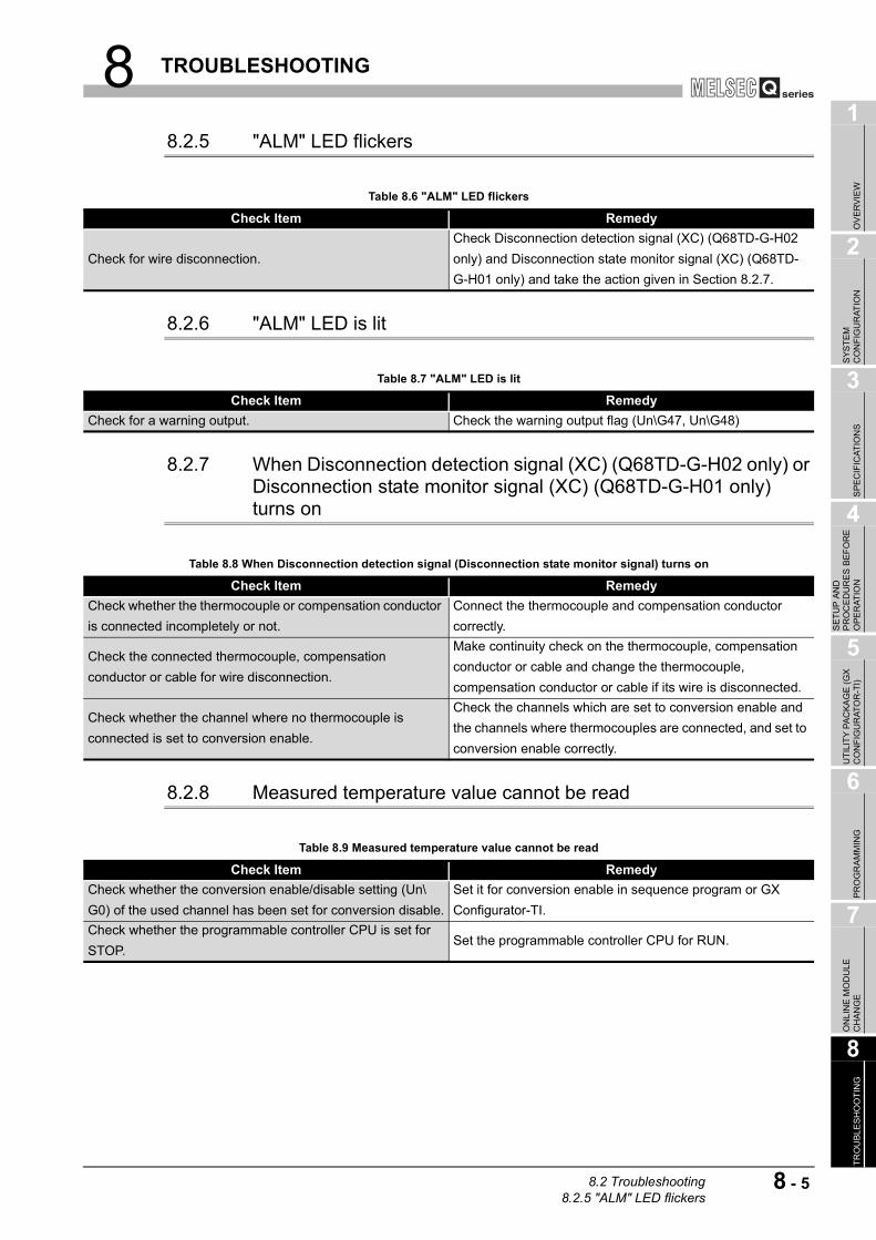
8 TROUBLESHOOTING
1
OV
ER
VIE
W
2
SY
ST
EM
C
ON
FIG
UR
AT
ION
3
SP
EC
IFIC
AT
ION
S
4
SE
TU
P A
ND
P
RO
CE
DU
RE
S B
EF
OR
E
OP
ER
AT
ION
5
UT
ILIT
Y P
AC
KA
GE
(G
X
CO
NF
IGU
RA
TO
R-T
I)
6
PR
OG
RA
MM
ING
7
ON
LIN
E M
OD
ULE
C
HA
NG
E
8
TR
OU
BL
ES
HO
OT
ING
8.2.5 "ALM" LED flickers
8.2.6 "ALM" LED is lit
8.2.7 When Disconnection detection signal (XC) (Q68TD-G-H02 only) or Disconnection state monitor signal (XC) (Q68TD-G-H01 only) turns on
8.2.8 Measured temperature value cannot be read
Table 8.6 "ALM" LED flickers
Check Item Remedy
Check for wire disconnection.
Check Disconnection detection signal (XC) (Q68TD-G-H02
only) and Disconnection state monitor signal (XC) (Q68TD-
G-H01 only) and take the action given in Section 8.2.7.
Table 8.7 "ALM" LED is lit
Check Item Remedy
Check for a warning output. Check the warning output flag (Un\G47, Un\G48)
Table 8.8 When Disconnection detection signal (Disconnection state monitor signal) turns on
Check Item Remedy
Check whether the thermocouple or compensation conductor
is connected incompletely or not.
Connect the thermocouple and compensation conductor
correctly.
Check the connected thermocouple, compensation
conductor or cable for wire disconnection.
Make continuity check on the thermocouple, compensation
conductor or cable and change the thermocouple,
compensation conductor or cable if its wire is disconnected.
Check whether the channel where no thermocouple is
connected is set to conversion enable.
Check the channels which are set to conversion enable and
the channels where thermocouples are connected, and set to
conversion enable correctly.
Table 8.9 Measured temperature value cannot be read
Check Item Remedy
Check whether the conversion enable/disable setting (Un\
G0) of the used channel has been set for conversion disable.
Set it for conversion enable in sequence program or GX
Configurator-TI.
Check whether the programmable controller CPU is set for
STOP.Set the programmable controller CPU for RUN.
8.2 Troubleshooting8.2.5 "ALM" LED flickers
8 - 5

8 TROUBLESHOOTING
8.2.9 Measured temperature value is abnormal
POINTThe module may be faulty if the measured temperature values cannot be read
after proper corrective actions have been taken according to the above check
items. Please consult your local Mitsubishi representative.
Table 8.10 Measured temperature value is abnormal
Check Item Remedy
Check whether the connected thermocouple or
compensation conductor differs from the setting.
Set the thermocouple type connected to the switch 1 or 2 in
the intelligent function module switch setting of GX
Developer.
Check whether the connected thermocouple or
compensation conductor is connected reversely.
Connect the thermocouple or compensation conductor
correctly.
Check the wiring.Refer to Section 4.4.2 (1) Wiring procedure, and wire cables
and compensating lead wires correctly.
Check for noise in the thermocouple input.Check influence from the ground and adjacent devices, and
take action to prevent noise.
Check the cold junction temperature compensation resistor
(RTD) for making cold junction temperature compensation for
wire disconnection or disconnection from the relay terminal
block.
Check that the cold junction temperature compensation
resistor (RTD) is connected to the relay terminal block and
there is continuity, and if not, connect or change the cold
junction temperature compensation resistor (RTD).
Check whether the cold junction temperature compensation
yes/no setting is correct.
Set the switch 4 to the correct position in the intelligent
function module switch setting of GX Developer. (Refer to
Section 4.5.)
Check whether conversion is made with the other
thermocouple set after setting of the offset/gain value
Make offset/gain setting again after changing the
thermocouple.
Check whether wiring between the module and terminal
block is correct.
Check that wiring between the module and terminal block is
performed correctly.
The Q68TD-G-H01 module was mounted in the limited
position in the system using the power supply module of the
Q63P, Q63RP, Q64P or Q64RP.
Refer to Section 2.1 (2) Restrictions on mountable slot
position in which the module can be installed.
Check whether the effect of temperature error due to wiring
resistance of a thermocouple is large.
Check the wiring resistance value of the thermocouple and
calculate the temperature error in the system. (Refer to
Section 3.1(2))
If the error is large, it may cause a change of the measured
temperature value. Correct the measured temperature value
by the offset/gain setting. (Refer to Section 4.6.)
8 - 6 8.2 Troubleshooting8.2.9 Measured temperature value is abnormal

8 TROUBLESHOOTING
1
OV
ER
VIE
W
2
SY
ST
EM
C
ON
FIG
UR
AT
ION
3
SP
EC
IFIC
AT
ION
S
4
SE
TU
P A
ND
P
RO
CE
DU
RE
S B
EF
OR
E
OP
ER
AT
ION
5
UT
ILIT
Y P
AC
KA
GE
(G
X
CO
NF
IGU
RA
TO
R-T
I)
6
PR
OG
RA
MM
ING
7
ON
LIN
E M
OD
ULE
C
HA
NG
E
8
TR
OU
BL
ES
HO
OT
ING
8.2.10 Checking the Q68TD-G-H02(H01) status using GX Developer system monitor
When the Q68TD-G-H02(H01) detail information is selected in GX Developer system
monitor, error code can be checked.
(1) Operating GX Developer[Diagnostics] [System monitor] Select "Q68TD-G-H01" or "Q68TD-G-H02"
(2) Module Detail Information
(a) Checking the function version and product information
The function version and product information of the Q68TD-G-H02(H01) is
displayed in the product information field.
(b) Checking the error code
The error code stored in the error code (Un\G19) of the Q68TD-G-H02(H01) is
displayed in the Present Error field.
(When the button is pressed, the contents displayed in the Present
Error field are displayed in the No. 1 field.)
Figure 8.1 Module detail information screen (Q68TD-G-H02 only)
Function version
Product information
(First 5 digits)
8.2 Troubleshooting8.2.10 Checking the Q68TD-G-H02(H01) status using GX Developer system monitor
8 - 7

8 TROUBLESHOOTING
(3) H/W information
(a) H/W LED information
The LED ON status is displayed.
(b) H/W SW information
The status of the intelligent function module switch setting is displayed.
Figure 8.2 H/W information screen
Table 8.11 LED ON status
No. LED name Status
1 RUN LED 0000H : Indicates that LED is unlit.
0001H : Indicates that LED is lit
Alternate indication between 0000H and 0001H: Indicates that
LED flickers
2 ERR. LED
3 ALM LED
Table 8.12 Switch setting status for intelligent function module
No. Switch setting for intelligent function module
RANGE1 Switch 1
RANGE2 Switch 2
RANGE3 Switch 3
MODE Switch 4
- Switch 5
8 - 8 8.2 Troubleshooting8.2.10 Checking the Q68TD-G-H02(H01) status using GX Developer system monitor
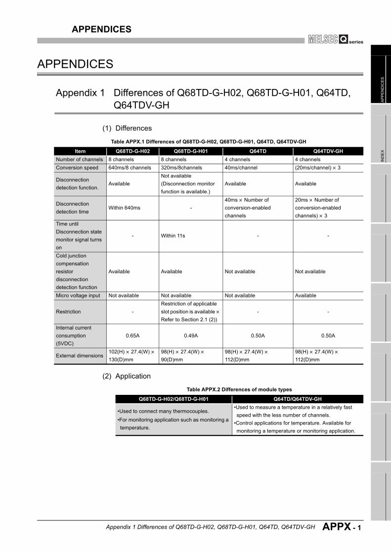
APPENDICES
AP
PE
ND
ICE
SIN
DE
X
APPENDICES
Appendix 1 Differences of Q68TD-G-H02, Q68TD-G-H01, Q64TD, Q64TDV-GH
(1) Differences
(2) Application
Table APPX.1 Differences of Q68TD-G-H02, Q68TD-G-H01, Q64TD, Q64TDV-GH
Item Q68TD-G-H02 Q68TD-G-H01 Q64TD Q64TDV-GH
Number of channels 8 channels 8 channels 4 channels 4 channels
Conversion speed 640ms/8 channels 320ms/8channels 40ms/channel (20ms/channel) 3
Disconnection
detection function.Available
Not available
(Disconnection monitor
function is available.)
Available Available
Disconnection
detection timeWithin 640ms -
40ms Number of
conversion-enabled
channels
20ms Number of
conversion-enabled
channels) 3
Time until
Disconnection state
monitor signal turns
on
- Within 11s - -
Cold junction
compensation
resistor
disconnection
detection function
Available Available Not available Not available
Micro voltage input Not available Not available Not available Available
Restriction -
Restriction of applicable
slot position is available
Refer to Section 2.1 (2))
- -
Internal current
consumption
(5VDC)
0.65A 0.49A 0.50A 0.50A
External dimensions102(H) 27.4(W)
130(D)mm
98(H) 27.4(W)
90(D)mm
98(H) 27.4(W)
112(D)mm
98(H) 27.4(W)
112(D)mm
Table APPX.2 Differences of module types
Q68TD-G-H02/Q68TD-G-H01 Q64TD/Q64TDV-GH
•Used to connect many thermocouples.
•For monitoring application such as monitoring a
temperature.
•Used to measure a temperature in a relatively fast
speed with the less number of channels.
•Control applications for temperature. Available for
monitoring a temperature or monitoring application.
Appendix 1 Differences of Q68TD-G-H02, Q68TD-G-H01, Q64TD, Q64TDV-GH
APPX - 1

APPENDICES
Appendix 2 Dedicated Instruction
Appendix 2.1 Dedicated Instruction List and Available Device
(1) Dedicated instruction listThe following table lists the dedicated instructions that can be used with the Q68TD-
G-H02(H01) converter modules.
POINTWhen the module is mounted to a MELSECNET/H remote station, the dedicated
instructions cannot be used.
(2) Available devicesThe following devices are available for the dedicated instructions:
* 1 Word device bit designation can be used as bit data.
Word device bit designation is done by designating , .
(Designation of bit numbers is done in hexadecimal.)
For example, bit 10 of D0 is designated as .
However, there can be no bit designation for timers (T), retentive timers (ST) and counters (C).
Table APPX.3 Dedicated instruction list
Instruction DescriptionReference
section
G(P).OFFGANSwitches to the offset/gain setting mode.
Switches to the normal mode.Appendix 2.2
G(P).OGLOADReads the offset/gain values of the user range setting to
the CPU.Appendix 2.3
G(P).OGSTOR
Restores the offset/gain values of the user range setting
stored in the CPU to the Q68TD-G-H02(H01) converter
module.
Appendix 2.4
Table APPX.4 Available devices
Internal devicesFile register Constant
Bit*1 Word
X, Y, M, L, F, V, B T, ST, C, D, W R, ZR -
Word device Bit No.
D0.A
APPX - 2 Appendix 2 Dedicated InstructionAppendix 2.1 Dedicated Instruction List and Available Device
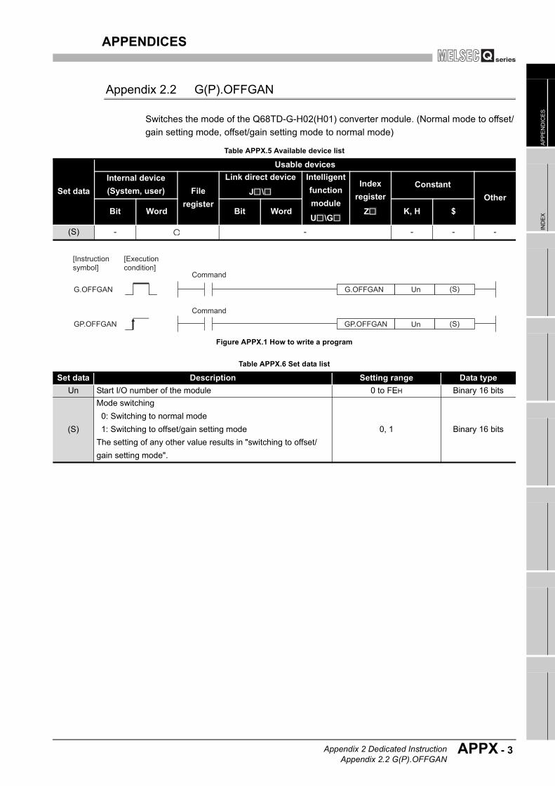
APPENDICES
AP
PE
ND
ICE
SIN
DE
X
Appendix 2.2 G(P).OFFGAN
Switches the mode of the Q68TD-G-H02(H01) converter module. (Normal mode to offset/
gain setting mode, offset/gain setting mode to normal mode)
Figure APPX.1 How to write a program
Table APPX.5 Available device list
Set data
Usable devices
Internal device
(System, user) File
register
Link direct device
J \
Intelligent
function
module
U \G
Index
register
Z
Constant
Other
Bit Word Bit Word K, H $
(S) - - - - -
Table APPX.6 Set data list
Set data Description Setting range Data type
Un Start I/O number of the module 0 to FEH Binary 16 bits
(S)
Mode switching
0: Switching to normal mode
1: Switching to offset/gain setting mode
The setting of any other value results in "switching to offset/
gain setting mode".
0, 1 Binary 16 bits
G.OFFGAN
GP.OFFGAN
G.OFFGAN Un
GP.OFFGAN Un
[Instruction
symbol]
[Execution
condition]Command
Command
(S)
(S)
Appendix 2 Dedicated InstructionAppendix 2.2 G(P).OFFGAN
APPX - 3

APPENDICES
(1) FunctionSwitches the mode of the Q68TD-G-H02(H01) converter module
• Normal mode to offset/gain setting mode (the offset/gain setting mode status flag
(XA) turns ON)
• Offset/gain setting mode to normal mode (the offset/gain setting mode status flag
(XA) turns OFF)
POINT(1) When the offset/gain setting mode is switched to the normal mode, Module
ready (X0) turns from OFF to ON.
Note that initial setting processing will be executed if there is a sequence
program that makes initial setting when Module ready (X0) turns ON.
(2) When the normal mode is switched to the offset/gain setting mode, all
channels set to temperature conversion disable.
Set the channels where offset/gain setting will be made for conversion enable
and turn ON the operating condition setting request (Y9).
(3) When the offset/gain setting mode is switched to the normal mode, restore
the normal mode status prior to switching to the offset/gain setting mode and
start temperature conversion.
(2) Operation errorNo errors.
(3) Program exampleThe following program is designed to switch the Q68TD-G-H02(H01) converter
module mounted in the position of I/O number X/Y0 to X/YF to the offset/gain setting
mode when M10 is turned ON, and to return it to the normal mode when M10 is turned
OFF.
Figure APPX.2 Program example
Dedicated instruction
(G.OFFGAN)
Dedicated instruction
(G.OFFGAN)
Stores "1: Switching to
offset/gain setting mode".
Stores "0: Switching to
normal mode".
Switching to offset/gain setting mode
Switching to normal mode
Processing of offset/gain mode setting
Processing in normal mode
APPX - 4 Appendix 2 Dedicated InstructionAppendix 2.2 G(P).OFFGAN

APPENDICES
AP
PE
ND
ICE
SIN
DE
X
Appendix 2.3 G(P).OGLOAD
Reads the offset/gain values of the user range setting of the Q68TD-G-H02(H01)
converter module to the CPU.
Figure APPX.3 How to write a program
Table APPX.7 Available device List
Set data
Usable devices
Internal device
(System, user) File
register
Link direct device
J \
Intelligent
function
module
U \G
Index
register
Z
Constant
Other
Bit Word Bit Word K, H $
(S) - - - - -
(D) - - - -
Table APPX.8 Set data list
Set data Description Setting range Data type
Un Start I/O number of the module 0 to FEH Binary 16 bits
(S) Start number of the device in which control data is stored.Within the range of the
specified deviceDevice name
(D)
Device that is turned ON 1 scan on completion of dedicated
instruction processing.
(D) + 1 also turns ON at an abnormal completion.
Within the range of the
specified deviceBit
G.OGLOADG.OGLOAD
GP.OGLOAD
Un (D)
(D)
(S)
(S)UnGP.OGLOAD
[Instruction
symbol]
[Execution
condition]Command
Command
Appendix 2 Dedicated InstructionAppendix 2.3 G(P).OGLOAD
APPX - 5

APPENDICES
* 1 Setting is not necessary. If setting is made, the offset/gain values will not be read properly.
Table APPX.9 Control data (1/2)*1
Device Item Set data Setting range Set by
(S) System area - - -
(S) + 1 Completion status
Stores the status when the instruction
is complete.
0 : Normal completion
Other than 0: Abnormal completion
- System
(S) + 2System area - - -
(S) + 3
(S) + 4 CH1 Factory default offset value - - System
(S) + 5 CH1 Factory default gain value - - System
(S) + 6 CH1 User range settings offset value - - System
(S) + 7 CH1 User range settings gain value - - System
(S) + 8 CH1 User range settings thermal EMF offset value (L) - - System
(S) + 9 CH1 User range settings thermal EMF offset value (H) - - System
(S) + 10 CH1 User range settings thermal EMF gain value (L) - - System
(S) + 11 CH1 User range settings thermal EMF gain value (H) - - System
(S) + 12 CH2 Factory default offset value - - System
(S) + 13 CH2 Factory default gain value - - System
(S) + 14 CH2 User range settings offset value - - System
(S) + 15 CH2 User range settings gain value - - System
(S) + 16 CH2 User range settings thermal EMF offset value (L) - - System
(S) + 17 CH2 User range settings thermal EMF offset value (H) - - System
(S) + 18 CH2 User range settings thermal EMF gain value (L) - - System
(S) + 19 CH2 User range settings thermal EMF gain value (H) - - System
(S) + 20 CH3 Factory default offset value - - System
(S) + 21 CH3 Factory default gain value - - System
(S) + 22 CH3 User range settings offset value - - System
(S) + 23 CH3 User range settings gain value - - System
(S) + 24 CH3 User range settings thermal EMF offset value (L) - - System
(S) + 25 CH3 User range settings thermal EMF offset value (H) - - System
(S) + 26 CH3 User range settings thermal EMF gain value (L) - - System
(S) + 27 CH3 User range settings thermal EMF gain value (H) - - System
(S) + 28 CH4 Factory default offset value - - System
(S) + 29 CH4 Factory default gain value - - System
(S) + 30 CH4 User range settings offset value - - System
(S) + 31 CH4 User range settings gain value - - System
(S) + 32 CH4 User range settings thermal EMF offset value (L) - - System
(S) + 33 CH4 User range settings thermal EMF offset value (H) - - System
(S) + 34 CH4 User range settings thermal EMF gain value (L) - - System
(S) + 35 CH4 User range settings thermal EMF gain value (H) - - System
APPX - 6 Appendix 2 Dedicated InstructionAppendix 2.3 G(P).OGLOAD

APPENDICES
AP
PE
ND
ICE
SIN
DE
X
* 1 Setting is not necessary. If setting is made, the offset/gain values will not be read properly.
Table APPX.9 Control data (2/2)*1
Device Item Set data Setting range Set by
(S) + 36 CH5 Factory default offset value - - System
(S) + 37 CH5 Factory default gain value - - System
(S) + 38 CH5 User range settings offset value - - System
(S) + 39 CH5 User range settings gain value - - System
(S) + 40 CH5 User range settings thermal EMF offset value (L) - - System
(S) + 41 CH5 User range settings thermal EMF offset value (H) - - System
(S) + 42 CH5 User range settings thermal EMF gain value (L) - - System
(S) + 43 CH5 User range settings thermal EMF gain value (H) - - System
(S) + 44 CH6 Factory default offset value - - System
(S) + 45 CH6 Factory default gain value - - System
(S) + 46 CH6 User range settings offset value - - System
(S) + 47 CH6 User range settings gain value - - System
(S) + 48 CH6 User range settings thermal EMF offset value (L) - - System
(S) + 49 CH6 User range settings thermal EMF offset value (H) - - System
(S) + 50 CH6 User range settings thermal EMF gain value (L) - - System
(S) + 51 CH6 User range settings thermal EMF gain value (H) - - System
(S) + 52 CH7 Factory default offset value - - System
(S) + 53 CH7 Factory default gain value - - System
(S) + 54 CH7 User range settings offset value - - System
(S) + 55 CH7 User range settings gain value - - System
(S) + 56 CH7 User range settings thermal EMF offset value (L) - - System
(S) + 57 CH7 User range settings thermal EMF offset value (H) - - System
(S) + 58 CH7 User range settings thermal EMF gain value (L) - - System
(S) + 59 CH7 User range settings thermal EMF gain value (H) - - System
(S) + 60 CH8 Factory default offset value - - System
(S) + 61 CH8 Factory default gain value - - System
(S) + 62 CH8 User range settings offset value - - System
(S) + 63 CH8 User range settings gain value - - System
(S) + 64 CH8 User range settings thermal EMF offset value (L) - - System
(S) + 65 CH8 User range settings thermal EMF offset value (H) - - System
(S) + 66 CH8 User range settings thermal EMF gain value (L) - - System
(S) + 67 CH8 User range settings thermal EMF gain value (H) - - System
Appendix 2 Dedicated InstructionAppendix 2.3 G(P).OGLOAD
APPX - 7

APPENDICES
(1) Functions
(a) Reads the offset/gain values of the user range setting of the Q68TD-G-H02(H01)
converter module to the CPU.
(b) There are two types of interlock signals for the G(P).OGLOAD instruction: the
completion device (D) and the status display device at completion (D) + 1.
1) Completion device
Turns ON in the END processing of the scan where the G(P).OGLOAD
instruction is completed, and turns OFF in the next END processing.
2) Status display device at completion
Turns ON and OFF depending on the completion status of the G(P).OGLOAD
instruction.
Figure APPX.4 Timing diagram
(2) Operation errorNo errors.
(3) Program exampleThe following program is designed to read the offset/gain values of the Q68TD-G-
H02(H01) converter module mounted in the position of I/O number X/Y0 to X/YF when
M11 is turned ON.
Figure APPX.5 Program example
Normal completion : Stays OFF and does not change.
Abnormal completion: Turns ON in the END processing of the scan where the
G(P).OGLOAD instruction is completed, and turns OFF
in the next END processing.
ON
OFF
OFF
OFF
ON
Sequence program
G(P).OGLOAD instruction
Completion device (D)
Status display device
at completion (D)+1
END processing END processing END processing END processing
Execution completion of
the G(P).OGLOAD instruction
ON Abnormal
completion
Normal completion
1 scan
Dedicated instruction
(GP.OGLOAD)
Setting control data
Reading offset/gain satting values
Processing at the time of error completion
APPX - 8 Appendix 2 Dedicated InstructionAppendix 2.3 G(P).OGLOAD

APPENDICES
AP
PE
ND
ICE
SIN
DE
X
Appendix 2.4 G(P).OGSTOR
Restores the offset/gain values of the user range setting stored in the CPU to the Q68TD-
G-H02(H01) converter module.
Figure APPX.6 How to write a program
* 1 When executing the G.OGLOAD instruction, specify the device designated in (S).Do not change the data read with the G.OGLOAD instruction.If it is changed, normal operation cannot be guaranteed.
Table APPX.10 Available device List
Set data
Usable devices
Internal device
(System, user) File
register
Link direct device
J \
Intelligent
function
module
U \G
Index
register
Z
Constant
Other
Bit Word Bit Word K, H $
(S) - - - - -
(D) - - - -
Table APPX.11 Set data list
Set data Description Setting range Data type
Un Start I/O number of the module 0 to FEH Binary 16 bits
(S)*1 Start number of the device in which control data is stored.Within the range of the
specified deviceDevice name
(D)
Device that is turned ON 1 scan on completion of dedicated
instruction processing.
(D) + 1 also turns ON at an abnormal completion.
Within the range of the
specified deviceBit
G.OGSTOR
[Instruction
symbol][Execution
condition]
G.OGSTOR
GP.OGSTOR
Command
Command
G.OGSTOR Un (S) (D)
GP.OGSTOR Un (S) (D)
Appendix 2 Dedicated InstructionAppendix 2.4 G(P).OGSTOR
APPX - 9

APPENDICES
Table APPX.12 Control data (1/2)
Device Item Set data Setting range Set by
(S) System area - - -
(S) + 1 Completion status
Stores the status when the instruction
is complete.
0 : Normal completion
Other than 0: Abnormal completion
- System
(S) + 2System area - - -
(S) + 3
(S) + 4 CH1 Factory default offset value - - System
(S) + 5 CH1 Factory default gain value - - System
(S) + 6 CH1 User range settings offset value - - System
(S) + 7 CH1 User range settings gain value - - System
(S) + 8 CH1 User range settings thermal EMF offset value (L) - - System
(S) + 9 CH1 User range settings thermal EMF offset value (H) - - System
(S) + 10 CH1 User range settings thermal EMF gain value (L) - - System
(S) + 11 CH1 User range settings thermal EMF gain value (H) - - System
(S) + 12 CH2 Factory default offset value - - System
(S) + 13 CH2 Factory default gain value - - System
(S) + 14 CH2 User range settings offset value - - System
(S) + 15 CH2 User range settings gain value - - System
(S) + 16 CH2 User range settings thermal EMF offset value (L) - - System
(S) + 17 CH2 User range settings thermal EMF offset value (H) - - System
(S) + 18 CH2 User range settings thermal EMF gain value (L) - - System
(S) + 19 CH2 User range settings thermal EMF gain value (H) - - System
(S) + 20 CH3 Factory default offset value - - System
(S) + 21 CH3 Factory default gain value - - System
(S) + 22 CH3 User range settings offset value - - System
(S) + 23 CH3 User range settings gain value - - System
(S) + 24 CH3 User range settings thermal EMF offset value (L) - - System
(S) + 25 CH3 User range settings thermal EMF offset value (H) - - System
(S) + 26 CH3 User range settings thermal EMF gain value (L) - - System
(S) + 27 CH3 User range settings thermal EMF gain value (H) - - System
(S) + 28 CH4 Factory default offset value - - System
(S) + 29 CH4 Factory default gain value - - System
(S) + 30 CH4 User range settings offset value - - System
(S) + 31 CH4 User range settings gain value - - System
(S) + 32 CH4 User range settings thermal EMF offset value (L) - - System
(S) + 33 CH4 User range settings thermal EMF offset value (H) - - System
(S) + 34 CH4 User range settings thermal EMF gain value (L) - - System
(S) + 35 CH4 User range settings thermal EMF gain value (H) - - System
APPX - 10 Appendix 2 Dedicated InstructionAppendix 2.4 G(P).OGSTOR

APPENDICES
AP
PE
ND
ICE
SIN
DE
X
Table APPX.12 Control data (2/2)
Device Item Set data Setting range Set by
(S) + 36 CH5 Factory default offset value - - System
(S) + 37 CH5 Factory default gain value - - System
(S) + 38 CH5 User range settings offset value - - System
(S) + 39 CH5 User range settings gain value - - System
(S) + 40 CH5 User range settings thermal EMF offset value (L) - - System
(S) + 41 CH5 User range settings thermal EMF offset value (H) - - System
(S) + 42 CH5 User range settings thermal EMF gain value (L) - - System
(S) + 43 CH5 User range settings thermal EMF gain value (H) - - System
(S) + 44 CH6 Factory default offset value - - System
(S) + 45 CH6 Factory default gain value - - System
(S) + 46 CH6 User range settings offset value - - System
(S) + 47 CH6 User range settings gain value - - System
(S) + 48 CH6 User range settings thermal EMF offset value (L) - - System
(S) + 49 CH6 User range settings thermal EMF offset value (H) - - System
(S) + 50 CH6 User range settings thermal EMF gain value (L) - - System
(S) + 51 CH6 User range settings thermal EMF gain value (H) - - System
(S) + 52 CH7 Factory default offset value - - System
(S) + 53 CH7 Factory default gain value - - System
(S) + 54 CH7 User range settings offset value - - System
(S) + 55 CH7 User range settings gain value - - System
(S) + 56 CH7 User range settings thermal EMF offset value (L) - - System
(S) + 57 CH7 User range settings thermal EMF offset value (H) - - System
(S) + 58 CH7 User range settings thermal EMF gain value (L) - - System
(S) + 59 CH7 User range settings thermal EMF gain value (H) - - System
(S) + 60 CH8 Factory default offset value - - System
(S) + 61 CH8 Factory default gain value - - System
(S) + 62 CH8 User range settings offset value - - System
(S) + 63 CH8 User range settings gain value - - System
(S) + 64 CH8 User range settings thermal EMF offset value (L) - - System
(S) + 65 CH8 User range settings thermal EMF offset value (H) - - System
(S) + 66 CH8 User range settings thermal EMF gain value (L) - - System
(S) + 67 CH8 User range settings thermal EMF gain value (H) - - System
Appendix 2 Dedicated InstructionAppendix 2.4 G(P).OGSTOR
APPX - 11

APPENDICES
(1) Functions
(a) Restores the offset/gain values of the user range setting stored in the CPU to the
Q68TD-G-H02(H01) converter module.
(b) There are two types of interlock signals for the G(P).OGSTOR instruction: the
completion device (D) and the status display device at completion (D) + 1.
1) Completion device
Turns ON in the END processing of the scan where the G(P).OGSTOR
instruction is completed, and turns OFF in the next END processing.
2) Status display device at completion
Turns ON and OFF depending on the completion status of the G(P).OGSTOR
instruction.
Figure APPX.7 Timing diagram * 1 When the G(P).OGSTOR instruction is executed, conversion is not performed. After the
completion device (D) turns ON, conversion starts, the conversion value is stored into the buffer memory, and the conversion completion flag (XE) turns ON.
(c) When the offset/gain values are restored, the reference accuracy falls to about
less than 1/3 times of the previous accuracy.
(2) Operation errorIn any of the following cases, an error occurs and the corresponding error code is
stored into the completion status area (S)+1.
Normal completion : Stays OFF and does not change.
Abnormal completion: Turns ON in the END processing of the scan where the
G(P).OGLOAD instruction is completed, and turns OFF
in the next END processing.
Table APPX.13 Dedicated instruction error list
Error code Case resulting in operation error
161The G(P).OGSTOR instruction was executed in the offset/gain
setting mode.
162 The G(P).OGSTOR instruction was executed consecutively.
163
The G(P).OGSTOR instruction was executed for the model that
differs from the model for which the G(P).OGLOAD instruction had
been executed.
OFF
OFF
OFF
ON
OFF
Sequence program
G(P).OGSTOR instruction
Completion device (D)
Status display device
at completion (D)+1
Conversion
completion flag (XE)
END processing END processing END processing END processing
Execution completion of
the G(P).OGSTOR instruction
ON
ON
ON
ON Abnormal completion
Normal completion
1 scan
*1
APPX - 12 Appendix 2 Dedicated InstructionAppendix 2.4 G(P).OGSTOR
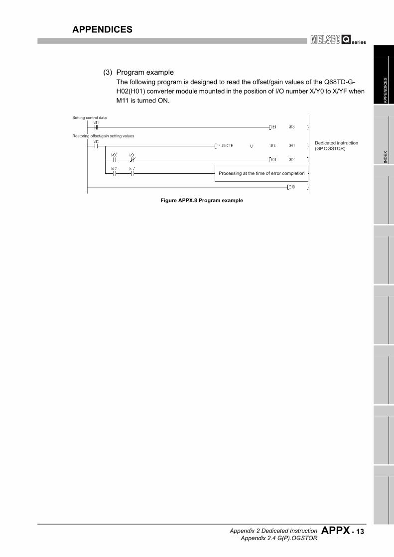
APPENDICES
AP
PE
ND
ICE
SIN
DE
X
(3) Program exampleThe following program is designed to read the offset/gain values of the Q68TD-G-
H02(H01) converter module mounted in the position of I/O number X/Y0 to X/YF when
M11 is turned ON.
Figure APPX.8 Program example
Dedicated instruction
(GP.OGSTOR)
Processing at the time of error completion
Setting control data
Restoring offset/gain setting values
Appendix 2 Dedicated InstructionAppendix 2.4 G(P).OGSTOR
APPX - 13

APPX - 14 Appendix 3 External Dimension Diagram
APPENDICES
Appendix 3 External Dimension Diagram
(1) Q68TD-G-H02
unit: mm
(2) Q68TD-G-H01
unit: mm
130
102
47 27.4
232
90
137
47
984
27.4
23

AP
PE
ND
ICE
SIN
DE
X
INDEX
[A]
About use of the Q68TD-G-H02 (H01) with the Q12PRH/Q25PRHCPU ......................................... 2-4Accuracy................................................................ 3-1Applicable systems................................................ 2-1Auto refresh settings............................................ 5-15Averaging processing ............................................ 3-8Averaging processing selection........................... 3-43
[B]
Buffer memory ..................................................... 3-30Buffer memory assignment.................................. 3-30
[C]
Channel change completion flag ......................... 3-25Channel change request ..................................... 3-29Checking the Q68TD-G-H02(H01) status using GX Developer system monitor..................................... 8-7Cold junction compensation setting status .......... 3-45Cold junction temperature compensation resistor disconnection detection function ......................... 3-21Cold junction temperature compensation with/without setting .................................................................. 4-19Common utility package operations ...................... 5-7Compatibility with online module change .............. 2-3Conversion completion flag ......................... 3-27,3-40Conversion enable/disable setting....................... 3-38Conversion setting for disconnection detection ... 3-59Conversion setting for disconnection detection function (Q68TD-G-H02 only).............................. 3-12Conversion setting value for disconnection detection............................................................................. 3-61Conversion setting value for disconnection state............................................................................. 3-61Conversion speed............................................ 3-1,3-7
[D]
Dedicated instruction ......................................APPX-2Dedicated instruction list and available device........................................................................APPX-2Differences of Q68TD-G-H02, Q68TD-G-H01, Q64TD, Q64TDV-GH .....................................APPX-1Disconnection detection flag................................ 3-48Disconnection detection signal ............................ 3-25Disconnection state conversion setting ............... 3-60Disconnection state conversion setting function (Q68TD-G-H01 only) ........................................... 3-14Disconnection state monitor flag ......................... 3-50Disconnection state monitor signal...................... 3-25Down scale .......................................................... A-12
[E]
EMC..................................................................... A-11Error clear request............................................... 3-29
Error code ............................................................ 3-42Error code list......................................................... 8-1Error Flag............................................................. 3-27External dimension diagram .........................APPX-14External wiring ....................................................... 4-8
[F]
Factory default offset/gain values, user range settings offset/gain values................................................. 3-62Features................................................................. 1-2Fixing module with module fixing bracket .............. 4-2Function list............................................................ 3-5
[G]
GX Configurator-TI ................................................ 2-3GX Developer ........................................................ 2-3G(P).OFFGAN ................................................APPX-3G(P).OGLOAD................................................APPX-5G(P).OGSTOR................................................APPX-9
[H]
Handling precautions ....................................... 4-1,5-3How to check the function version, product information and software version.............................................. 2-5
[I]
Initial setting......................................................... 5-13Installing and uninstalling the utility package......... 5-3Isolation specifications........................................... 3-1I/O signal details .................................................. 3-23I/O signal list ........................................................ 3-22
[L]
Low voltage directives .........................................A-11
[M]
Measured temperature value............................... 3-41Measured temperature value cannot be read........ 8-5Measured temperature value is abnormal ............. 8-6Mode switching setting ........................................ 3-58Module ready ....................................................... 3-23Monitoring/test ..................................................... 5-17Monitor/test screen .............................................. 5-17Moving average ..................................................... 3-9
[N]
Number of analog input points............................... 3-1Number of channels............................................... 3-1Number of I/O points occupied .............................. 3-1
[O]
Offset/gain setting................................................ 4-13Offset/gain setting mode...................................... 3-44
INDEX - 1

Offset/gain setting mode status flag .................... 3-24Offset/gain setting operation................................ 5-20Offset/gain temperature setting values ................ 3-45OMC (online module change) refresh data ......... 5-23Online module change........................................... 7-1Online module change conditions ......................... 7-2Online module change operations ......................... 7-3Online module change procedure ......................... 7-4Operating condition setting request ..................... 3-28Operating environment .......................................... 5-5Operation condition setting completion flag......... 3-23Operation overview................................................ 5-9Overview................................................................ 1-1
[P]
Part names ............................................................ 4-4Performance specifications ................................... 3-1Precautions for online module change ................ 7-37Primary delay filter ............................................... 3-10Process alarm...................................................... 3-16Process alarm upper/lower limit values ............... 3-56Product lineup......................................................A-14Program example when Configurator-TI ............... 6-8Program example when GX Configurator-TI is not used............................................................. 6-13,6-24Program example when GX Configurator-TI is used............................................................................. 6-20Programming ......................................................... 6-1Programming procedure ........................................ 6-2
[Q]
Q68TD-G-H01 .....................................................A-12Q68TD-G-H02 .....................................................A-12Q68TD-G-H02(H01) ............................................A-12
[R]
Range reference table (Q68TD-G-H01) .............. 7-35Range reference table (Q68TD-G-H02) .............. 7-33Rate alarm ........................................................... 3-17Rate alarm upper/lower limit values .................... 3-57Rate alarm warning detection period ................... 3-57Restrictions on mountable slot position ................. 2-1
[S]
Sampling period............................................... 3-1,3-7Sampling processing ............................................. 3-7Scaling range upper/lower limit values ................ 3-54Scaling valid/invalid setting.................................. 3-53Scaling value ....................................................... 3-52Scaling width upper/lower limit values ................. 3-55Setting range 1, 2 ................................................ 3-42Setting range 3 .................................................... 3-42Setup and procedures before operation .......... 4-1,4-3Starting the intelligent function module utility ...... 5-11Support of the multiple CPU system...................... 2-3Supported software packages ............................... 2-3Switch setting for intelligent function module....... 4-11System configuration ............................................. 2-1
[T]
Temperature conversion system ........................... 3-7Thermocouple compliance standards.................... 3-1Time/count/moving average/time constant setting............................................................................. 3-39Troubleshooting ............................................... 8-1,8-4
[U]
Up scale ...............................................................A-12User range write request ..................................... 3-28Using programs in normal system configuration.... 6-4Using programs on remote I/O network ............... 6-17Utility package (GX Configurator-TI)...................... 5-1Utility package functions ........................................ 5-1Utility package operation ....................................... 5-7
[W]
Warning output enable/disable setting................. 3-46Warning output flag.............................................. 3-47Warning output function....................................... 3-16Warning output signal .......................................... 3-26When factory default is used and initial setting was made with GX Configurator-TI ............................... 7-4When factory default is used and initial setting was made with sequence program ............................... 7-9When user range setting is used and initial setting was made with GX Configurator-TI (other system is available) ............................................................. 7-13When user range setting is used and initial setting was made with GX Configurator-TI (other system is unavailable) ......................................................... 7-18When user range setting is used and initial setting was made with sequence program (other system is available) ............................................................. 7-23When user range setting is used and initial setting was made with sequence program (other system is unavailable) ......................................................... 7-28Wiring..................................................................... 4-7Wiring precautions ................................................. 4-7
Symbols
"ALM" LED flickers................................................. 8-5"ALM" LED is lit...................................................... 8-5"ERR" LED flickers................................................. 8-4"ERR" LED is lit...................................................... 8-4"RUN" LED flickers ................................................ 8-4"RUN" LED is extinguished.................................... 8-4
INDEX - 2
WARRANTYPlease confirm the following product warranty details before using this product.
1. Gratis Warranty Term and Gratis Warranty RangeIf any faults or defects (hereinafter "Failure") found to be the responsibility of Mitsubishi occurs during use of the product within the gratis warranty term, the product shall be repaired at no cost via the sales representative or Mitsubishi Service Company.However, if repairs are required onsite at domestic or overseas location, expenses to send an engineer will be solely at the customer's discretion. Mitsubishi shall not be held responsible for any re-commissioning, maintenance, or testing on-site that involves replacement of the failed module.[Gratis Warranty Term]The gratis warranty term of the product shall be for one year after the date of purchase or delivery to a designated place.Note that after manufacture and shipment from Mitsubishi, the maximum distribution period shall be six (6) months, and the longest gratis warranty term after manufacturing shall be eighteen (18) months. The gratis warranty term of repair parts shall not exceed the gratis warranty term before repairs.[Gratis Warranty Range](1) The range shall be limited to normal use within the usage state, usage methods and usage environment, etc., which
follow the conditions and precautions, etc., given in the instruction manual, user's manual and caution labels on the product.
(2) Even within the gratis warranty term, repairs shall be charged for in the following cases.1. Failure occurring from inappropriate storage or handling, carelessness or negligence by the user. Failure caused
by the user's hardware or software design.2. Failure caused by unapproved modifications, etc., to the product by the user.3. When the Mitsubishi product is assembled into a user's device, Failure that could have been avoided if functions
or structures, judged as necessary in the legal safety measures the user's device is subject to or as necessary by industry standards, had been provided.
4. Failure that could have been avoided if consumable parts (battery, backlight, fuse, etc.) designated in the instruction manual had been correctly serviced or replaced.
5. Failure caused by external irresistible forces such as fires or abnormal voltages, and Failure caused by force majeure such as earthquakes, lightning, wind and water damage.
6. Failure caused by reasons unpredictable by scientific technology standards at time of shipment from Mitsubishi.7. Any other failure found not to be the responsibility of Mitsubishi or that admitted not to be so by the user.
2. Onerous repair term after discontinuation of production(1) Mitsubishi shall accept onerous product repairs for seven (7) years after production of the product is discontinued.
Discontinuation of production shall be notified with Mitsubishi Technical Bulletins, etc.(2) Product supply (including repair parts) is not available after production is discontinued.
3. Overseas serviceOverseas, repairs shall be accepted by Mitsubishi's local overseas FA Center. Note that the repair conditions at each FA Center may differ.
4. Exclusion of loss in opportunity and secondary loss from warranty liabilityRegardless of the gratis warranty term, Mitsubishi shall not be liable for compensation to:(1) Damages caused by any cause found not to be the responsibility of Mitsubishi.(2) Loss in opportunity, lost profits incurred to the user by Failures of Mitsubishi products.(3) Special damages and secondary damages whether foreseeable or not, compensation for accidents, and
compensation for damages to products other than Mitsubishi products.(4) Replacement by the user, maintenance of on-site equipment, start-up test run and other tasks.
5. Changes in product specificationsThe specifications given in the catalogs, manuals or technical documents are subject to change without prior notice.

Microsoft, Windows, Windows Vista, Windows NT, Windows XP, Windows Server, Visio, Excel, PowerPoint,
Visual Basic, Visual C++, and Access are either registered trademarks or trademarks of Microsoft Corporation in
the United States, Japan, and other countries.
Intel, Pentium, and Celeron are either registered trademarks or trademarks of Intel Corporation in the United
States and other countries.
Ethernet is a trademark of Xerox Corp.
All other company names and product names used in this manual are either trademarks or registered trade-
marks of their respective companies.
SPREAD
Copyright(C) 1996 FarPoint Technologies,Inc.
SH(NA)-080795ENG-D


SH-080795ENG-D(1606)MEEMODEL: Q68TD-G-H02-U-SY-EMODEL CODE: 13JZ26
Specifications subject to change without notice.
When exported from Japan, this manual does not require application to theMinistry of Economy, Trade and Industry for service transaction permission.
HEAD OFFICE : TOKYO BUILDING, 2-7-3 MARUNOUCHI, CHIYODA-KU, TOKYO 100-8310, JAPANNAGOYA WORKS : 1-14 , YADA-MINAMI 5-CHOME , HIGASHI-KU, NAGOYA , JAPAN


