118
1

1
2
Chapter 1 ...................................... 5
1.1 General Description ........................ 5
1.2 Key Features ................................... 6
1.3 Block Diagram ................................. 7
Chapter 2 ........................ 10
Board Components ............................. 10
2.1 Board Overview ............................. 10
2.2 Configuration, Status and Setup ..... 11
2.3 General User Input/Output ............ 14
2.4 Temperature Sensor and Fan Control
............................................................ 18
2.5 Power Monitor ............................... 20
2.6 Clock Circuit .................................. 21
2.7 FLASH Memory ............................. 23
2.8 DDR3 SO-DIMM ........................... 26
2.9 QDRII+ SRAM ............................... 36
2.10 QSPF+ Ports ............................... 45
2.11 PCI Express ................................ 48
2-12 RS-422 Expansion Header.......... 51
3
Chapter 3 ........................ 53
System Builder .................................... 53
3.1 Introduction ................................. 53
3.2 General Design Flow ..................... 54
3.3 Using System Builder .................... 55
Chapter 4 ........................ 61
Flash Programming ............................. 61
4.1 CFI Flash Memory Map ................. 61
4.2 FPGA Configure Operation............ 62
4.3 Flash Programming with Users Design
............................................................ 63
4.4 Restore Factory Settings ............... 64
Chapter 5 ........................ 65
Peripheral Reference Design .............. 65
5.1 Configure Si5340A/B in RTL ......... 66
5.2 Nios II control for
SI5340/Temperature/Power ................. 74
5.3 Fan Speed Control ........................ 79
4
Chapter 6 ........................ 82
Memory Reference Design .................. 82
6.1 QDRII+ SRAM Test ....................... 82
6.2 DDR3 SDRAM Test ....................... 85
6.3 DDR3 SDRAM Test by Nios II ....... 87
Chapter 7 ........................ 91
PCI Express Reference Design ........... 91
7.1 PCI Express System Infrastructure 91
7.2 PC PCI Express Software SDK ..... 92
PCI Express Software Stack ............... 93
7.3 PCIe Reference Design -
Fundamental ..................................... 101
7.4 PCIe Reference Design – DDR3 . 108
Chapter 8 ...................... 114
Transceiver Verification ...................... 114
8.1 Function of the Transceiver Test Code
........................................................... 114
8.2 Loopback Fixture .......................... 114
8.3 Testing.......................................... 116
Additional Information ........................ 118
Getting Help ....................................... 118
5
Chapter 1
Overview
his chapter provides an overview of the DE5a-Net Development Board and
installation guide.
1.1 General Description
The Terasic DE5a-Net Arria 10 GX FPGA Development Kit provides the ideal hardware
solution for designs that demand high capacity and bandwidth memory interfacing, ultra-
low latency communication, and power efficiency. With a full-height, 3/4-length form-
factor package, the DE5a-Net is designed for the most demanding high-end
applications, empowered with the top-of-the-line Altera Arria 10 GX, delivering the best
system-level integration and flexibility in the industry.
The Arria® 10 GX FPGA features integrated transceivers that transfer at a maximum of
12.5 Gbps, allowing the DE5a-Net to be fully compliant with version 3.0 of the PCI
Express standard, as well as allowing an ultra low-latency, straight connections to four
external 40G QSFP+ modules. Not relying on an external PHY will accelerate
mainstream development of network applications enabling customers to deploy designs
for a broad range of high-speed connectivity applications. For designs that demand high
capacity and high speed for memory and storage, the DE5a-Net delivers with two
independent banks of DDR3 SO-DIMM RAM, four independent banks of QDRII+ SRAM,
high-speed parallel flash memory. The feature-set of the DE5a-Net fully supports all
high-intensity applications such as low-latency trading, cloud computing, high-
performance computing, data acquisition, network processing, and signal processing.
T
6
1.2 Key Features
The following hardware is implemented on the DE5a-Net board:
FPGA
Altera Arria® 10 GX FPGA (10AX115N3F45I2SG)
FPGA Configuration
On-Board USB Blaster II or JTAG header for FPGA programming
Fast passive parallel (FPPx32) configuration via MAX II CPLD and flash memory
General user input/output:
8 LEDs
4 push-buttons
2 slide switches
2 seven-segment displays
Clock System
50MHz Oscillator
Programmable clock generators Si5340A and Si5340B
One SMA connector for external clock input
One SMA connector for clock output
Memory
DDR3 SO-DIMM SDRAM
QDRII+ SRAM
FLASH
Communication Ports
Four QSFP+ connectors
PCI Express (PCIe) x8 edge connector
One RS422 transceiver with RJ45 connector
System Monitor and Control
Temperature sensor
Fan control
Power monitor
7
Power
PCI Express 6-pin power connector, 12V DC Input
PCI Express edge connector power
Mechanical Specification
PCI Express full-height and 3/4-length
1.3 Block Diagram
Figure 1-1 shows the block diagram of the DE5a-Net board. To provide maximum
flexibility for the users, all key components are connected with the Arria 10 GX FPGA
device. Thus, users can configure the FPGA to implement any system design.
Figure 1-1 Block diagram of the DE5a-Net board
Below is more detailed information regarding the blocks in Figure 1-1.
8
Arria 10 GX FPGA
10AX115N3F45I2SG
1,150K logic elements (LEs)
67-Mbits embedded memory
48 transceivers (12.5Gbps)
3,036 18-bit x 19-bit multipliers
1,518 Variable-precision DSP blocks
4 PCI Express hard IP blocks
768 user I/Os
384 LVDS channels
32 phase locked loops (PLLs)
JTAG Header and FPGA Configuration
On-board USB Blaster II or JTAG header for use with the Quartus II
Programmer
MAXII CPLD 5M2210 System Controller and Fast Passive Parallel (FPP x32)
configuration
Memory devices
32MB QDRII+ SRAM
Up to 8GB DDR3 SO-DIMM SDRAM for each DDR3 socket
256MB FLASH
General user I/O
8 user controllable LEDs
4 user push buttons
2 user slide switches
2 seven-segment displays
9
On-Board Clock
50MHz oscillator
Programming PLL providing clock for 40G QSFP+ transceiver
Programming PLL providing clock for PCIe transceiver
Programming PLL providing clocks for DDR3 SDRAM and QDRII+ SRAM
Four QSFP+ ports
Four QSFP+ connector (40 Gbps+)
PCI Express x8 edge connector
Support for PCIe x8 Gen1/2/3
Edge connector for PC motherboard with x8 or x16 PCI Express slot
Power Source
PCI Express 6-pin DC 12V power
PCI Express edge connector power
10
Chapter 2
Board Components
his chapter introduces all the important components on the DE5a-Net.
2.1 Board Overview
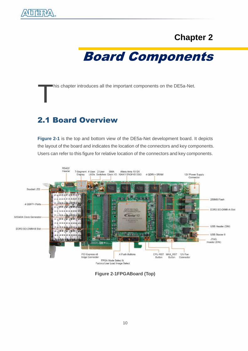
Figure 2-1 is the top and bottom view of the DE5a-Net development board. It depicts
the layout of the board and indicates the location of the connectors and key components.
Users can refer to this figure for relative location of the connectors and key components.
Figure 2-1FPGABoard (Top)
T

11
Figure 2-2 FPGA Board (Bottom)
2.2 Configuration, Status and Setup
Configure
The FPGA board supports two configuration methods for the Arria 10 FPGA:
Configure the FPGA using the on-board USB-Blaster II.
Flash memory configuration of the FPGA using stored images from the flash
memory on power-up.
For programming by on-board USB-Blaster II, the following procedures show how to
download a configuration bit stream into the Arria 10 GX FPGA:
Make sure that power is provided to the FPGA board
Connect your PC to the FPGA board using a mini-USB cable and make sure
the USB-Blaster II driver is installed on PC.
Launch Quartus II programmer and make sure the USB-Blaster II is detected.
In Quartus II Programmer, add the configuration bit stream file (.sof), check
the associated “Program/Configure” item, and click “Start” to start FPGA
programming.
12
Status LED
The FPGA Board development board includes board-specific status LEDs to indicate
board status. Please refer toTable 2-1for the description of the LED indicator.
Table 2-1 Status LED
Board
Reference LED Name Description
D6 12-V Power Illuminates when 12-V power is active.
D5 3.3-V Power Illuminates when 3.3-V power is active.
D16 CONF DONE
Illuminates when the FPGA is successfully
configured. Driven by the MAX II CPLD 5M2210
System Controller.
D15 Loading
Illuminates when the MAX II CPLD 5M2210 System
Controller is actively configuring the FPGA. Driven
by the MAX II CPLD 5M2210 System Controller
with the Embedded Blaster CPLD.
D17 Error
Illuminates when the MAX II CPLD EPM2210
System Controller fails to configure the FPGA.
Driven by the MAX II CPLD EPM2210 System
Controller.
D19 PAGE Illuminates when FPGA is configured by the factory
configuration bit stream.
Setup PCI Express Control DIP switch
The PCI Express Control DIP switch (SW5) is provided to enable or disable different
configurations of the PCIe Connector. Table 2-2lists the switch controls and description.
Table 2-2 SW5 PCIe Control DIP Switch
Board
Reference Signal Name Description Default
SW5.1 PCIE_PRSNT2n_x1 On : Enable x1 presence detect
Off: Disable x1 presence detect Off
SW5.2 PCIE_PRSNT2n_x4 On : Enable x4 presence detect
Off: Disable x4 presence detect Off
SW5.3 PCIE_PRSNT2n_x8 On : Enable x8 presence detect
Off: Disable x8 presence detect On
13
Setup Configure Mode
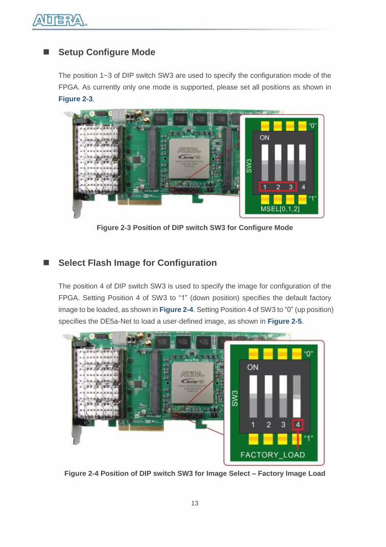
The position 1~3 of DIP switch SW3 are used to specify the configuration mode of the
FPGA. As currently only one mode is supported, please set all positions as shown in
Figure 2-3.
Figure 2-3 Position of DIP switch SW3 for Configure Mode
Select Flash Image for Configuration
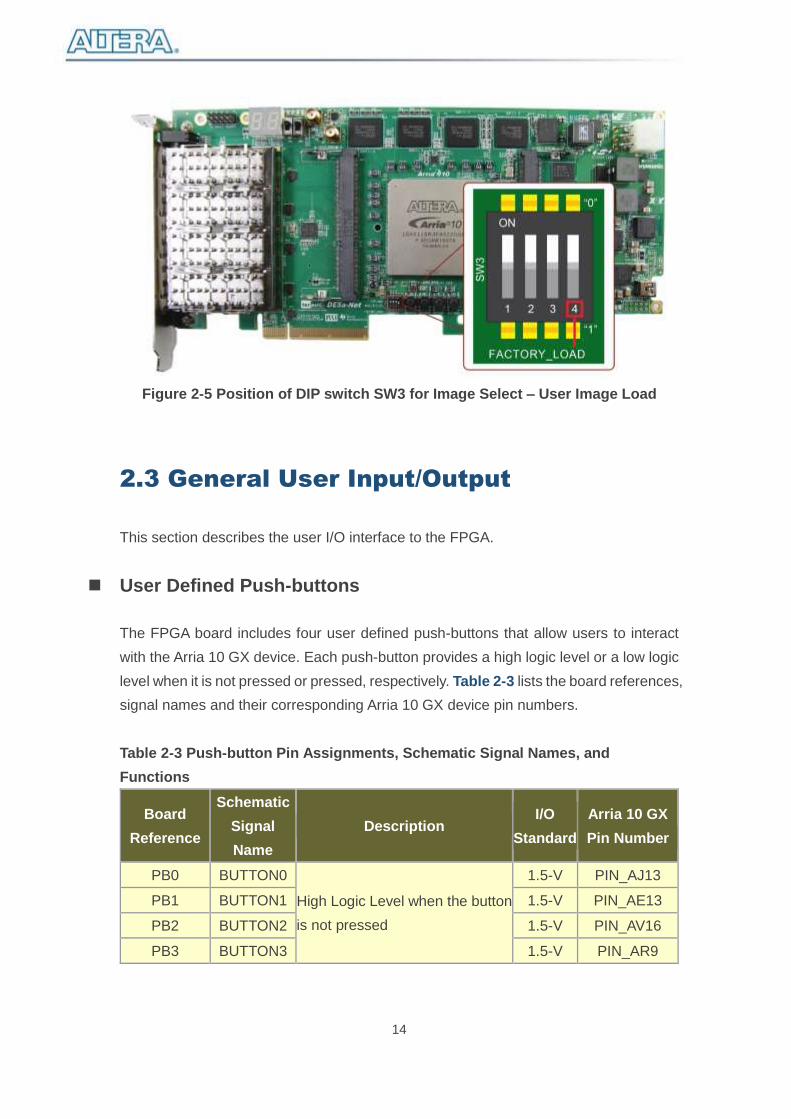
The position 4 of DIP switch SW3 is used to specify the image for configuration of the
FPGA. Setting Position 4 of SW3 to “1” (down position) specifies the default factory
image to be loaded, as shown in Figure 2-4. Setting Position 4 of SW3 to “0” (up position)
specifies the DE5a-Net to load a user-defined image, as shown in Figure 2-5.
Figure 2-4 Position of DIP switch SW3 for Image Select – Factory Image Load
14
Figure 2-5 Position of DIP switch SW3 for Image Select – User Image Load
2.3 General User Input/Output
This section describes the user I/O interface to the FPGA.
User Defined Push-buttons
The FPGA board includes four user defined push-buttons that allow users to interact
with the Arria 10 GX device. Each push-button provides a high logic level or a low logic
level when it is not pressed or pressed, respectively. Table 2-3 lists the board references,
signal names and their corresponding Arria 10 GX device pin numbers.
Table 2-3 Push-button Pin Assignments, Schematic Signal Names, and
Functions
Board
Reference
Schematic
Signal
Name
Description I/O
Standard
Arria 10 GX
Pin Number
PB0 BUTTON0
High Logic Level when the button
is not pressed
1.5-V PIN_AJ13
PB1 BUTTON1 1.5-V PIN_AE13
PB2 BUTTON2 1.5-V PIN_AV16
PB3 BUTTON3 1.5-V PIN_AR9

15
User-Defined Slide Switch
There are two slide switches on the FPGA board to provide additional FPGA input
control. When a slide switch is in the DOWN position or the UPPER position, it provides
a low logic level or a high logic level to the Arria 10 GX FPGA, respectively, as shown
in Figure 2-6.
Figure 2-6 4 Slide switches
Table 2-4 lists the signal names and their corresponding Arria 10 GX device pin
numbers.
Table 2-4 Slide Switch Pin Assignments, Schematic Signal Names, and
Functions
Board
Reference
Schematic
Signal Name Description
I/O
Standard
Arria 10 GX
Pin Number
SW0 SW0 High logic level when SW in the
UPPER position.
1.5-V PIN_AY28
SW1 SW1 1.5-V PIN_AM27
User-Defined LEDs
The FPGA board consists of 8 user-controllable LEDs to allow status and debugging
signals to be driven to the LEDs from the designs loaded into the Arria 10 GX device.
Each LED is driven directly by the Arria 10 GX FPGA. The LED is turned on or off when
16
the associated pins are driven to a low or high logic level, respectively. A list of the pin
names on the FPGA that are connected to the LEDs is given in Table 2-5.
Table 2-5 User LEDs Pin Assignments, Schematic Signal Names, and Functions
Board
Reference
Schematic
Signal Name Description
I/O
Standard
Arria 10 GX
Pin Number
D4 LED0
Driving a logic 0 on the I/O port
turns the LED ON.
Driving a logic 1 on the I/O port
turns the LED OFF.
1.8-V PIN_T11
D3 LED1 1.8-V PIN_R11
D2 LED2 1.8-V PIN_N15
D1 LED3 1.8-V PIN_M15
D9-1 LED_BRACKET0 1.8-V PIN_AF10
D9-3 LED_BRACKET1 1.8-V PIN_AF9
D9-5 LED_BRACKET2 1.8-V PIN_Y13
D9-7 LED_BRACKET3 1.8-V PIN_W11
7-Segment Displays
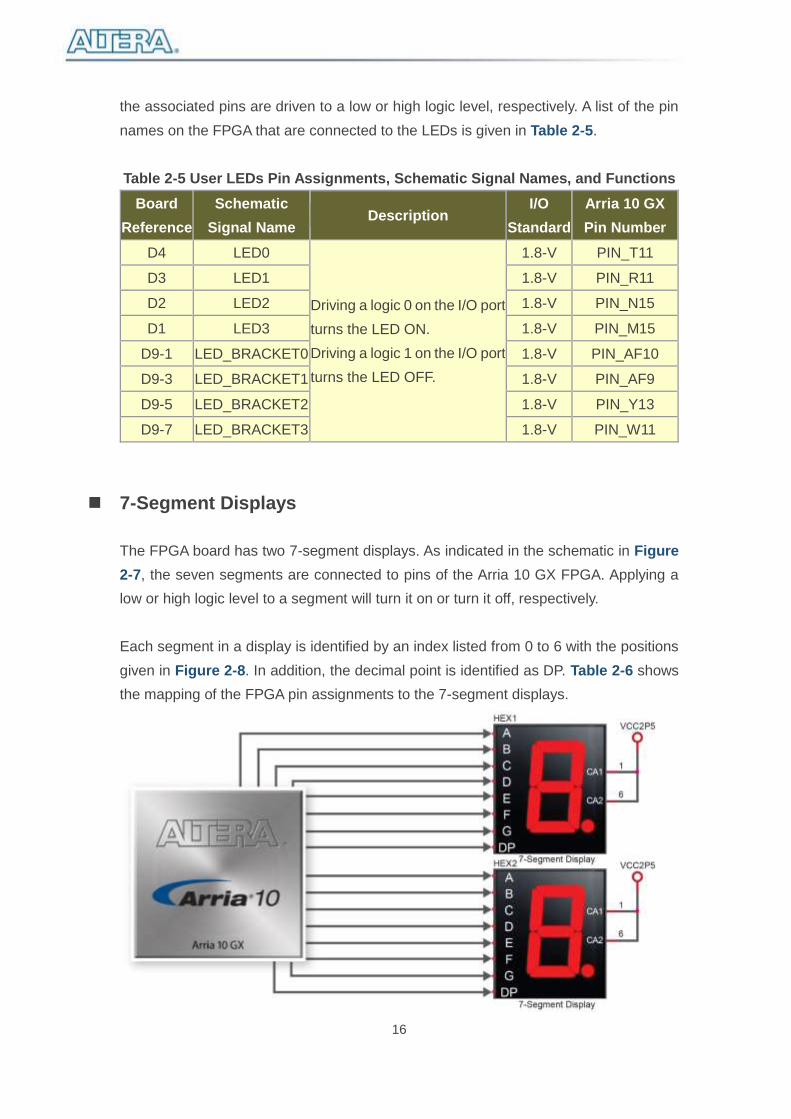
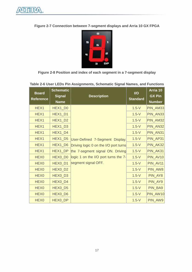
The FPGA board has two 7-segment displays. As indicated in the schematic in Figure
2-7, the seven segments are connected to pins of the Arria 10 GX FPGA. Applying a
low or high logic level to a segment will turn it on or turn it off, respectively.
Each segment in a display is identified by an index listed from 0 to 6 with the positions
given in Figure 2-8. In addition, the decimal point is identified as DP. Table 2-6 shows
the mapping of the FPGA pin assignments to the 7-segment displays.
17
Figure 2-7 Connection between 7-segment displays and Arria 10 GX FPGA
Figure 2-8 Position and index of each segment in a 7-segment display
Table 2-6 User LEDs Pin Assignments, Schematic Signal Names, and Functions
Board
Reference
Schematic
Signal
Name
Description I/O
Standard
Arria 10
GX Pin
Number
HEX1 HEX1_D0
User-Defined 7-Segment Display.
Driving logic 0 on the I/O port turns
the 7-segment signal ON. Driving
logic 1 on the I/O port turns the 7-
segment signal OFF.
1.5-V PIN_AM33
HEX1 HEX1_D1 1.5-V PIN_AN33
HEX1 HEX1_D2 1.5-V PIN_AM32
HEX1 HEX1_D3 1.5-V PIN_AN32
HEX1 HEX1_D4 1.5-V PIN_AN31
HEX1 HEX1_D5 1.5-V PIN_AP31
HEX1 HEX1_D6 1.5-V PIN_AK32
HEX1 HEX1_DP 1.5-V PIN_AK31
HEX0 HEX0_D0 1.5-V PIN_AV10
HEX0 HEX0_D1 1.5-V PIN_AV11
HEX0 HEX0_D2 1.5-V PIN_AW8
HEX0 HEX0_D3 1.5-V PIN_AY8
HEX0 HEX0_D4 1.5-V PIN_AY9
HEX0 HEX0_D5 1.5-V PIN_BA9
HEX0 HEX0_D6 1.5-V PIN_AW10
HEX0 HEX0_DP 1.5-V PIN_AW9
18
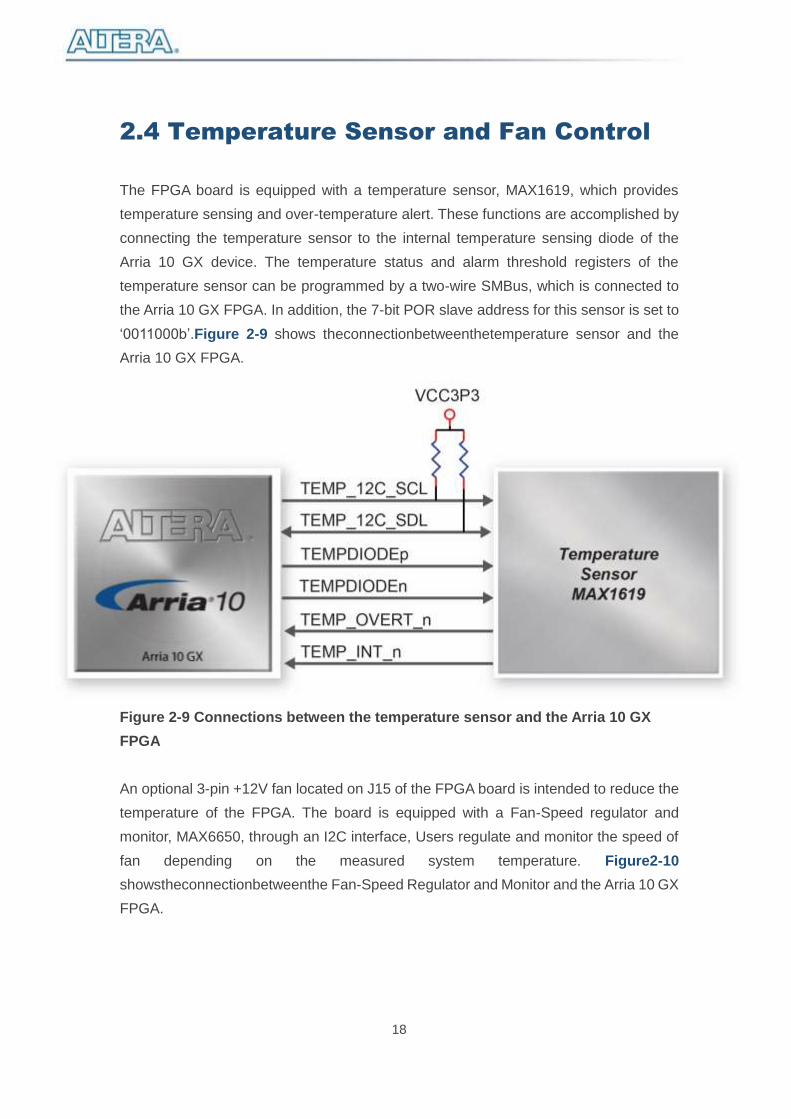
2.4 Temperature Sensor and Fan Control
The FPGA board is equipped with a temperature sensor, MAX1619, which provides
temperature sensing and over-temperature alert. These functions are accomplished by
connecting the temperature sensor to the internal temperature sensing diode of the
Arria 10 GX device. The temperature status and alarm threshold registers of the
temperature sensor can be programmed by a two-wire SMBus, which is connected to
the Arria 10 GX FPGA. In addition, the 7-bit POR slave address for this sensor is set to
‘0011000b’.Figure 2-9 shows theconnectionbetweenthetemperature sensor and the
Arria 10 GX FPGA.
Figure 2-9 Connections between the temperature sensor and the Arria 10 GX
FPGA
An optional 3-pin +12V fan located on J15 of the FPGA board is intended to reduce the
temperature of the FPGA. The board is equipped with a Fan-Speed regulator and
monitor, MAX6650, through an I2C interface, Users regulate and monitor the speed of
fan depending on the measured system temperature. Figure2-10
showstheconnectionbetweenthe Fan-Speed Regulator and Monitor and the Arria 10 GX
FPGA.
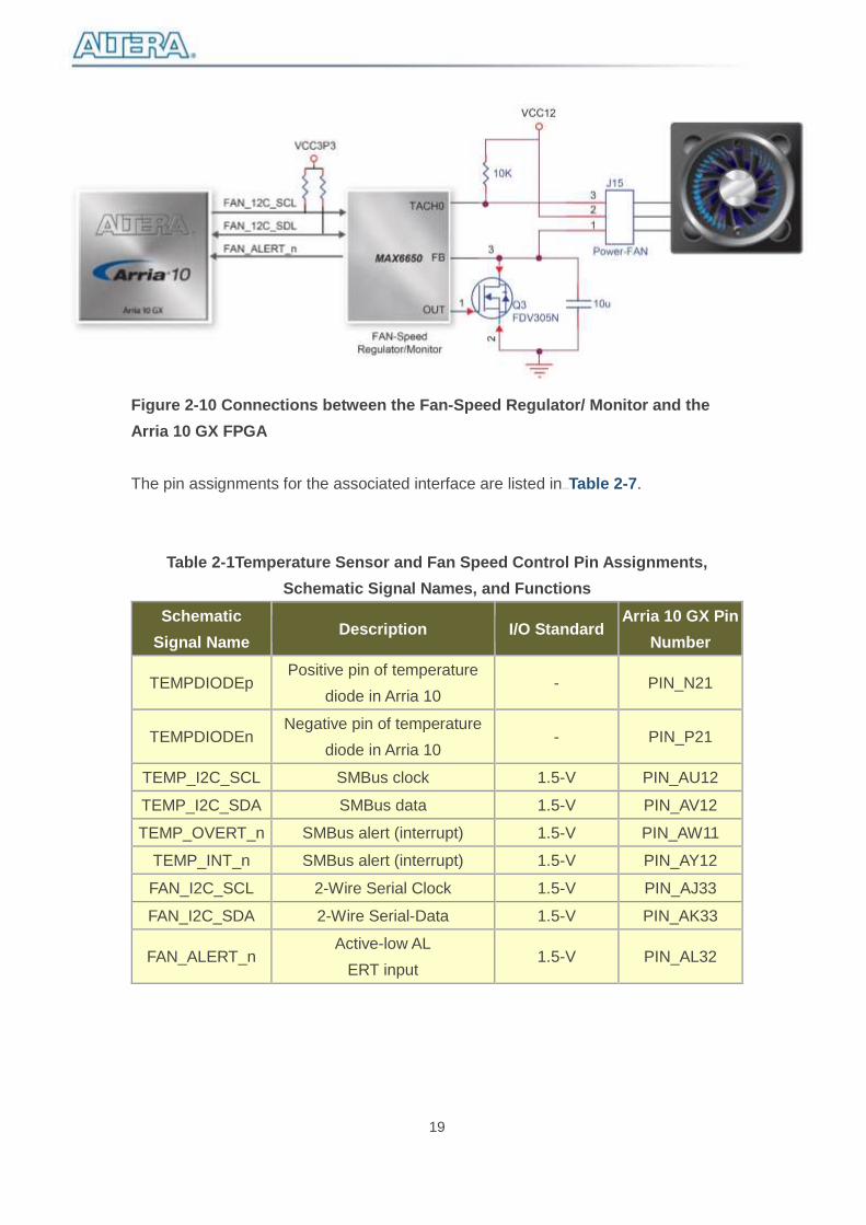
19
Figure 2-10 Connections between the Fan-Speed Regulator/ Monitor and the
Arria 10 GX FPGA
The pin assignments for the associated interface are listed in 109H109HTable 2-7.
Table 2-1Temperature Sensor and Fan Speed Control Pin Assignments,
Schematic Signal Names, and Functions
Schematic
Signal Name Description I/O Standard
Arria 10 GX Pin
Number
TEMPDIODEp Positive pin of temperature
diode in Arria 10 - PIN_N21
TEMPDIODEn Negative pin of temperature
diode in Arria 10 - PIN_P21
TEMP_I2C_SCL SMBus clock 1.5-V PIN_AU12
TEMP_I2C_SDA SMBus data 1.5-V PIN_AV12
TEMP_OVERT_n SMBus alert (interrupt) 1.5-V PIN_AW11
TEMP_INT_n SMBus alert (interrupt) 1.5-V PIN_AY12
FAN_I2C_SCL 2-Wire Serial Clock 1.5-V PIN_AJ33
FAN_I2C_SDA 2-Wire Serial-Data 1.5-V PIN_AK33
FAN_ALERT_n Active-low AL
ERT input 1.5-V PIN_AL32
20
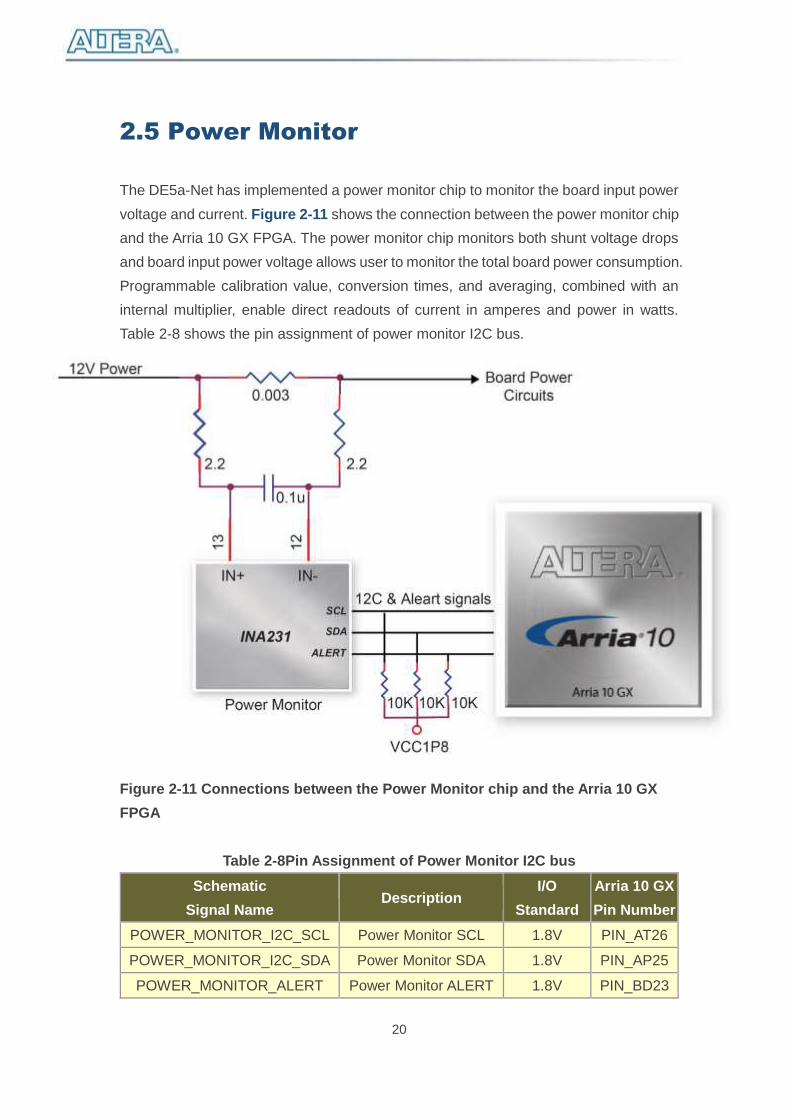
2.5 Power Monitor
The DE5a-Net has implemented a power monitor chip to monitor the board input power
voltage and current. Figure 2-11 shows the connection between the power monitor chip
and the Arria 10 GX FPGA. The power monitor chip monitors both shunt voltage drops
and board input power voltage allows user to monitor the total board power consumption.
Programmable calibration value, conversion times, and averaging, combined with an
internal multiplier, enable direct readouts of current in amperes and power in watts.
Table 2-8 shows the pin assignment of power monitor I2C bus.
Figure 2-11 Connections between the Power Monitor chip and the Arria 10 GX
FPGA
Table 2-8Pin Assignment of Power Monitor I2C bus
Schematic
Signal Name Description
I/O
Standard
Arria 10 GX
Pin Number
POWER_MONITOR_I2C_SCL Power Monitor SCL 1.8V PIN_AT26
POWER_MONITOR_I2C_SDA Power Monitor SDA 1.8V PIN_AP25
POWER_MONITOR_ALERT Power Monitor ALERT 1.8V PIN_BD23
21
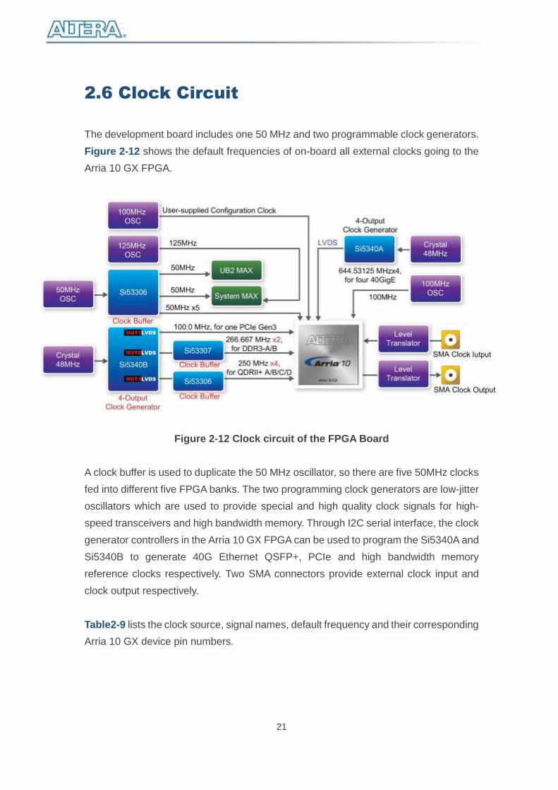
2.6 Clock Circuit
The development board includes one 50 MHz and two programmable clock generators.
Figure 2-12 shows the default frequencies of on-board all external clocks going to the
Arria 10 GX FPGA.
Figure 2-12 Clock circuit of the FPGA Board
A clock buffer is used to duplicate the 50 MHz oscillator, so there are five 50MHz clocks
fed into different five FPGA banks. The two programming clock generators are low-jitter
oscillators which are used to provide special and high quality clock signals for high-
speed transceivers and high bandwidth memory. Through I2C serial interface, the clock
generator controllers in the Arria 10 GX FPGA can be used to program the Si5340A and
Si5340B to generate 40G Ethernet QSFP+, PCIe and high bandwidth memory
reference clocks respectively. Two SMA connectors provide external clock input and
clock output respectively.
Table2-9 lists the clock source, signal names, default frequency and their corresponding
Arria 10 GX device pin numbers.
22
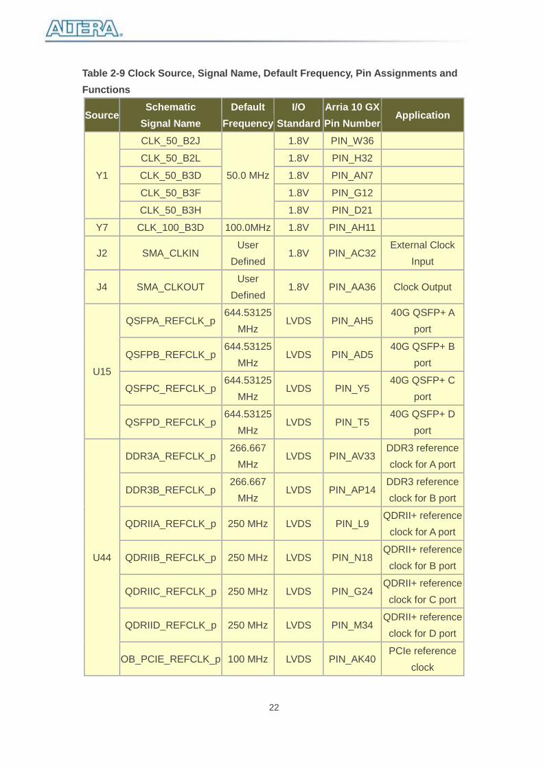
Table 2-9 Clock Source, Signal Name, Default Frequency, Pin Assignments and
Functions
Source Schematic
Signal Name
Default
Frequency
I/O
Standard
Arria 10 GX
Pin Number Application
Y1
CLK_50_B2J
50.0 MHz
1.8V PIN_W36
CLK_50_B2L 1.8V PIN_H32
CLK_50_B3D 1.8V PIN_AN7
CLK_50_B3F 1.8V PIN_G12
CLK_50_B3H 1.8V PIN_D21
Y7 CLK_100_B3D 100.0MHz 1.8V PIN_AH11
J2 SMA_CLKIN User
Defined 1.8V PIN_AC32
External Clock
Input
J4 SMA_CLKOUT User
Defined 1.8V PIN_AA36 Clock Output
U15
QSFPA_REFCLK_p 644.53125
MHz LVDS PIN_AH5
40G QSFP+ A
port
QSFPB_REFCLK_p 644.53125
MHz LVDS PIN_AD5
40G QSFP+ B
port
QSFPC_REFCLK_p 644.53125
MHz LVDS PIN_Y5
40G QSFP+ C
port
QSFPD_REFCLK_p 644.53125
MHz LVDS PIN_T5
40G QSFP+ D
port
U44
DDR3A_REFCLK_p 266.667
MHz LVDS PIN_AV33
DDR3 reference
clock for A port
DDR3B_REFCLK_p 266.667
MHz LVDS PIN_AP14
DDR3 reference
clock for B port
QDRIIA_REFCLK_p 250 MHz LVDS PIN_L9 QDRII+ reference
clock for A port
QDRIIB_REFCLK_p 250 MHz LVDS PIN_N18 QDRII+ reference
clock for B port
QDRIIC_REFCLK_p 250 MHz LVDS PIN_G24 QDRII+ reference
clock for C port
QDRIID_REFCLK_p 250 MHz LVDS PIN_M34 QDRII+ reference
clock for D port
OB_PCIE_REFCLK_p 100 MHz LVDS PIN_AK40 PCIe reference
clock
23
Table 2-10lists the programmable oscillator control pins, signal names, I/O standard
and their corresponding Arria 10 GX device pin numbers.
Table 2-10 Programmable oscillator control pin, Signal Name, I/O standard, Pin
Assignments and Descriptions
Programmable
Oscillator
Schematic
Signal Name
I/O
Standard
Arria 10 GX
Pin Number Description
Si5340A
(U15)
Si5340A_I2C_SCL 1.8-V PIN_AJ11 I2C bus, connected
with Si5340A Si5340A_I2C_SDA 1.8-V PIN_AN8
Si5340A
(U15)
Si5340A_RST 1.8-V PIN_AN6 Si5340A reset
signal
Si5340A_INTR 1.8-V PIN_AM6 Si5340A interrupt
signal
Si5340A_OE_n 1.8-V PIN_AJ10 Si5340A output
enable signal
Si5340B
(U44)
Si5340B_I2C_SCL 1.8-V PIN_G37 I2C bus, connected
with Si5340B Si5340B_I2C_SDA 1.8-V PIN_H31
Si5340B_RST 1.8-V PIN_G38 Si5340B reset
signal
Si5340B_INTR 1.8-V PIN_G32 Si5340B interrupt
signal
Si5340B_OE_n 1.5-V PIN_AL31 Si5340B output
enable signal
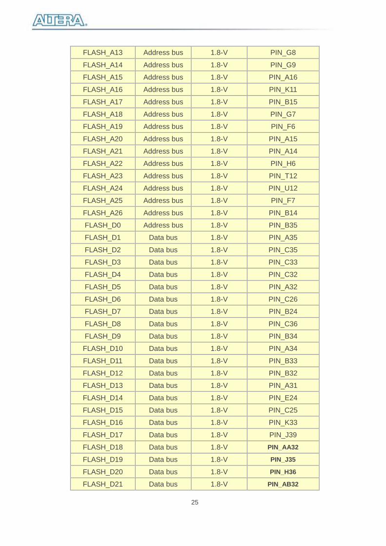
2.7 FLASH Memory
The development board has two 1Gb CFI-compatible synchronous flash devices for
non-volatile storage of FPGA configuration data, user application data, and user code
space.
Each interface has a 16-bit data bus and the two devices combined allow for FPP x32
configuration. This device is part of the shared flash and MAX (FM) bus, which connects
to the flash memory and MAX V CPLD (5M2210) System Controller. Figure 2-13 shows
the connections between the Flash, MAX and Arria 10 GX FPGA.

24
Figure 2-13 Connection between the Flash, Max and Arria 10 GX FPGA
Table 2-11lists the flash pin assignments, signal names, and functions.
Table 2-11 Flash Memory Pin Assignments, Schematic Signal Names, and
Functions
Schematic
Signal Name Description I/O Standard
Arria 10 GX Pin
Number
FLASH_A1 Address bus 1.8-V PIN_H26
FLASH_A2 Address bus 1.8-V PIN_J18
FLASH_A3 Address bus 1.8-V PIN_N17
FLASH_A4 Address bus 1.8-V PIN_P15
FLASH_A5 Address bus 1.8-V PIN_B18
FLASH_A6 Address bus 1.8-V PIN_E18
FLASH_A7 Address bus 1.8-V PIN_D18
FLASH_A8 Address bus 1.8-V PIN_J10
FLASH_A9 Address bus 1.8-V PIN_B17
FLASH_A10 Address bus 1.8-V PIN_J11
FLASH_A11 Address bus 1.8-V PIN_H8
FLASH_A12 Address bus 1.8-V PIN_A17
25
FLASH_A13 Address bus 1.8-V PIN_G8
FLASH_A14 Address bus 1.8-V PIN_G9
FLASH_A15 Address bus 1.8-V PIN_A16
FLASH_A16 Address bus 1.8-V PIN_K11
FLASH_A17 Address bus 1.8-V PIN_B15
FLASH_A18 Address bus 1.8-V PIN_G7
FLASH_A19 Address bus 1.8-V PIN_F6
FLASH_A20 Address bus 1.8-V PIN_A15
FLASH_A21 Address bus 1.8-V PIN_A14
FLASH_A22 Address bus 1.8-V PIN_H6
FLASH_A23 Address bus 1.8-V PIN_T12
FLASH_A24 Address bus 1.8-V PIN_U12
FLASH_A25 Address bus 1.8-V PIN_F7
FLASH_A26 Address bus 1.8-V PIN_B14
FLASH_D0 Address bus 1.8-V PIN_B35
FLASH_D1 Data bus 1.8-V PIN_A35
FLASH_D2 Data bus 1.8-V PIN_C35
FLASH_D3 Data bus 1.8-V PIN_C33
FLASH_D4 Data bus 1.8-V PIN_C32
FLASH_D5 Data bus 1.8-V PIN_A32
FLASH_D6 Data bus 1.8-V PIN_C26
FLASH_D7 Data bus 1.8-V PIN_B24
FLASH_D8 Data bus 1.8-V PIN_C36
FLASH_D9 Data bus 1.8-V PIN_B34
FLASH_D10 Data bus 1.8-V PIN_A34
FLASH_D11 Data bus 1.8-V PIN_B33
FLASH_D12 Data bus 1.8-V PIN_B32
FLASH_D13 Data bus 1.8-V PIN_A31
FLASH_D14 Data bus 1.8-V PIN_E24
FLASH_D15 Data bus 1.8-V PIN_C25
FLASH_D16 Data bus 1.8-V PIN_K33
FLASH_D17 Data bus 1.8-V PIN_J39
FLASH_D18 Data bus 1.8-V PIN_AA32
FLASH_D19 Data bus 1.8-V PIN_J35
FLASH_D20 Data bus 1.8-V PIN_H36
FLASH_D21 Data bus 1.8-V PIN_AB32
26
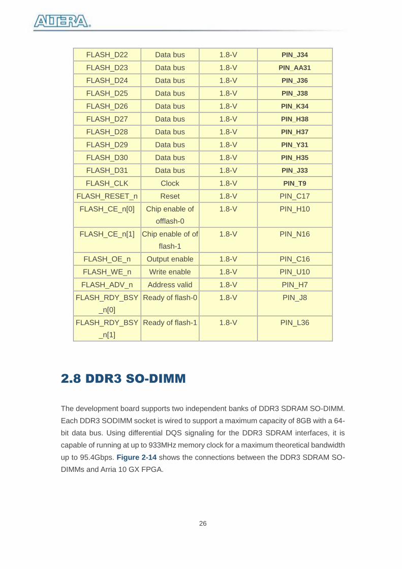
FLASH_D22 Data bus 1.8-V PIN_J34
FLASH_D23 Data bus 1.8-V PIN_AA31
FLASH_D24 Data bus 1.8-V PIN_J36
FLASH_D25 Data bus 1.8-V PIN_J38
FLASH_D26 Data bus 1.8-V PIN_K34
FLASH_D27 Data bus 1.8-V PIN_H38
FLASH_D28 Data bus 1.8-V PIN_H37
FLASH_D29 Data bus 1.8-V PIN_Y31
FLASH_D30 Data bus 1.8-V PIN_H35
FLASH_D31 Data bus 1.8-V PIN_J33
FLASH_CLK Clock 1.8-V PIN_T9
FLASH_RESET_n Reset 1.8-V PIN_C17
FLASH_CE_n[0] Chip enable of
offlash-0
1.8-V PIN_H10
FLASH_CE_n[1] Chip enable of of
flash-1
1.8-V PIN_N16
FLASH_OE_n Output enable 1.8-V PIN_C16
FLASH_WE_n Write enable 1.8-V PIN_U10
FLASH_ADV_n Address valid 1.8-V PIN_H7
FLASH_RDY_BSY
_n[0]
Ready of flash-0 1.8-V PIN_J8
FLASH_RDY_BSY
_n[1]
Ready of flash-1 1.8-V PIN_L36
2.8 DDR3 SO-DIMM
The development board supports two independent banks of DDR3 SDRAM SO-DIMM.
Each DDR3 SODIMM socket is wired to support a maximum capacity of 8GB with a 64-
bit data bus. Using differential DQS signaling for the DDR3 SDRAM interfaces, it is
capable of running at up to 933MHz memory clock for a maximum theoretical bandwidth
up to 95.4Gbps. Figure 2-14 shows the connections between the DDR3 SDRAM SO-
DIMMs and Arria 10 GX FPGA.
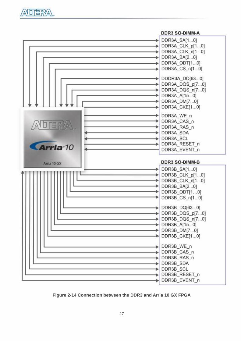
27
Figure 2-14 Connection between the DDR3 and Arria 10 GX FPGA
28
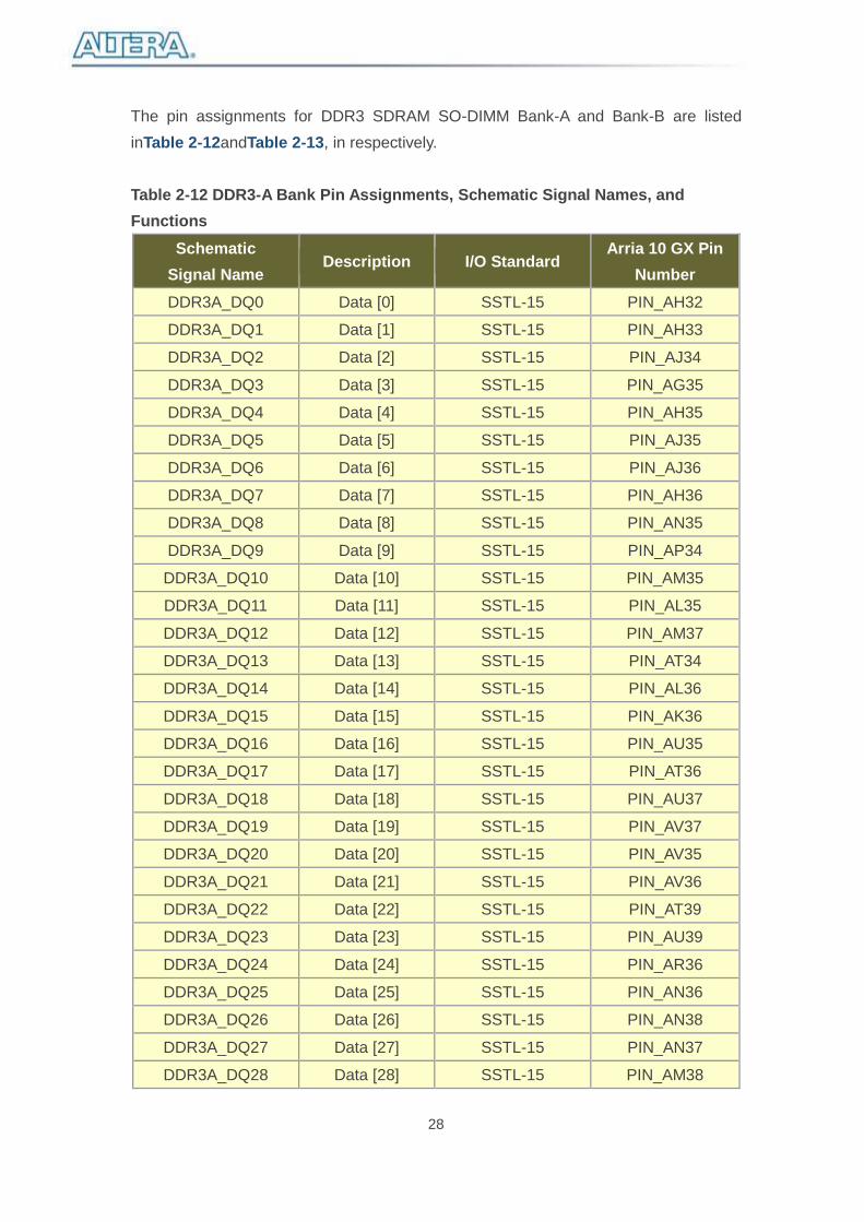
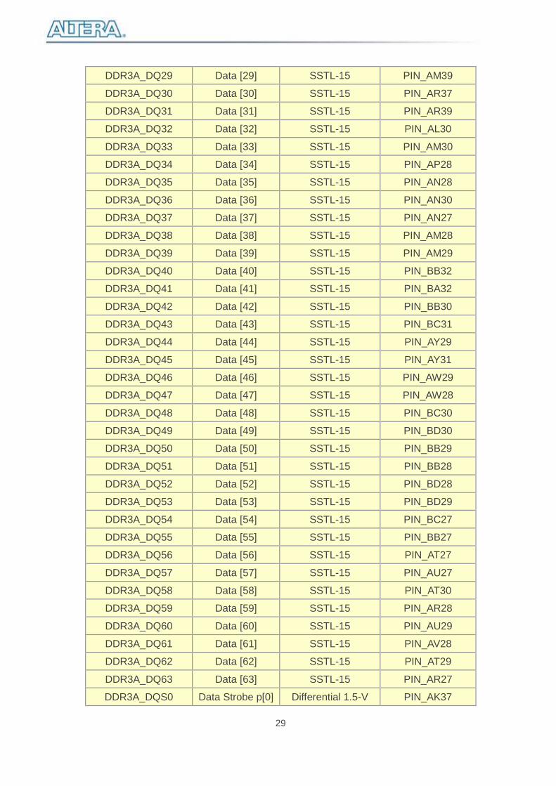
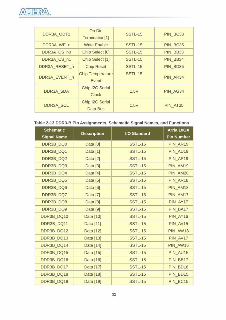
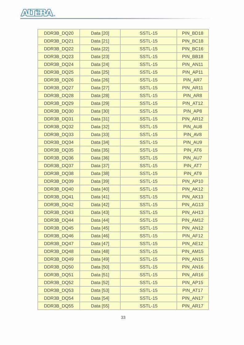
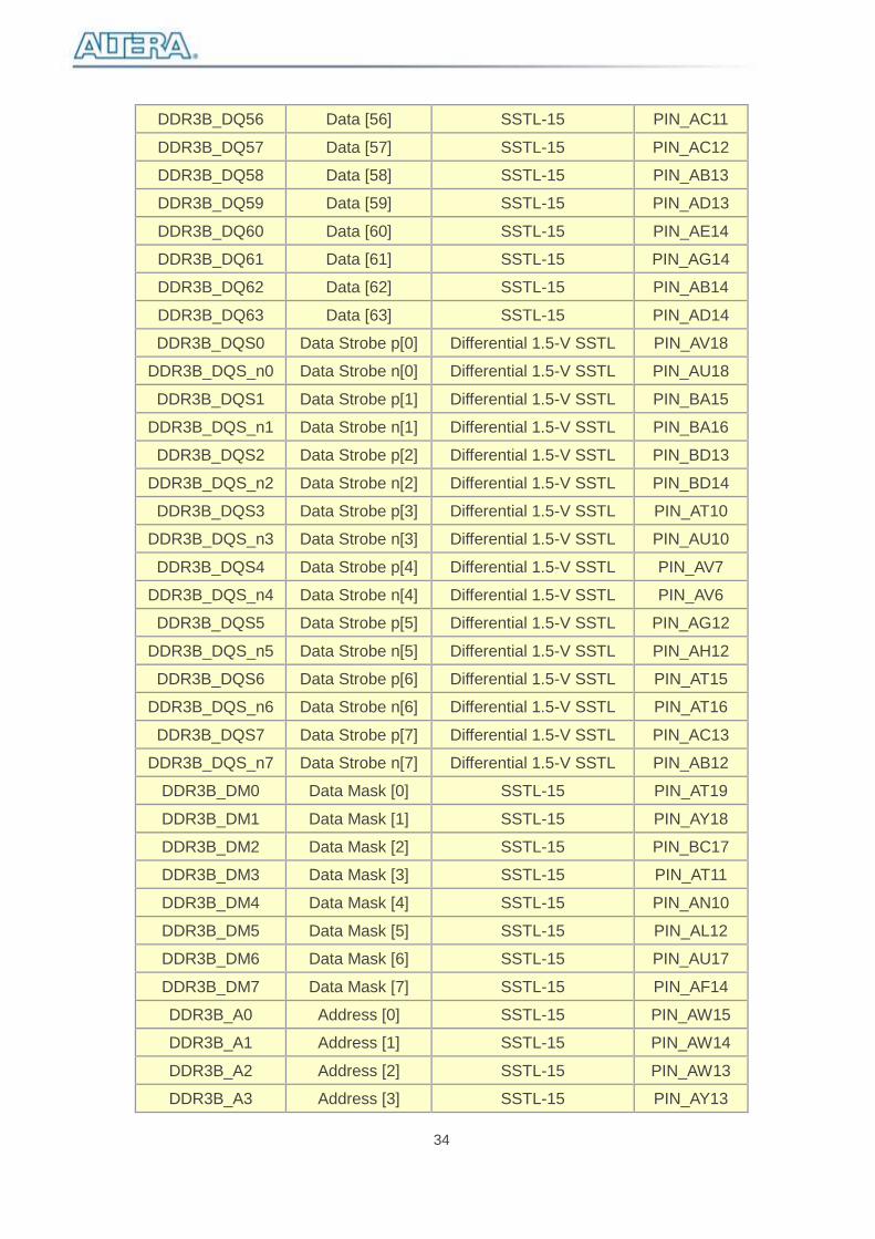
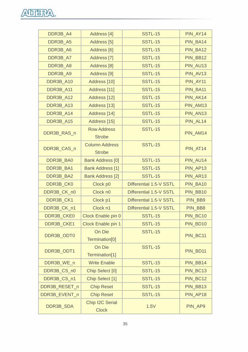
The pin assignments for DDR3 SDRAM SO-DIMM Bank-A and Bank-B are listed
inTable 2-12andTable 2-13, in respectively.
Table 2-12 DDR3-A Bank Pin Assignments, Schematic Signal Names, and
Functions
Schematic
Signal Name Description I/O Standard
Arria 10 GX Pin
Number
DDR3A_DQ0 Data [0] SSTL-15 PIN_AH32
DDR3A_DQ1 Data [1] SSTL-15 PIN_AH33
DDR3A_DQ2 Data [2] SSTL-15 PIN_AJ34
DDR3A_DQ3 Data [3] SSTL-15 PIN_AG35
DDR3A_DQ4 Data [4] SSTL-15 PIN_AH35
DDR3A_DQ5 Data [5] SSTL-15 PIN_AJ35
DDR3A_DQ6 Data [6] SSTL-15 PIN_AJ36
DDR3A_DQ7 Data [7] SSTL-15 PIN_AH36
DDR3A_DQ8 Data [8] SSTL-15 PIN_AN35
DDR3A_DQ9 Data [9] SSTL-15 PIN_AP34
DDR3A_DQ10 Data [10] SSTL-15 PIN_AM35
DDR3A_DQ11 Data [11] SSTL-15 PIN_AL35
DDR3A_DQ12 Data [12] SSTL-15 PIN_AM37
DDR3A_DQ13 Data [13] SSTL-15 PIN_AT34
DDR3A_DQ14 Data [14] SSTL-15 PIN_AL36
DDR3A_DQ15 Data [15] SSTL-15 PIN_AK36
DDR3A_DQ16 Data [16] SSTL-15 PIN_AU35
DDR3A_DQ17 Data [17] SSTL-15 PIN_AT36
DDR3A_DQ18 Data [18] SSTL-15 PIN_AU37
DDR3A_DQ19 Data [19] SSTL-15 PIN_AV37
DDR3A_DQ20 Data [20] SSTL-15 PIN_AV35
DDR3A_DQ21 Data [21] SSTL-15 PIN_AV36
DDR3A_DQ22 Data [22] SSTL-15 PIN_AT39
DDR3A_DQ23 Data [23] SSTL-15 PIN_AU39
DDR3A_DQ24 Data [24] SSTL-15 PIN_AR36
DDR3A_DQ25 Data [25] SSTL-15 PIN_AN36
DDR3A_DQ26 Data [26] SSTL-15 PIN_AN38
DDR3A_DQ27 Data [27] SSTL-15 PIN_AN37
DDR3A_DQ28 Data [28] SSTL-15 PIN_AM38
29
DDR3A_DQ29 Data [29] SSTL-15 PIN_AM39
DDR3A_DQ30 Data [30] SSTL-15 PIN_AR37
DDR3A_DQ31 Data [31] SSTL-15 PIN_AR39
DDR3A_DQ32 Data [32] SSTL-15 PIN_AL30
DDR3A_DQ33 Data [33] SSTL-15 PIN_AM30
DDR3A_DQ34 Data [34] SSTL-15 PIN_AP28
DDR3A_DQ35 Data [35] SSTL-15 PIN_AN28
DDR3A_DQ36 Data [36] SSTL-15 PIN_AN30
DDR3A_DQ37 Data [37] SSTL-15 PIN_AN27
DDR3A_DQ38 Data [38] SSTL-15 PIN_AM28
DDR3A_DQ39 Data [39] SSTL-15 PIN_AM29
DDR3A_DQ40 Data [40] SSTL-15 PIN_BB32
DDR3A_DQ41 Data [41] SSTL-15 PIN_BA32
DDR3A_DQ42 Data [42] SSTL-15 PIN_BB30
DDR3A_DQ43 Data [43] SSTL-15 PIN_BC31
DDR3A_DQ44 Data [44] SSTL-15 PIN_AY29
DDR3A_DQ45 Data [45] SSTL-15 PIN_AY31
DDR3A_DQ46 Data [46] SSTL-15 PIN_AW29
DDR3A_DQ47 Data [47] SSTL-15 PIN_AW28
DDR3A_DQ48 Data [48] SSTL-15 PIN_BC30
DDR3A_DQ49 Data [49] SSTL-15 PIN_BD30
DDR3A_DQ50 Data [50] SSTL-15 PIN_BB29
DDR3A_DQ51 Data [51] SSTL-15 PIN_BB28
DDR3A_DQ52 Data [52] SSTL-15 PIN_BD28
DDR3A_DQ53 Data [53] SSTL-15 PIN_BD29
DDR3A_DQ54 Data [54] SSTL-15 PIN_BC27
DDR3A_DQ55 Data [55] SSTL-15 PIN_BB27
DDR3A_DQ56 Data [56] SSTL-15 PIN_AT27
DDR3A_DQ57 Data [57] SSTL-15 PIN_AU27
DDR3A_DQ58 Data [58] SSTL-15 PIN_AT30
DDR3A_DQ59 Data [59] SSTL-15 PIN_AR28
DDR3A_DQ60 Data [60] SSTL-15 PIN_AU29
DDR3A_DQ61 Data [61] SSTL-15 PIN_AV28
DDR3A_DQ62 Data [62] SSTL-15 PIN_AT29
DDR3A_DQ63 Data [63] SSTL-15 PIN_AR27
DDR3A_DQS0 Data Strobe p[0] Differential 1.5-V PIN_AK37

30
SSTL
DDR3A_DQS_n0 Data Strobe n[0] Differential 1.5-V
SSTL PIN_AL37
DDR3A_DQS1 Data Strobe p[1] Differential 1.5-V
SSTL PIN_AL34
DDR3A_DQS_n1 Data Strobe n[1] Differential 1.5-V
SSTL PIN_AM34
DDR3A_DQS2 Data Strobe p[2] Differential 1.5-V
SSTL PIN_AU38
DDR3A_DQS_n2 Data Strobe n[2] Differential 1.5-V
SSTL PIN_AV38
DDR3A_DQS3 Data Strobe p[3] Differential 1.5-V
SSTL PIN_AP38
DDR3A_DQS_n3 Data Strobe n[4] Differential 1.5-V
SSTL PIN_AR38
DDR3A_DQS4 Data Strobe p[4] Differential 1.5-V
SSTL PIN_AP29
DDR3A_DQS_n4 Data Strobe n[4] Differential 1.5-V
SSTL PIN_AR29
DDR3A_DQS5 Data Strobe p[5] Differential 1.5-V
SSTL PIN_BA29
DDR3A_DQS_n5 Data Strobe n[5] Differential 1.5-V
SSTL PIN_BA30
DDR3A_DQS6 Data Strobe p[6] Differential 1.5-V
SSTL PIN_BA26
DDR3A_DQS_n6 Data Strobe n[6] Differential 1.5-V
SSTL PIN_BA27
DDR3A_DQS7 Data Strobe p[7] Differential 1.5-V
SSTL PIN_AV30
DDR3A_DQS_n7 Data Strobe n[7] Differential 1.5-V
SSTL PIN_AW30
DDR3A_DM0 Data Mask [0] SSTL-15 PIN_AK34
DDR3A_DM1 Data Mask [1] SSTL-15 PIN_AP35
DDR3A_DM2 Data Mask [2] SSTL-15 PIN_AT37
DDR3A_DM3 Data Mask [3] SSTL-15 PIN_AP36
DDR3A_DM4 Data Mask [4] SSTL-15 PIN_AP30
DDR3A_DM5 Data Mask [5] SSTL-15 PIN_BA31

31
DDR3A_DM6 Data Mask [6] SSTL-15 PIN_BD31
DDR3A_DM7 Data Mask [7] SSTL-15 PIN_AU30
DDR3A_A0 Address [0] SSTL-15 PIN_AW34
DDR3A_A1 Address [1] SSTL-15 PIN_AY34
DDR3A_A2 Address [2] SSTL-15 PIN_AV31
DDR3A_A3 Address [3] SSTL-15 PIN_AW31
DDR3A_A4 Address [4] SSTL-15 PIN_BA37
DDR3A_A5 Address [5] SSTL-15 PIN_BB37
DDR3A_A6 Address [6] SSTL-15 PIN_AY36
DDR3A_A7 Address [7] SSTL-15 PIN_AY37
DDR3A_A8 Address [8] SSTL-15 PIN_AY32
DDR3A_A9 Address [9] SSTL-15 PIN_AY33
DDR3A_A10 Address [10] SSTL-15 PIN_AW35
DDR3A_A11 Address [11] SSTL-15 PIN_AW36
DDR3A_A12 Address [12] SSTL-15 PIN_AU34
DDR3A_A13 Address [13] SSTL-15 PIN_AT31
DDR3A_A14 Address [14] SSTL-15 PIN_AT32
DDR3A_A15 Address [15] SSTL-15 PIN_AU32
DDR3A_RAS_n Row Address
Strobe
SSTL-15 PIN_AV32
DDR3A_CAS_n Column Address
Strobe
SSTL-15 PIN_AR31
DDR3A_BA0 Bank Address [0] SSTL-15 PIN_AR32
DDR3A_BA1 Bank Address [1] SSTL-15 PIN_AP33
DDR3A_BA2 Bank Address [2] SSTL-15 PIN_AR33
DDR3A_CK0 Clock p0 Differential 1.5-V
SSTL PIN_BA34
DDR3A_CK_n0 Clock n0 Differential 1.5-V
SSTL PIN_BB35
DDR3A_CK1 Clock p1 Differential 1.5-V
SSTL PIN_BA35
DDR3A_CK_n1 Clock n1 Differential 1.5-V
SSTL PIN_BA36
DDR3A_CKE0 Clock Enable pin 0 SSTL-15 PIN_BD33
DDR3A_CKE1 Clock Enable pin 1 SSTL-15 PIN_BD34
DDR3A_ODT0 On Die
Termination[0] SSTL-15 PIN_BC32
32
DDR3A_ODT1 On Die
Termination[1] SSTL-15 PIN_BC33
DDR3A_WE_n Write Enable SSTL-15 PIN_BC35
DDR3A_CS_n0 Chip Select [0] SSTL-15 PIN_BB33
DDR3A_CS_n1 Chip Select [1] SSTL-15 PIN_BB34
DDR3A_RESET_n Chip Reset SSTL-15 PIN_BD35
DDR3A_EVENT_n Chip Temperature
Event
SSTL-15 PIN_AR34
DDR3A_SDA Chip I2C Serial
Clock 1.5V PIN_AG34
DDR3A_SCL Chip I2C Serial
Data Bus 1.5V PIN_AT35
Table 2-13 DDR3-B Pin Assignments, Schematic Signal Names, and Functions
Schematic
Signal Name Description I/O Standard
Arria 10GX
Pin Number
DDR3B_DQ0 Data [0] SSTL-15 PIN_AR19
DDR3B_DQ1 Data [1] SSTL-15 PIN_AU19
DDR3B_DQ2 Data [2] SSTL-15 PIN_AP19
DDR3B_DQ3 Data [3] SSTL-15 PIN_AM19
DDR3B_DQ4 Data [4] SSTL-15 PIN_AM20
DDR3B_DQ5 Data [5] SSTL-15 PIN_AR18
DDR3B_DQ6 Data [6] SSTL-15 PIN_AM18
DDR3B_DQ7 Data [7] SSTL-15 PIN_AM17
DDR3B_DQ8 Data [8] SSTL-15 PIN_AY17
DDR3B_DQ9 Data [9] SSTL-15 PIN_BA17
DDR3B_DQ10 Data [10] SSTL-15 PIN_AY16
DDR3B_DQ11 Data [11] SSTL-15 PIN_AV15
DDR3B_DQ12 Data [12] SSTL-15 PIN_AW18
DDR3B_DQ13 Data [13] SSTL-15 PIN_AV17
DDR3B_DQ14 Data [14] SSTL-15 PIN_AW16
DDR3B_DQ15 Data [15] SSTL-15 PIN_AU15
DDR3B_DQ16 Data [16] SSTL-15 PIN_BB17
DDR3B_DQ17 Data [17] SSTL-15 PIN_BD16
DDR3B_DQ18 Data [18] SSTL-15 PIN_BD15
DDR3B_DQ19 Data [19] SSTL-15 PIN_BC15
33
DDR3B_DQ20 Data [20] SSTL-15 PIN_BD18
DDR3B_DQ21 Data [21] SSTL-15 PIN_BC18
DDR3B_DQ22 Data [22] SSTL-15 PIN_BC16
DDR3B_DQ23 Data [23] SSTL-15 PIN_BB18
DDR3B_DQ24 Data [24] SSTL-15 PIN_AN11
DDR3B_DQ25 Data [25] SSTL-15 PIN_AP11
DDR3B_DQ26 Data [26] SSTL-15 PIN_AR7
DDR3B_DQ27 Data [27] SSTL-15 PIN_AR11
DDR3B_DQ28 Data [28] SSTL-15 PIN_AR8
DDR3B_DQ29 Data [29] SSTL-15 PIN_AT12
DDR3B_DQ30 Data [30] SSTL-15 PIN_AP8
DDR3B_DQ31 Data [31] SSTL-15 PIN_AR12
DDR3B_DQ32 Data [32] SSTL-15 PIN_AU8
DDR3B_DQ33 Data [33] SSTL-15 PIN_AV8
DDR3B_DQ34 Data [34] SSTL-15 PIN_AU9
DDR3B_DQ35 Data [35] SSTL-15 PIN_AT6
DDR3B_DQ36 Data [36] SSTL-15 PIN_AU7
DDR3B_DQ37 Data [37] SSTL-15 PIN_AT7
DDR3B_DQ38 Data [38] SSTL-15 PIN_AT9
DDR3B_DQ39 Data [39] SSTL-15 PIN_AP10
DDR3B_DQ40 Data [40] SSTL-15 PIN_AK12
DDR3B_DQ41 Data [41] SSTL-15 PIN_AK13
DDR3B_DQ42 Data [42] SSTL-15 PIN_AG13
DDR3B_DQ43 Data [43] SSTL-15 PIN_AH13
DDR3B_DQ44 Data [44] SSTL-15 PIN_AM12
DDR3B_DQ45 Data [45] SSTL-15 PIN_AN12
DDR3B_DQ46 Data [46] SSTL-15 PIN_AF12
DDR3B_DQ47 Data [47] SSTL-15 PIN_AE12
DDR3B_DQ48 Data [48] SSTL-15 PIN_AM15
DDR3B_DQ49 Data [49] SSTL-15 PIN_AN15
DDR3B_DQ50 Data [50] SSTL-15 PIN_AN16
DDR3B_DQ51 Data [51] SSTL-15 PIN_AR16
DDR3B_DQ52 Data [52] SSTL-15 PIN_AP15
DDR3B_DQ53 Data [53] SSTL-15 PIN_AT17
DDR3B_DQ54 Data [54] SSTL-15 PIN_AN17
DDR3B_DQ55 Data [55] SSTL-15 PIN_AR17
34
DDR3B_DQ56 Data [56] SSTL-15 PIN_AC11
DDR3B_DQ57 Data [57] SSTL-15 PIN_AC12
DDR3B_DQ58 Data [58] SSTL-15 PIN_AB13
DDR3B_DQ59 Data [59] SSTL-15 PIN_AD13
DDR3B_DQ60 Data [60] SSTL-15 PIN_AE14
DDR3B_DQ61 Data [61] SSTL-15 PIN_AG14
DDR3B_DQ62 Data [62] SSTL-15 PIN_AB14
DDR3B_DQ63 Data [63] SSTL-15 PIN_AD14
DDR3B_DQS0 Data Strobe p[0] Differential 1.5-V SSTL PIN_AV18
DDR3B_DQS_n0 Data Strobe n[0] Differential 1.5-V SSTL PIN_AU18
DDR3B_DQS1 Data Strobe p[1] Differential 1.5-V SSTL PIN_BA15
DDR3B_DQS_n1 Data Strobe n[1] Differential 1.5-V SSTL PIN_BA16
DDR3B_DQS2 Data Strobe p[2] Differential 1.5-V SSTL PIN_BD13
DDR3B_DQS_n2 Data Strobe n[2] Differential 1.5-V SSTL PIN_BD14
DDR3B_DQS3 Data Strobe p[3] Differential 1.5-V SSTL PIN_AT10
DDR3B_DQS_n3 Data Strobe n[3] Differential 1.5-V SSTL PIN_AU10
DDR3B_DQS4 Data Strobe p[4] Differential 1.5-V SSTL PIN_AV7
DDR3B_DQS_n4 Data Strobe n[4] Differential 1.5-V SSTL PIN_AV6
DDR3B_DQS5 Data Strobe p[5] Differential 1.5-V SSTL PIN_AG12
DDR3B_DQS_n5 Data Strobe n[5] Differential 1.5-V SSTL PIN_AH12
DDR3B_DQS6 Data Strobe p[6] Differential 1.5-V SSTL PIN_AT15
DDR3B_DQS_n6 Data Strobe n[6] Differential 1.5-V SSTL PIN_AT16
DDR3B_DQS7 Data Strobe p[7] Differential 1.5-V SSTL PIN_AC13
DDR3B_DQS_n7 Data Strobe n[7] Differential 1.5-V SSTL PIN_AB12
DDR3B_DM0 Data Mask [0] SSTL-15 PIN_AT19
DDR3B_DM1 Data Mask [1] SSTL-15 PIN_AY18
DDR3B_DM2 Data Mask [2] SSTL-15 PIN_BC17
DDR3B_DM3 Data Mask [3] SSTL-15 PIN_AT11
DDR3B_DM4 Data Mask [4] SSTL-15 PIN_AN10
DDR3B_DM5 Data Mask [5] SSTL-15 PIN_AL12
DDR3B_DM6 Data Mask [6] SSTL-15 PIN_AU17
DDR3B_DM7 Data Mask [7] SSTL-15 PIN_AF14
DDR3B_A0 Address [0] SSTL-15 PIN_AW15
DDR3B_A1 Address [1] SSTL-15 PIN_AW14
DDR3B_A2 Address [2] SSTL-15 PIN_AW13
DDR3B_A3 Address [3] SSTL-15 PIN_AY13
35
DDR3B_A4 Address [4] SSTL-15 PIN_AY14
DDR3B_A5 Address [5] SSTL-15 PIN_BA14
DDR3B_A6 Address [6] SSTL-15 PIN_BA12
DDR3B_A7 Address [7] SSTL-15 PIN_BB12
DDR3B_A8 Address [8] SSTL-15 PIN_AU13
DDR3B_A9 Address [9] SSTL-15 PIN_AV13
DDR3B_A10 Address [10] SSTL-15 PIN_AY11
DDR3B_A11 Address [11] SSTL-15 PIN_BA11
DDR3B_A12 Address [12] SSTL-15 PIN_AK14
DDR3B_A13 Address [13] SSTL-15 PIN_AM13
DDR3B_A14 Address [14] SSTL-15 PIN_AN13
DDR3B_A15 Address [15] SSTL-15 PIN_AL14
DDR3B_RAS_n Row Address
Strobe
SSTL-15 PIN_AM14
DDR3B_CAS_n Column Address
Strobe
SSTL-15 PIN_AT14
DDR3B_BA0 Bank Address [0] SSTL-15 PIN_AU14
DDR3B_BA1 Bank Address [1] SSTL-15 PIN_AP13
DDR3B_BA2 Bank Address [2] SSTL-15 PIN_AR13
DDR3B_CK0 Clock p0 Differential 1.5-V SSTL PIN_BA10
DDR3B_CK_n0 Clock n0 Differential 1.5-V SSTL PIN_BB10
DDR3B_CK1 Clock p1 Differential 1.5-V SSTL PIN_BB9
DDR3B_CK_n1 Clock n1 Differential 1.5-V SSTL PIN_BB8
DDR3B_CKE0 Clock Enable pin 0 SSTL-15 PIN_BC10
DDR3B_CKE1 Clock Enable pin 1 SSTL-15 PIN_BD10
DDR3B_ODT0 On Die
Termination[0]
SSTL-15 PIN_BC11
DDR3B_ODT1 On Die
Termination[1]
SSTL-15 PIN_BD11
DDR3B_WE_n Write Enable SSTL-15 PIN_BB14
DDR3B_CS_n0 Chip Select [0] SSTL-15 PIN_BC13
DDR3B_CS_n1 Chip Select [1] SSTL-15 PIN_BC12
DDR3B_RESET_n Chip Reset SSTL-15 PIN_BB13
DDR3B_EVENT_n Chip Reset SSTL-15 PIN_AP18
DDR3B_SDA Chip I2C Serial
Clock 1.5V PIN_AP9
36
DDR3B_SCL Chip I2C Serial
Data Bus 1.5V PIN_AP16
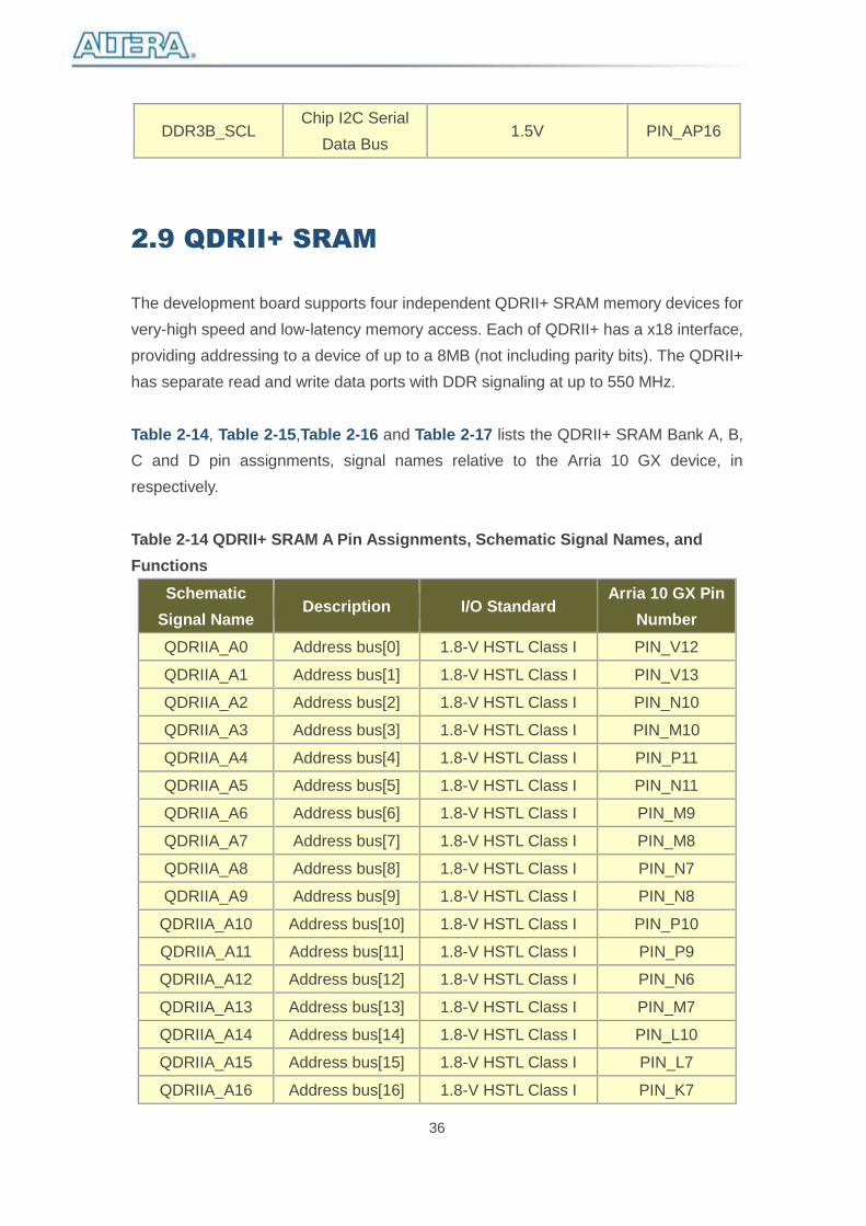
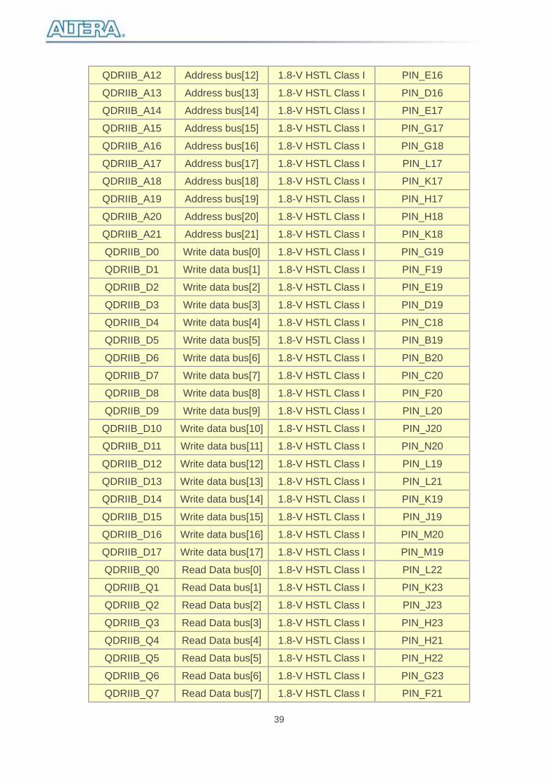
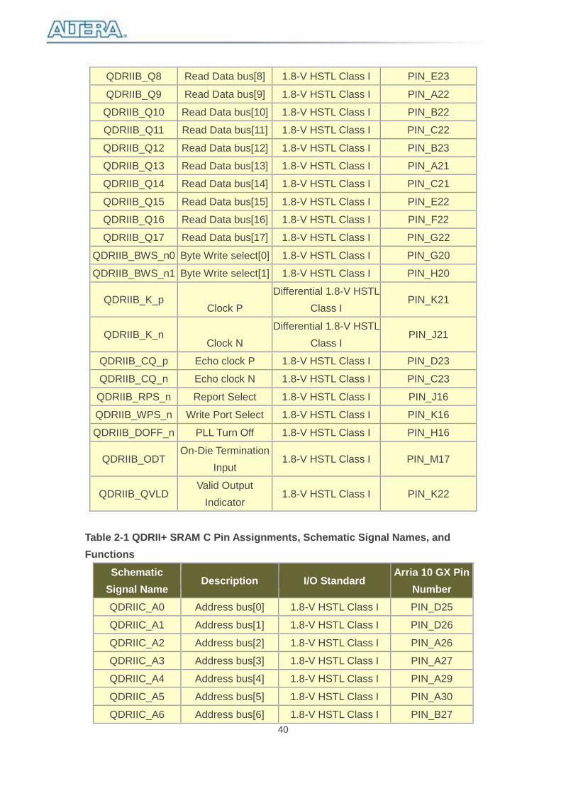
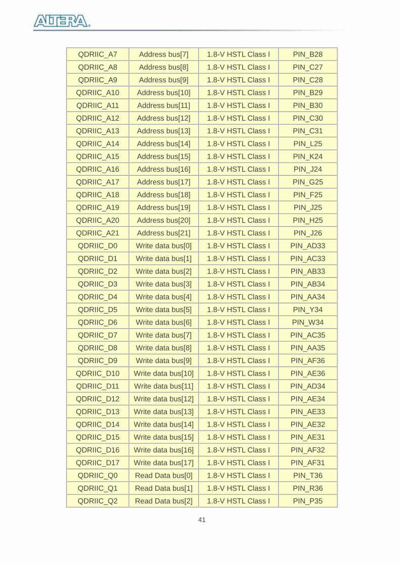
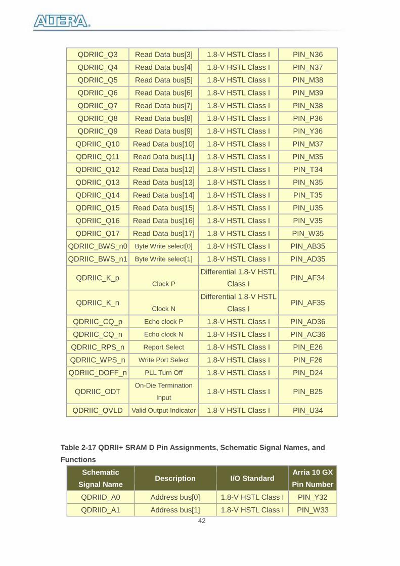
2.9 QDRII+ SRAM
The development board supports four independent QDRII+ SRAM memory devices for
very-high speed and low-latency memory access. Each of QDRII+ has a x18 interface,
providing addressing to a device of up to a 8MB (not including parity bits). The QDRII+
has separate read and write data ports with DDR signaling at up to 550 MHz.
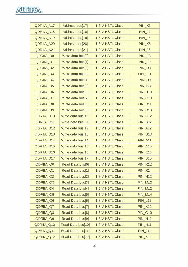
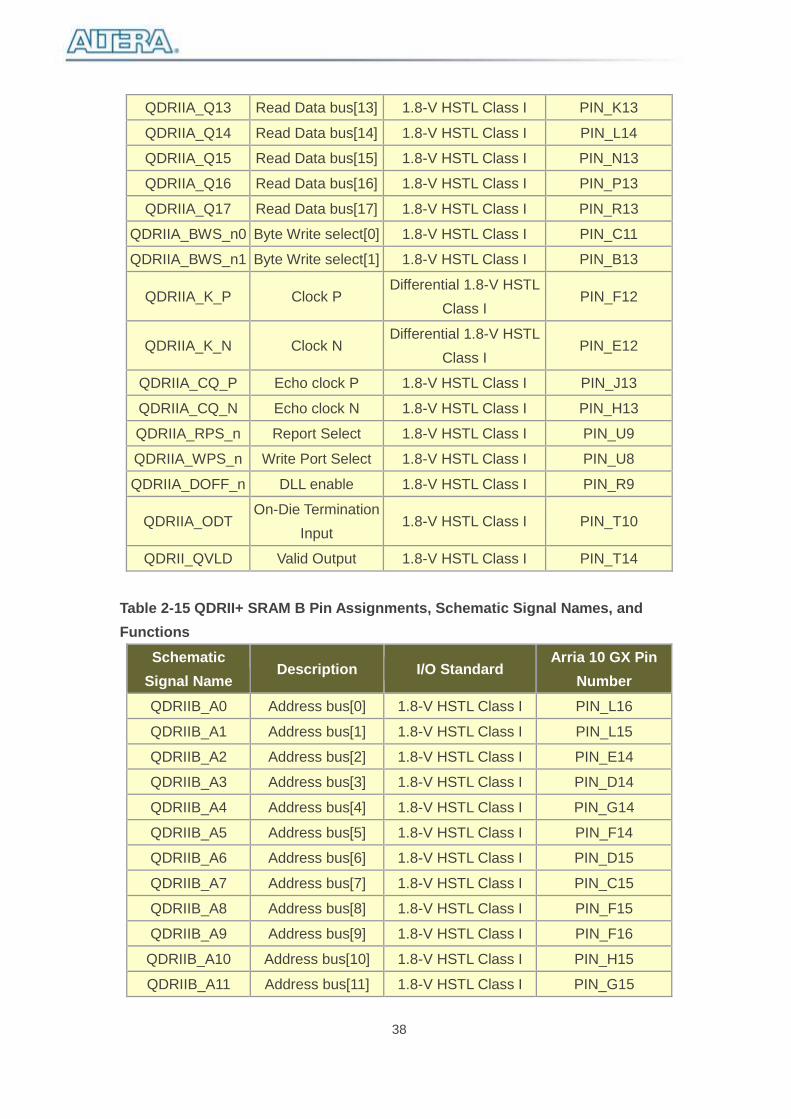
Table 2-14, Table 2-15,Table 2-16 and Table 2-17 lists the QDRII+ SRAM Bank A, B,
C and D pin assignments, signal names relative to the Arria 10 GX device, in
respectively.
Table 2-14 QDRII+ SRAM A Pin Assignments, Schematic Signal Names, and
Functions
Schematic
Signal Name Description I/O Standard
Arria 10 GX Pin
Number
QDRIIA_A0 Address bus[0] 1.8-V HSTL Class I PIN_V12
QDRIIA_A1 Address bus[1] 1.8-V HSTL Class I PIN_V13
QDRIIA_A2 Address bus[2] 1.8-V HSTL Class I PIN_N10
QDRIIA_A3 Address bus[3] 1.8-V HSTL Class I PIN_M10
QDRIIA_A4 Address bus[4] 1.8-V HSTL Class I PIN_P11
QDRIIA_A5 Address bus[5] 1.8-V HSTL Class I PIN_N11
QDRIIA_A6 Address bus[6] 1.8-V HSTL Class I PIN_M9
QDRIIA_A7 Address bus[7] 1.8-V HSTL Class I PIN_M8
QDRIIA_A8 Address bus[8] 1.8-V HSTL Class I PIN_N7
QDRIIA_A9 Address bus[9] 1.8-V HSTL Class I PIN_N8
QDRIIA_A10 Address bus[10] 1.8-V HSTL Class I PIN_P10
QDRIIA_A11 Address bus[11] 1.8-V HSTL Class I PIN_P9
QDRIIA_A12 Address bus[12] 1.8-V HSTL Class I PIN_N6
QDRIIA_A13 Address bus[13] 1.8-V HSTL Class I PIN_M7
QDRIIA_A14 Address bus[14] 1.8-V HSTL Class I PIN_L10
QDRIIA_A15 Address bus[15] 1.8-V HSTL Class I PIN_L7
QDRIIA_A16 Address bus[16] 1.8-V HSTL Class I PIN_K7
37
QDRIIA_A17 Address bus[17] 1.8-V HSTL Class I PIN_K8
QDRIIA_A18 Address bus[18] 1.8-V HSTL Class I PIN_J9
QDRIIA_A19 Address bus[19] 1.8-V HSTL Class I PIN_L6
QDRIIA_A20 Address bus[20] 1.8-V HSTL Class I PIN_K6
QDRIIA_A21 Address bus[21] 1.8-V HSTL Class I PIN_J6
QDRIIA_D0 Write data bus[0] 1.8-V HSTL Class I PIN_E8
QDRIIA_D1 Write data bus[1] 1.8-V HSTL Class I PIN_E9
QDRIIA_D2 Write data bus[2] 1.8-V HSTL Class I PIN_D8
QDRIIA_D3 Write data bus[3] 1.8-V HSTL Class I PIN_E11
QDRIIA_D4 Write data bus[4] 1.8-V HSTL Class I PIN_D9
QDRIIA_D5 Write data bus[5] 1.8-V HSTL Class I PIN_C8
QDRIIA_D6 Write data bus[6] 1.8-V HSTL Class I PIN_D10
QDRIIA_D7 Write data bus[7] 1.8-V HSTL Class I PIN_C10
QDRIIA_D8 Write data bus[8] 1.8-V HSTL Class I PIN_D11
QDRIIA_D9 Write data bus[9] 1.8-V HSTL Class I PIN_C13
QDRIIA_D10 Write data bus[10] 1.8-V HSTL Class I PIN_C12
QDRIIA_D11 Write data bus[11] 1.8-V HSTL Class I PIN_B12
QDRIIA_D12 Write data bus[12] 1.8-V HSTL Class I PIN_A12
QDRIIA_D13 Write data bus[13] 1.8-V HSTL Class I PIN_D13
QDRIIA_D14 Write data bus[14] 1.8-V HSTL Class I PIN_A11
QDRIIA_D15 Write data bus[15] 1.8-V HSTL Class I PIN_A10
QDRIIA_D16 Write data bus[16] 1.8-V HSTL Class I PIN_E13
QDRIIA_D17 Write data bus[17] 1.8-V HSTL Class I PIN_B10
QDRIIA_Q0 Read Data bus[0] 1.8-V HSTL Class I PIN_R12
QDRIIA_Q1 Read Data bus[1] 1.8-V HSTL Class I PIN_R14
QDRIIA_Q2 Read Data bus[2] 1.8-V HSTL Class I PIN_N12
QDRIIA_Q3 Read Data bus[3] 1.8-V HSTL Class I PIN_M13
QDRIIA_Q4 Read Data bus[4] 1.8-V HSTL Class I PIN_M12
QDRIIA_Q5 Read Data bus[5] 1.8-V HSTL Class I PIN_M14
QDRIIA_Q6 Read Data bus[6] 1.8-V HSTL Class I PIN_L12
QDRIIA_Q7 Read Data bus[7] 1.8-V HSTL Class I PIN_K12
QDRIIA_Q8 Read Data bus[8] 1.8-V HSTL Class I PIN_G10
QDRIIA_Q9 Read Data bus[9] 1.8-V HSTL Class I PIN_H12
QDRIIA_Q10 Read Data bus[10] 1.8-V HSTL Class I PIN_H11
QDRIIA_Q11 Read Data bus[11] 1.8-V HSTL Class I PIN_J14
QDRIIA_Q12 Read Data bus[12] 1.8-V HSTL Class I PIN_K14
38
QDRIIA_Q13 Read Data bus[13] 1.8-V HSTL Class I PIN_K13
QDRIIA_Q14 Read Data bus[14] 1.8-V HSTL Class I PIN_L14
QDRIIA_Q15 Read Data bus[15] 1.8-V HSTL Class I PIN_N13
QDRIIA_Q16 Read Data bus[16] 1.8-V HSTL Class I PIN_P13
QDRIIA_Q17 Read Data bus[17] 1.8-V HSTL Class I PIN_R13
QDRIIA_BWS_n0 Byte Write select[0] 1.8-V HSTL Class I PIN_C11
QDRIIA_BWS_n1 Byte Write select[1] 1.8-V HSTL Class I PIN_B13
QDRIIA_K_P Clock P Differential 1.8-V HSTL
Class I PIN_F12
QDRIIA_K_N Clock N Differential 1.8-V HSTL
Class I PIN_E12
QDRIIA_CQ_P Echo clock P 1.8-V HSTL Class I PIN_J13
QDRIIA_CQ_N Echo clock N 1.8-V HSTL Class I PIN_H13
QDRIIA_RPS_n Report Select 1.8-V HSTL Class I PIN_U9
QDRIIA_WPS_n Write Port Select 1.8-V HSTL Class I PIN_U8
QDRIIA_DOFF_n DLL enable 1.8-V HSTL Class I PIN_R9
QDRIIA_ODT On-Die Termination
Input 1.8-V HSTL Class I PIN_T10
QDRII_QVLD Valid Output 1.8-V HSTL Class I PIN_T14
Table 2-15 QDRII+ SRAM B Pin Assignments, Schematic Signal Names, and
Functions
Schematic
Signal Name Description I/O Standard
Arria 10 GX Pin
Number
QDRIIB_A0 Address bus[0] 1.8-V HSTL Class I PIN_L16
QDRIIB_A1 Address bus[1] 1.8-V HSTL Class I PIN_L15
QDRIIB_A2 Address bus[2] 1.8-V HSTL Class I PIN_E14
QDRIIB_A3 Address bus[3] 1.8-V HSTL Class I PIN_D14
QDRIIB_A4 Address bus[4] 1.8-V HSTL Class I PIN_G14
QDRIIB_A5 Address bus[5] 1.8-V HSTL Class I PIN_F14
QDRIIB_A6 Address bus[6] 1.8-V HSTL Class I PIN_D15
QDRIIB_A7 Address bus[7] 1.8-V HSTL Class I PIN_C15
QDRIIB_A8 Address bus[8] 1.8-V HSTL Class I PIN_F15
QDRIIB_A9 Address bus[9] 1.8-V HSTL Class I PIN_F16
QDRIIB_A10 Address bus[10] 1.8-V HSTL Class I PIN_H15
QDRIIB_A11 Address bus[11] 1.8-V HSTL Class I PIN_G15
39
QDRIIB_A12 Address bus[12] 1.8-V HSTL Class I PIN_E16
QDRIIB_A13 Address bus[13] 1.8-V HSTL Class I PIN_D16
QDRIIB_A14 Address bus[14] 1.8-V HSTL Class I PIN_E17
QDRIIB_A15 Address bus[15] 1.8-V HSTL Class I PIN_G17
QDRIIB_A16 Address bus[16] 1.8-V HSTL Class I PIN_G18
QDRIIB_A17 Address bus[17] 1.8-V HSTL Class I PIN_L17
QDRIIB_A18 Address bus[18] 1.8-V HSTL Class I PIN_K17
QDRIIB_A19 Address bus[19] 1.8-V HSTL Class I PIN_H17
QDRIIB_A20 Address bus[20] 1.8-V HSTL Class I PIN_H18
QDRIIB_A21 Address bus[21] 1.8-V HSTL Class I PIN_K18
QDRIIB_D0 Write data bus[0] 1.8-V HSTL Class I PIN_G19
QDRIIB_D1 Write data bus[1] 1.8-V HSTL Class I PIN_F19
QDRIIB_D2 Write data bus[2] 1.8-V HSTL Class I PIN_E19
QDRIIB_D3 Write data bus[3] 1.8-V HSTL Class I PIN_D19
QDRIIB_D4 Write data bus[4] 1.8-V HSTL Class I PIN_C18
QDRIIB_D5 Write data bus[5] 1.8-V HSTL Class I PIN_B19
QDRIIB_D6 Write data bus[6] 1.8-V HSTL Class I PIN_B20
QDRIIB_D7 Write data bus[7] 1.8-V HSTL Class I PIN_C20
QDRIIB_D8 Write data bus[8] 1.8-V HSTL Class I PIN_F20
QDRIIB_D9 Write data bus[9] 1.8-V HSTL Class I PIN_L20
QDRIIB_D10 Write data bus[10] 1.8-V HSTL Class I PIN_J20
QDRIIB_D11 Write data bus[11] 1.8-V HSTL Class I PIN_N20
QDRIIB_D12 Write data bus[12] 1.8-V HSTL Class I PIN_L19
QDRIIB_D13 Write data bus[13] 1.8-V HSTL Class I PIN_L21
QDRIIB_D14 Write data bus[14] 1.8-V HSTL Class I PIN_K19
QDRIIB_D15 Write data bus[15] 1.8-V HSTL Class I PIN_J19
QDRIIB_D16 Write data bus[16] 1.8-V HSTL Class I PIN_M20
QDRIIB_D17 Write data bus[17] 1.8-V HSTL Class I PIN_M19
QDRIIB_Q0 Read Data bus[0] 1.8-V HSTL Class I PIN_L22
QDRIIB_Q1 Read Data bus[1] 1.8-V HSTL Class I PIN_K23
QDRIIB_Q2 Read Data bus[2] 1.8-V HSTL Class I PIN_J23
QDRIIB_Q3 Read Data bus[3] 1.8-V HSTL Class I PIN_H23
QDRIIB_Q4 Read Data bus[4] 1.8-V HSTL Class I PIN_H21
QDRIIB_Q5 Read Data bus[5] 1.8-V HSTL Class I PIN_H22
QDRIIB_Q6 Read Data bus[6] 1.8-V HSTL Class I PIN_G23
QDRIIB_Q7 Read Data bus[7] 1.8-V HSTL Class I PIN_F21
40
QDRIIB_Q8 Read Data bus[8] 1.8-V HSTL Class I PIN_E23
QDRIIB_Q9 Read Data bus[9] 1.8-V HSTL Class I PIN_A22
QDRIIB_Q10 Read Data bus[10] 1.8-V HSTL Class I PIN_B22
QDRIIB_Q11 Read Data bus[11] 1.8-V HSTL Class I PIN_C22
QDRIIB_Q12 Read Data bus[12] 1.8-V HSTL Class I PIN_B23
QDRIIB_Q13 Read Data bus[13] 1.8-V HSTL Class I PIN_A21
QDRIIB_Q14 Read Data bus[14] 1.8-V HSTL Class I PIN_C21
QDRIIB_Q15 Read Data bus[15] 1.8-V HSTL Class I PIN_E22
QDRIIB_Q16 Read Data bus[16] 1.8-V HSTL Class I PIN_F22
QDRIIB_Q17 Read Data bus[17] 1.8-V HSTL Class I PIN_G22
QDRIIB_BWS_n0 Byte Write select[0] 1.8-V HSTL Class I PIN_G20
QDRIIB_BWS_n1 Byte Write select[1] 1.8-V HSTL Class I PIN_H20
QDRIIB_K_p Clock P
Differential 1.8-V HSTL
Class I PIN_K21
QDRIIB_K_n Clock N
Differential 1.8-V HSTL
Class I PIN_J21
QDRIIB_CQ_p Echo clock P 1.8-V HSTL Class I PIN_D23
QDRIIB_CQ_n Echo clock N 1.8-V HSTL Class I PIN_C23
QDRIIB_RPS_n Report Select 1.8-V HSTL Class I PIN_J16
QDRIIB_WPS_n Write Port Select 1.8-V HSTL Class I PIN_K16
QDRIIB_DOFF_n PLL Turn Off 1.8-V HSTL Class I PIN_H16
QDRIIB_ODT On-Die Termination
Input 1.8-V HSTL Class I PIN_M17
QDRIIB_QVLD Valid Output
Indicator 1.8-V HSTL Class I PIN_K22
Table 2-1 QDRII+ SRAM C Pin Assignments, Schematic Signal Names, and
Functions
Schematic
Signal Name Description I/O Standard
Arria 10 GX Pin
Number
QDRIIC_A0 Address bus[0] 1.8-V HSTL Class I PIN_D25
QDRIIC_A1 Address bus[1] 1.8-V HSTL Class I PIN_D26
QDRIIC_A2 Address bus[2] 1.8-V HSTL Class I PIN_A26
QDRIIC_A3 Address bus[3] 1.8-V HSTL Class I PIN_A27
QDRIIC_A4 Address bus[4] 1.8-V HSTL Class I PIN_A29
QDRIIC_A5 Address bus[5] 1.8-V HSTL Class I PIN_A30
QDRIIC_A6 Address bus[6] 1.8-V HSTL Class I PIN_B27
41
QDRIIC_A7 Address bus[7] 1.8-V HSTL Class I PIN_B28
QDRIIC_A8 Address bus[8] 1.8-V HSTL Class I PIN_C27
QDRIIC_A9 Address bus[9] 1.8-V HSTL Class I PIN_C28
QDRIIC_A10 Address bus[10] 1.8-V HSTL Class I PIN_B29
QDRIIC_A11 Address bus[11] 1.8-V HSTL Class I PIN_B30
QDRIIC_A12 Address bus[12] 1.8-V HSTL Class I PIN_C30
QDRIIC_A13 Address bus[13] 1.8-V HSTL Class I PIN_C31
QDRIIC_A14 Address bus[14] 1.8-V HSTL Class I PIN_L25
QDRIIC_A15 Address bus[15] 1.8-V HSTL Class I PIN_K24
QDRIIC_A16 Address bus[16] 1.8-V HSTL Class I PIN_J24
QDRIIC_A17 Address bus[17] 1.8-V HSTL Class I PIN_G25
QDRIIC_A18 Address bus[18] 1.8-V HSTL Class I PIN_F25
QDRIIC_A19 Address bus[19] 1.8-V HSTL Class I PIN_J25
QDRIIC_A20 Address bus[20] 1.8-V HSTL Class I PIN_H25
QDRIIC_A21 Address bus[21] 1.8-V HSTL Class I PIN_J26
QDRIIC_D0 Write data bus[0] 1.8-V HSTL Class I PIN_AD33
QDRIIC_D1 Write data bus[1] 1.8-V HSTL Class I PIN_AC33
QDRIIC_D2 Write data bus[2] 1.8-V HSTL Class I PIN_AB33
QDRIIC_D3 Write data bus[3] 1.8-V HSTL Class I PIN_AB34
QDRIIC_D4 Write data bus[4] 1.8-V HSTL Class I PIN_AA34
QDRIIC_D5 Write data bus[5] 1.8-V HSTL Class I PIN_Y34
QDRIIC_D6 Write data bus[6] 1.8-V HSTL Class I PIN_W34
QDRIIC_D7 Write data bus[7] 1.8-V HSTL Class I PIN_AC35
QDRIIC_D8 Write data bus[8] 1.8-V HSTL Class I PIN_AA35
QDRIIC_D9 Write data bus[9] 1.8-V HSTL Class I PIN_AF36
QDRIIC_D10 Write data bus[10] 1.8-V HSTL Class I PIN_AE36
QDRIIC_D11 Write data bus[11] 1.8-V HSTL Class I PIN_AD34
QDRIIC_D12 Write data bus[12] 1.8-V HSTL Class I PIN_AE34
QDRIIC_D13 Write data bus[13] 1.8-V HSTL Class I PIN_AE33
QDRIIC_D14 Write data bus[14] 1.8-V HSTL Class I PIN_AE32
QDRIIC_D15 Write data bus[15] 1.8-V HSTL Class I PIN_AE31
QDRIIC_D16 Write data bus[16] 1.8-V HSTL Class I PIN_AF32
QDRIIC_D17 Write data bus[17] 1.8-V HSTL Class I PIN_AF31
QDRIIC_Q0 Read Data bus[0] 1.8-V HSTL Class I PIN_T36
QDRIIC_Q1 Read Data bus[1] 1.8-V HSTL Class I PIN_R36
QDRIIC_Q2 Read Data bus[2] 1.8-V HSTL Class I PIN_P35
42
QDRIIC_Q3 Read Data bus[3] 1.8-V HSTL Class I PIN_N36
QDRIIC_Q4 Read Data bus[4] 1.8-V HSTL Class I PIN_N37
QDRIIC_Q5 Read Data bus[5] 1.8-V HSTL Class I PIN_M38
QDRIIC_Q6 Read Data bus[6] 1.8-V HSTL Class I PIN_M39
QDRIIC_Q7 Read Data bus[7] 1.8-V HSTL Class I PIN_N38
QDRIIC_Q8 Read Data bus[8] 1.8-V HSTL Class I PIN_P36
QDRIIC_Q9 Read Data bus[9] 1.8-V HSTL Class I PIN_Y36
QDRIIC_Q10 Read Data bus[10] 1.8-V HSTL Class I PIN_M37
QDRIIC_Q11 Read Data bus[11] 1.8-V HSTL Class I PIN_M35
QDRIIC_Q12 Read Data bus[12] 1.8-V HSTL Class I PIN_T34
QDRIIC_Q13 Read Data bus[13] 1.8-V HSTL Class I PIN_N35
QDRIIC_Q14 Read Data bus[14] 1.8-V HSTL Class I PIN_T35
QDRIIC_Q15 Read Data bus[15] 1.8-V HSTL Class I PIN_U35
QDRIIC_Q16 Read Data bus[16] 1.8-V HSTL Class I PIN_V35
QDRIIC_Q17 Read Data bus[17] 1.8-V HSTL Class I PIN_W35
QDRIIC_BWS_n0 Byte Write select[0] 1.8-V HSTL Class I PIN_AB35
QDRIIC_BWS_n1 Byte Write select[1] 1.8-V HSTL Class I PIN_AD35
QDRIIC_K_p Clock P
Differential 1.8-V HSTL
Class I PIN_AF34
QDRIIC_K_n Clock N
Differential 1.8-V HSTL
Class I PIN_AF35
QDRIIC_CQ_p Echo clock P 1.8-V HSTL Class I PIN_AD36
QDRIIC_CQ_n Echo clock N 1.8-V HSTL Class I PIN_AC36
QDRIIC_RPS_n Report Select 1.8-V HSTL Class I PIN_E26
QDRIIC_WPS_n Write Port Select 1.8-V HSTL Class I PIN_F26
QDRIIC_DOFF_n PLL Turn Off 1.8-V HSTL Class I PIN_D24
QDRIIC_ODT On-Die Termination
Input 1.8-V HSTL Class I PIN_B25
QDRIIC_QVLD Valid Output Indicator 1.8-V HSTL Class I PIN_U34
Table 2-17 QDRII+ SRAM D Pin Assignments, Schematic Signal Names, and
Functions
Schematic
Signal Name Description I/O Standard
Arria 10 GX
Pin Number
QDRIID_A0 Address bus[0] 1.8-V HSTL Class I PIN_Y32
QDRIID_A1 Address bus[1] 1.8-V HSTL Class I PIN_W33
43
QDRIID_A2 Address bus[2] 1.8-V HSTL Class I PIN_P34
QDRIID_A3 Address bus[3] 1.8-V HSTL Class I PIN_P33
QDRIID_A4 Address bus[4] 1.8-V HSTL Class I PIN_L32
QDRIID_A5 Address bus[5] 1.8-V HSTL Class I PIN_K32
QDRIID_A6 Address bus[6] 1.8-V HSTL Class I PIN_R34
QDRIID_A7 Address bus[7] 1.8-V HSTL Class I PIN_R33
QDRIID_A8 Address bus[8] 1.8-V HSTL Class I PIN_T32
QDRIID_A9 Address bus[9] 1.8-V HSTL Class I PIN_R32
QDRIID_A10 Address bus[10] 1.8-V HSTL Class I PIN_N32
QDRIID_A11 Address bus[11] 1.8-V HSTL Class I PIN_M32
QDRIID_A12 Address bus[12] 1.8-V HSTL Class I PIN_T31
QDRIID_A13 Address bus[13] 1.8-V HSTL Class I PIN_R31
QDRIID_A14 Address bus[14] 1.8-V HSTL Class I PIN_K38
QDRIID_A15 Address bus[15] 1.8-V HSTL Class I PIN_L37
QDRIID_A16 Address bus[16] 1.8-V HSTL Class I PIN_K36
QDRIID_A17 Address bus[17] 1.8-V HSTL Class I PIN_N33
QDRIID_A18 Address bus[18] 1.8-V HSTL Class I PIN_M33
QDRIID_A19 Address bus[19] 1.8-V HSTL Class I PIN_L39
QDRIID_A20 Address bus[20] 1.8-V HSTL Class I PIN_K39
QDRIID_A21 Address bus[21] 1.8-V HSTL Class I PIN_L35
QDRIID_D0 Write data bus[0] 1.8-V HSTL Class I PIN_E36
QDRIID_D1 Write data bus[1] 1.8-V HSTL Class I PIN_F34
QDRIID_D2 Write data bus[2] 1.8-V HSTL Class I PIN_F39
QDRIID_D3 Write data bus[3] 1.8-V HSTL Class I PIN_F36
QDRIID_D4 Write data bus[4] 1.8-V HSTL Class I PIN_D33
QDRIID_D5 Write data bus[5] 1.8-V HSTL Class I PIN_F31
QDRIID_D6 Write data bus[6] 1.8-V HSTL Class I PIN_G30
QDRIID_D7 Write data bus[7] 1.8-V HSTL Class I PIN_H30
QDRIID_D8 Write data bus[8] 1.8-V HSTL Class I PIN_G29
QDRIID_D9 Write data bus[9] 1.8-V HSTL Class I PIN_E33
QDRIID_D10 Write data bus[10] 1.8-V HSTL Class I PIN_G39
QDRIID_D11 Write data bus[11] 1.8-V HSTL Class I PIN_E37
QDRIID_D12 Write data bus[12] 1.8-V HSTL Class I PIN_F37
QDRIID_D13 Write data bus[13] 1.8-V HSTL Class I PIN_E34
QDRIID_D14 Write data bus[14] 1.8-V HSTL Class I PIN_D36
QDRIID_D15 Write data bus[15] 1.8-V HSTL Class I PIN_C37
44
QDRIID_D16 Write data bus[16] 1.8-V HSTL Class I PIN_D35
QDRIID_D17 Write data bus[17] 1.8-V HSTL Class I PIN_D34
QDRIID_Q0 Read Data bus[0] 1.8-V HSTL Class I PIN_L29
QDRIID_Q1 Read Data bus[1] 1.8-V HSTL Class I PIN_N30
QDRIID_Q2 Read Data bus[2] 1.8-V HSTL Class I PIN_K29
QDRIID_Q3 Read Data bus[3] 1.8-V HSTL Class I PIN_J29
QDRIID_Q4 Read Data bus[4] 1.8-V HSTL Class I PIN_M30
QDRIID_Q5 Read Data bus[5] 1.8-V HSTL Class I PIN_J30
QDRIID_Q6 Read Data bus[6] 1.8-V HSTL Class I PIN_N31
QDRIID_Q7 Read Data bus[7] 1.8-V HSTL Class I PIN_P31
QDRIID_Q8 Read Data bus[8] 1.8-V HSTL Class I PIN_H33
QDRIID_Q9 Read Data bus[9] 1.8-V HSTL Class I PIN_G34
QDRIID_Q10 Read Data bus[10] 1.8-V HSTL Class I PIN_G33
QDRIID_Q11 Read Data bus[11] 1.8-V HSTL Class I PIN_L31
QDRIID_Q12 Read Data bus[12] 1.8-V HSTL Class I PIN_J31
QDRIID_Q13 Read Data bus[13] 1.8-V HSTL Class I PIN_K31
QDRIID_Q14 Read Data bus[14] 1.8-V HSTL Class I PIN_L30
QDRIID_Q15 Read Data bus[15] 1.8-V HSTL Class I PIN_M29
QDRIID_Q16 Read Data bus[16] 1.8-V HSTL Class I PIN_M28
QDRIID_Q17 Read Data bus[17] 1.8-V HSTL Class I PIN_N28
QDRIID_BWS_n0 Byte Write select[0] 1.8-V HSTL Class I PIN_F30
QDRIID_BWS_n1 Byte Write select[1] 1.8-V HSTL Class I PIN_E31
QDRIID_K_p Clock P Differential 1.8-V
HSTL Class I PIN_F32
QDRIID_K_n Clock N Differential 1.8-V
HSTL Class I PIN_E32
QDRIID_CQ_p Echo clock P 1.8-V HSTL Class I PIN_G35
QDRIID_CQ_n Echo clock N 1.8-V HSTL Class I PIN_F35
QDRIID_RPS_n Report Select 1.8-V HSTL Class I PIN_V33
QDRIID_WPS_n Write Port Select 1.8-V HSTL Class I PIN_V32
QDRIID_DOFF_n PLL Turn Off 1.8-V HSTL Class I PIN_W31
QDRIID_ODT On-Die Termination Input 1.8-V HSTL Class I PIN_Y33
QDRIID_QVLD ValidOutput Indicator 1.8-V HSTL Class I PIN_P28
45
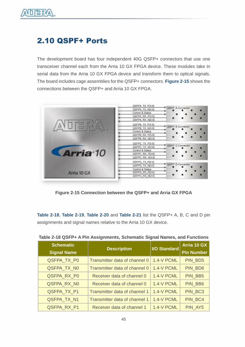
2.10 QSPF+ Ports
The development board has four independent 40G QSFP+ connectors that use one
transceiver channel each from the Arria 10 GX FPGA device. These modules take in
serial data from the Arria 10 GX FPGA device and transform them to optical signals.
The board includes cage assemblies for the QSFP+ connectors. Figure 2-15 shows the
connections between the QSFP+ and Arria 10 GX FPGA.
Figure 2-15 Connection between the QSFP+ and Arria GX FPGA
Table 2-18, Table 2-19, Table 2-20 and Table 2-21 list the QSFP+ A, B, C and D pin
assignments and signal names relative to the Arria 10 GX device.
Table 2-18 QSFP+ A Pin Assignments, Schematic Signal Names, and Functions
Schematic
Signal Name Description I/O Standard
Arria 10 GX
Pin Number
QSFPA_TX_P0 Transmitter data of channel 0 1.4-V PCML PIN_BD5
QSFPA_TX_N0 Transmitter data of channel 0 1.4-V PCML PIN_BD6
QSFPA_RX_P0 Receiver data of channel 0 1.4-V PCML PIN_BB5
QSFPA_RX_N0 Receiver data of channel 0 1.4-V PCML PIN_BB6
QSFPA_TX_P1 Transmitter data of channel 1 1.4-V PCML PIN_BC3
QSFPA_TX_N1 Transmitter data of channel 1 1.4-V PCML PIN_BC4
QSFPA_RX_P1 Receiver data of channel 1 1.4-V PCML PIN_AY5
46
QSFPA_RX_N1 Receiver data of channel 1 1.4-V PCML PIN_AY6
QSFPA_TX_P2 Transmitter data of channel 2 1.4-V PCML PIN_BB1
QSFPA_TX_N2 Transmitter data of channel 2 1.4-V PCML PIN_BB2
QSFPA_RX_P2 Receiver data of channel 2 1.4-V PCML PIN_BA3
QSFPA_RX_N2 Receiver data of channel 2 1.4-V PCML PIN_BA4
QSFPA_TX_P3 Transmitter data of channel 3 1.4-V PCML PIN_AY1
QSFPA_TX_N3 Transmitter data of channel 3 1.4-V PCML PIN_AY2
QSFPA_RX_P3 Receiver data of channel 3 1.4-V PCML PIN_AW3
QSFPA_RX_N3 Receiver data of channel 3 1.4-V PCML PIN_AW4
QSFPA_MOD_SEL_n Module Select 1.8V PIN_AC10
QSFPA_RST_n Module Reset 1.8V PIN_AA9
QSFPA_SCL 2-wire serial interface clock 1.8V PIN_AA10
QSFPA_SDA 2-wire serial interface data 1.8V PIN_Y9
QSFPA_LP_MODE Low Power Mode 1.8V PIN_AB10
QSFPA_INTERRUPT_n Interrupt 1.8V PIN_AB9
QSFPA_MOD_PRS_n Module Present 1.8V PIN_AG10
Table 2-19 QSFP+ B Pin Assignments, Schematic Signal Names, and Functions
Schematic
Signal Name Description I/O Standard
Arria 10 GX
Pin Number
QSFPB_TX_P0 Transmitter data of channel 0 1.4-V PCML PIN_AP1
QSFPB_TX_N0 Transmitter data of channel 0 1.4-V PCML PIN_AP2
QSFPB_RX_P0 Receiver data of channel 0 1.4-V PCML PIN_AN3
QSFPB_RX_N0 Receiver data of channel 0 1.4-V PCML PIN_AN4
QSFPB_TX_P1 Transmitter data of channel 1 1.4-V PCML PIN_AM1
QSFPB_TX_N1 Transmitter data of channel 1 1.4-V PCML PIN_AM2
QSFPB_RX_P1 Receiver data of channel 1 1.4-V PCML PIN_AL3
QSFPB_RX_N1 Receiver data of channel 1 1.4-V PCML PIN_AL4
QSFPB_TX_P2 Transmitter data of channel 2 1.4-V PCML PIN_AK1
QSFPB_TX_N2 Transmitter data of channel 2 1.4-V PCML PIN_AK2
QSFPB_RX_P2 Receiver data of channel 2 1.4-V PCML PIN_AJ3
QSFPB_RX_N2 Receiver data of channel 2 1.4-V PCML PIN_AJ4
QSFPB_TX_P3 Transmitter data of channel 3 1.4-V PCML PIN_AH1
QSFPB_TX_N3 Transmitter data of channel 3 1.4-V PCML PIN_AH2
QSFPB_RX_P3 Receiver data of channel 3 1.4-V PCML PIN_AG3
QSFPB_RX_N3 Receiver data of channel 3 1.4-V PCML PIN_AG4
47
QSFPB_MOD_SEL_n Module Select 1.8V PIN_AP6
QSFPB_RST_n Module Reset 1.8V PIN_AR6
QSFPB_SCL 2-wire serial interface clock 1.8V PIN_AM7
QSFPB_SDA 2-wire serial interface data 1.8V PIN_AM8
QSFPB_LP_MODE Low Power Mode 1.8V PIN_AM10
QSFPB_INTERRUPT_n Interrupt 1.8V PIN_AK9
QSFPB_MOD_PRS_n Module Present 1.8V PIN_AL10
Table 2-20 QSFP+ C Pin Assignments, Schematic Signal Names, and Functions
Schematic
Signal Name Description I/O Standard
Arria 10
GX Pin
Number
QSFPC_TX_P0 Transmitter data of channel 0 1.4-V PCML PIN_AB1
QSFPC_TX_N0 Transmitter data of channel 0 1.4-V PCML PIN_AB2
QSFPC_RX_P0 Receiver data of channel 0 1.4-V PCML PIN_AA3
QSFPC_RX_N0 Receiver data of channel 0 1.4-V PCML PIN_AA4
QSFPC_TX_P1 Transmitter data of channel 1 1.4-V PCML PIN_Y1
QSFPC_TX_N1 Transmitter data of channel 1 1.4-V PCML PIN_Y2
QSFPC_RX_P1 Receiver data of channel 1 1.4-V PCML PIN_W3
QSFPC_RX_N1 Receiver data of channel 1 1.4-V PCML PIN_W4
QSFPC_TX_P2 Transmitter data of channel 2 1.4-V PCML PIN_V1
QSFPC_TX_N2 Transmitter data of channel 2 1.4-V PCML PIN_V2
QSFPC_RX_P2 Receiver data of channel 2 1.4-V PCML PIN_U3
QSFPC_RX_N2 Receiver data of channel 2 1.4-V PCML PIN_U4
QSFPC_TX_P3 Transmitter data of channel 3 1.4-V PCML PIN_T1
QSFPC_TX_N3 Transmitter data of channel 3 1.4-V PCML PIN_T2
QSFPC_RX_P3 Receiver data of channel 3 1.4-V PCML PIN_R3
QSFPC_RX_N3 Receiver data of channel 3 1.4-V PCML PIN_R4
QSFPC_MOD_SEL_n Module Select 1.8V PIN_AL9
QSFPC_RST_n Module Reset 1.8V PIN_AJ9
QSFPC_SCL 2-wire serial interface clock 1.8V PIN_AL11
QSFPC_SDA 2-wire serial interface data 1.8V PIN_AK11
QSFPC_LP_MODE Low Power Mode 1.8V PIN_AH10
48
QSFPC_INTERRUPT_n Interrupt 1.8V PIN_AD11
QSFPC_MOD_PRS_n Module Present 1.8V PIN_AD10
Table 2-21 QSFP+ D Pin Assignments, Schematic Signal Names, and Functions
Schematic
Signal Name Description I/O Standard
Arria 10
GX Pin
Number
QSFPD_TX_P0 Transmitter data of channel 0 1.4-V PCML PIN_K1
QSFPD_TX_N0 Transmitter data of channel 0 1.4-V PCML PIN_K2
QSFPD_RX_P0 Receiver data of channel 0 1.4-V PCML PIN_J3
QSFPD_RX_N0 Receiver data of channel 0 1.4-V PCML PIN_J4
QSFPD_TX_P1 Transmitter data of channel 1 1.4-V PCML PIN_H1
QSFPD_TX_N1 Transmitter data of channel 1 1.4-V PCML PIN_H2
QSFPD_RX_P1 Receiver data of channel 1 1.4-V PCML PIN_G3
QSFPD_RX_N1 Receiver data of channel 1 1.4-V PCML PIN_G4
QSFPD_TX_P2 Transmitter data of channel 2 1.4-V PCML PIN_F1
QSFPD_TX_N2 Transmitter data of channel 2 1.4-V PCML PIN_F2
QSFPD_RX_P2 Receiver data of channel 2 1.4-V PCML PIN_E3
QSFPD_RX_N2 Receiver data of channel 2 1.4-V PCML PIN_E4
QSFPD_TX_P3 Transmitter data of channel 3 1.4-V PCML PIN_D1
QSFPD_TX_N3 Transmitter data of channel 3 1.4-V PCML PIN_D2
QSFPD_RX_P3 Receiver data of channel 3 1.4-V PCML PIN_D5
QSFPD_RX_N3 Receiver data of channel 3 1.4-V PCML PIN_D6
QSFPD_MOD_SEL_n Module Select 1.8V PIN_AA11
QSFPD_RST_n Module Reset 1.8V PIN_Y11
QSFPD_SCL 2-wire serial interface clock 1.8V PIN_W9
QSFPD_SDA 2-wire serial interface data 1.8V PIN_W10
QSFPD_LP_MODE Low Power Mode 1.8V PIN_AA12
QSFPD_INTERRUPT_n Interrupt 1.8V PIN_W13
QSFPD_MOD_PRS_n Module Present 1.8V PIN_Y12
2.11 PCI Express
The FPGA development board is designed to fit entirely into a PC motherboard with x8
or x16 PCI Express slot. Utilizing built-in transceivers on a Arria 10 GX device, it is able
to provide a fully integrated PCI Express-compliant solution for multi-lane (x1, x4, and
49
x8) applications. With the PCI Express hard IP block incorporated in the Arria 10 GX
device, it will allow users to implement simple and fast protocol, as well as saving logic
resources for logic application. Figure 2-16 presents the pin connection established
between the Arria 10 GX and PCI Express.
The PCI Express interface supports complete PCI Express Gen1 at 2.5Gbps/lane,
Gen2 at 5.0Gbps/lane, and Gen3 at 8.0Gbps/lane protocol stack solution compliant to
PCI Express base specification 3.0 that includes PHY-MAC, Data Link, and transaction
layer circuitry embedded in PCI Express hard IP blocks.
Please note that it is a requirement that you connect the PCIe external power connector
to 6-pin 12V DC power connector in the FPGA to avoid FPGA damage due to insufficient
power. The PCIE_REFCLK_p signal is a differential input that is driven from the PC
motherboard on this board through the PCIe edge connector. A DIP switch (SW5) is
connected to the PCI Express to allow different configurations to enable a x1, x4, or x8
PCIe.
Table 2-22 summarizes the PCI Express pin assignments of the signal names relative
to the Arria 10 GX FPGA.
Figure 2-16 PCI Express pin connection
Table 2-22 PCI Express Pin Assignments, Schematic Signal Names, and
Functions
Schematic
Signal Name Description I/O Standard
Arria 10 GX
Pin Number
50
PCIE_TX_p0 Add-in card transmit bus 1.4-V PCML PIN_AV44
PCIE_TX_n0 Add-in card transmit bus 1.4-V PCML PIN_AV43
PCIE_TX_p1 Add-in card transmit bus 1.4-V PCML PIN_AT44
PCIE_TX_n1 Add-in card transmit bus 1.4-V PCML PIN_AT43
PCIE_TX_p2 Add-in card transmit bus 1.4-V PCML PIN_AP44
PCIE_TX_n2 Add-in card transmit bus 1.4-V PCML PIN_AP43
PCIE_TX_p3 Add-in card transmit bus 1.4-V PCML PIN_AM44
PCIE_TX_n3 Add-in card transmit bus 1.4-V PCML PIN_AM43
PCIE_TX_p4 Add-in card transmit bus 1.4-V PCML PIN_AK44
PCIE_TX_n4 Add-in card transmit bus 1.4-V PCML PIN_AK43
PCIE_TX_p5 Add-in card transmit bus 1.4-V PCML PIN_AH44
PCIE_TX_n5 Add-in card transmit bus 1.4-V PCML PIN_AH43
PCIE_TX_p6 Add-in card transmit bus 1.4-V PCML PIN_AF44
PCIE_TX_n6 Add-in card transmit bus 1.4-V PCML PIN_AF43
PCIE_TX_p7 Add-in card transmit bus 1.4-V PCML PIN_AD44
PCIE_TX_n7 Add-in card transmit bus 1.4-V PCML PIN_AD43
PCIE_RX_p0 Add-in card receive bus 1.4-V PCML PIN_AU42
PCIE_RX_n0 Add-in card receive bus 1.4-V PCML PIN_AU41
PCIE_RX_p1 Add-in card receive bus 1.4-V PCML PIN_AR42
PCIE_RX_n1 Add-in card receive bus 1.4-V PCML PIN_AR41
PCIE_RX_p2 Add-in card receive bus 1.4-V PCML PIN_AN42
PCIE_RX_n2 Add-in card receive bus 1.4-V PCML PIN_AN41
PCIE_RX_p3 Add-in card receive bus 1.4-V PCML PIN_AL42
PCIE_RX_n3 Add-in card receive bus 1.4-V PCML PIN_AL41
PCIE_RX_p4 Add-in card receive bus 1.4-V PCML PIN_AJ42
PCIE_RX_n4 Add-in card receive bus 1.4-V PCML PIN_AJ41
PCIE_RX_p5 Add-in card receive bus 1.4-V PCML PIN_AG42
PCIE_RX_n5 Add-in card receive bus 1.4-V PCML PIN_AG41
PCIE_RX_p6 Add-in card receive bus 1.4-V PCML PIN_AE42
PCIE_RX_n6 Add-in card receive bus 1.4-V PCML PIN_AE41
PCIE_RX_p7 Add-in card receive bus 1.4-V PCML PIN_AC42
PCIE_RX_n7 Add-in card receive bus 1.4-VPCML PIN_AC41
PCIE_REFCLK_p Motherboard reference clock HCSL PIN_AH40
PCIE_REFCLK_n Motherboard reference clock HCSL PIN_AH39
OB_PCIE_REFCLK_p On-board PCIe reference clock LVDS PIN_AK40
OB_PCIE_REFCLK_n On-board PCIe reference clock LVDS PIN_AK39
51
PCIE_PERST_n Reset 1.8-V PIN_AT25
PCIE_SMBCLK SMB clock 1.8-V PIN_AM25
PCIE_SMBDAT SMB data 1.8-V PIN_AR24
PCIE_WAKE_n Wake signal 1.8-V PIN_AN26
PCIE_PRSNT1n Hot plug detect - -
PCIE_PRSNT2n_x1 Hot plug detect x1 PCIe slot
enabled using SW5 dip switch
- -
PCIE_PRSNT2n_x4 Hot plug detect x4 PCIe slot
enabled using SW5 dip switch
- -
PCIE_PRSNT2n_x8 Hot plug detect x8 PCIe slot
enabled using SW5 dip switch
- -
2-12 RS-422 Expansion Header
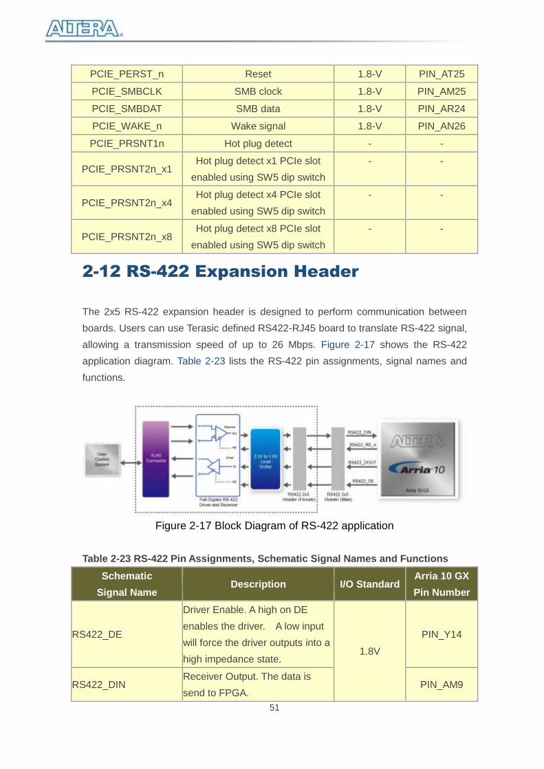
The 2x5 RS-422 expansion header is designed to perform communication between
boards. Users can use Terasic defined RS422-RJ45 board to translate RS-422 signal,
allowing a transmission speed of up to 26 Mbps. Figure 2-17 shows the RS-422
application diagram. Table 2-23 lists the RS-422 pin assignments, signal names and
functions.
Figure 2-17 Block Diagram of RS-422 application
Table 2-23 RS-422 Pin Assignments, Schematic Signal Names and Functions
Schematic
Signal Name Description I/O Standard
Arria 10 GX
Pin Number
RS422_DE
Driver Enable. A high on DE
enables the driver. A low input
will force the driver outputs into a
high impedance state. 1.8V
PIN_Y14
RS422_DIN Receiver Output. The data is
send to FPGA. PIN_AM9
52
RS422_DOUT Driver Input. The data is sent
from FPGA. PIN_W14
RS422_RE_n
Receiver Enable. A low enables
the receiver. A high input forces
the receiver output into a high
impedance state.
PIN_AD9
53
Chapter 3
System Builder
his chapter describes how users can create a custom design project for the
FPGA board from a software tool named System Builder.
3.1 Introduction
The System Builder is a Windows based software utility. It is designed to help users
create a Quartus II project for the FPGA board within minutes. The Quartus II project
files generated include:
Quartus II Project File (.qpf)
Quartus II Setting File (.qsf)
Top-Level Design File (.v)
External PLL Controller (.v)
Synopsis Design Constraints file (.sdc)
Pin Assignment Document (.htm)
The System Builder not only can generate the files above, but can also provide error-
checking rules to handle situation that are prone to errors. The common mistakes that
users encounter are the following:
Board damaged for wrong pin/bank voltage assignment.
Board malfunction caused by wrong device connections or missing pin counts
for connected ends.
Performance dropped because of improper pin assignments
T
54
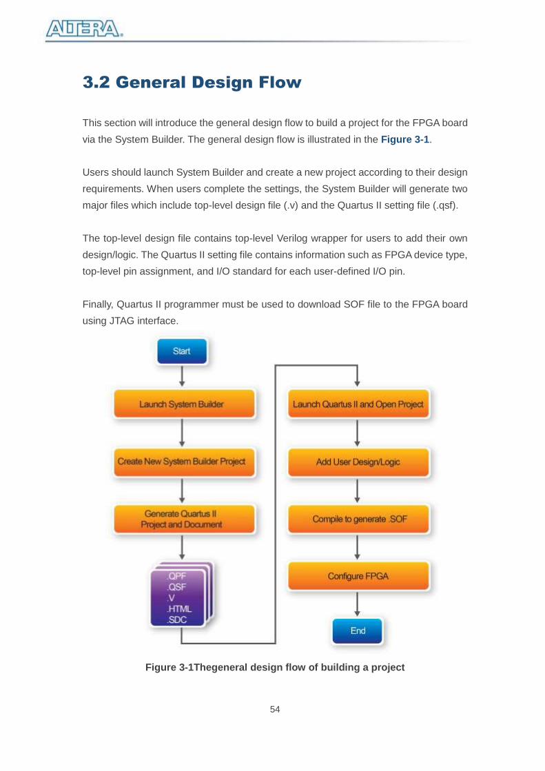
3.2 General Design Flow
This section will introduce the general design flow to build a project for the FPGA board
via the System Builder. The general design flow is illustrated in the Figure 3-1.
Users should launch System Builder and create a new project according to their design
requirements. When users complete the settings, the System Builder will generate two
major files which include top-level design file (.v) and the Quartus II setting file (.qsf).
The top-level design file contains top-level Verilog wrapper for users to add their own
design/logic. The Quartus II setting file contains information such as FPGA device type,
top-level pin assignment, and I/O standard for each user-defined I/O pin.
Finally, Quartus II programmer must be used to download SOF file to the FPGA board
using JTAG interface.
Figure 3-1Thegeneral design flow of building a project
55
3.3 Using System Builder
This section provides the detail procedures on how the System Builder is used.
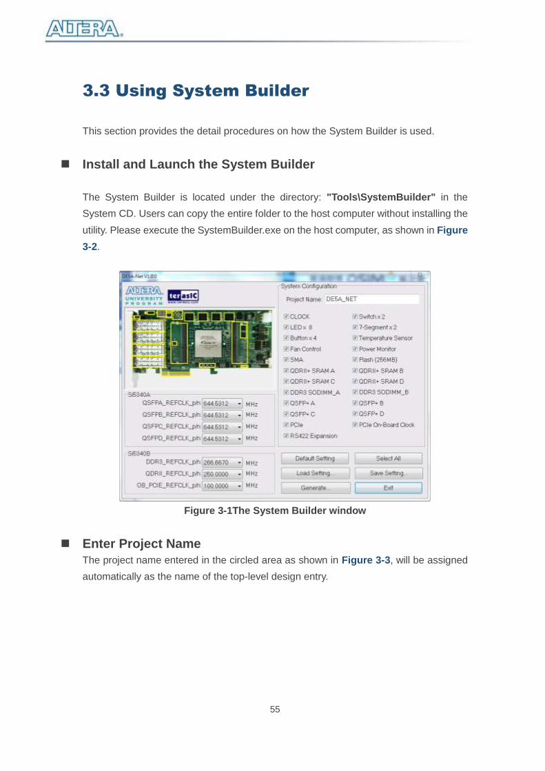
Install and Launch the System Builder
The System Builder is located under the directory: "Tools\SystemBuilder" in the
System CD. Users can copy the entire folder to the host computer without installing the
utility. Please execute the SystemBuilder.exe on the host computer, as shown in Figure
3-2.
Figure 3-1The System Builder window
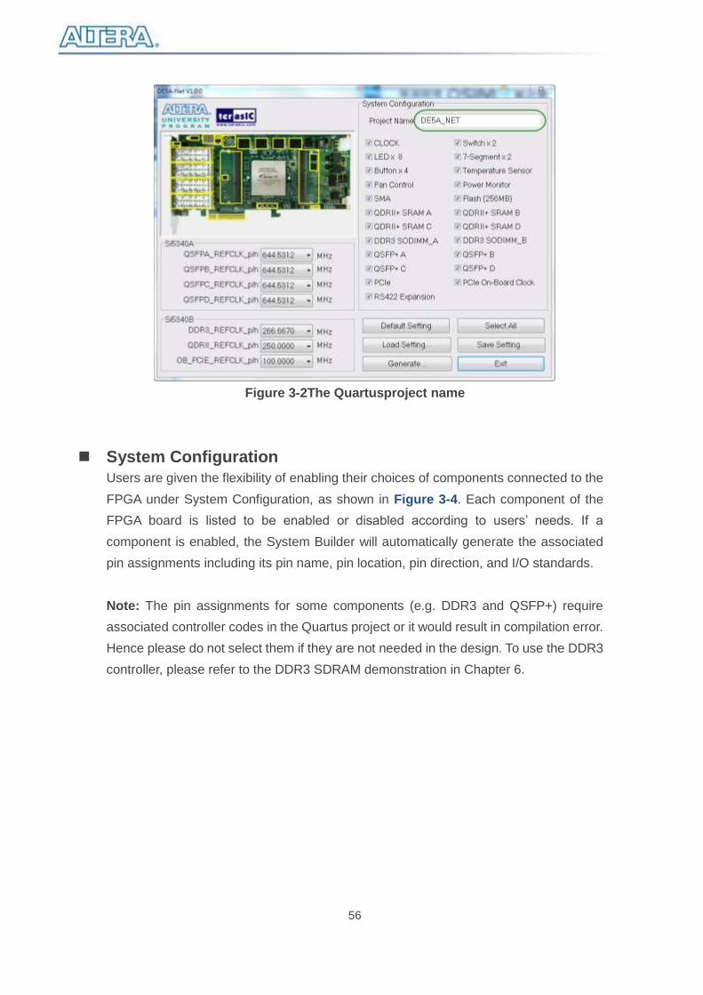
Enter Project Name
The project name entered in the circled area as shown in Figure 3-3, will be assigned
automatically as the name of the top-level design entry.
56
Figure 3-2The Quartusproject name
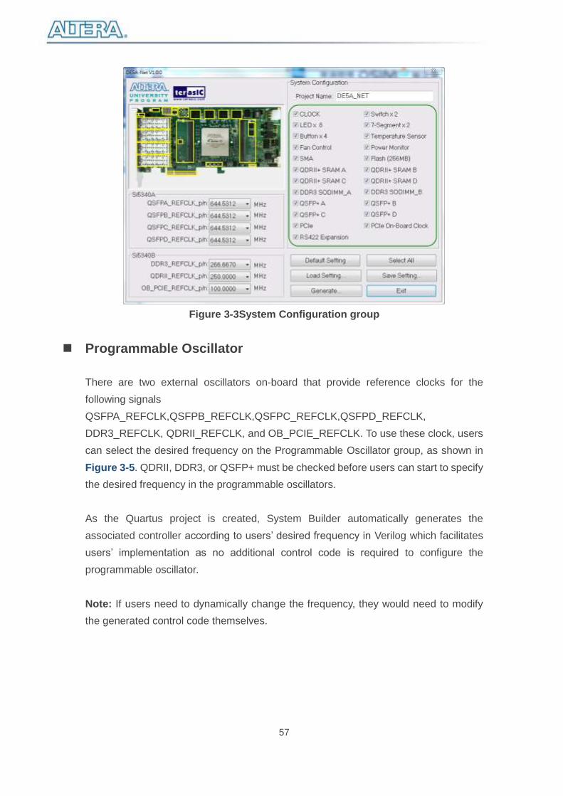
System Configuration
Users are given the flexibility of enabling their choices of components connected to the
FPGA under System Configuration, as shown in Figure 3-4. Each component of the
FPGA board is listed to be enabled or disabled according to users’ needs. If a
component is enabled, the System Builder will automatically generate the associated
pin assignments including its pin name, pin location, pin direction, and I/O standards.
Note: The pin assignments for some components (e.g. DDR3 and QSFP+) require
associated controller codes in the Quartus project or it would result in compilation error.
Hence please do not select them if they are not needed in the design. To use the DDR3
controller, please refer to the DDR3 SDRAM demonstration in Chapter 6.
57
Figure 3-3System Configuration group
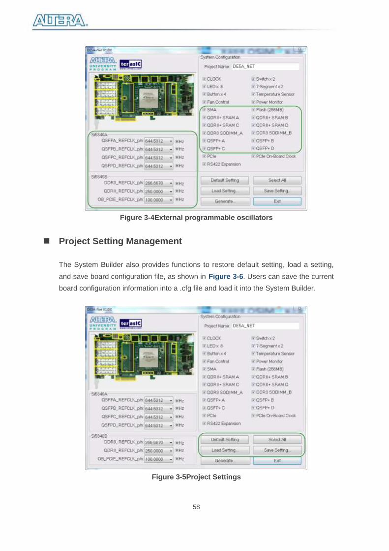
Programmable Oscillator
There are two external oscillators on-board that provide reference clocks for the
following signals
QSFPA_REFCLK,QSFPB_REFCLK,QSFPC_REFCLK,QSFPD_REFCLK,
DDR3_REFCLK, QDRII_REFCLK, and OB_PCIE_REFCLK. To use these clock, users
can select the desired frequency on the Programmable Oscillator group, as shown in
Figure 3-5. QDRII, DDR3, or QSFP+ must be checked before users can start to specify
the desired frequency in the programmable oscillators.
As the Quartus project is created, System Builder automatically generates the
associated controller according to users’ desired frequency in Verilog which facilitates
users’ implementation as no additional control code is required to configure the
programmable oscillator.
Note: If users need to dynamically change the frequency, they would need to modify
the generated control code themselves.
58
Figure 3-4External programmable oscillators
Project Setting Management
The System Builder also provides functions to restore default setting, load a setting,
and save board configuration file, as shown in HFigure 3-6. Users can save the current
board configuration information into a .cfg file and load it into the System Builder.
Figure 3-5Project Settings
59
Project Generation
When users press the Generate button, the System Builder will generate the
corresponding Quartus II files and documents as listed in theTable 3-1 in the directory
specified by the user.
Table 3-1 Files generated by the System Builder
No. Filename Description
1 <Project name>.v Top Level Verilog File for Quartus II
2 Si5340_controller (*) Si5340A and Si5340BExternal Oscillator Controller IP
3 <Project name>.qpf Quartus II Project File
4 <Project name>.qsf Quartus II Setting File
5 <Project name>.sdc Synopsis Design Constraints File for Quartus II
6 <Project name>.htm Pin Assignment Document
(*) The Si5340_controller is a folder which contains the Verilog files for the configuration
of Si5340A and Si5340B.
Users can add custom logic into the project and compile the project in Quartus II to
generate the SRAM Object File (.sof).
For Si5340A, its controller will be instantiated in the Quartus II top-level file, as listed
below:
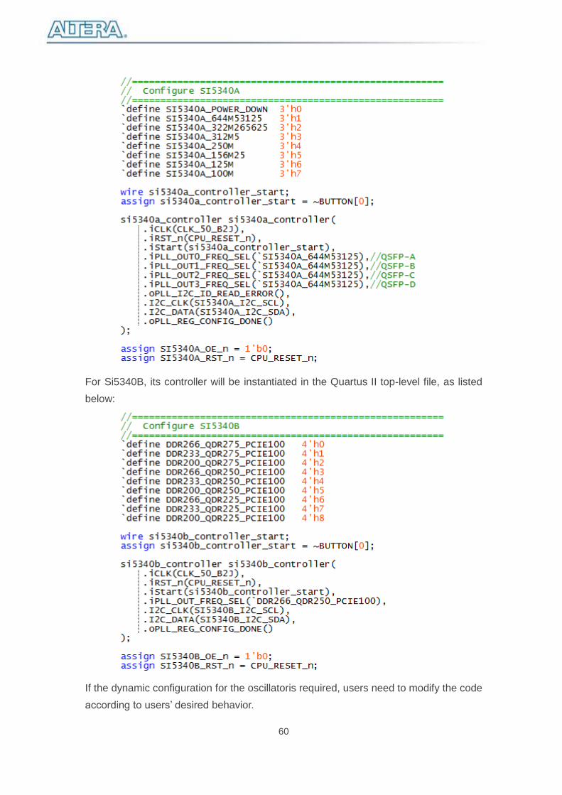
60
For Si5340B, its controller will be instantiated in the Quartus II top-level file, as listed
below:
If the dynamic configuration for the oscillatoris required, users need to modify the code
according to users’ desired behavior.
61
Chapter 4
Flash Programming
s you develop your own project using the Altera tools, you can program the
flash memory device so that your own design loads from flash memory into the
FPGA on power up. This chapter will describe how to use Altera Quartus II
Programmer Tool to program the common flash interface (CFI) flash memory device on
the FPGA board. The Arria X GX FPGA development board ships with the CFI flash
device preprogrammed with a default factory FPGA configuration for running the
Parallel Flash Loader design example.
4.1 CFI Flash Memory Map
Table 4-1shows the default memory contents of two interlaced 1Gb (128MB) CFI flash
device. Each flash device has a 16-bit data bus and the two combined flash devices
allow for a 32-bit flash memory interface. For the factory default code to run correctly
and update designs in the user memory, this memory map must not be altered.
Table 4-1Flash Memory Map (Byte Address)
Block Description Size(KB) Address Range
PFL option bits 64 0x00030000 – 0x0003FFFF
Factory hardware 44,032 0x00040000 – 0x02B3FFFF
User hardware 44,032 0x02B40000 – 0x0563FFFF
Factory software 8,192 0x05640000 – 0x05E3FFFF
User software and data 165,632 0x05E40000 – 0x0FFFFFFF
For user application, user hardware must be stored with start address 0x02B40000, and
the user’s software is suggested to be stored with start address 0x05E40000. The NIOS
II EDS tool nios-2-flash-programmer is used for programming the flash. Before
programming, users need to translate their Quartus .sof and NIOS II .elf files into
the .flash which is used by the nios-2-flash-programmer. For .sof to .flash translation,
NIOS II EDS tool sof2flsh can be used. For the .elf to .flash translation, NIOS II EDS
tool elf2flash can be used. For convenience, the System CD contains a batch file for file
A
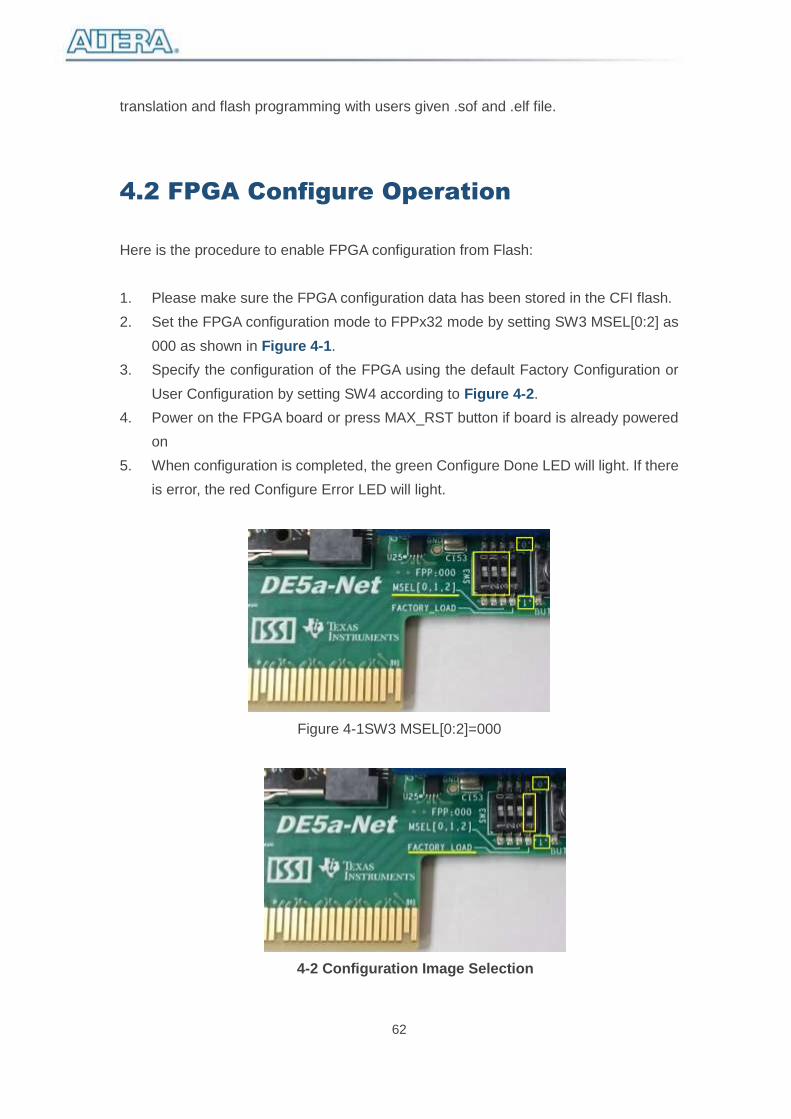
62
translation and flash programming with users given .sof and .elf file.
4.2 FPGA Configure Operation
Here is the procedure to enable FPGA configuration from Flash:
1. Please make sure the FPGA configuration data has been stored in the CFI flash.
2. Set the FPGA configuration mode to FPPx32 mode by setting SW3 MSEL[0:2] as
000 as shown in Figure 4-1.
3. Specify the configuration of the FPGA using the default Factory Configuration or
User Configuration by setting SW4 according to Figure 4-2.
4. Power on the FPGA board or press MAX_RST button if board is already powered
on
5. When configuration is completed, the green Configure Done LED will light. If there
is error, the red Configure Error LED will light.
Figure 4-1SW3 MSEL[0:2]=000
4-2 Configuration Image Selection
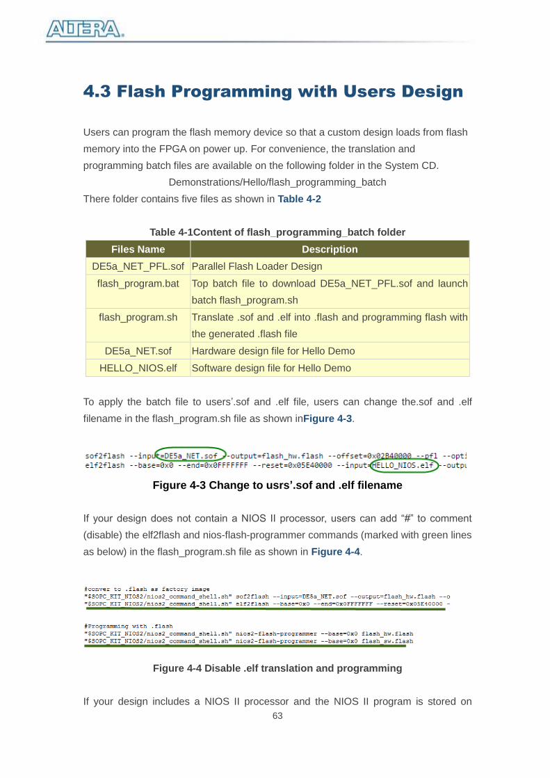
63
4.3 Flash Programming with Users Design
Users can program the flash memory device so that a custom design loads from flash
memory into the FPGA on power up. For convenience, the translation and
programming batch files are available on the following folder in the System CD.
Demonstrations/Hello/flash_programming_batch
There folder contains five files as shown in Table 4-2
Table 4-1Content of flash_programming_batch folder
Files Name Description
DE5a_NET_PFL.sof Parallel Flash Loader Design
flash_program.bat Top batch file to download DE5a_NET_PFL.sof and launch
batch flash_program.sh
flash_program.sh Translate .sof and .elf into .flash and programming flash with
the generated .flash file
DE5a_NET.sof Hardware design file for Hello Demo
HELLO_NIOS.elf Software design file for Hello Demo
To apply the batch file to users’.sof and .elf file, users can change the.sof and .elf
filename in the flash_program.sh file as shown inFigure 4-3.
Figure 4-3 Change to usrs’.sof and .elf filename
If your design does not contain a NIOS II processor, users can add “#” to comment
(disable) the elf2flash and nios-flash-programmer commands (marked with green lines
as below) in the flash_program.sh file as shown in Figure 4-4.
Figure 4-4 Disable .elf translation and programming
If your design includes a NIOS II processor and the NIOS II program is stored on
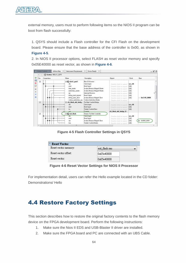
64
external memory, users must to perform following items so the NIOS II program can be
boot from flash successfully:
1. QSYS should include a Flash controller for the CFI Flash on the development
board. Please ensure that the base address of the controller is 0x00, as shown in
Figure 4-5.
2. In NIOS II processor options, select FLASH as reset vector memory and specify
0x05E40000 as reset vector, as shown in Figure 4-6.
Figure 4-5 Flash Controller Settings in QSYS
Figure 4-6 Reset Vector Settings for NIOS II Processor
For implementation detail, users can refer the Hello example located in the CD folder:
Demonstrations/ Hello
4.4 Restore Factory Settings
This section describes how to restore the original factory contents to the flash memory
device on the FPGA development board. Perform the following instructions:
1. Make sure the Nios II EDS and USB-Blaster II driver are installed.
2. Make sure the FPGA board and PC are connected with an UBS Cable.

65
3. Power on the FPGA board.
4. Copy the “Demonstrations/PFL/flash_programming_batch” folder under the
CD to your PC’s local drive.
5. Execute the batch file flash_program.bat to start flash programming.
6. Power off the FPGA Board.
7. Set FPGA configure mode as FPPx32 Mode by setting SW3 MSEL[0:2] to
000.
8. Specify configuration of the FPGA to Factory Hardware by setting the
FACTORY_LOAD dip in SW4 to the ‘1’ position.
9. Power on the FPGA Board, and the Configure Done LED should light.
Except for programming the Flash with the default code PFL, the batch file also writes
PFL (Parallel Flash Loader) Option Bits data into the address 0x30000. The option bits
data specifies 0x2B40000 as start address of your hardware design.
The NIOS II EDS tool nios-2-flash-programmer programs the Flash based on the
Parallel Flasher Loader design in the FPGA. The Parallel Flash Loader design is
included in the default code PFL and the source code is available in the folder
Demonstrations/ PFL in System CD.
Chapter 5
Peripheral Reference
Design
his chapter introduces DE5a-NET peripheral interface reference designs. It
mainly introduces Si5340 chip which is a programmable clock generator. We
provide two ways (Pure RTL IP and NIOS/Qsys System) respectively to show
how to control Si5340 to output desired frequencies, as well as how to control the fan
speed. The source codes and tool of these examples are all available on the System
CD.
T
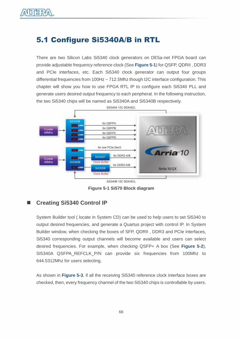
66
5.1 Configure Si5340A/B in RTL
There are two Silicon Labs Si5340 clock generators on DE5a-net FPGA board can
provide adjustable frequency reference clock (See Figure 5-1) for QSFP, QDRII , DDR3
and PCIe interfaces, etc. Each Si5340 clock generator can output four groups
differential frequencies from 100Hz ~ 712.5Mhz though I2C interface configuration. This
chapter will show you how to use FPGA RTL IP to configure each Si5340 PLL and
generate users desired output frequency to each peripheral. In the following instruction,
the two Si5340 chips will be named as Si5340A and Si5340B respectively.
Figure 5-1 Si570 Block diagram
Creating Si5340 Control IP
System Builder tool ( locate in System CD) can be used to help users to set Si5340 to
output desired frequencies, and generate a Quartus project with control IP. In System
Builder window, when checking the boxes of SFP, QDRII , DDR3 and PCIe interfaces,
Si5340 corresponding output channels will become available and users can select
desired frequencies. For example, when checking QSFP+ A box (See Figure 5-2),
SI5340A QSFPA_REFCLK_P/N can provide six frequencies from 100Mhz to
644.5312Mhz for users selecting.
As shown in Figure 5-3, if all the receiving Si5340 reference clock interface boxes are
checked, then, every frequency channel of the two Si5340 chips is controllable by users.
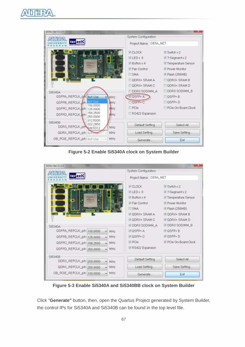
67
Figure 5-2 Enable Si5340A clock on System Builder
Figure 5-3 Enable Si5340A and Si5340BB clock on System Builder
Click "Generate" button, then, open the Quartus Project generated by System Builder,
the control IPs for Si5340A and Si5340B can be found in the top level file.
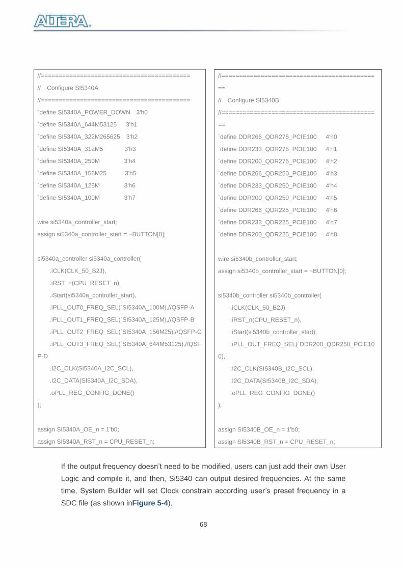
68
If the output frequency doesn’t need to be modified, users can just add their own User
Logic and compile it, and then, Si5340 can output desired frequencies. At the same
time, System Builder will set Clock constrain according user’s preset frequency in a
SDC file (as shown inFigure 5-4).
//==========================================
// Configure SI5340A
//==========================================
`define SI5340A_POWER_DOWN 3'h0
`define SI5340A_644M53125 3'h1
`define SI5340A_322M265625 3'h2
`define SI5340A_312M5 3'h3
`define SI5340A_250M 3'h4
`define SI5340A_156M25 3'h5
`define SI5340A_125M 3'h6
`define SI5340A_100M 3'h7
wire si5340a_controller_start;
assign si5340a_controller_start = ~BUTTON[0];
si5340a_controller si5340a_controller(
.iCLK(CLK_50_B2J),
.iRST_n(CPU_RESET_n),
.iStart(si5340a_controller_start),
.iPLL_OUT0_FREQ_SEL(`SI5340A_100M),//QSFP-A
.iPLL_OUT1_FREQ_SEL(`SI5340A_125M),//QSFP-B
.iPLL_OUT2_FREQ_SEL(`SI5340A_156M25),//QSFP-C
.iPLL_OUT3_FREQ_SEL(`SI5340A_644M53125),//QSF
P-D
.I2C_CLK(SI5340A_I2C_SCL),
.I2C_DATA(SI5340A_I2C_SDA),
.oPLL_REG_CONFIG_DONE()
);
assign SI5340A_OE_n = 1'b0;
assign SI5340A_RST_n = CPU_RESET_n;
//===========================================
==
// Configure SI5340B
//===========================================
==
`define DDR266_QDR275_PCIE100 4'h0
`define DDR233_QDR275_PCIE100 4'h1
`define DDR200_QDR275_PCIE100 4'h2
`define DDR266_QDR250_PCIE100 4'h3
`define DDR233_QDR250_PCIE100 4'h4
`define DDR200_QDR250_PCIE100 4'h5
`define DDR266_QDR225_PCIE100 4'h6
`define DDR233_QDR225_PCIE100 4'h7
`define DDR200_QDR225_PCIE100 4'h8
wire si5340b_controller_start;
assign si5340b_controller_start = ~BUTTON[0];
si5340b_controller si5340b_controller(
.iCLK(CLK_50_B2J),
.iRST_n(CPU_RESET_n),
.iStart(si5340b_controller_start),
.iPLL_OUT_FREQ_SEL(`DDR200_QDR250_PCIE10
0),
.I2C_CLK(SI5340B_I2C_SCL),
.I2C_DATA(SI5340B_I2C_SDA),
.oPLL_REG_CONFIG_DONE()
);
assign SI5340B_OE_n = 1'b0;
assign SI5340B_RST_n = CPU_RESET_n;
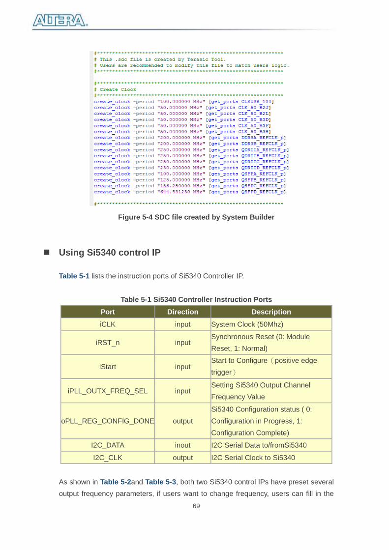
69
Figure 5-4 SDC file created by System Builder
Using Si5340 control IP
Table 5-1 lists the instruction ports of Si5340 Controller IP.
Table 5-1 Si5340 Controller Instruction Ports
Port Direction Description
iCLK input System Clock (50Mhz)
iRST_n input Synchronous Reset (0: Module
Reset, 1: Normal)
iStart input Start to Configure(positive edge
trigger)
iPLL_OUTX_FREQ_SEL input Setting Si5340 Output Channel
Frequency Value
oPLL_REG_CONFIG_DONE output
Si5340 Configuration status ( 0:
Configuration in Progress, 1:
Configuration Complete)
I2C_DATA inout I2C Serial Data to/fromSi5340
I2C_CLK output I2C Serial Clock to Si5340
As shown in Table 5-2and Table 5-3, both two Si5340 control IPs have preset several
output frequency parameters, if users want to change frequency, users can fill in the
70
input port " iPLL_OUTX_FREQ_SEL" with a desired frequency value and recompile the
project. For example, in Si5340A control IP, change
.iPLL_OUT1_FREQ_SEL(`SI5340A_125M),
to
.iPLL_OUT1_FREQ_SEL(`SI5340A_156M25),
Recompile project, the Si5340A OUT2 channel (for QSFP-C ) output frequency will
change from 125Mhz to 156.25Mhz.
Table 5-2 Si5340A Controller Frequency Setting
iPLL_OUTX_FREQ_SEL
MODE Setting Si5340A Channel Clock Frequency(MHz)
3'b000 Power Down
3'b001 644.53125
3'b010 322.26
3'b011 312.25
3'b100 250
3'b101 156.25
3'b110 125
3'b111 100
Table 5-3 Si5340B Controller Frequency Setting
iPLL_OUT_FRE
Q_SEL MODE
Setting
DDR3
Frequency(MHz)
QDRII
Frequency(MHz)
PCIE
Frequency(MHz)
4'b0000 266 275 100
4'b0001 233 275 100
4'b0010 200 275 100
4'b0011 266 250 100
4'b0100 233 250 100
4'b0101 200 250 100
4'b0110 266 225 100
4'b0111 233 225 100
4'b1000 200 225 100
Users can also dynamically modify the input parameters, and input a positive edge

71
trigger for “iStart”, then, Si5340 output frequency can be modified.
After the manually modifying, please remember to modify the corresponding frequency
value in SDC file.
Modify Clock Parameter For Your Own Frequency
If the Si5340 control IP build-in frequencies are not users’ desired, users can refer to
below steps to modify control IP register parameter settings to modify the IP to output a
desired frequency.
1. Firstly, download ClockBuider Pro Software (See Figure 5-5), which is provided
by Silicon Labs. This tool can help users to set the Si5340’s output frequency of
each channel through the GUI interface, and it will automatically calculate the
Register parameters required for each frequency. The tool download link:
http://www.silabs.com/products/clocksoscillators/pages/timing-software-
development-tools.aspx
Figure 5-5 ClockBuilder Pro Wizard
72
2. After the installation, select Si5340, and configure the input frequency and output
frequency as shown in Figure 5-6.
Figure 5-6 Define Output Clock Frequencies on ClockBuilder Pro Wizard
3. After the setting is completed, ClockBuider Pro Wizard generates a Design
Report(text), which contains users setting frequency corresponding register
value (See Figure 5-7).
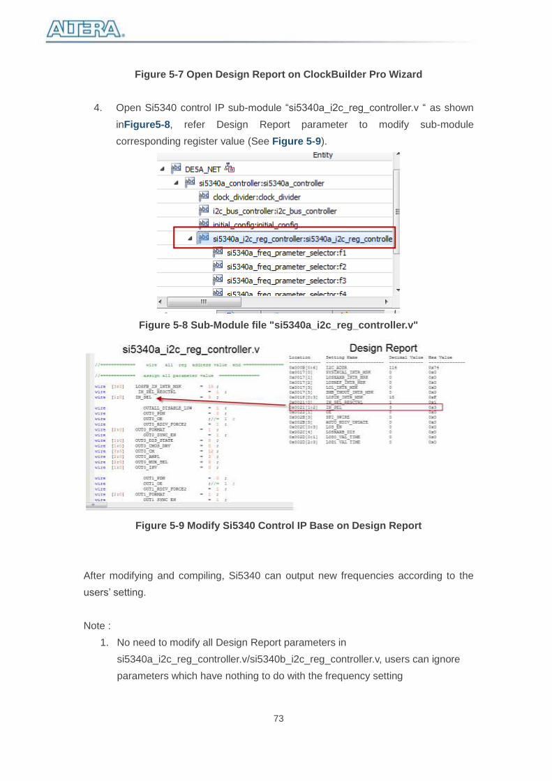
73
Figure 5-7 Open Design Report on ClockBuilder Pro Wizard
4. Open Si5340 control IP sub-module “si5340a_i2c_reg_controller.v “ as shown
inFigure5-8, refer Design Report parameter to modify sub-module
corresponding register value (See Figure 5-9).
Figure 5-8 Sub-Module file "si5340a_i2c_reg_controller.v"
Figure 5-9 Modify Si5340 Control IP Base on Design Report
After modifying and compiling, Si5340 can output new frequencies according to the
users’ setting.
Note :
1. No need to modify all Design Report parameters in
si5340a_i2c_reg_controller.v/si5340b_i2c_reg_controller.v, users can ignore
parameters which have nothing to do with the frequency setting
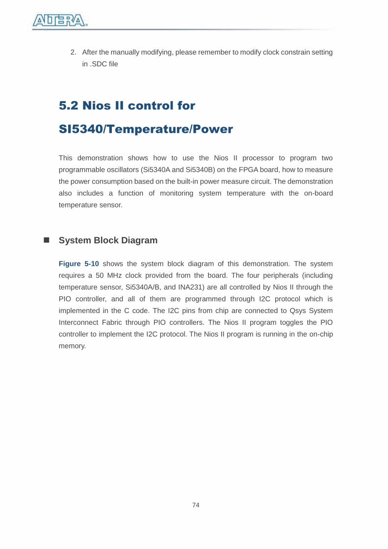
74
2. After the manually modifying, please remember to modify clock constrain setting
in .SDC file
5.2 Nios II control for
SI5340/Temperature/Power
This demonstration shows how to use the Nios II processor to program two
programmable oscillators (Si5340A and Si5340B) on the FPGA board, how to measure
the power consumption based on the built-in power measure circuit. The demonstration
also includes a function of monitoring system temperature with the on-board
temperature sensor.
System Block Diagram
Figure 5-10 shows the system block diagram of this demonstration. The system
requires a 50 MHz clock provided from the board. The four peripherals (including
temperature sensor, Si5340A/B, and INA231) are all controlled by Nios II through the
PIO controller, and all of them are programmed through I2C protocol which is
implemented in the C code. The I2C pins from chip are connected to Qsys System
Interconnect Fabric through PIO controllers. The Nios II program toggles the PIO
controller to implement the I2C protocol. The Nios II program is running in the on-chip
memory.
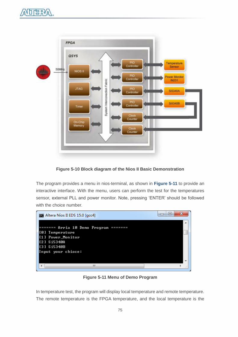
75
Figure 5-10 Block diagram of the Nios II Basic Demonstration
The program provides a menu in nios-terminal, as shown in Figure 5-11 to provide an
interactive interface. With the menu, users can perform the test for the temperatures
sensor, external PLL and power monitor. Note, pressing ‘ENTER’ should be followed
with the choice number.
Figure 5-11 Menu of Demo Program
In temperature test, the program will display local temperature and remote temperature.
The remote temperature is the FPGA temperature, and the local temperature is the

76
board temperature where the temperature sensor located.
A power monitor IC (INA231AIYFFT) embedded on the board can monitor Arria10 real-
time current and power. This IC can work out current/power value as multiplier and
divider are embedded in it. There is a shunt resistor R149 (RSHUNT =0.003 Ω) for
INA231AIYFFT in the circuit, when power on the DE5a-NET board, there will be a
voltage drop (named Shut Voltage) on R149. Based on sense resistors, the program of
power monitor can calculate the associated voltage, current and power consumption
from the IN231 through the I2C interface. Please note the device I2C address is 0x80.
In the external PLL programming test, the program will program the PLL first, and
subsequently will use TERASIC QSYS custom CLOCK_COUNTER IP to count the
clock count in a specified period to check whether the output frequency is changed as
configured. To avoid a Quartus II compilation error, dummy transceiver controllers are
created to receive the clock from the external PLL. Users can ignore the functionality of
the transceiver controller in the demonstration. For Si5340A/B programming, Please
note the device I2C address are 0xEE. The program can control the Si5340A to
configure the output frequency of QSFPA/B/C/D REFCLK, or control the Si5340B to
configure the output frequency of DDR3/PCIE/QDRII REFCLK according to your choice.
Demonstration File Locations
Hardware project directory: NIOS_BASIC_DEMO
Bitstream used: NIOS_BASIC_DEMO.sof
Software project directory: NIOS_BASIC_DEMO \software
Demo batch file : NIOS_BASIC_DEMO\demo_batch\NIOS_BASIC_DEMO.bat,
NIOS_BASIC_DEMO.sh
Demonstration Setup and Instructions
Make sure Quartus II and Nios II are installed on your PC.
Power on the FPGA board.
Use the USB Cable to connect your PC and the FPGA board and install USB
Blaster II driver if necessary.
Execute the demo batch file “NIOS_BASIC_DEMO.bat” under the batch file folder,
NIOS_BASIC_DEMO\demo_batch.
After the Nios II program is downloaded and executed successfully, a prompt
message will be displayed in nios2-terminal.
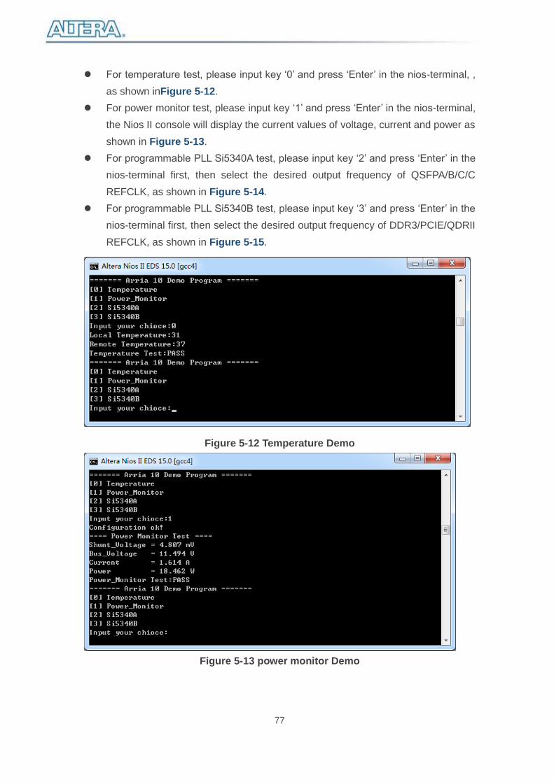
77
For temperature test, please input key ‘0’ and press ‘Enter’ in the nios-terminal, ,
as shown inFigure 5-12.
For power monitor test, please input key ‘1’ and press ‘Enter’ in the nios-terminal,
the Nios II console will display the current values of voltage, current and power as
shown in Figure 5-13.
For programmable PLL Si5340A test, please input key ‘2’ and press ‘Enter’ in the
nios-terminal first, then select the desired output frequency of QSFPA/B/C/C
REFCLK, as shown in Figure 5-14.
For programmable PLL Si5340B test, please input key ‘3’ and press ‘Enter’ in the
nios-terminal first, then select the desired output frequency of DDR3/PCIE/QDRII
REFCLK, as shown in Figure 5-15.
Figure 5-12 Temperature Demo
Figure 5-13 power monitor Demo
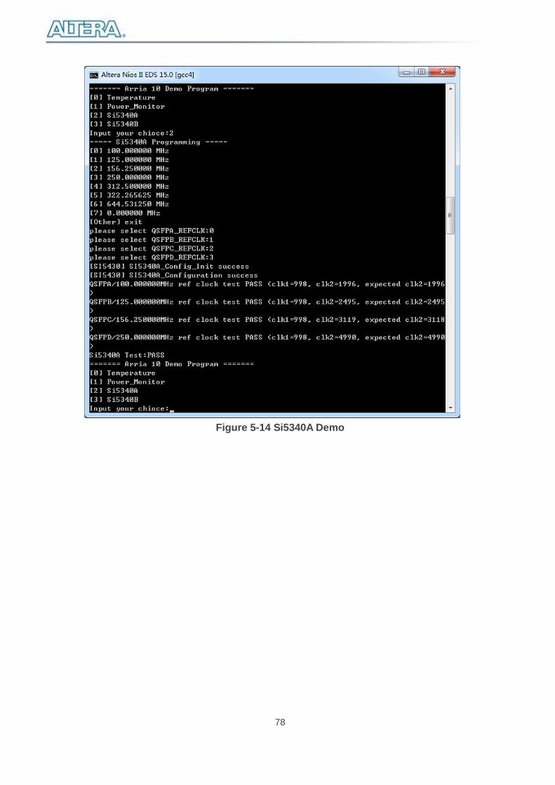
78
Figure 5-14 Si5340A Demo
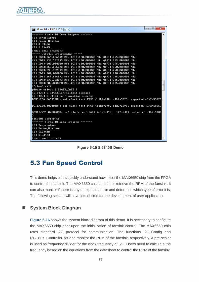
79
Figure 5-15 Si5340B Demo
5.3 Fan Speed Control
This demo helps users quickly understand how to set the MAX6650 chip from the FPGA
to control the fansink. The MAX6650 chip can set or retrieve the RPM of the fansink. It
can also monitor if there is any unexpected error and determine which type of error it is.
The following section will save lots of time for the development of user application.
System Block Diagram
Figure 5-16 shows the system block diagram of this demo. It is necessary to configure
the MAX6650 chip prior upon the initialization of fansink control. The MAX6650 chip
uses standard I2C protocol for communication. The functions I2C_Config and
I2C_Bus_Controller set and monitor the RPM of the fansink, respectively. A pre-scaler
is used as frequency divider for the clock frequency of I2C. Users need to calculate the
frequency based on the equations from the datasheet to control the RPM of the fansink.
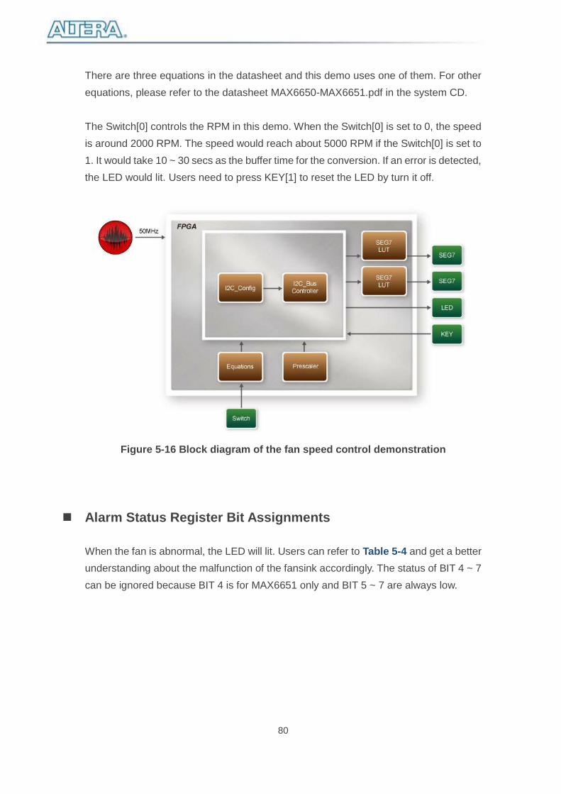
80
There are three equations in the datasheet and this demo uses one of them. For other
equations, please refer to the datasheet MAX6650-MAX6651.pdf in the system CD.
The Switch[0] controls the RPM in this demo. When the Switch[0] is set to 0, the speed
is around 2000 RPM. The speed would reach about 5000 RPM if the Switch[0] is set to
1. It would take 10 ~ 30 secs as the buffer time for the conversion. If an error is detected,
the LED would lit. Users need to press KEY[1] to reset the LED by turn it off.
Figure 5-16 Block diagram of the fan speed control demonstration
Alarm Status Register Bit Assignments
When the fan is abnormal, the LED will lit. Users can refer to Table 5-4 and get a better
understanding about the malfunction of the fansink accordingly. The status of BIT 4 ~ 7
can be ignored because BIT 4 is for MAX6651 only and BIT 5 ~ 7 are always low.
81
Table 5-4 Alarm-Enable Resgister Bit Masks
Design Tools
64-bit Quartus II v15.1
Demonstration Source Code
Project Directory: Demonstration\Fan
Bit Stream: DE5a_NET_golden_top.sof
Demonstration Batch File
Demo Batch File Folder: \Fan\demo_batch
The demo batch file includes following files:
Batch File: test_ub2.bat
FPGA Configure File: DE5a_NET_folden_top.sof
Demonstration Setup
Make sure Quartus II is installed on the host PC.
Connect the DE5a-Net and the host PC via USB cable. Install the USB-Blaster II
driver if necessary.
Power on the FPGA Board.
Execute the demo batch file “test_ub2.bat” under the batch file folder
\Fan\demo_batch.
When SW[0] is set to 0, the RPM would slowly be adjusted to ~2000. When SW[0]
is set to 1, the RPM would slowly be adjusted to ~5000.
BIT NAME POR(DEFAULT)S
TATE FUNCTION
7(MSB) to 5 --- 0 Always 0
4 GPIO2
(MAX6651 only) 0
GPIO2 Alarm. Set when GPIO2
is low (MAX6651 only)
3(LED[3]) GPIO1 0 GPIO1 Alarm. Set when GPIO1
is low
2(LED[2]) TACH 0 Tachometer Overflow Alarm
1(LED[1]) MIN 0 Minimum Output Level Alarm
0(LED[0]) MAX 0 Maximum Output Level Alarm
82
Chapter 6
Memory Reference
Design
he FPGA development board includes two kinds of high-speed memories:
DDR3 SDRAM: two independent banks, update to 1066 MHz
QDRII+ SRAM: four independent banks, update to 550 MHz
This chapter will show three examples which use the Altera Memory IP to perform
memory test functions. The source codes of these examples are all available on the
FPGA System CD. These three examples are:
QDRII+ SRAM Test: Full test of the four banks of QDRII+ SRAM
DD3 SDRAM Test: Random test of the two banks of DDR3 SDRAM.
DDR3 SDRAM Test by Nios II: Full test of one bank of DDR3 SDRAM with
Nios II
Note. 64-Bit Quartus15.0 or later is strongly recommended for compiling these projects.
6.1 QDRII+ SRAM Test
QDR II/QDR II+ SRAM devices enable you to maximize memory bandwidth with
separate read and write ports. The memory architecture features separate read and
write ports operating twice per clock cycle to deliver a total of four data transfers per
cycle. The resulting performance increase is particularly valuable in bandwidth-
intensive and low-latency applications.
This demonstration utilizes four QDRII+ SRAMs on the FPGA board. It describes how
to use Altera’s “Arria 10 External Memory Interfaces” (Arria 10 EMIF) IP to implement a
T
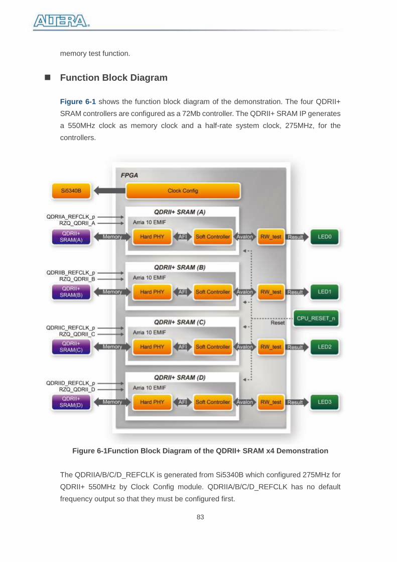
83
memory test function.
Function Block Diagram
Figure 6-1 shows the function block diagram of the demonstration. The four QDRII+
SRAM controllers are configured as a 72Mb controller. The QDRII+ SRAM IP generates
a 550MHz clock as memory clock and a half-rate system clock, 275MHz, for the
controllers.
Figure 6-1Function Block Diagram of the QDRII+ SRAM x4 Demonstration
The QDRIIA/B/C/D_REFCLK is generated from Si5340B which configured 275MHz for
QDRII+ 550MHz by Clock Config module. QDRIIA/B/C/D_REFCLK has no default
frequency output so that they must be configured first.
84
In this demonstration, each QDRII+ SRAM has its own PLL, DLL and OCT resources.
The Arria 10 EMIF QDRII IP uses a Hard PHY and a soft Controller. The Hard PHY
capable of performing key memory interface functionality such as read/write leveling,
FIFO buffering to lower latency and improve margin, timing calibration, and on-chip
termination.
The Avalon bus read/write test (RW_test) modules read and write the entire memory
space of each QDRII+ SRAM through the Avalon interface of each controller. In this
project, the RW_test module will first write the entire memory and then compare the
read back data with the regenerated data (the same sequence as the write data). Test
control signals for four QDRII+ SRAMs will generate from CPU_RESET_n and four
LEDs will indicate the test results of four QDRII+ SRAMs.
Altera QDRII and QDRII+ SRAM Controller with UniPHY
To use Altera QDRII+ SRAM controller, users need to perform the following steps in
order:
1. Create correct pin assignments for QDRII+.
2. Setup correct parameters in QDRII+ SRAM controller dialog.
Design Tools
Quartus II 15.1
Demonstration Source Code
Project directory: QDRIIx4_Test
Bit stream used: QDRIIx4_Test.sof
Demonstration Batch File
Demo Batch File Folder: QDRIIx4_Test\demo_batch
The demo batch files include the followings:
Batch file for USB-Blaster II: test_ub2.bat,
FPGA configuration file: QDRIIx4_Test.sof
Demonstration Setup
Make sure Quartus II is installed on your PC.
Connect the USB cable to the FPGA board and host PC. Install the USB-Blaster II
driver if necessary.
85
Power on the FPGA Board.
Execute the demo batch file “test_ub2.bat” under the batch file folder,
QDRIIx4_Test\demo_batch.
Press CPU_RESET_n of the FPGA board to start the verification process. When
CPU_RESET_n is held down, all the LEDs will be turned off. All LEDs should turn
back on to indicate test passes upon the release of CPU_RESET_n.
If any LED is not lit up after releasing CPU_RESET_n, it indicates the
corresponding QDRII+ SRAM test has failed. Table 6-1 lists the matchup for the
four LEDs.
Press CPU_RESET_n again to regenerate the test control signals for a repeat test.
Table 6-1 LED Indicators
NAME Description
LED0 QDRII+ SRAM(A) test result
LED1 QDRII+ SRAM(B) test result
LED2 QDRII+ SRAM(C) test result
LED3 QDRII+ SRAM(D) test result
6.2 DDR3 SDRAM Test
This demonstration performs a memory test function on the two DDR3-SDRAM SO-
DIMM on the DE5a-Net. The memory size of each DDR3 SDRAM SO-DIMM used in
this test is 4 GB.
Function Block Diagram
Figure 6-2 shows the function block diagram of this demonstration. There are two
DDR3 SDRAM controllers. The controller uses 266.667 MHz as a reference clock. It
generates one 1066MHz clock as memory clock from the FPGA to the memory and the
controller itself runs at quarter-rate in the FPGA i.e. 266.667MHz.
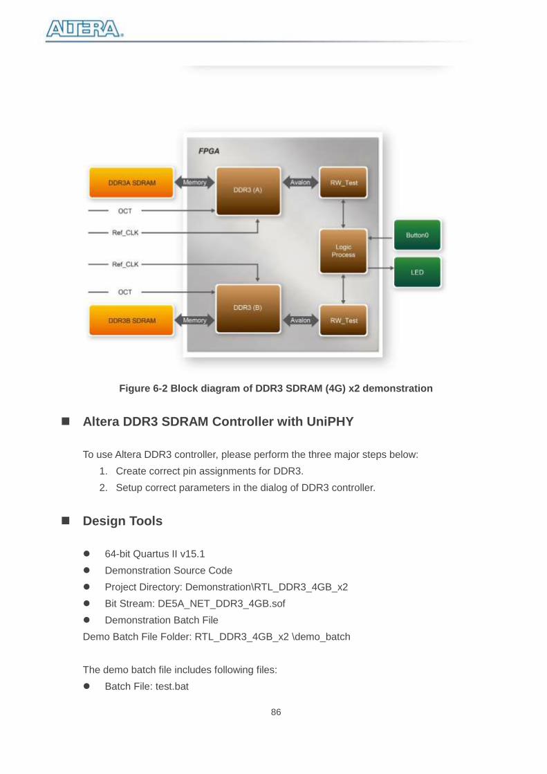
86
Figure 6-2 Block diagram of DDR3 SDRAM (4G) x2 demonstration
Altera DDR3 SDRAM Controller with UniPHY
To use Altera DDR3 controller, please perform the three major steps below:
1. Create correct pin assignments for DDR3.
2. Setup correct parameters in the dialog of DDR3 controller.
Design Tools
64-bit Quartus II v15.1
Demonstration Source Code
Project Directory: Demonstration\RTL_DDR3_4GB_x2
Bit Stream: DE5A_NET_DDR3_4GB.sof
Demonstration Batch File
Demo Batch File Folder: RTL_DDR3_4GB_x2 \demo_batch
The demo batch file includes following files:
Batch File: test.bat
87
FPGA Configuration File: DE5A_NET_4GB.sof
Demonstration Setup
Make sure Quartus II is installed on the host PC.
Connect DE5a-Net board to the host PC via USB cable. Install the USB-Blaster II
driver if necessary.
Power on the DE5a-Net board.
Execute the demo batch file “test.bat” under the batch file folder
\RTL_DDR3_4GB_x2\demo_batch.
Press BUTTON0 on DE5a-Net to start the verification process. When BUTTON0
is pressed, LED1, LED2, and LED3 should start blinking. After approximately 2
seconds, LED1 and LED2 should stop blinking and stay on to indicate the DDR3
(A) and DDR3 (B) have passed the test, respectively. Table 6-2 lists the LED
indicators.
If LED3 is not blinking, it means the 50MHz clock source is not working.
If LED1 or LED2 does not start blinking upon releasing BUTTON0, it indicates
local_cal_success of the corresponding DDR3 fails.
If LED1 or LED2 fail to remain on after 2 seconds, the corresponding DDR3 test
has failed.
Press BUTTON0 again to regenerate the test control signals for a repeat test.
Table 6-2 LED Indicators
NAME Description
LED0 Reset
LED1 DDR3 (A) test result
LED2 DDR3 (B) test result
LED3 50MHz clock source
6.3 DDR3 SDRAM Test by Nios II
Many applications use a high performance RAM, such as a DDR3 SDRAM, to provide
temporary storage. In this demonstration hardware and software designs are provided
to illustrate how to perform DDR3 memory access in QSYS. We describe how the
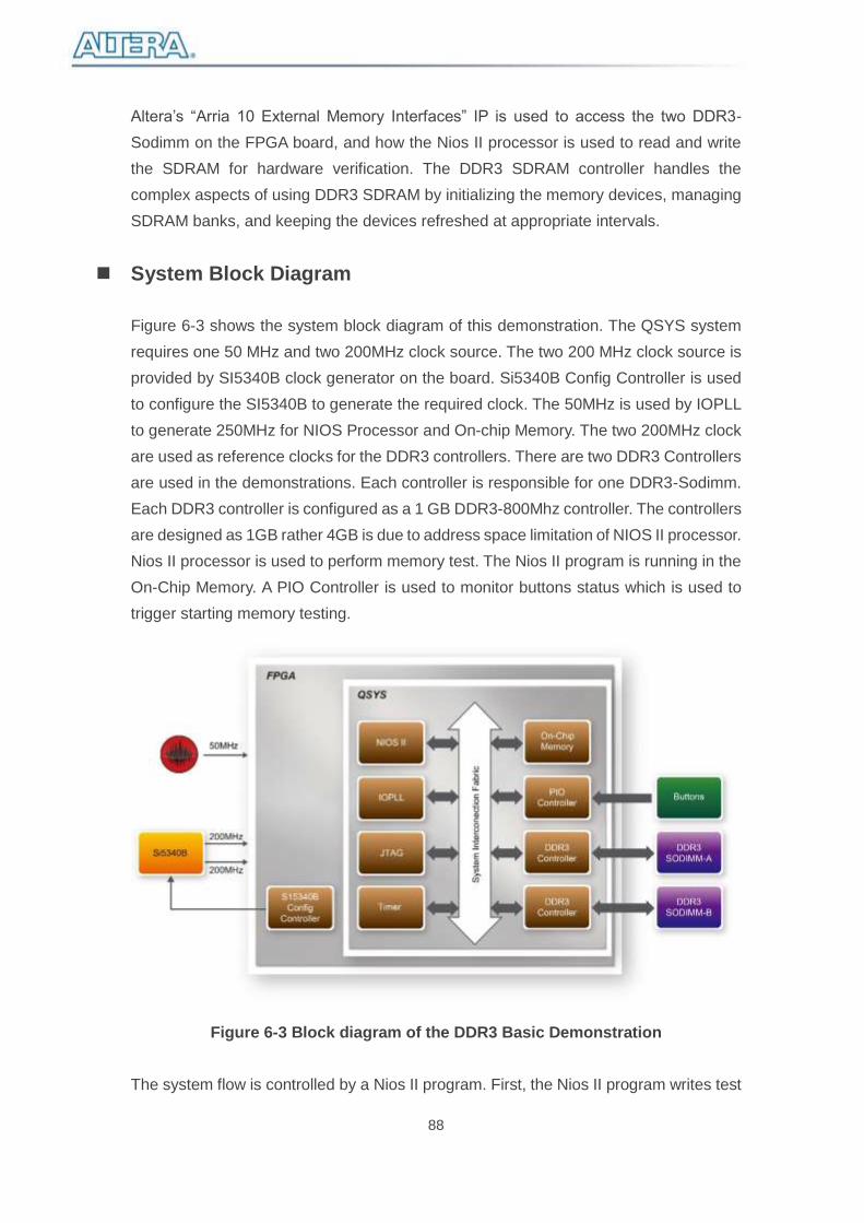
88
Altera’s “Arria 10 External Memory Interfaces” IP is used to access the two DDR3-
Sodimm on the FPGA board, and how the Nios II processor is used to read and write
the SDRAM for hardware verification. The DDR3 SDRAM controller handles the
complex aspects of using DDR3 SDRAM by initializing the memory devices, managing
SDRAM banks, and keeping the devices refreshed at appropriate intervals.
System Block Diagram
Figure 6-3 shows the system block diagram of this demonstration. The QSYS system
requires one 50 MHz and two 200MHz clock source. The two 200 MHz clock source is
provided by SI5340B clock generator on the board. Si5340B Config Controller is used
to configure the SI5340B to generate the required clock. The 50MHz is used by IOPLL
to generate 250MHz for NIOS Processor and On-chip Memory. The two 200MHz clock
are used as reference clocks for the DDR3 controllers. There are two DDR3 Controllers
are used in the demonstrations. Each controller is responsible for one DDR3-Sodimm.
Each DDR3 controller is configured as a 1 GB DDR3-800Mhz controller. The controllers
are designed as 1GB rather 4GB is due to address space limitation of NIOS II processor.
Nios II processor is used to perform memory test. The Nios II program is running in the
On-Chip Memory. A PIO Controller is used to monitor buttons status which is used to
trigger starting memory testing.
Figure 6-3 Block diagram of the DDR3 Basic Demonstration
The system flow is controlled by a Nios II program. First, the Nios II program writes test

89
patterns into the whole 1 GB of SDRAM. Then, it calls Nios II system function,
alt_dache_flush_all, to make sure all data has been written to SDRAM. Finally, it reads
data from SDRAM for data verification. The program will show progress in JTAG-
Terminal when writing/reading data to/from the SDRAM. When verification process is
completed, the result is displayed in the JTAG-Terminal.
Design Tools
Quartus II 15.1
Nios II Eclipse 15.1
Demonstration Source Code
Quartus Project directory: Nios_DDR3_X2
Nios II Eclipse: NIOS_DDR3_X2\software
Nios II Project Compilation
Nios II Project Compilation
Before you attempt to compile the reference design under Nios II Eclipse, make sure
the project is cleaned first by clicking ‘Clean’ from the ‘Project’ menu of Nios II Eclipse.
Demonstration Batch File
Demo Batch File Folder: NIOS_DDR3_X2\demo_batch
The demo batch file includes following files:
Batch File for USB-Blaseter II: test.bat, test.sh
FPGA Configure File: DE5A_NET.sof
Nios II Program: TEST_MEM.elf
Demonstration Setup
Please follow below procedures to setup the demonstartons.
Make sure Quartus II and Nios II are installed on your PC.
Make sure both DDR3 SODIMMs are installed on the FPGA board.
Power on the FPGA board.
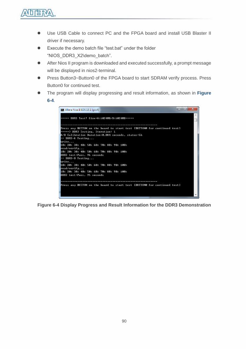
90
Use USB Cable to connect PC and the FPGA board and install USB Blaster II
driver if necessary.
Execute the demo batch file “test.bat” under the folder
“NIOS_DDR3_X2\demo_batch”.
After Nios II program is downloaded and executed successfully, a prompt message
will be displayed in nios2-terminal.
Press Button3~Button0 of the FPGA board to start SDRAM verify process. Press
Button0 for continued test.
The program will display progressing and result information, as shown in Figure
6-4.
Figure 6-4 Display Progress and Result Information for the DDR3 Demonstration

91
Chapter 7
PCI Express Reference
Design
CI Express is commonly used in consumer, server, and industrial applications,
to link motherboard-mounted peripherals. From this demonstration, it will show
how the PC and FPGA communicate with each other through the PCI Express
interface. Arria 10 Hard IP for PCI Express with Avalon-MM DMA IP is used in this
demonstration. For detail about this IP, please refer to Altera document
ug_a10_pcie_avmm_dma.pdf.
7.1 PCI Express System Infrastructure
Figure 7-1 shows the infrastructure of the PCI Express System in this demonstration.
It consists of two primary components: FPGA System and PC System. The FPGA
System is developed based on Arria 10 Hard IP for PCI Express with Avalon-MM DMA.
The application software on the PC side is developed by Terasic based on Altera’s PCIe
kernel mode driver.
P

92
Figure 7-1 Infrastructure of PCI Express System
7.2 PC PCI Express Software SDK
The FPGA System CD contains a PC Windows based SDK to allow users to develop
their 64-bit software application on Windows 7/Window XP 64-bit. The SDK is located
in the “CDROM \demonstrations\PCIe_SW_KIT” folder which includes:
PCI Express Driver
PCI Express Library
PCI Express Examples
The kernel mode driver assumes the PCIe vender ID (VID) is 0x1172 and the device ID
(DID) is 0xE003. If different VID and DID are used in the design, users need to modify
the PCIe vender ID (VID) and device ID (DID) in the driver INF file accordingly.
The PCI Express Library is implemented as a single DLL named
TERASIC_PCIE_AVMM.DLL.
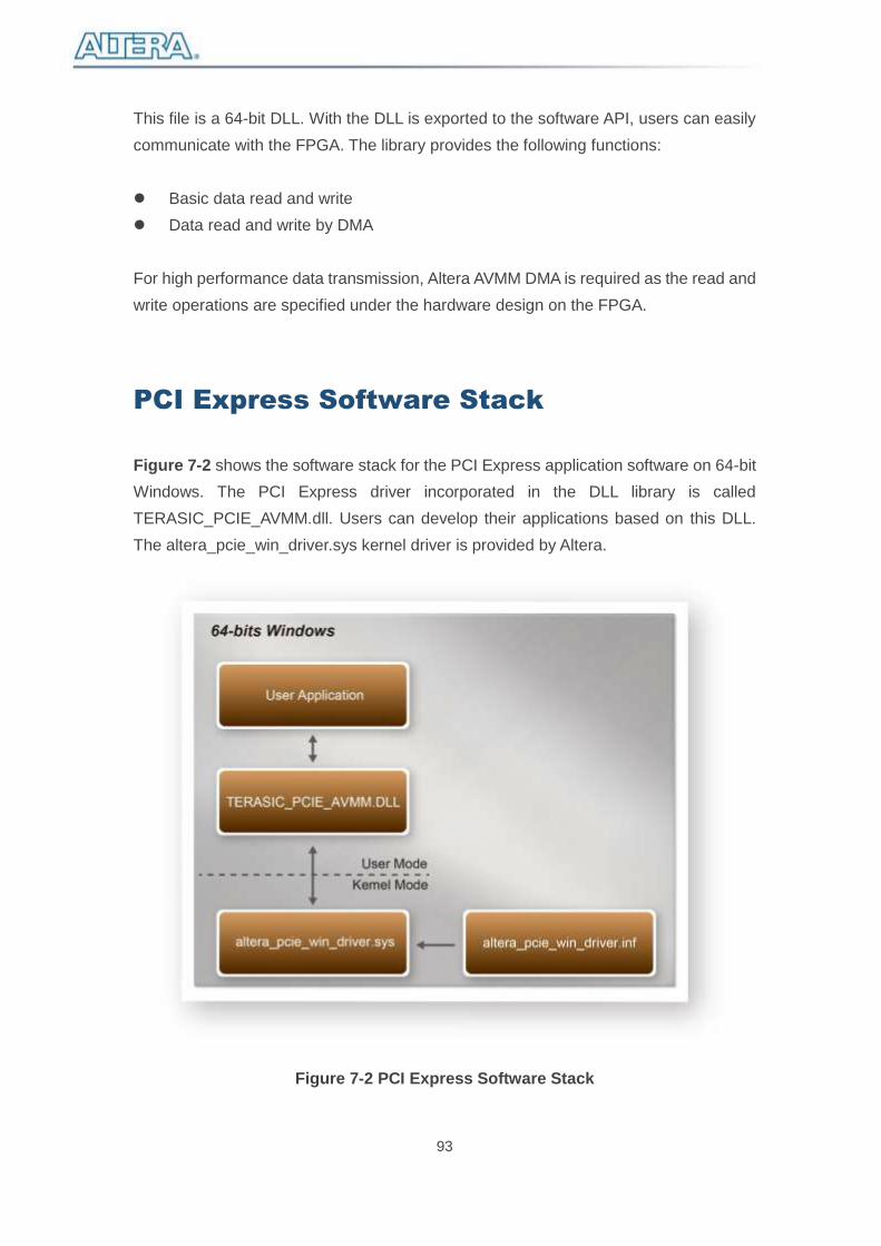
93
This file is a 64-bit DLL. With the DLL is exported to the software API, users can easily
communicate with the FPGA. The library provides the following functions:
Basic data read and write
Data read and write by DMA
For high performance data transmission, Altera AVMM DMA is required as the read and
write operations are specified under the hardware design on the FPGA.
PCI Express Software Stack
Figure 7-2 shows the software stack for the PCI Express application software on 64-bit
Windows. The PCI Express driver incorporated in the DLL library is called
TERASIC_PCIE_AVMM.dll. Users can develop their applications based on this DLL.
The altera_pcie_win_driver.sys kernel driver is provided by Altera.
Figure 7-2 PCI Express Software Stack

94
Install PCI Express Driver on Windows
The PCIe driver is locate in the folder:
“CDROM\Demonstrations\PCIe_SW_KIT\PCIe_Driver “
The folder includes the following four files:
Altera_pcie_win_driver.cat
Altera_pcie_win_driver.inf
Altera_pcie_win_driver.sys
WdfCoinstaller01011.dll
To install the PCI Express driver, please execute the steps below:
1. Install the DE5a-Net on the PCIe slot of the host PC
2. Make sure Altera Programmer and USB-Blaster II driver are installed
3. Execute test.bat in “CDROM\Demonstrations\PCIe_Fundamental\demo_batch”
to configure the FPGA
4. Restart windows operation system
5. Click Control Panel menu from Windows Start menu. Click Hardware and Sound
item before clicking the Device Manager to launch the Device Manager dialog.
There will be a PCI Device item in the dialog, as shown in Figure 7-3. Move the
mouse cursor to the PCI Device item and right click it to select the Update Driver
Software... item.
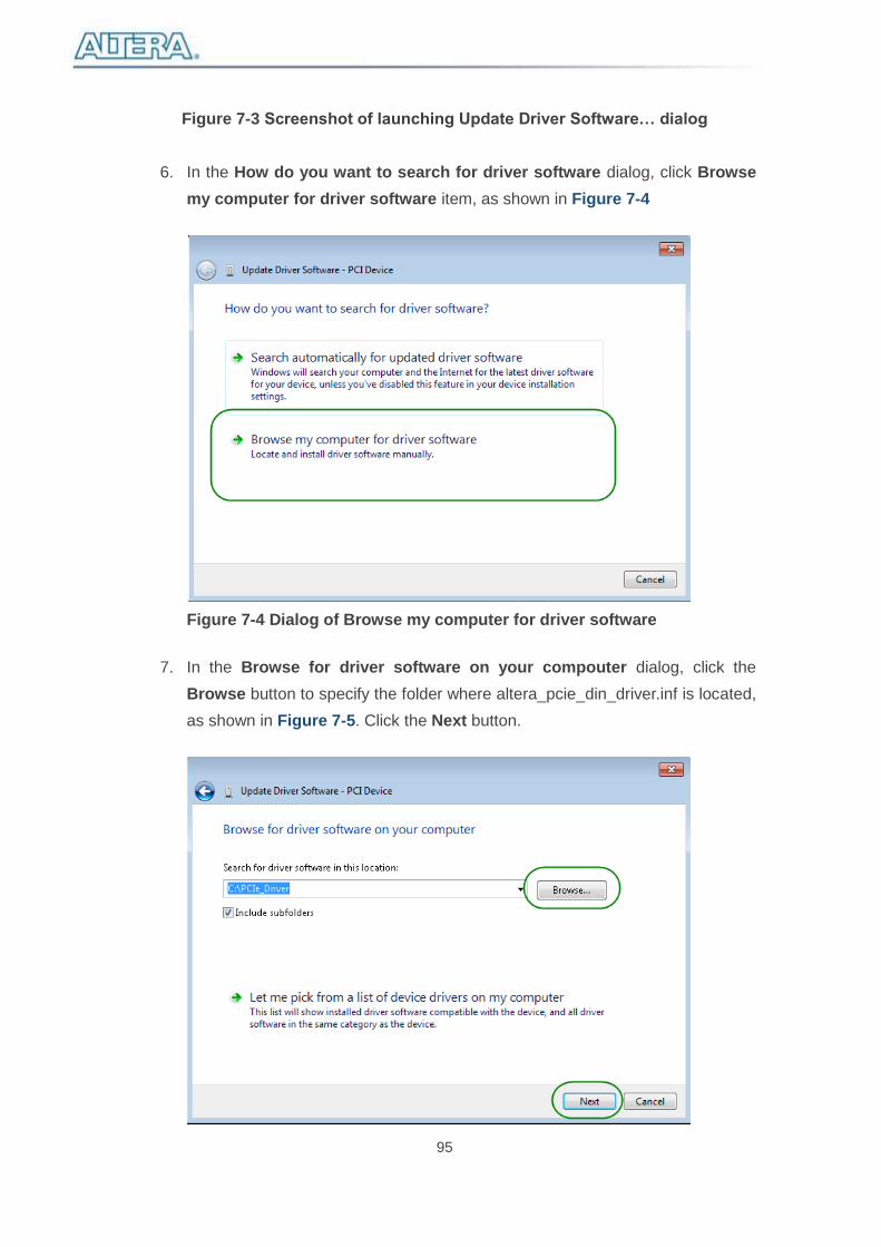
95
Figure 7-3 Screenshot of launching Update Driver Software… dialog
6. In the How do you want to search for driver software dialog, click Browse
my computer for driver software item, as shown in Figure 7-4
Figure 7-4 Dialog of Browse my computer for driver software
7. In the Browse for driver software on your compouter dialog, click the
Browse button to specify the folder where altera_pcie_din_driver.inf is located,
as shown in Figure 7-5. Click the Next button.

96
Figure 7-5 Browse for driver software on your computer
8. When the Windows Security dialog appears, as shown Figure 7-5, click the
Install button.
Figure 7-6 Click Install in the dialog of Windows Security
9. When the driver is installed successfully, the successfully dialog will appears, as
shown in Figure 7-7. Click the Close button.
Figure 7-7 Click Close when the installation of Altera PCI API Driver is
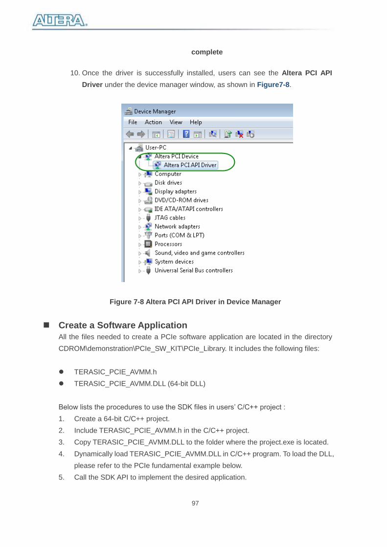
97
complete
10. Once the driver is successfully installed, users can see the Altera PCI API
Driver under the device manager window, as shown in Figure7-8.
Figure 7-8 Altera PCI API Driver in Device Manager
Create a Software Application
All the files needed to create a PCIe software application are located in the directory
CDROM\demonstration\PCIe_SW_KIT\PCIe_Library. It includes the following files:
TERASIC_PCIE_AVMM.h
TERASIC_PCIE_AVMM.DLL (64-bit DLL)
Below lists the procedures to use the SDK files in users’ C/C++ project :
1. Create a 64-bit C/C++ project.
2. Include TERASIC_PCIE_AVMM.h in the C/C++ project.
3. Copy TERASIC_PCIE_AVMM.DLL to the folder where the project.exe is located.
4. Dynamically load TERASIC_PCIE_AVMM.DLL in C/C++ program. To load the DLL,
please refer to the PCIe fundamental example below.
5. Call the SDK API to implement the desired application.
98
Users can easily communicate with the FPGA through the PCIe bus through the
TERASIC_PCIE_AVMM.DLL API. The details of API are described below:
PCIE_Open
Function:
Open a specified PCIe card with vendor ID, device ID, and matched card index.
Prototype:
PCIE_HANDLE PCIE_Open(
WORD wVendorID,
WORD wDeviceID,
WORD wCardIndex);
Parameters:
wVendorID:
Specify the desired vendor ID. A zero value means to ignore the vendor ID.
wDeviceID:
Specify the desired device ID. A zero value means to ignore the device ID.
wCardIndex:
Specify the matched card index, a zero based index, based on the matched verder
ID and device ID.
Return Value:
Return a handle to presents specified PCIe card. A positive value is return if the PCIe
card is opened successfully. A value zero means failed to connect the target PCIe
card.
This handle value is used as a parameter for other functions, e.g. PCIE_Read32.
Users need to call PCIE_Close to release handle once the handle is no more used.
PCIE_Close
Function:
Close a handle associated to the PCIe card.
Prototype:
void PCIE_Close(
PCIE_HANDLE hPCIE);
Parameters:
hPCIE: A PCIe handle return by PCIE_Open function.
Return Value:
None.
PCIE_Read32
99
Function:
Read a 32-bit data from the FPGA board.
Prototype:
bool PCIE_Read32(
PCIE_HANDLE hPCIE,
PCIE_BAR PcieBar,
PCIE_ADDRESS PcieAddress,
DWORD * pdwData);
Parameters:
hPCIE:
A PCIe handle return by PCIE_Open function.
PcieBar:
Specify the target BAR.
PcieAddress:
Specify the target address in FPGA.
pdwData:
A buffer to retrieve the 32-bit data.
Return Value:
Return TRUE if read data is successful; otherwise FALSE is returned.
PCIE_Write32
Function:
Write a 32-bit data to the FPGA Board.
Prototype:
bool PCIE_Write32(
PCIE_HANDLE hPCIE,
PCIE_BAR PcieBar,
PCIE_ADDRESS PcieAddress,
DWORD dwData);
Parameters:
hPCIE:
A PCIe handle return by PCIE_Open function.
PcieBar:
Specify the target BAR.
PcieAddress:
Specify the target address in FPGA.
dwData:
Specify a 32-bit data which will be written to FPGA board.
100
Return Value:
Return TRUE if write data is successful; otherwise FALSE is returned.
PCIE_DmaRead
Function:
Read data from the memory-mapped memory of FPGA board in DMA.
Prototype:
bool PCIE_DmaRead(
PCIE_HANDLE hPCIE,
PCIE_LOCAL_ADDRESS LocalAddress,
void *pBuffer,
DWORD dwBufSize
);
Parameters:
hPCIE:
A PCIe handle return by PCIE_Open function.
LocalAddress:
Specify the target memory-mapped address in FPGA.
pBuffer:
A pointer to a memory buffer to retrieved the data from FPGA. The size of buffer
should be equal or larger the dwBufSize.
dwBufSize:
Specify the byte number of data retrieved from FPGA.
Return Value:
Return TRUE if read data is successful; otherwise FALSE is returned.
PCIE_DmaWrite
Function:
Write data to the memory-mapped memory of FPGA board in DMA.
Prototype:
bool PCIE_DmaWrite(
PCIE_HANDLE hPCIE,
PCIE_LOCAL_ADDRESS LocalAddress,
void *pData,
DWORD dwDataSize
);
Parameters:
hPCIE:
101
A PCIe handle return by PCIE_Open function.
LocalAddress:
Specify the target memory mapped address in FPGA.
pData:
A pointer to a memory buffer to store the data which will be written to FPGA.
dwDataSize:
Specify the byte number of data which will be written to FPGA.
Return Value:
Return TRUE if write data is successful; otherwise FALSE is returned.
PCIE_ConfigRead32
Function:
Read PCIe Configuration Table. Read a 32-bit data by given a byte offset.
Prototype:
bool PCIE_ConfigRead32 (
PCIE_HANDLE hPCIE,
DWORD Offset,
DWORD *pdwData
);
Parameters:
hPCIE:
A PCIe handle return by PCIE_Open function.
Offset:
Specify the target byte of offset in PCIe configuration table.
pdwData:
A 4-bytes buffer to retrieve the 32-bit data.
Return Value:
Return TRUE if read data is successful; otherwise FALSE is returned.
7.3 PCIe Reference Design - Fundamental
The application reference design shows how to implement fundamental control and data
transfer in DMA. In the design, basic I/O is used to control the BUTTON and LED on
the FPGA board. High-speed data transfer is performed by DMA.
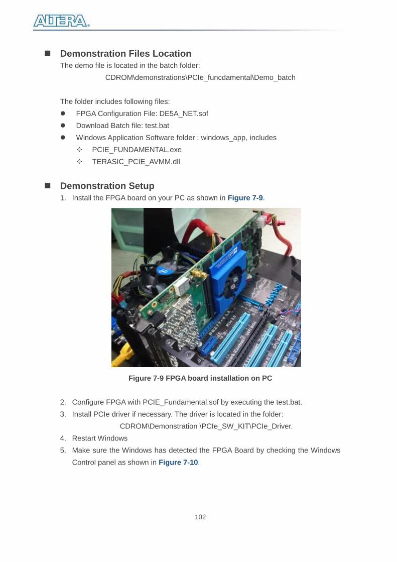
102
Demonstration Files Location
The demo file is located in the batch folder:
CDROM\demonstrations\PCIe_funcdamental\Demo_batch
The folder includes following files:
FPGA Configuration File: DE5A_NET.sof
Download Batch file: test.bat
Windows Application Software folder : windows_app, includes
PCIE_FUNDAMENTAL.exe
TERASIC_PCIE_AVMM.dll
Demonstration Setup
1. Install the FPGA board on your PC as shown in Figure 7-9.
Figure 7-9 FPGA board installation on PC
2. Configure FPGA with PCIE_Fundamental.sof by executing the test.bat.
3. Install PCIe driver if necessary. The driver is located in the folder:
CDROM\Demonstration \PCIe_SW_KIT\PCIe_Driver.
4. Restart Windows
5. Make sure the Windows has detected the FPGA Board by checking the Windows
Control panel as shown in Figure 7-10.
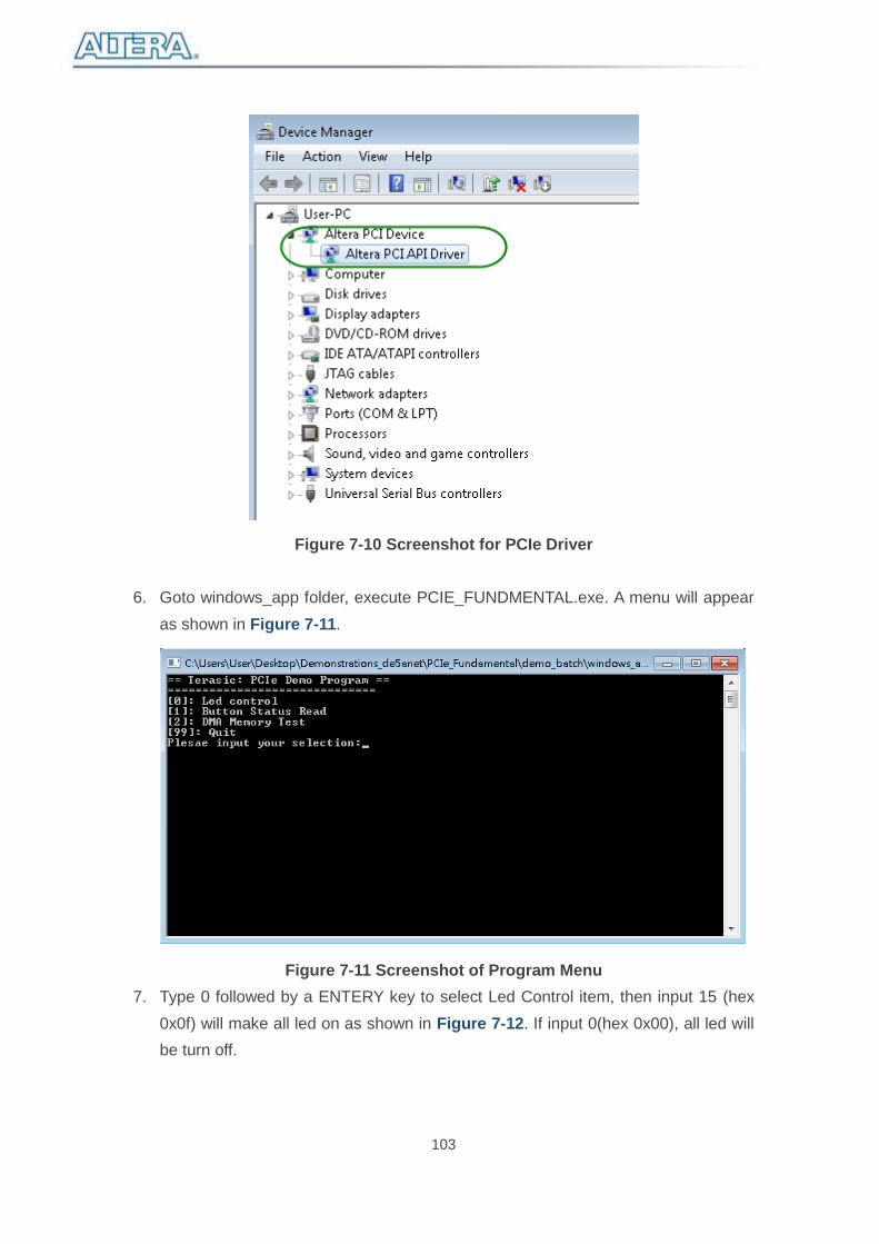
103
Figure 7-10 Screenshot for PCIe Driver
6. Goto windows_app folder, execute PCIE_FUNDMENTAL.exe. A menu will appear
as shown in Figure 7-11.
Figure 7-11 Screenshot of Program Menu
7. Type 0 followed by a ENTERY key to select Led Control item, then input 15 (hex
0x0f) will make all led on as shown in Figure 7-12. If input 0(hex 0x00), all led will
be turn off.
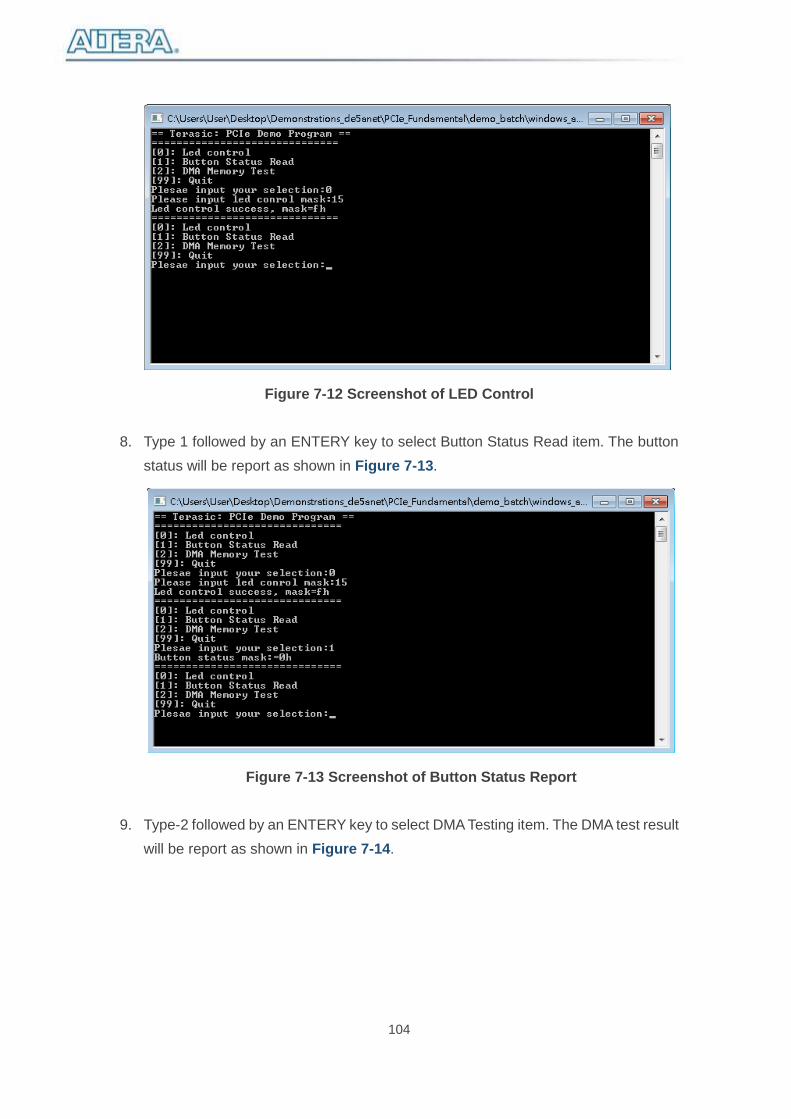
104
Figure 7-12 Screenshot of LED Control
8. Type 1 followed by an ENTERY key to select Button Status Read item. The button
status will be report as shown in Figure 7-13.
Figure 7-13 Screenshot of Button Status Report
9. Type-2 followed by an ENTERY key to select DMA Testing item. The DMA test result
will be report as shown in Figure 7-14.
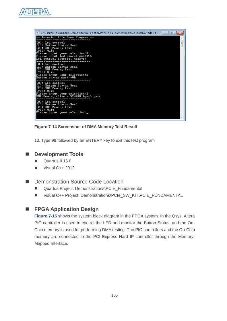
105
Figure 7-14 Screenshot of DMA Memory Test Result
10. Type 99 followed by an ENTERY key to exit this test program
Development Tools
Quartus II 16.0
Visual C++ 2012
Demonstration Source Code Location
Quartus Project: Demonstrations\PCIE_Fundamental
Visual C++ Project: Demonstrations\PCIe_SW_KIT\PCIE_FUNDAMENTAL
FPGA Application Design
Figure 7-15 shows the system block diagram in the FPGA system. In the Qsys, Altera
PIO controller is used to control the LED and monitor the Button Status, and the On-
Chip memory is used for performing DMA testing. The PIO controllers and the On-Chip
memory are connected to the PCI Express Hard IP controller through the Memory-
Mapped Interface.
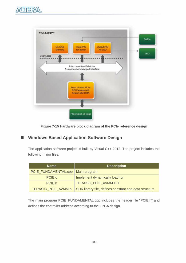
106
Figure 7-15 Hardware block diagram of the PCIe reference design
Windows Based Application Software Design
The application software project is built by Visual C++ 2012. The project includes the
following major files:
Name Description
PCIE_FUNDAMENTAL.cpp Main program
PCIE.c Implement dynamically load for
TERAISC_PCIE_AVMM.DLL PCIE.h
TERASIC_PCIE_AVMM.h SDK library file, defines constant and data structure
The main program PCIE_FUNDAMENTAL.cpp includes the header file "PCIE.h" and
defines the controller address according to the FPGA design.
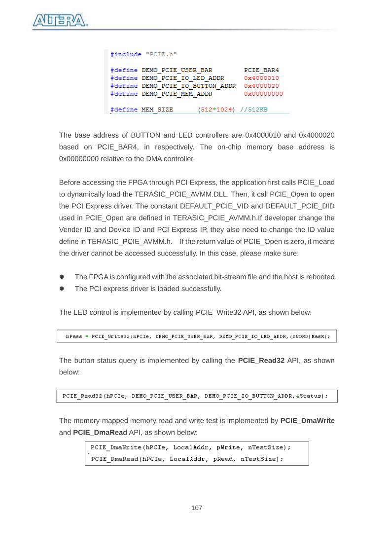
107
The base address of BUTTON and LED controllers are 0x4000010 and 0x4000020
based on PCIE_BAR4, in respectively. The on-chip memory base address is
0x00000000 relative to the DMA controller.
Before accessing the FPGA through PCI Express, the application first calls PCIE_Load
to dynamically load the TERASIC_PCIE_AVMM.DLL. Then, it call PCIE_Open to open
the PCI Express driver. The constant DEFAULT_PCIE_VID and DEFAULT_PCIE_DID
used in PCIE_Open are defined in TERASIC_PCIE_AVMM.h.If developer change the
Vender ID and Device ID and PCI Express IP, they also need to change the ID value
define in TERASIC_PCIE_AVMM.h. If the return value of PCIE_Open is zero, it means
the driver cannot be accessed successfully. In this case, please make sure:
The FPGA is configured with the associated bit-stream file and the host is rebooted.
The PCI express driver is loaded successfully.
The LED control is implemented by calling PCIE_Write32 API, as shown below:
The button status query is implemented by calling the PCIE_Read32 API, as shown
below:
The memory-mapped memory read and write test is implemented by PCIE_DmaWrite
and PCIE_DmaRead API, as shown below:
108
7.4 PCIe Reference Design – DDR3
The application reference design shows how to add DDR3 Memory Controllers for
DDR3-A SODIMM and DDR3-B SODIMM into the PCIe Quartus project based on the
PCI_Fundamental Quartus project and perform 2GB data DMA for both SODIMM. Also,
this demo shows how to call “PCIE_ConfigRead32” API to check PCIe link status.
Demonstration Files Location
The demo file is located in the batch folder:
CDROM\demonstrations\PCIe_DDR3\Demo_batch
The folder includes following files:
FPGA Configuration File: DE5A_NET.sof
Download Batch file: test.bat
Windows Application Software folder : windows_app, includes
PCIE_DDR3.exe
TERASIC_PCIE_AVMM.dll
Demonstration Setup
1. Install both DDR3 2133 4GB SODIMM on the FPGA board.
2. Install the FPGA board on your PC.
3. Configure FPGA with PCIE_DDR3.sof by executing the test.bat.
4. Install PCIe driver if necessary.
5. Restart Windows
6. Make sure the Windows has detected the FPGA Board by checking the Windows
Control panel.
7. Goto windows_app folder, execute PCIE_DDR3.exe. A menu will appear as shown
in Figure 7-16.
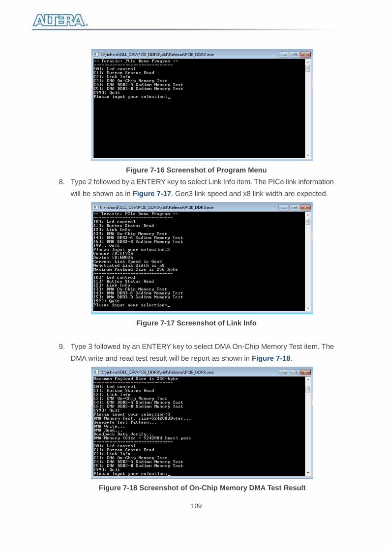
109
Figure 7-16 Screenshot of Program Menu
8. Type 2 followed by a ENTERY key to select Link Info item. The PICe link information
will be shown as in Figure 7-17. Gen3 link speed and x8 link width are expected.
Figure 7-17 Screenshot of Link Info
9. Type 3 followed by an ENTERY key to select DMA On-Chip Memory Test item. The
DMA write and read test result will be report as shown in Figure 7-18.
Figure 7-18 Screenshot of On-Chip Memory DMA Test Result
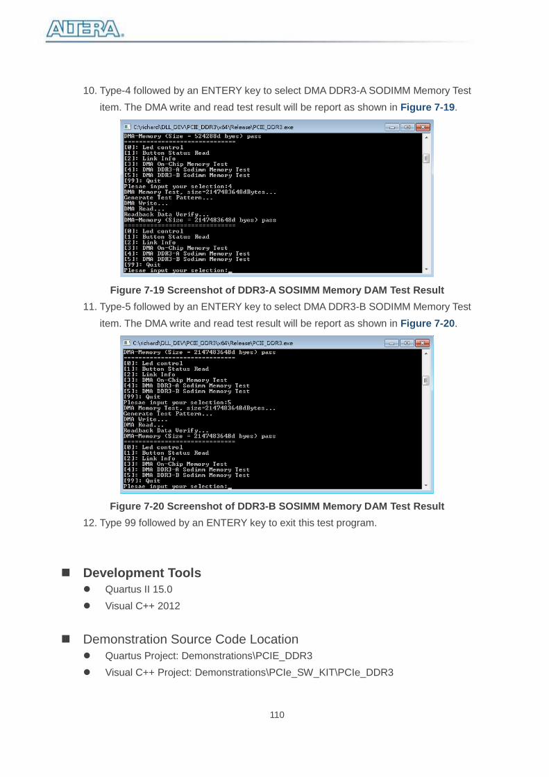
110
10. Type-4 followed by an ENTERY key to select DMA DDR3-A SODIMM Memory Test
item. The DMA write and read test result will be report as shown in Figure 7-19.
Figure 7-19 Screenshot of DDR3-A SOSIMM Memory DAM Test Result
11. Type-5 followed by an ENTERY key to select DMA DDR3-B SODIMM Memory Test
item. The DMA write and read test result will be report as shown in Figure 7-20.
Figure 7-20 Screenshot of DDR3-B SOSIMM Memory DAM Test Result
12. Type 99 followed by an ENTERY key to exit this test program.
Development Tools
Quartus II 15.0
Visual C++ 2012
Demonstration Source Code Location
Quartus Project: Demonstrations\PCIE_DDR3
Visual C++ Project: Demonstrations\PCIe_SW_KIT\PCIe_DDR3
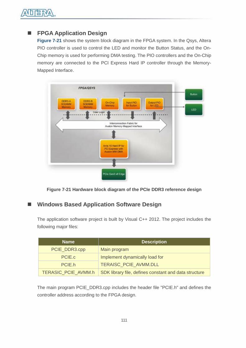
111
FPGA Application Design
Figure 7-21 shows the system block diagram in the FPGA system. In the Qsys, Altera
PIO controller is used to control the LED and monitor the Button Status, and the On-
Chip memory is used for performing DMA testing. The PIO controllers and the On-Chip
memory are connected to the PCI Express Hard IP controller through the Memory-
Mapped Interface.
Figure 7-21 Hardware block diagram of the PCIe DDR3 reference design
Windows Based Application Software Design
The application software project is built by Visual C++ 2012. The project includes the
following major files:
Name Description
PCIE_DDR3.cpp Main program
PCIE.c Implement dynamically load for
TERAISC_PCIE_AVMM.DLL PCIE.h
TERASIC_PCIE_AVMM.h SDK library file, defines constant and data structure
The main program PCIE_DDR3.cpp includes the header file "PCIE.h" and defines the
controller address according to the FPGA design.
112
The base address of BUTTON and LED controllers are 0x4000010 and 0x4000020
based on PCIE_BAR4, in respectively. The on-chip memory base address is
0x00000000 relative to the DMA controller. The above definition is the same as those
in PCIe Fundamental demo.
Before accessing the FPGA through PCI Express, the application first calls PCIE_Load
to dynamically load the TERASIC_PCIE_AVMM.DLL. Then, it call PCIE_Open to open
the PCI Express driver. The constant DEFAULT_PCIE_VID and DEFAULT_PCIE_DID
used in PCIE_Open are defined in TERASIC_PCIE_AVMM.h.If developer change the
Vender ID and Device ID and PCI Express IP, they also need to change the ID value
define in TERASIC_PCIE_AVMM.h. If the return value of PCIE_Open is zero, it means
the driver cannot be accessed successfully. In this case, please make sure:
The FPGA is configured with the associated bit-stream file and the host is rebooted.
The PCI express driver is loaded successfully.
The LED control is implemented by calling PCIE_Write32 API, as shown below:
The button status query is implemented by calling the PCIE_Read32 API, as shown
below:
The memory-mapped memory read and write test is implemented by PCIE_DmaWrite
and PCIE_DmaRead API, as shown below:
113
The pcie link information is implemented by PCIE_ConfigRead32 API, as shown below:
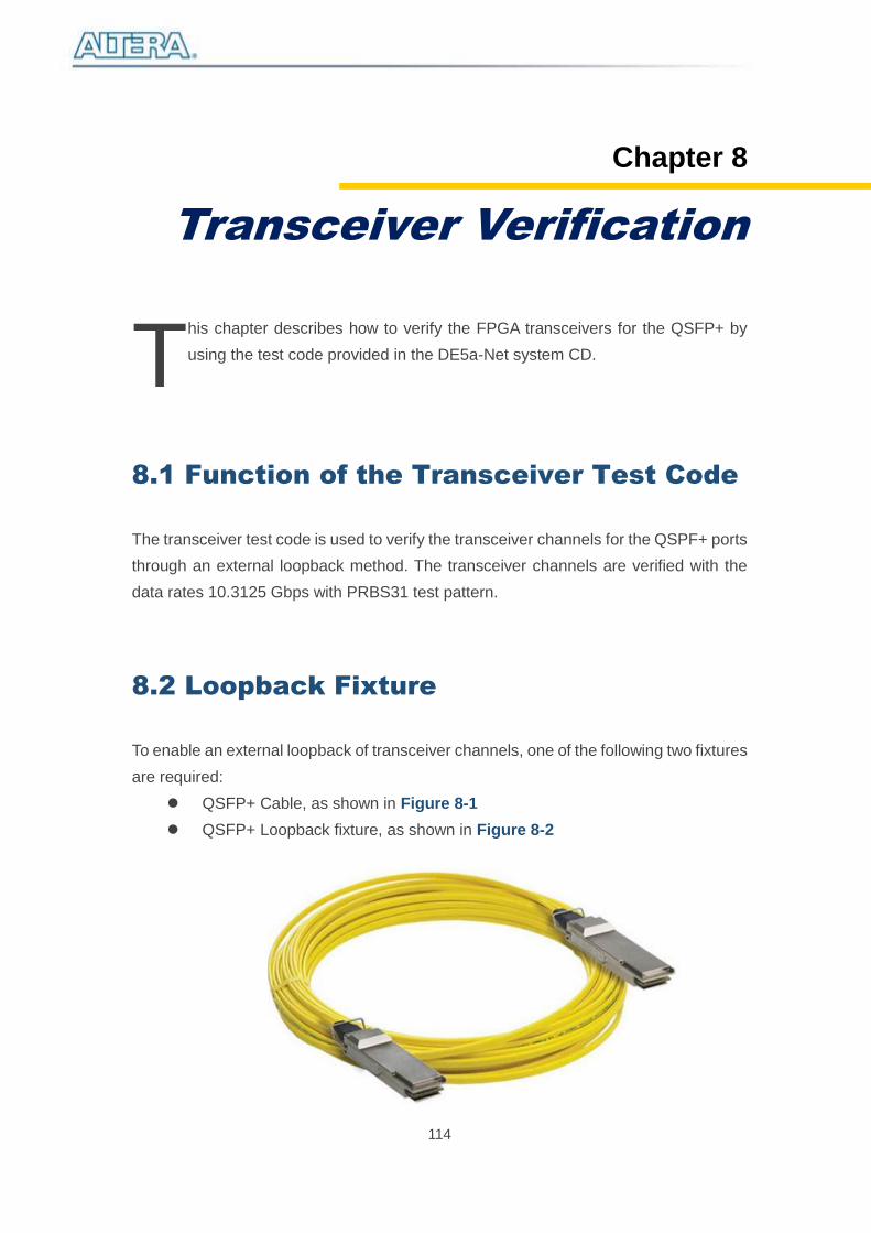
114
Chapter 8
Transceiver Verification
his chapter describes how to verify the FPGA transceivers for the QSFP+ by
using the test code provided in the DE5a-Net system CD.
8.1 Function of the Transceiver Test Code
The transceiver test code is used to verify the transceiver channels for the QSPF+ ports
through an external loopback method. The transceiver channels are verified with the
data rates 10.3125 Gbps with PRBS31 test pattern.
8.2 Loopback Fixture
To enable an external loopback of transceiver channels, one of the following two fixtures
are required:
QSFP+ Cable, as shown in Figure 8-1
QSFP+ Loopback fixture, as shown in Figure 8-2
T
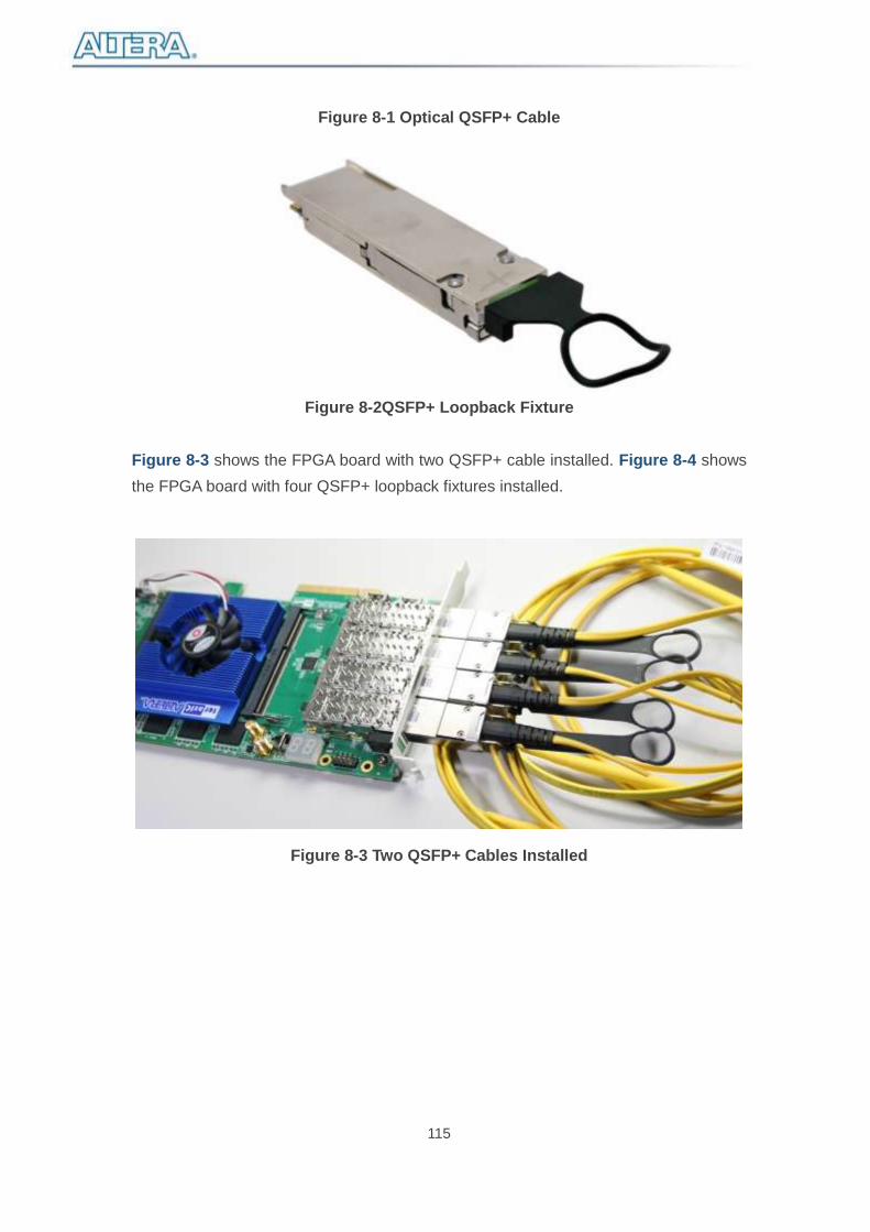
115
Figure 8-1 Optical QSFP+ Cable
Figure 8-2QSFP+ Loopback Fixture
Figure 8-3 shows the FPGA board with two QSFP+ cable installed. Figure 8-4 shows
the FPGA board with four QSFP+ loopback fixtures installed.
Figure 8-3 Two QSFP+ Cables Installed
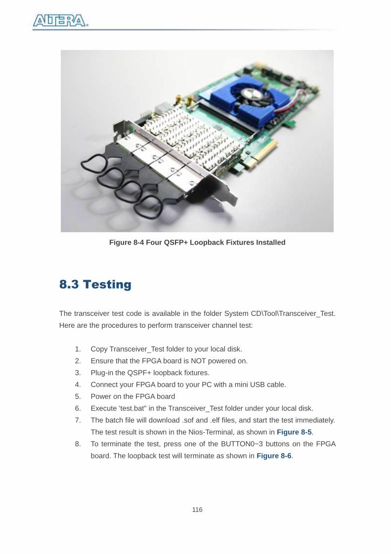
116
Figure 8-4 Four QSFP+ Loopback Fixtures Installed
8.3 Testing
The transceiver test code is available in the folder System CD\Tool\Transceiver_Test.
Here are the procedures to perform transceiver channel test:
1. Copy Transceiver_Test folder to your local disk.
2. Ensure that the FPGA board is NOT powered on.
3. Plug-in the QSPF+ loopback fixtures.
4. Connect your FPGA board to your PC with a mini USB cable.
5. Power on the FPGA board
6. Execute 'test.bat" in the Transceiver_Test folder under your local disk.
7. The batch file will download .sof and .elf files, and start the test immediately.
The test result is shown in the Nios-Terminal, as shown in Figure 8-5.
8. To terminate the test, press one of the BUTTON0~3 buttons on the FPGA
board. The loopback test will terminate as shown in Figure 8-6.
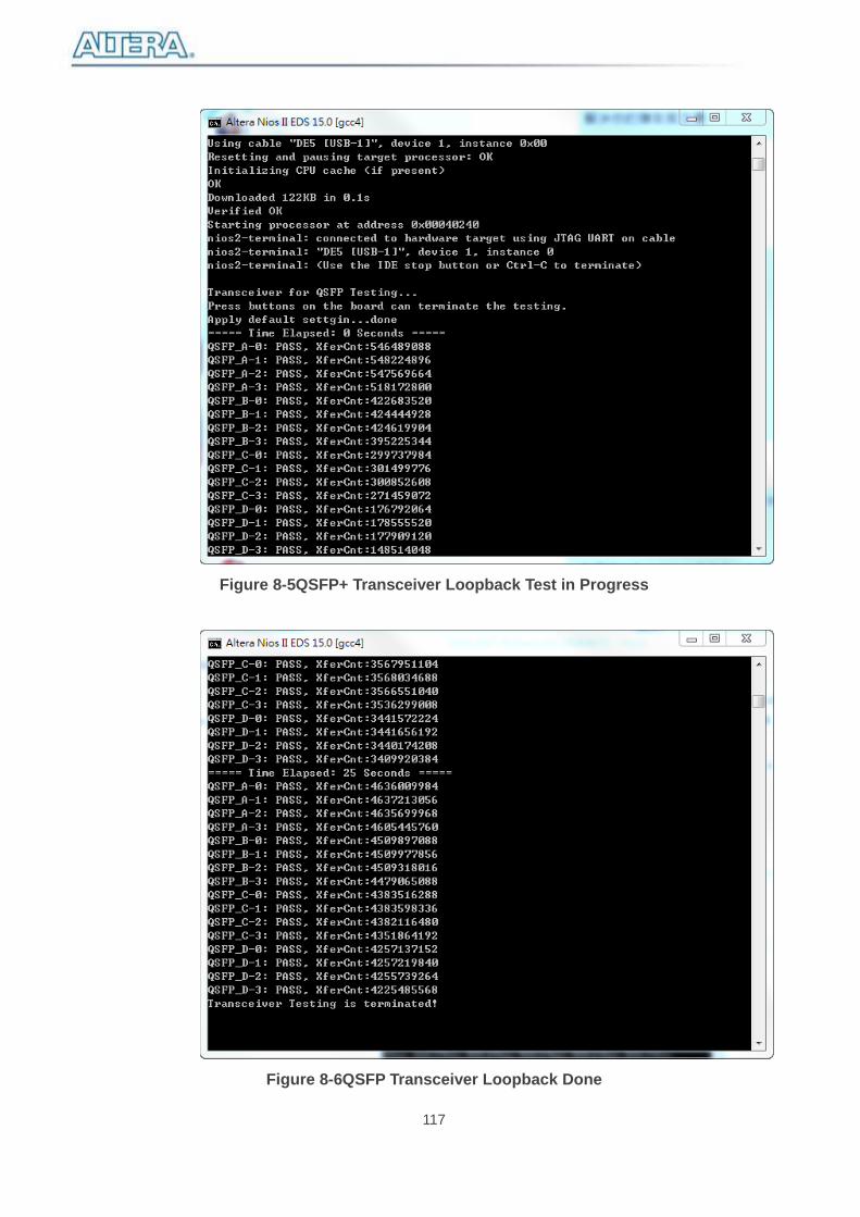
117
Figure 8-5QSFP+ Transceiver Loopback Test in Progress
Figure 8-6QSFP Transceiver Loopback Done
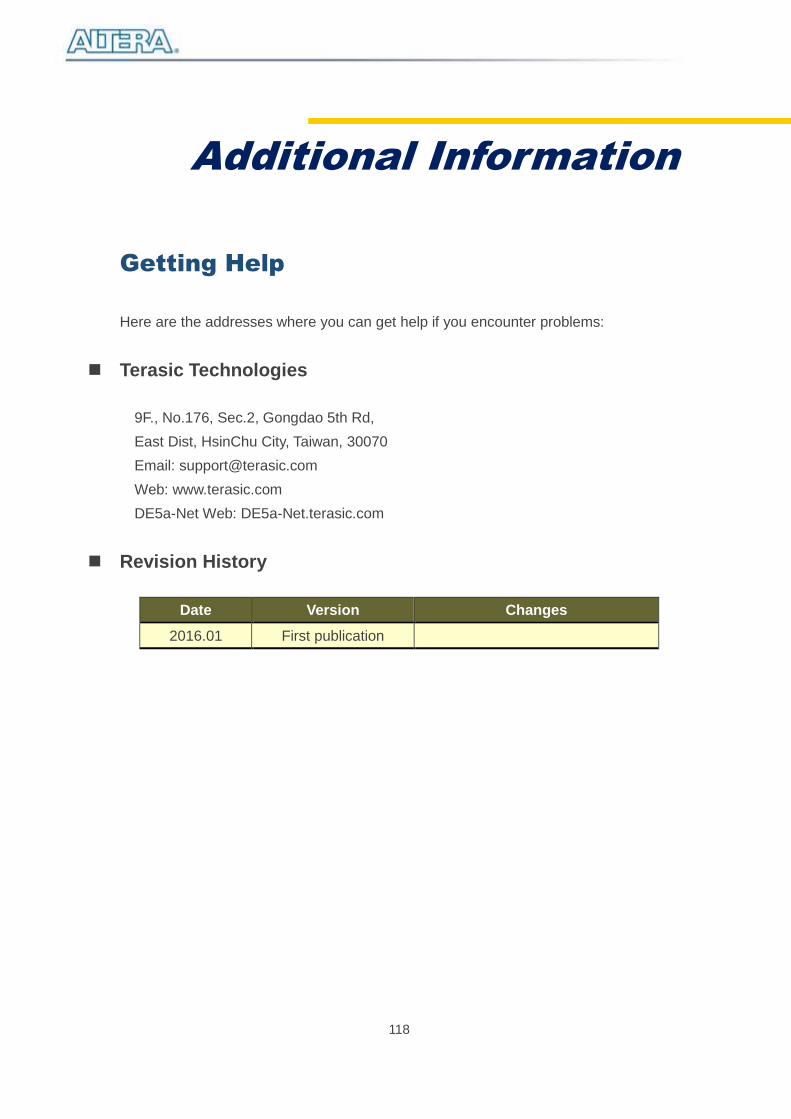
118
Additional Information
Getting Help
Here are the addresses where you can get help if you encounter problems:
Terasic Technologies
9F., No.176, Sec.2, Gongdao 5th Rd,
East Dist, HsinChu City, Taiwan, 30070
Email: [email protected]
Web: www.terasic.com
DE5a-Net Web: DE5a-Net.terasic.com
Revision History
Date Version Changes
2016.01 First publication


