11 Chapter 1 INTRODUCTION General Introduction to nanomaterials, their methods of preparation, properties and applications are described in this Chapter. Aim of the present work and Chapter-wise break-up of the thesis are also included in it. 1.1 Introduction to nanomaterials Literature reveals that the history of nanomaterials bEgan immediately after the big bang when nanostructures were formed in the early meteorites [1]. Nature later evolved many other nanostructures like seashells, skeletons etc. Nano scaled smoke materials were formed during the use of fire by early humans. However, the scientific story of nanomaterials bEgan much later. One of the first scientific reports is the colloidal gold nanomaterials synthesized by Michael Faraday as early as 1857 [2]. By the early 1940’s, precipitated and fumed silica nanoparticles were being manufactured and sold in USA and Germany as substitutes for ultrafine carbon black for rubber reinforcements. On Dec. 29, 1959 at the California Institute of Technology, Pasadena, Nobel Laureate Richard P. Feynman gave a talk at the annual meeting of the American Physical Society that has become one of the twentieth century’s classic science lectures, titled “There’s Plenty of Room at the Bottom” [3]. He pointed out that if a bit of information requires only 100 atoms, then all the books ever written could be stored in a cube with sides 0.02 inch long [4]. The history of nanomaterials is quite long; nevertheless, major developments with in nanoscience have taken place during the last decade or so. Research in nanomaterials is a multidisciplinary effort that involves interaction between researchers in the field of physics, chemistry, mechanics, materials science and even biology and medicine. Reportedly, the first nanoparticles based technology, which is a heterogeneous catalyst, was developed in the early nineteenth century, followed by the use of silver halide nanoparticles in photography [5]. The discovery of novel materials, processes and phenomena at the nanoscale as well as the development of new experimental and theoretical techniques for research provide fresh opportunities for the development of innovative nanosystems and nanostructured materials. Nanosystems are expected to find various unique applications. Nanostructured materials can be made with unique materials on the basis of their properties.
Transcript
11
Chapter 1
INTRODUCTION
General Introduction to nanomaterials, their methods of preparation, properties and
applications are described in this Chapter. Aim of the present work and Chapter-wise
break-up of the thesis are also included in it.
1.1 Introduction to nanomaterialsLiterature reveals that the history of nanomaterials bEgan immediately after the big
bang when nanostructures were formed in the early meteorites [1]. Nature later evolved
many other nanostructures like seashells, skeletons etc. Nano scaled smoke materials were
formed during the use of fire by early humans. However, the scientific story of
nanomaterials bEgan much later. One of the first scientific reports is the colloidal gold
nanomaterials synthesized by Michael Faraday as early as 1857 [2]. By the early 1940’s,
precipitated and fumed silica nanoparticles were being manufactured and sold in USA and
Germany as substitutes for ultrafine carbon black for rubber reinforcements. On Dec. 29,
1959 at the California Institute of Technology, Pasadena, Nobel Laureate Richard P.
Feynman gave a talk at the annual meeting of the American Physical Society that has
become one of the twentieth century’s classic science lectures, titled “There’s Plenty of
Room at the Bottom” [3]. He pointed out that if a bit of information requires only 100
atoms, then all the books ever written could be stored in a cube with sides 0.02 inch long
[4]. The history of nanomaterials is quite long; nevertheless, major developments with in
nanoscience have taken place during the last decade or so. Research in nanomaterials is a
multidisciplinary effort that involves interaction between researchers in the field of
physics, chemistry, mechanics, materials science and even biology and medicine.
Reportedly, the first nanoparticles based technology, which is a heterogeneous catalyst,
was developed in the early nineteenth century, followed by the use of silver halide
nanoparticles in photography [5].
The discovery of novel materials, processes and phenomena at the nanoscale as well
as the development of new experimental and theoretical techniques for research provide
fresh opportunities for the development of innovative nanosystems and nanostructured
materials. Nanosystems are expected to find various unique applications. Nanostructured
materials can be made with unique materials on the basis of their properties.
12
The nanotechnology field in addition to the fabrication of nano-system provides the
platform to the development of better experimental and computational tools. Due to the
unique properties, the nanomaterials are used in industrial, commercial and defence
applications. Micro-and nanosystems are likely to be the next step in the “silicon
revolution".
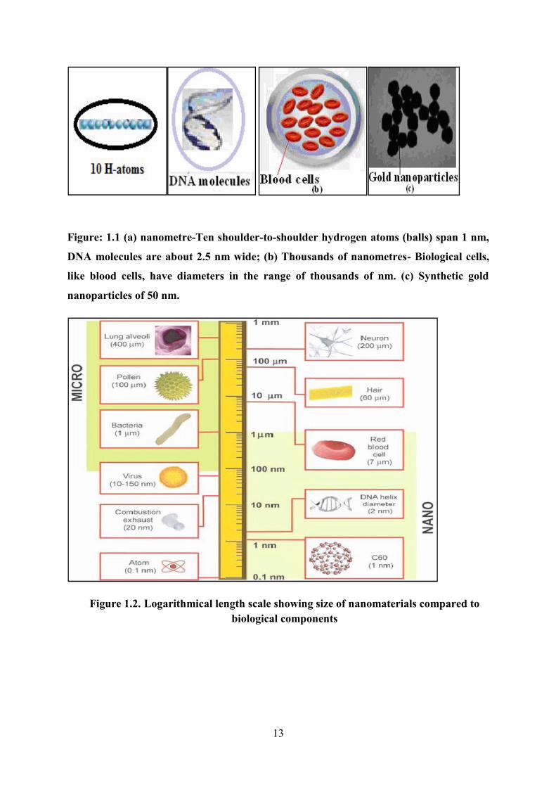
1.2 The Word “nano”The word “Nano” means dwarf in Greek language. Normally nano is used as a prefix
for any unit like a second or a metre and it means a billionth part (10-9) of that unit. A
nanosecond is one billionth of a second and a nanometre is one billionth of a metre-about
the length of a few atoms lined up shoulder to shoulder. A world of things is built up from
the tiny scale of nanometres. In contemporary science, we consider atom as the smallest
particle and nanomaterials as the smallest building blocks of the nature. Nanometre is only
1 to 5 atoms wide while nanoparticles range from 1 to 100 nm. A hydrogen atom is 0.1
nm. We frequently quote hair as the thinnest. However nanometre is about 40,000 to
80,000 times smaller than the hair. While studying biology one talks of DNA, virus,
proteins, bacteria and cells as the smallest building blocks of a body. Width of DNA is
about 2 nm.; the size of proteins range from 5 to 50 nm; virus ranges from 75 to 100 nm;
bacteria is 1000 nm, red cells are approximately 7000 nm in diameter and 2000 nm in
height while white blood cells are approximately 10,000 nm in diameter. DNA, virus,
proteins, bacteria and cells are the natures tiniest and the most wonderful machines at
micro level or nano level. If one goes deep in to the functioning of proteins, DNA,
membranes and other nanoscale devices of the nature and copies these to build scientific
devices at nanoscale, one may find very encouraging results. Examples are fullerenes of
1nm, quantum dots of 8 nm and dendrimers of about 10 nm which have revolutionary
developments in the fields of materials science, electronics, biotechnology, medicine etc.
Cellular proteins and enzymes are one of the important constituents of human body. A few
Figure 1.3 Classification of nanomaterials (a) Zero dimensional spheres and clusters,
(b) One dimensional nano-fiber, wires, and rods, (c) Two dimensional films, plates, and
networks, (d) Three dimensional materials (bulk materials).
Nanostructured materials can be created with various modulation dimensionalities
such as zero (e.g. atomic clusters, quantum dots and cluster assemblies), one (e.g.
multilayers), two (e.g. ultrafine-grained over layers or buried layers/ nanotube), and three
dimensional materials (e.g. bulk materials). Oswald was the first to realize that materials of
such dimensions should display novel and interesting properties, which have largely
dependent on their size and shape [6]. However, it is only from the last two decades that
significant interest has been devoted to inorganic materials consisting of a few hundred or
a few dozen atoms called clusters. The interest has been extended to a large variety of
metals and semiconductors because nanomaterials exhibited special properties, which
differ from corresponding macro-crystalline material. The bulk materials that are
constituted of atoms and molecules as such has been widely classified and satisfactorily
explained. On the basis of dimensionality , composition and shape nanomaterials are
classified in different categories which are described below.
15
1.3.1 One Dimensional nanomaterialsMaterials with one dimension in the nanometer scale are typically thin films or
surface coatings, and include the circuitry of computer chips and the anti reflection and
hard coatings on eye glasses. Thin films have been developed and used for decades in
various fields such as electronics, chemistry and engineering. Thin films can be deposited
by various methods [6] and can be grown controllably to be only one atom thick[7] , so
called monolayer.
1.3.2 Two Dimensional NanomaterialsTwo-dimensional nanomaterials have two dimensions in the nanometer scale. These
include 2D nano structured films, with nanostructures firmly attached to a substrate, or
nanopore filters used for small particle separation and filtration. Free particles with a large
aspect ratio, with dimensions in the nanoscale range, are also considered 2D
nanomaterials. Asbestos fibers are an example of 2D nanoparticles.
1.3.3 Three Dimensional nanomaterialsMaterials that are nano scaled in all three dimensions are considered 3D
nanomaterials. These include thin films deposited under conditions that generate atomic-
scale porosity, colloids, and free nanoparticles with various morphologies [7].
1.3.4 NanocompositesNanomaterials can be composed of a single constituent material or be a composite of
several materials. The nanocomposites found in nature are often agglomerations of
materials with various compositions, while pure single-composition materials can be easily
synthesized today by a variety of methods..
Today nanoparticles play key role in advance technology but nanoparticles having
limited applications so to increases functionality of materials the nanocomposites are come
into picture. The study of composite material, which are consisting of at least two phases
with different chemical composition. It has been of great interest from both fundamental
and practical point of view. The physical properties of nanocomposites can be combined to
produce material of desired response. Optical or magnetic characteristics changes when
particle sizes decreases to very small dimensions, which are in general of major interest in
the area of nanocomposites materials. Composites have excellent properties such as high
hardness, high melting point, low density, low coefficient of thermal expansion, high
16
thermal conductivity, good chemical stability and improved mechanical properties such as
higher specific strength, better wear resistance and specific modulus and have good
potential for various industrial fields [8].
1.3.5 Nanoparticles uniformity and agglomerationBased on their chemistry and electro-magnetic properties, nanoparticles can exist as
dispersed aerosols, as suspensions/colloids, or in an agglomerate state (Figure 8). For
example, magnetic nanoparticles tend to cluster, forming an agglomerate state, unless their
surfaces are coated with a non-magnetic material. In an agglomerate state, nanoparticles
may behave as larger particles, depending on the size of the agglomerate. Hence, it is
evident that nanoparticle agglomeration, size and surface reactivity, along with shape and
size, must be taken into account when deciding considering health and environmental
regulation of new materials.
Figure 1.4. Classification of nanostructured materials from the point of view ofnanostructure dimensions, morphology, composition, uniformity and agglomeration
state.
17
1.4 Methods of synthesis of nanomaterials: Bottom-Up and Top-Down
ApproachesLiterature survey reveals that nanomaterials are mainly fabricated by two methods:
top-down and bottom-up.
The top-down technique starts with a bulk material and then breaks it into smaller
pieces using mechanical, chemical or other form of energy. While in bottom-up approach
nanomaterials are synthesised from atomic or molecular species via chemical reaction etc.
Researchers, scientists and technologists are interested in nanoparticles (NPs) and
nanostructure materials (NMs) for different applications by controlling their size, shape,
distribution, composition, and dEgree of agglomeration.
Attrition or milling is a typical top-down method in making
nanoparticles /nanomaterials, where as the colloidal dispersion is a good example of
bottom-up approach for the synthesis of nanoparticles/nanomaterials. Bottom-up self-
assembly of colloidal sub-micron size spheres as well as top-down holographic laser
lithography in photo resists are reliable tools for the inexpensive, large-scale fabrication of
three-dimensional photonic crystals [12]. Lithography may be considered as a hybrid
approach, since the growth of thin films is bottom-up where as etching is top-down, while
nanolithography and nanomanipulation are commonly a bottom-up approach. These
approaches have few advantages and disadvantages.
The top-down approach is commonly used because it follows a traditional object-
oriented design, which advocates that complexity is best understood by starting with an
abstraction and decomposing it into smaller units. However, there are times when working
with an abstraction is problematic and it is more productive to start with the basics and
work upward. The major problem with top-down approach is the imperfection of the
surface structure. It is well known that the conventional top-down techniques such as ball
milling and lithography can cause significant crystallographic damage to the processed
patterns, and in case of lithography additional defects may be introduced even during the
etching steps [13]. For example, nanowires made by lithography are not smooth and may
contain a lot of impurities and structural defects on surface [14]. Such imperfections would
have a significant impact on physical properties and surface chemistry of nanostructures
and nanomaterials, since the surface to volume ratio in nanostructures and nanomaterials is
very large [15].
18
The bottom-up approach refers to the build-up of a material from the bottom: atom-
by-atom, molecule-by-molecule, or cluster-by-cluster. In organic chemistry and/or
polymer science, we know polymers are synthesized by connecting individual monomers
together. In crystal growth, growth species, such as atoms, ions and molecules, after
impinging on to the growth surface, assemble into crystal structure one after another. The
bottom-up-approach has played significant role in the area of nanostructures and
nanomaterials research. There are several reasons for this. When structures fall into a
nanometre scale, there is little choice for a top-down approach. Bottom-up approach also
promises a better chance to obtain nano-structures with less defects, more homogeneous
chemical composition, and better short and long range ordering [16]. The main difficulty
of this approach is that an object may be segmented into multiple regions, some of which
may merge the object with its background.
The above mentioned approaches may be further classified in terms of physical and
chemical techniques. Broadly, physical technique is based on a process of transferring
growth species from a source or target. The process proceeds from atomic state and mostly
involves no chemical reactions. Various methods have been developed for the removal of
growth species from the source or target. However in case of chemical technique,
chemistry is very rich, and various types of chemical reactions are involved.
Chemical and Physical Methods
Chemical Methods: Chemical methods are widely used for the synthesis of
nanoparticles. Chemistry has played a major role in developing new materials with novel
and technologically important properties [17]. The advantage of chemical synthesis is its
versatility in designing and synthesizing new materials that can be refined into the final
product. The primary advantage that chemical processes offer over other methods is in
achieving good chemical homogeneity, as chemical synthesis offers mixing at the
molecular level. However, there are certain difficulties in chemical processing. In some
preparations, the chemistry is complex and hazardous. Contamination can also result from
the by-products being generated or side reactions in the chemical process. Agglomeration
can also be a major cause to the concern process at any stage in a synthetic process and it
can dramatically alter the properties of the materials. Finally, many chemical processes are
suitable for economical production and it is not always straight forward for all systems.
19
Co-precipitation method is one such technique that has been used to produce
nanomaterials /nanocomposites for the present work.
Physical Methods: Several physical methods are currently in use for the synthesis
and commercial production of nanostructured materials. In this section, various
experimental techniques, starting with physical techniques are discussed below.
1.4.1 Mechanical grinding
Mechanical attrition/milling is a typical example of ‘top-down’ approach of synthesis
of nanomaterials, where the material is prepared not by cluster assembly but by the
structural decomposition of coarser-grained structures as the result of severe plastic
deformation [18]. In this process small steel balls are allowed to rotate around the inside of
a drum and drop with gravity force on to a solid enclosed in the drum. This has become a
popular method to make nanocrystalline materials because of its simplicity, the relatively
inexpensive equipment (on the laboratory scale) needed, and the applicability to the
synthesis of essentially all classes of materials. The major advantage of this technique
often quoted is the possibility for easily scaling up to tonnage quantities of material for
various applications. The other significant advantage of this method is that it is
inexpensive, large scale and old well-established process, down to 2–20 nm possible. The
serious disadvantages of this technique are production of irregular nanoparticles,
introduction of defects, introduction of impurities from balls and milling additives.
Mechanical milling is typically achieved using high energy shaker planetary balls, or
tumbler mills. The energy transferred to the powder from refractory or steel balls depends
on the rotational (vibrational) speed, size and number of the balls, ratio of the ball to
powder mass, the time of milling and the milling atmosphere. Milling in cryogenic liquids
can greatly increase the brittleness of the powders influencing the fracture process. As with
any process that produces fine materials, adequate steps to prevent oxidation are necessary.
Hence this process is very restrictive for the production of non-oxide materials since then
it requires that the milling be allowed take place in an inert atmosphere and that the
powder materials be handled in an appropriate vacuum system or glove box. This method
of synthesis is suitable for producing amorphous or nanocrystalline alloy materials,
elemental or compound powders etc.
20
1.4.2 Sputter deposition
Sputter deposition is a physical vapor depostion (PVD) method of depositing thin
films by sputtering, i.e. ejecting, material from a "target," i.e., source, which then deposits
onto a "substrate," e.g., a silicon wafer. Sputtered atoms ejected from the target have a
wide energy distribution. The sputtered ions can ballistically fly from the target in straight
lines and impact energetically on the substrates or vacuum chamber causing re-sputtering
(the re-sputtering is reemission of the deposited material during the deposition process by
ion or atom bombardment) or, at higher gas pressures, collide with the gas atoms that act
as a moderator and move diffusively, reaching the substrates or vacuum chamber wall and
condensing after undergoing a random walk. The sputtering gas is often an inert gas such
as argon. For suitable momentum transfer, the atomic weight of the sputtering gas should
be close to the atomic weight of the target, so for sputtering light elements neon is
preferable, while for heavy elements krypton or xenon is used. Reactive gases can also be
used to sputter compounds. The compound can be formed on the target surface, in-flight or
on the substrate depending on the process parameters [14]. The availability of many
parameters that control sputter deposition make it a complex process, but also allow
experts a large degree of control over the growth and microstructure of the film [15].
Sputtering is used extensively in the semiconductor industry to deposit thin films of
various materials in integrated circuit processing [16]. Because of the low substrate
temperatures used, sputtering is an ideal method to deposit contact metals for thin film
transistors [17]. An important advantage of sputter deposition is that even the highest
melting point materials are easily sputtered while evaporation of these materials in a
resistance evaporator is impossible. Sputtered films typically have a better adhesion on the
substrate than evaporated films [18]. The major disadvantage of the sputtering process is
that the process is more difficult to combine with a lift-off process for structuring the film
[19].
1.4.3 Laser ablation
In this method, vaporization of the material is affected using pulses of laser beam of
high power. Laser ablation [20] has been extensively used for the preparation of
nanoparticles and particulate films. In this process, a laser beam is used as the primary
excitation source of ablation for generating clusters directly from a solid sample for a wide
variety of applications [21]. The possibility for preparing nano-particulate web-like
21
structures over large sample area is of particular interest in view of their novel properties
that can be applied to new technological applications [22]. Line-Spark Atomization (LSA)
is novel atomization system based on laser spark atomization of solids. Briefly, the LSA is
capable of evaporating material at a rate of about 20µg/s from a solid target under argon
atmosphere [23].
The small dimensions of the materials and the possibility to form thick films make the
LSA quite an efficient tool for the production of ceramic materials and coatings. In
addition, the laser spark atomizer can be used to produce highly mesoporous thick films
and the porosity can be modified by the carrier gas flow rate thus enabling for a control on
the microstructure of the coatings. The prepared nanomaterials by this technique are
suitable candidates for applications in membrane technology, catalysis and lithium-ion
batteries. Due to the above mentioned advantages; this technique has been mostly used for
the synthesis of single walled nano-tube (SWNT). However, it has also few limitations, in
complex system design; it is not always possible to find the desired wave length for
evaporation and the low energy conversion efficiency [24].
1.4.4 Ion Beam Deposition Techniques (Ion-Implantation)
Ion-implantation is a material engineering process in which ions of a material can be
implanted into another solid and therefore changes the physical properties of the solid. Ion-
implantation is used in semiconductor device fabrication and in metal finishing, as well as
for various applications in materials science research [25]. There are many examples in
which high energy (few KeV to hundreds of KeV) or low energy (< 200eV) ions are used
to obtain nanoparticles. Ions of interested materials are usually formed using an ion gun
specially designed to produce metal ions, which are accelerated to high or low energy
towards the substrate heated to few hundreds of 0C. Depending upon the energy of the
incident ions, various processes like sputtering and generation of electromagnetic radiation
may take place. This method can be used to obtain single element nanoparticles or
compounds and alloys of more than one element. Post calcination is also used for some
times to improve the crystallinity of the materials. In some experiments, it has been found
that for obtaining doped nanomaterials one can use ion-implantation method. There also a
possibility of making nanoparticles using swift heavy ions (few MeV energy) employing
ion accelerators like a pelletron accelerator [26].
22
1.4.5 Electric Arc Deposition
This is one of the simplest and useful methods, which leads to mass scale
production of fullerenes and carbon nano tubes using strong arc discharge between
electrodes. In order to achieve strong arc, the electrodes are kept in water cooled vacuum
chamber. The positive electrode itself acts as the source of material. Inert gas or reactive
gas introduction is necessary for discharge action. Usually the gap between the electrodes
is ~1mm and high current ~50 to 100 amperes is passed from a low voltage power supply
(12-15 volts). When an arc is set up, anode material evaporates. This is possible as long as
the discharge is maintained. The adjustment of the electrode gap without breaking the
vacuum becomes essential, as one of the electrodes burns and consequently the gap
increases. The large fullerens quantity can be produced by the arc between the two
graphite electrodes and due to which the temperature rises to a value as high as ~35000C.
In case of fullerens, the formation occurs at low helium pressure as compared to that used
for nanotubes formations [27]. Also, fullerens are obtained from purification of soot
collected from inner walls of vacuum chamber, where as nanotubes are found to be formed
only at high He gas pressure and in the central portion of the cathode. No carbon nanotube
is found on the chamber walls. Some nanoparticles of carbon are also usually found
around the region where nanotubes are formed. In principle, formation of other
nanocrystals or tubes of other materials should also be possible by this method. However,
this method is mostly found to be suitable for fullerens or carbon nanotube deposition.
1.4.6 Molecular Beam Epitaxy (MBE)
This technique of deposition can be used to deposit elemental or compound quantum
dots, quantum wells, quantum wires, etc in a very controlled manner. High dEgree of
purity in materials is achievable using ultra high vacuum of typically~10-10 torr [28].
Besides the ultrahigh vacuum system, MBE mostly consists of real time structural and
chemical characterization capability, including reflection high energy electron diffraction
(RHEED), X-ray photoelectric spectroscopy (XPS) and Auger electron spectroscopy
(AES). Other analytic instruments may also be attached to the deposition chamber or to a
separate analytic chamber, from which the growth of films can be transferred to the
chamber without exposing to the ambient condition. In the MBE, the evaporated atoms or
molecules from one or more sources do not interact with each other in the vapour phase
under such a low pressure. Special sources of deposition known as effusion cells and are
23
employed to obtain molecular beams of the constituent elements. The rate of deposition is
kept very low and substrate temperature is rather high in order to achieve sufficient
mobility of the elements on the substrate and layer by layer growth to obtain
nanostructures. Ultra high vacuum environment ensures absence of impurity or
contamination, and thus a highly pure film can be readily obtained. Individually controlled
evaporation of sources permits the precise control of chemical composition of the deposit
at any given time. The disadvantage of this method is that it is complex in nature and
expensive. The main advantage of MBE is that it offers growth monitoring by RHEED.
1.4.7 Electrodeposition
This technique has been used for a long time to make electroplated materials. By
carefully controlling the number of electrons transferred, the weight of material transferred
can be determined in accordance with Farday’s laws of electrolysis. This states that the
number of moles of product formed by the electric current is directly proportional to
number of moles of electrons supplied. In nanoscience/nanotechnology, the main aim is to
place only a single layer on a surface by electro-deposition in a very controlled way. For
accuracy of results the current and time must be measured carefully and any other factors
involved in consuming currents such as impurities must be known in great detail. Hence
there is the necessity of super clean rooms. Nanostructured film of platinum can be
produced by the electro-deposition from liquid crystalline mixtures. The films obtained are
remarkably flat, uniform and shiny in appearance. The concept of electroplating from
liquid crystalline mixtures can be used for other metals including palladium (Pd), Ni and
Au oxides and semiconductors. The unique nature of nanostructured films from liquid
crystals makes them of considerable interest for a wide range of applications; these include
batteries, fuel cells, and solar cells, windows that can disperse heat and change properties
depending on the environment. The major advantage of this is highly influenced by the
surface characteristics of the electrode substrate, and the shape and size of the deposits
depend on the substrate. However, it has also some limitations, typically restricted to
electrically conductive substrate materials, difficulties in the preparation of desired
templates and additional high temperature calcination steps are expensive and unsuitable
for polymer substrates.
24
1.4.8 Gas-Phase Synthesis of nanomaterials
The gas-phase synthesis methods are of increasing interest because they allow elEgant
way to control process parameters in order to be able to produce size, shape and chemical
composition controlled nanostructures. Before discussing a few selected pathways for gas-
phase formation of nanomaterials, some general aspects of gas-phase synthesis need to be
discussed. Gas-phase processes have inherent advantages, some of which are noted below.
1) An excellent control over size, shape, crystallinity and chemical composition of
synthesized nanomaterials.
2) Highly pure materials can be obtained.
3) Multi-component systems are relatively easy to form.
4) Easy control of the reaction mechanisms.
Most of the synthesis routes are based on the production of small clusters that can
aggregate to form nanoparticles (condensation). Condensation occurs only when the
vapour is supersaturated and in these processes homogeneous nucleation in the gas-phase
is utilized to form materials.
1.4.8.1 Gas Condensation Processing
In this technique, a metallic or inorganic material is vaporized using thermal
evaporation sources such as Joule heated refractory crucibles, electron beam evaporation
devices or sputtering sources in an atmosphere of 1-50 mbar He (or any other inert gas like
Ar, Ne, Kr) [29]. A rotating cylindrical device cooled with liquid nitrogen was employed
for the particle collection. Subsequently, the nanoparticles are removed from the surface of
the cylinder by means of a scraper in the form of a metallic plate. In addition to this cold
finger device, other techniques, which are used frequently in aerosol science, have now
been implemented for the use in gas condensation systems such as corona discharge, etc.
These methods allow for the continuous operation of the collection device and are better
suited for larger scale synthesis of nanomaterials. In this technique, clusters form due to
homogenous nucleation in the gas phase and grow by coalescence and incorporation of
atoms from the gas phase. The cluster or particle size depends critically on the residence
time of the materials in the growth rEgime and can be influenced by the gas pressure, the
kind of inert gas, i.e. He, Ar or Kr, and on the evaporation rate/vapour pressure of the
evaporating material [29]. The average particle size of the nanoparticles increases due to
increasing gas pressure, vapour pressure and mass of the inert gas. A major advantage over
convectional gas flow is the improved control of the particle sizes due to above mentioned
25
mechanism/process. In this technique, excellent intermixing on the scale of the particle
size can be obtained. However, control of the composition of the elements has been
difficult and reproducibility is poor. In the gas condensation method, quantities have so
far been limited to a laboratory scale. These quantities are sufficient for materials testing
but not for industrial production.
1.4.8.2 Chemical Vapour Deposition (CVD)
Chemical vapour deposition, a hybrid method using different chemicals in vapour
phase and are conventionally used to obtain coatings of variety of materials viz. inorganic
and organic materials. It is widely used in industry because of relatively simple
instrumentation, ease of processing, possibility of depositing different types of materials
and economically avaibility. Under certain deposition conditions, nanocrystalline films or
single crystalline films are possible. The chemical processes used in the CVD of thin films
can be classified in to following types of reactions: thermal decomposition, oxidation,
reduction and hydrolysis. In general, CVD process generates active gaseous species and
these species are transported in to the reaction chamber and the gaseous precursor
undergoes gas-phase reaction, forming an intermediate phase. The intermediate species are
then absorbed onto the heated substrate, and heterogeneous reactions occur at the gas-solid
interface that produces the deposit and byproducts. The deposit is defused along the heated
substrate surface, forming the crystallization centre for subsequent growth of the films.
The main CVD process parameters include deposition temperature, gas vapours/ pressure,
input gas ratio, and flow rate. The deposition temperature is the dominant parameter.
Although CVD is complex system but it has distinctive advantage i.e. easy to control the
layer thickness, good layer homogeneity and universal process. However, the drawbacks
of CVD method are to include the chemical and safety hazards caused by the toxicity,
corrosive, flammable and explosive precursor gases.
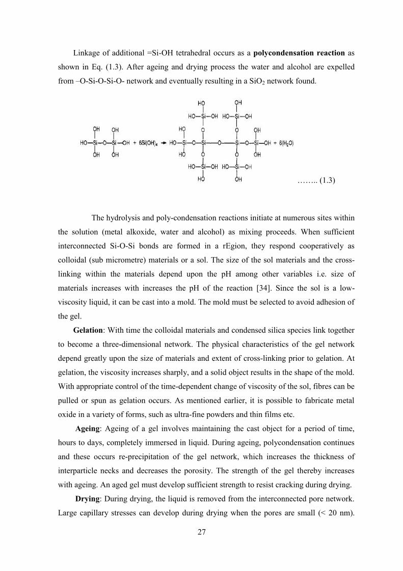
1.4.9. Sol-Gel Process
Sol and Gel have are used scientific interests for a long time and may be defined
as follows: State of distribution of colloid (solid materials with size 1-1000 nm,
include103-109 atoms) materials in liquid state is called sol and the colloid materials,
through van der Waals attraction, eventually connect to form a gel, a 3-dimensional solid
network having high porosity and high specific surface area and this process is known
from long times. The first silica gels were made in 1845 by M. Ebelmen in France and the
oldest sols prepared in a laboratory were synthesized with gold [30]. In the 1950s and
26
1960s, Roy and co-workers [31] used sol-gel method to synthesize a variety of novel metal
oxide compositions with very high levels of chemical homogeneity, including Si, Al, Zr,
Nd etc, which could not be made using traditional oxide powder methods [32]. The sol-gel
method is a wet-chemical synthesis technique for preparation of glasses, ceramics and
nanoparticles at low temperature. It is based on control of hydrolysis and condensation of
alkoxide precursors. It is possible to fabricate metal oxide in a variety of forms, such as