57
1 Chapter 1 Introduction * Many slides are from the authors
| Date post: | 01-Jan-2016 |
| Category: |
Documents |
| Upload: | kirby-church |
| View: | 14 times |
| Download: | 0 times |

1
Chapter 1Introduction
* Many slides are from the authors

1.0 BACKGROUND
2

3
Why study logic design? it is the implementation basis for all modern computing devices
building large things from small components provide a model of how a computer works
More important reasons the inherent parallelism in hardware is often our first exposure to
parallel computation it offers an interesting counterpoint to software design and is
therefore useful in furthering our understanding of computation, in general

4
Applications of logic design Conventional computer design
CPUs, busses, peripherals Networking and communications
phones, modems, routers Embedded products
in cars, toys, appliances, entertainment devices Scientific equipment
testing, sensing, reporting The world of computing is much bigger than just PCs!

5
Global processor/controller market
PC CPUs constitute less than 2% of the market

1.1 DISSECTING THE TITLE
6
7
What is design? (1/2) Design is the process of coming up with a solution to a
problem Engineering, art,…
What is needed for design? Understand the problem
Requirements: functional vs. non-functional (performance) Understand the constraints
E.g., criteria for size, cost, power, beauty, etc.
For a complex problem, a divide-and-conquer approach E.g. dividing a building into constituent components
Office layouts, window frames, ventilation systems etc. E.g. India and Pakistan

8
What is design? (2/2) Software design
Hardware platform imposes a limitation Break down software into pieces Reuse utilities Put together all the pieces
Designing a complex system requires a design methodology Design methodology
Domain-specific formalization of the design process into a set of well understood steps
Three facets: creativity, tradeoff (decisions among alternatives), optimization
Q: Tradeoffs in highway construction?

9
What is logic design? (1/2) Digital hardware consists of components as well Components or building blocks
Switches built from semiconductor transistors Most basic element
Higher level circuits such as logic gates and memories Switches and wires
A logic designer should choose the right component to solve logic design problems
Constraints: size, cost, performance, power consumption Cost vs. size
* A circuit is an interconnected collection of switches

10
What is logic design? (2/2) Each component has
a set of input wires a set of output wires Each wire is set to some analog voltage value
But will be interpreted as either 1 or 0 (digital abstraction)
Transistors react to the voltage levels on the input wires Switch their state and cause a change in output wires At macro scale, a component that contains transistors reacts to
input voltage values Depending on the way a circuit reacts to the input voltages
Combinational logic circuits Sequential logic circuits
11
sense
sense
driveAND
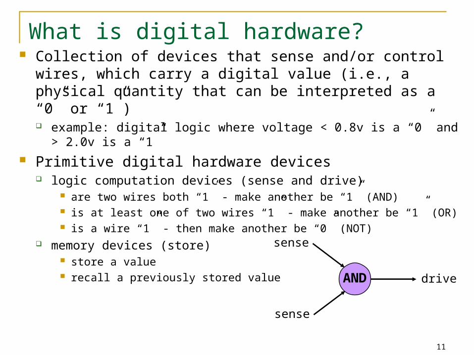
What is digital hardware? Collection of devices that sense and/or control wires, which
carry a digital value (i.e., a physical quantity that can be interpreted as a “0” or “1”) example: digital logic where voltage < 0.8v is a “0” and > 2.0v is a “1”
Primitive digital hardware devices logic computation devices (sense and drive)
are two wires both “1” - make another be “1” (AND) is at least one of two wires “1” - make another be “1” (OR) is a wire “1” - then make another be “0” (NOT)
memory devices (store) store a value recall a previously stored value

1.3 COMPUTATION
12

13
Computation: abstract vs. implementation Computation has been a mental exercise (paper, programs)
This class is about physically implementing computation using physical devices that use voltages to represent logical values
Basic units of computation are: representation: "0", "1" on a wire
set of wires (e.g., binary integer)
assignment: x = y data operations: x + y – 5 control:
sequential statements: A; B; Cconditionals: if (x == 1) then y;loops: for ( i = 1 ; i == 10; i++)procedures: A; proc(...); B;
We will study how each of these are implemented in hardware and composed into computational structures
14
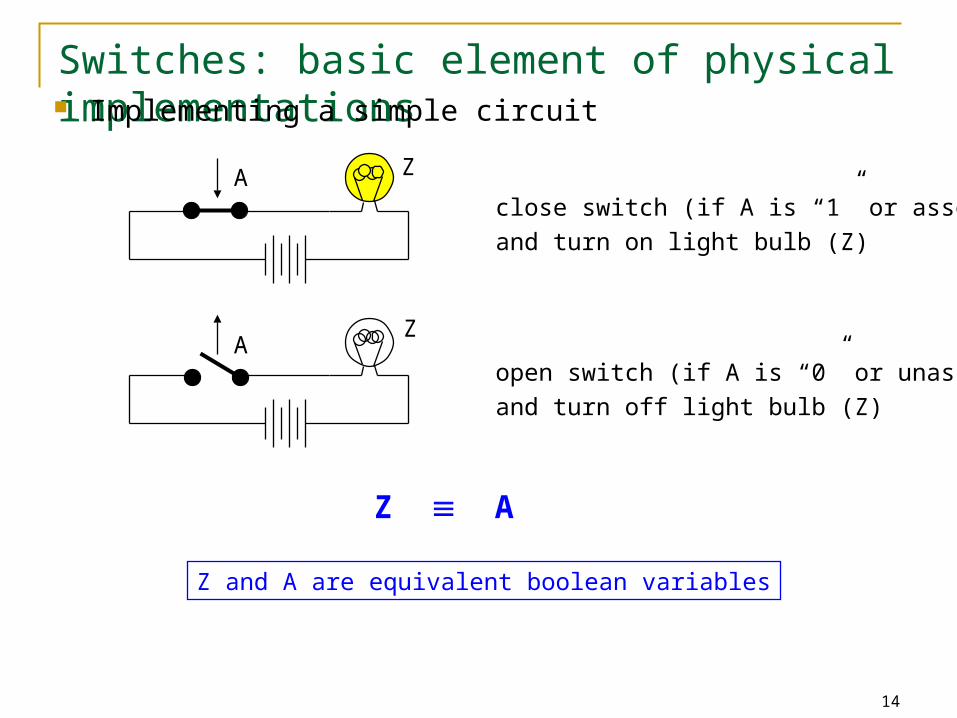
close switch (if A is “1” or asserted)and turn on light bulb (Z)
A Z
open switch (if A is “0” or unasserted)and turn off light bulb (Z)
Switches: basic element of physical implementations Implementing a simple circuit
Z A
AZ
Z and A are equivalent boolean variables

15
AND
OR
Z A and B
Z A or B
A B
A
B
Switches (cont’d) Compose switches into more complex ones (Boolean
functions):
16
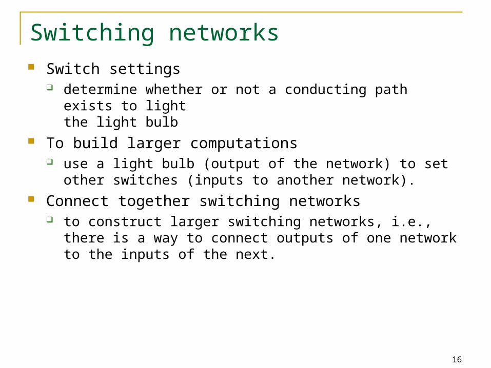
Switching networks Switch settings
determine whether or not a conducting path exists to light the light bulb
To build larger computations use a light bulb (output of the network) to set other switches
(inputs to another network). Connect together switching networks
to construct larger switching networks, i.e., there is a way to connect outputs of one network to the inputs of the next.

17
A switch? A mechanical switch
A semiconductor switch or transistor
In the earliest days of digital circuits, a relay is used to implement a switch

18
conductingpath composed
of switchescloses circuit
2. current flowing through coil magnetizes core and causes normally closed (NC) contact to be pulled open
1. when no current flows, the spring of the contact returns it to its normal position
Relay networks A simple way to convert between conducting paths and
switch settings is to use (electro-mechanical) relays. What is a relay?
Relay = magnet + switch Both electric and mechanical properties The lower flexible half of the switch is made of ferric material Slow and large
1
* Ferric: 철분<- Ferrum (Fe)
2
electromagnet
19
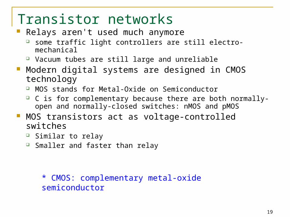
Transistor networks Relays aren't used much anymore
some traffic light controllers are still electro-mechanical Vacuum tubes are still large and unreliable
Modern digital systems are designed in CMOS technology MOS stands for Metal-Oxide on Semiconductor C is for complementary because there are both normally-open
and normally-closed switches: nMOS and pMOS MOS transistors act as voltage-controlled switches
Similar to relay Smaller and faster than relay
* CMOS: complementary metal-oxide semiconductor
20
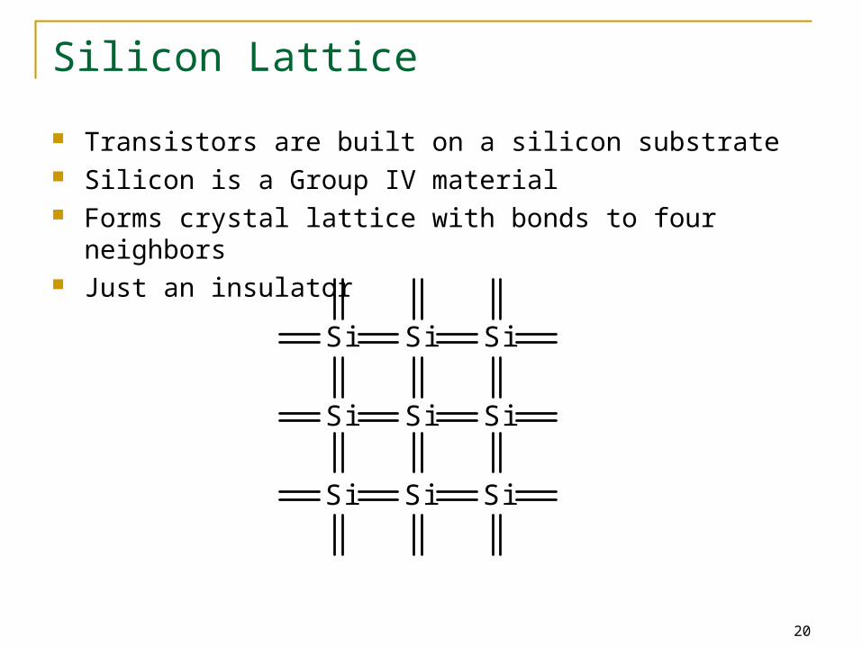
Silicon Lattice
Transistors are built on a silicon substrate Silicon is a Group IV material Forms crystal lattice with bonds to four neighbors Just an insulator
Si SiSi
Si SiSi
Si SiSi
21
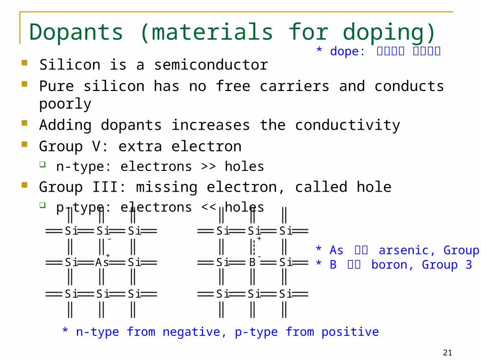
Dopants (materials for doping) Silicon is a semiconductor Pure silicon has no free carriers and conducts poorly Adding dopants increases the conductivity Group V: extra electron
n-type: electrons >> holes Group III: missing electron, called hole
p-type: electrons << holes
As SiSi
Si SiSi
Si SiSi
B SiSi
Si SiSi
Si SiSi
-
+
+
-* As 비소 arsenic, Group 5* B 붕소 boron, Group 3
* n-type from negative, p-type from positive
* dope: 불순물을 첨가하다

22
p-n Junctions
A junction between p-type and n-type semiconductor forms a diode.
Current flows only in one direction
p-type n-type
anode cathode
current
+ V - V
Anode: 양극 ana (up) + hodos (way)Cathode: 음극 kata (down) + hodos (way)

23
n-channel (or n-type) MOS (nMOS) circuit Three terminals: source-gate-drain (or S-G-D for short) three layers: polysilicon (used to be metal) – SiO2 - substrate
n+
p
GateSource Drain
bulk Si
SiO2
Polysilicon
n+
* n+: heavily doped n-type semiconductor
If G is at positive voltage, electrons in the substrate will move toward G terminal, which sets up a channel between S and D And D is at high voltage, current will flow from drain to source
Metal is replaced by polysilicon which is more adhesive
* oxide 산화물

24
p-channel (or p-type) MOS (pMOS) circuit Three terminals: source-gate-drain (or S-G-D for short) Same principle, but reverse doping and voltage
Source (Vss) is positive with regard to drain (Vdd) Bubble indicates the inverted behavior
If G is at positive voltage, the current does not flow If G is at ground level, the current flows
SiO2
n
GateSource Drain
bulk Si
Polysilicon
p+ p+

25
n-channelopen when voltage at G is low
closed when voltage at G is high
p-channelclosed when voltage at G is lowopen when voltage at G is high
MOS transistors MOS transistors have three terminals: drain, gate, and source
they act as switches in the following way:if the voltage on the gate terminal is (some amount) higher/lower than the source terminal, then a conducting path will be established between the drain and source terminals
G
S D
G
S D

26
3v
X
Y 0 volts
x y
3 volts0v
what is the relationship
between x and y?
MOS networks
0 volts
3 volts
A simple component is made up of two transistors X: input Y: output What is this function?
In CMOS circuits, pMos and nMOS are used in pair

27
x y z1 z2
0 volts
3 volts
0 volts
3 volts
0 volts
0 volts
3 volts
3 volts
what is the relationship between x, y and z1/z2?
Two input networks
3v
X Y
0v
Z1
0v
3v
X Y
Z2
3 volts
3 volts
3 volts
0 volts
3 volts
0 volts
0 volts
0 volts
NAND NOR

28
Three input NAND gate
A
B
Y
C
Y pulls low if ALL inputs are 1 Y pulls high if ANY input is 0
VDD
In general, the more inputs, the more transistors (TRs) In CMOS, a variable requires a pair of TRs

29
Digital vs. analog Convenient to think of digital systems as having only
discrete (or digital) input/output values In reality, real electronic components exhibit
continuous, analog behavior Why do we make the digital abstraction anyway?
switches operate this way easier to think about a small number of discrete values Quantization error, though
Why does it work? does not propagate small errors in values always resets to 0 or 1
P.14

30
Technology State 0 State 1
Relay logic Circuit Open Circuit ClosedCMOS logic 0.0-1.0 volts 2.0-3.0 voltsTransistor transistor logic (TTL) 0.0-0.8 volts 2.0-5.0 voltsFiber Optics Light off Light onDynamic RAM Discharged capacitor Charged capacitorNonvolatile memory (erasable) Trapped electrons No trapped electronsProgrammable ROM Fuse blown Fuse intactMagnetic disk No flux reversal Flux reversalCompact disc No pit Pit
Mapping from physical world to binary world

31
inputs outputssystem
Combinational vs. sequential digital circuits A simple model of a digital system is a unit with inputs and
outputs:
Combinational means "memory-less" a digital circuit is combinational if its output values
only depend on its (current) input values
32
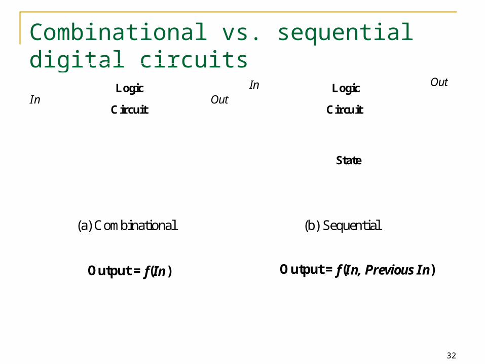
Combinational vs. sequential digital circuits
Logic
Circuit
Logic
CircuitOut
OutInIn
(a) Combinational (b) Sequential
State
Output = f(In) Output = f(In, Previous In)

33
easy to implementwith CMOS transistors(the switches we haveavailable and use most)
Combinational logic symbols Common combinational logic systems have standard symbols called logic gates
Buffer, NOT
AND, NAND
OR, NORZ
AB
Z
Z
A
AB
34
Sequential logic Sequential systems
exhibit behaviors (output values) that depend not only on the current input values, but also on previous input values
In reality, all real circuits are sequential because the outputs do not change instantaneously after an
input change Timing is important
A fundamental abstraction of digital design is to reason (mostly) about steady-state behaviors look at the outputs only after sufficient time has elapsed for the
system to make its required changes and settle down

35
B
AC
Clock
Example of combinational and sequential logic Combinational:
input A, B wait for clock edge observe C wait for another clock edge observe C again: will stay the same
Sequential: input A, B wait for clock edge observe C wait for another clock edge observe C again: may be different
36
Abstractions Some we've seen already
digital interpretation of analog values transistors as switches switches as logic gates use of a clock to realize a synchronous sequential circuit
Some others we will see truth tables and Boolean algebra to represent combinational logic encoding of signals with more than two logical values into
binary form state diagrams to represent sequential logic hardware description languages to represent digital logic waveforms to represent temporal behavior

1.4 examples
37

38
An example Calendar subsystem: number of days in a month (to control watch display)
Combinational logic
used in controlling the display of a wrist-watch LCD screen
inputs: month, leap year flag
outputs: number of days

39
Implementation in softwareinteger number_of_days ( month, leap_year_flag)
{switch (month) {
case 1: return (31);
case 2: if (leap_year_flag == 1) then return (29) else return (28);
case 3: return (31);
...
case 12: return (31);
default: return (0);
}
}
P.16

40
leapmonth
d28d29d30d31
month leap d28 d29 d30 d310000 – – – – – 0001 – 0 0 0 10010 0 1 0 0 00010 1 0 1 0 00011 – 0 0 0 10100 – 0 0 1 00101 – 0 0 0 10110 – 0 0 1 00111 – 0 0 0 11000 – 0 0 0 11001 – 0 0 1 01010 – 0 0 0 11011 – 0 0 1 01100 – 0 0 0 11101 – – – – –111– – – – – –
Implementation as a combinational digital system Encoding:
how many bits for each input/output? binary number for month four wires for 28, 29, 30, and 31
Behavior: combinational truth table
specification
Don’t care

41
Truth-table to logic to switches to gates d28 = 1 when month=0010 and leap=0 d28 = m8'•m4'•m2•m1'•leap'
d31 = 1 when month=0001 or month=0011 or ... month=1100 d31 = (m8'•m4'•m2'•m1) + (m8'•m4'•m2•m1) + ...
(m8•m4•m2'•m1') d31 = can we simplify more?
symbol for and
symbol for or
symbol for not
Combinational example (cont’d)
month leap d28 d29 d30 d310001 – 0 0 0 10010 0 1 0 0 00010 1 0 1 0 00011 – 0 0 0 10100 – 0 0 1 0...1100 – 0 0 0 11101 – – – – –111– – – – – –0000 – – – – –

42
Combinational example (cont’d) d28 = m8'•m4'•m2•m1'•leap’ d29 = m8'•m4'•m2•m1'•leap d30 = (m8'•m4•m2'•m1') + (m8'•m4•m2•m1') +
(m8•m4'•m2'•m1) + (m8•m4'•m2•m1) = (m8'•m4•m1') + (m8•m4'•m1)
d31 = (m8'•m4'•m2'•m1) + (m8'•m4'•m2•m1) + (m8'•m4•m2'•m1) + (m8'•m4•m2•m1) + (m8•m4'•m2'•m1') + (m8•m4'•m2•m1') + (m8•m4•m2'•m1')

43
Combinational example (cont’d) d28 = m8'•m4'•m2•m1'•leap’ d29 = m8'•m4'•m2•m1'•leap d30 = (m8'•m4•m2'•m1') + (m8'•m4•m2•m1') +
(m8•m4'•m2'•m1) + (m8•m4'•m2•m1) d31 = (m8'•m4'•m2'•m1) + (m8'•m4'•m2•m1) +
(m8'•m4•m2'•m1) + (m8'•m4•m2•m1) + (m8•m4'•m2'•m1') + (m8•m4'•m2•m1') + (m8•m4•m2'•m1')

44
Another example (Door combination lock) punch in 3 values in sequence and the door opens; if there is
an error the lock must be reset; once the door opens the lock
must be reset
Sequential logic
inputs: sequence of input values, reset
Numeric number: 4 wires
outputs: door open/close
memory: must remember combination
or always have it available as an input

45
Implementation in softwareinteger combination_lock ( ) {
integer v1, v2, v3;integer error = 0;static integer c[3] = 3, 4, 2;
while (!new_value( ));v1 = read_value( );if (v1 != c[1]) then error = 1;
while (!new_value( ));v2 = read_value( );if (v2 != c[2]) then error = 1;
while (!new_value( ));v3 = read_value( );if (v2 != c[3]) then error = 1;
if (error == 1) then return(0); else return (1);
}
P.19, 20
Array index starts from 1

46
Implementation as a sequential digital system Encoding:
how many bits per input value? how many values in sequence? how do we know a new input value is entered? how do we represent the states of the system?
Behavior: clock wire tells us when it’s ok
to look at inputs(i.e., they have settled after change)
sequential: sequence of valuesmust be entered
sequential: remember if an error occurred finite-state specification
resetvalue
open/closed
new
clockstate

47
C2!=value& new
C3!=value& new
reset
not newnot newnot new
closed
S1
closedC1=value
& new
S2
closedC2=value
& new
S3
C3=value& new
OPEN
open
C1!=value& new
closed
ERR
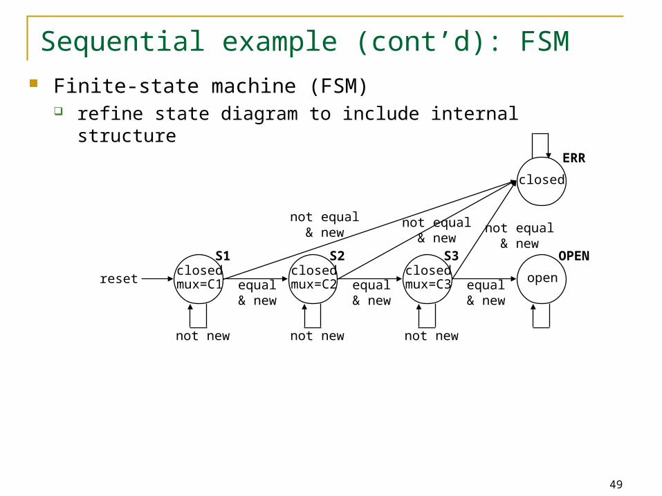
Sequential example (cont’d): abstract control
Finite-state diagram states: 5 states
represent point in execution of machine each state has inputs and outputs
transitions: 6 from state to state, 5 self transitions, 1 global changes of state occur when clock says it’s ok based on value of inputs
inputs: reset, new, results of comparisons output: open/closed
48
reset
open/closed
new
C1 C2 C3
comparator
value
equal
multiplexer
equal
controllermux control
clock
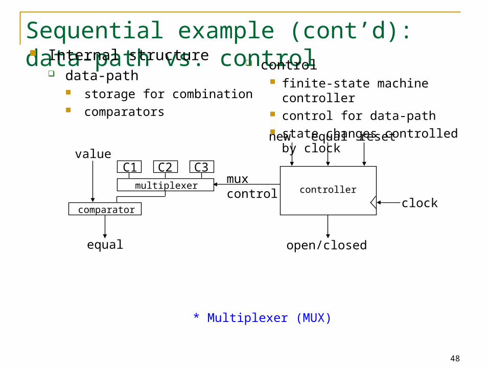
Sequential example (cont’d): data-path vs. control Internal structure
data-path storage for combination comparators
control finite-state machine controller control for data-path state changes controlled by clock
* Multiplexer (MUX)
49
closed
closedmux=C1reset equal
& new
not equal& new
not equal& new
not equal& new
not newnot newnot new
S1 S2 S3 OPEN
ERR
closedmux=C2 equal
& new
closedmux=C3 equal
& new
open
Sequential example (cont’d): FSM Finite-state machine (FSM)
refine state diagram to include internal structure

50
reset new equal state state mux open/closed1 – – – S1 C1 closed0 0 – S1 S1 C1 closed0 1 0 S1 ERR – closed0 1 1 S1 S2 C2 closed0 0 – S2 S2 C2 closed0 1 0 S2 ERR – closed0 1 1 S2 S3 C3 closed0 0 – S3 S3 C3 closed0 1 0 S3 ERR – closed0 1 1 S3 OPEN – open 0 – – OPEN OPEN – open0 – – ERR ERR – closed
next
Sequential example (cont’d): FSM Finite-state machine
generate state table (much like a truth-table)closed
closedmux=C1
reset equal& new
not equal& new
not equal& new
not equal& new
not newnot newnot new
S1 S2 S3 OPEN
ERR
closedmux=C2 equal
& new
closedmux=C3 equal
& new
open
* state is not input, but internal variable
51
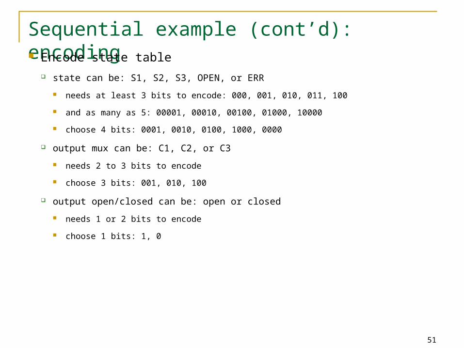
Sequential example (cont’d): encoding Encode state table
state can be: S1, S2, S3, OPEN, or ERR
needs at least 3 bits to encode: 000, 001, 010, 011, 100
and as many as 5: 00001, 00010, 00100, 01000, 10000
choose 4 bits: 0001, 0010, 0100, 1000, 0000
output mux can be: C1, C2, or C3
needs 2 to 3 bits to encode
choose 3 bits: 001, 010, 100
output open/closed can be: open or closed
needs 1 or 2 bits to encode
choose 1 bits: 1, 0

Internal input
Encode state table state can be: S1, S2, S3, OPEN, or ERR
choose 4 bits: 0001, 0010, 0100, 1000, 0000 output mux can be: C1, C2, or C3
choose 3 bits: 001, 010, 100 output open/closed can be: open or closed
choose 1 bits: 1, 0
52
good choice of encoding!
mux is identical to last 3 bits of next state
open/closed isidentical to first bitof state
Sequential example (cont’d): encoding
reset new equal state state mux open/closed1 – – – 0001 001 0 0 0 – 0001 0001 001 00 1 0 0001 0000 – 00 1 1 0001 0010 010 0 0 0 – 0010 0010 010 00 1 0 0010 0000 – 00 1 1 0010 0100 100 0 0 0 – 0100 0100 100 00 1 0 0100 0000 – 00 1 1 0100 1000 – 1 0 – – 1000 1000 – 10 – – 0000 0000 – 0
next
Internal output
system’s or external
output
external input

53
reset
open/closed
new equal
controllermux control
clockreset
open/closed
new equal
mux control
clock
comb. logic
state
special circuit element, called a register, for
remembering inputs when told to by clock
Sequential example (cont’d): controller implementation Implementation of the controller

54
system
data-path control
stateregisters
combinationallogic
multiplexer comparatorcoderegisters
register logic
switchingnetworks
Design hierarchy

Further Remarks
55

56
terminologies
n+n+S
GD
+
DEVICE
CIRCUIT
GATE
MODULE
SYSTEM

57
Summary
That was what the entire course is about
converting solutions (to problems) into combinational and
sequential networks effectively organizing the design
hierarchically
doing so with a modern set of design tools that lets us handle
large designs effectively
taking advantage of optimization opportunities


