Page 1
1
Chapter 1 : Introduction
1.1 Benefits of MOSFET Scaling
Computing power has increased dramatically over the decades, enabled by
significant advances in silicon integrated circuit (IC) technology led by the continued
miniaturization of the MOS transistor. The rapid progress in the semiconductor industry
has been driven by improved circuit performance and functionality together with reduced
manufacturing costs. Since the 1960s, MOS transistor dimensions have been shrinking
30% every 3 years, as predicted by Moore’s law [1] depicted in Figure 1.1 [2] and scaling
has in fact accelerated recently [3].
While Moore’s Law only describes the rate of increase in transistor density,
reduction of the physical MOS device dimensions has improved both circuit speed and
density in the following ways: a) Circuit operational frequency increases with a reduction
in gate length, LG, as ~ 1/LG; allowing for faster circuits, b) Chip area decreases ~ LG2;
enabling higher transistor density and cheaper ICs. c) Switching power density ~
constant; allows lower power per function or more circuits at the same power.
Device scaling has been a relatively straightforward affair thus far, but physical
limits are fast being approached, and new materials and device structures are needed to
continue scaling trends.
Page 2
2
Figure 1.1: Moore’s law of scaling. The number of transistors on a chip has been
increasing exponentially [1, 2]
1.2 Issues in Planar Bulk-Si MOSFET Scaling
The planar bulk-silicon MOSFET has been the workhorse of the semiconductor
industry over the last 40 years. However, the scaling of bulk MOSFETs becomes
increasingly difficult for gate lengths below ~20nm (sub-45 nm half-pitch technology
node) expected by the year 2009. As the gate length is reduced, the capacitive coupling of
the channel potential to the source and drain increases relative to the gate, leading to
significantly degraded short-channel effects (SCE). This manifests itself as a) increased
off-state leakage, b) threshold voltage (VTH) roll-off, i.e. smaller VTH at shorter gate
lengths, and c) reduction of VTH with increasing drain bias due to a modulation of the
source-channel potential barrier by the drain voltage, also called drain-induced barrier
lowering (DIBL). In order to maintain the relatively strong gate control of the channel
Page 3
3
potential in bulk devices, various technological improvements such as ultra-thin gate
dielectrics, ultra-shallow source/drain junctions, halo implants and advance channel
dopant profile engineering techniques such as super-steep retrograde wells have been
necessary. Each of these technologies is now approaching fundamental physical
limitations which may, in turn, limit further scaling of device dimensions.
In MOS devices, the gate dielectric thickness is single most important device
dimension to enable device scaling and has also been the most aggressively scaled one. A
thin gate dielectric increases capacitive coupling from the gate to the channel, thereby
reducing the source/drain influence on the channel. A larger gate capacitance also leads
to a larger inversion charge density, or increased ON-state drive current. However, gate
dielectrics are already so thin that quantum mechanical direct tunneling through them
results in significant gate leakage currents below ~20Å. The use of alternative high-
κ gate dielectric materials can provide a small effective oxide thickness to maintain
adequate gate control needed for LG scaling while providing a large physical barrier to
gate-oxide tunneling, thereby reducing gate leakage.
Reduction of the source/drain extension junction depth directly decreases
capacitive coupling of the drain to the channel, thus also reduces drain-induced short-
channel effects. Shallow source/drain junction formation requires that low-energy ion
implantation together with low thermal budget dopant activation to minimize dopant
diffusion. The downside to this is the increase in the parasitic series resistance of the
source and drain extension regions. Raised source/drain technologies can alleviate the
extrinsic resistance problem while maintaining shallow junctions. The contact resistance
associated with the metallic contacts to the source/drain regions is another source for
Page 4
4
parasitic series resistance and is expected to dominate the total parasitic resistance of the
device.
In order to scale bulk-Si transistors, heavy body doping is also necessary to
eliminate leakage paths far from the gate dielectric interface and to increase back-gate
(substrate) control of the body. For sub-100nm gate length devices, a strong halo implant
is generally used to suppress sub-surface leakage, but this tends to increase the average
channel doping in small LG devices. However, high channel doping concentration,
however, reduces carrier mobility due to impurity scattering and increased transverse
electric field, increases subthreshold slope, enhances band-to-band tunneling leakage, and
increases depletion and junction capacitances. These factors may combine to significantly
degrade device performance.
In summary, from a device design point of view, in order to achieve good
electrostatic integrity or good control of short-channel effects (SCE), the gate dielectric
thickness, TOX, the source/drain junction depth, XJ, and the channel depletion depth XDEP,
need to be scaled down. The scale length for a bulk device, λBULK, is an indication of how
short LG can be made before the SCE are excessive, and is quantitatively expressed in Eq.
1-1. For good electrostatic control, the minimum LG should be no less than ~ 5λBULK. [4]
( ) 312
DEPJOXBULK XXT1.0=λ Eq. 1-1
For a bulk MOSFET, gate leakage limits TOX scaling, XDEP scaling is limited to
about 10 nm due to substrate-to-drain band-to-band tunneling current limitations on body
doping, and XJ is limited by process limits for forming ultra shallow junctions with abrupt
doping profiles. Experimental bulk MOSFETs have been demonstrated down to 5nm LG
[5]. However, the performance did not meet industry roadmap specifications [6],
Page 5
5
especially for low power applications. Continued device scaling will require new
materials and/or alternative MOSFET structures. Therefore bulk MOSFET scaling is
becoming increasingly harder and new transistor designs offering better scalability are
needed. These are introduced in the next section.
The IC industry has started to deploy circuit design and architectural techniques
such as multiple cores and multiple threads that exploit parallelism to improve the overall
chip performance, enhance the chip functionality while maintaining chip power density
and total chip power dissipation at a manageable level. With more than one central
processing unit (CPU) core on chip, the cores can each be clocked at a lower frequency
while still providing for better overall chip performance. In addition, ever more cache
memory is being added onto the processor chip in order to minimize the system
performance penalty associated with finite-cache effects. With the shift to multi-core
processing becoming increasingly important, the performance of each core can be
correspondingly lower, meaning that lower leakage (vs. high performance) MOSFET
designs will become increasingly important because the desired overall chip performance
can be achieved through parallelism.
1.3 Process-induced Variations
Control of critical dimensions (CDs) such as LG continues to be a difficult
challenge, as the physical gate length is considerably smaller than the lithography printed
linewidth. Controlling the lithography and etch processes to achieve critical dimension
control to within 10% (3s ), as prescribed in the 2003 International Roadmap for
Semiconductors (ITRS) [7] is almost universally unachievable, so the CD tolerance has
Page 6
6
been increased to 12% (3s ) in 2005[6]; there might be a need to relax this requirement
further in the future.
In order to limit the impact of variations, the semiconductor is industry is actually
using slightly larger physical gate lengths than those specified in the ITRS, especially for
memory applications [8]. The slowing down of LG scaling may be unavoidable in the
future since the control of process variables does not track the scaling of minimum
feature sizes. This is of particular importance for memory arrays, because if the desired
degree of dimensional control were not achievable, design margins would need to be
relaxed to achieve large functional memory arrays. This slowdown in technology scaling
will probably be application specific, and is unavoidable if process-control is not robust
enough.
Figure 1.2: Changes in physical gate length, lithography tolerance, and etch tolerance
over the years. The physical gate length tolerance has been relaxed to 12%, and this trend
is expected to continue. [9]
Page 7
7
While advanced process control can minimize systematic shifts in the CD, the
role of random variations arising from statistical dopant fluctuations and line edge
roughness is expected to increase, so that variations will impact the overall power
dissipation and performance [10]. Therefore, statistical treatment of random variation of
circuits (statistical design) is becoming increasingly important. New transistor structures
should have better immunity to process variations, and devices with tunable VTH are
beneficial to counter any systematic shifts in transistor characteristics.
1.4 Thin-body MOSFETs
Si Substrate
G
Source Drain
LG
BOX
G
Source Drain
LG
TSi
G
Source Drain
G
LG
TSi
(a) Bulk-Si MOSFET (b) UTB MOSFET (c) DG MOSFET
Figure 1.3: Advanced transistor structures such as the UTB and the DG-MOSFET
eliminate sub-surface leakage paths and extend the scalability of Si CMOS technology.
As the bulk MOSFET is scaled down, the control of short channel effects
becomes increasingly difficult leading to increased subthreshold leakage current. This is
because the source/drain influence over the channel potential becomes significant relative
to the gate control.
From Eq. 1-1, it is clear that if XJ and XDEP can be reduced aggressively, it is
possible to scale the MOSFET down to very small LG. This is precisely what is done in
Page 8
8
the case of ultra-thin body (UTB) silicon-on-insulator (SOI) devices, where XJ and XDEP
are physically limited to the thickness of an ultra-thin silicon film. Eq. 1-1 only
qualitatively describes the scaling behavior of UTB, and better models are introduced
later. Thus, the scalability of MOS devices can be improved by using an ultra thin silicon
body such that all points in the silicon channel are close enough to the gate and well
controlled by it, thereby eliminating sub-surface leakage currents. The conventional fully
depleted SOI MOSFET (with a thick body) is known to have worse short-channel effects
than bulk MOSFETs and partially depleted SOI MOSFETs [11]. To achieve good short
channel control, TSi must be smaller than the depletion width or junction depth of a
comparable bulk device with high channel doping. The leakage path in a UTB device is
along the buried-oxide interface, furthest away from the gate. The thinner the silicon
body is made, the larger is the leakage reduction from eliminating sub-surface leakage
paths far away from the gate, and the better the device scalability. Also, UTB devices do
not have the floating body effects seen in thick (partially-depleted) SOI devices (PDSOI),
because there is no floating quasi-neutral region in the body.
The body thinness requirement can be relaxed by adopting the double-gate (DG)
MOSFET structure shown in Figure 1.3c, in which two gates control the channel
potential. The DG-FET achieves better gate control and thereby has improved SCE for a
given body thickness [12]. The body thickness can be twice that of a single-gated UTB
device, in order to achieve the same degree of SCE. The DG MOSFET does not suffer
from electric field penetration from the source/drain to the channel through the buried
oxide and is therefore more scalable. The relaxed thinness requirement for the body is
highly desirable from a manufacturability point of view, since the formation of a uniform
Page 9
9
ultra-thin film can pose major technological challenges. Simulation results show that a
DG MOSFET has the best scalability, down to sub-10nm LG devices [13]. The improved
scalability of thin-body devices makes them attractive for future generations of CMOS
technology and so they have been included in the International technology roadmap for
semiconductors (ITRS) (see Figure 1.4) [6].
Figure 1.4: Advanced transistor designs may be necessary to meet performance
requirements. Potential timetable for the adoption of advanced device structures to meet
performance requirements. [6, 9]
UTB devices can be implemented in a straightforward manner as planar single
gate fully depleted silicon-on-insulator (FDSOI) devices [14-19]. While the planar
double-gate device has been demonstrated [20], the fabrication of a planar double-gate
FET with a bottom gate that is aligned to the top gate and source/drain regions imposes
numerous process challenges. Among all DG structures proposed so far, the FinFET
(Figure 1.5) is the most manufacturable because it eliminates the need for the bottom gate
by rotating the channel by 90 and placing the gate electrodes on the two sidewalls of the
silicon fin [21-23]. Independent gate FinFETs, in which the front and back-gate
electrodes can be independently biased have been demonstrated as well [24, 25]. The
front gate can be used to switch the device, whereas the back-gate can be used to set the
Page 10
10
correct VTH. The back-gate is as strong as the front gate, and therefore the device has
degraded sub-threshold slope and transconductance due to a capacitive division of the
channel potential between the two gates, however.
Source
Drain Gate
LG TSi
HFin
Figure 1.5: The FinFET consists of a thin Si fin, with the gate running over the fin in a
self-aligned fashion. The gate controls the channel along the sidewalls of the fin and the
width of the channel is defined by twice the height of the fin, HFIN.
The planar FDSOI MOSFET can been extended to include a conducting electrode
underneath the buried oxide (BOX) layer to form a second gate to control the channel
from below [26]. This ground plane or the back-gate acts as a second gate to shield the
field penetration from the drain into the channel, and improves SCE. In a way, it serves
the role of the retrograde doping in a bulk MOSFET, by raising the body backside
potential and by terminating drain electric fields [12]. In addition, the BOX eliminates
source/drain-to-substrate depletion capacitance. In order to prevent electric field
penetration through the BOX, the BOX layer should be thin. Another benefit of a thin
Page 11
11
BOX is the “back-gate effect,” similar to the “body effect” in bulk-Si devices, wherein
the VTH can be tuned by the back-gate voltage (Figure 1.6). However, the subthreshold
slope and the transconductance are degraded due to the capacitive division of the channel
potential between the front- and the back-gate potentials.
Figure 1.6: Back-gate effect in BG-FDSOI device showing VTH tunability. The upper and
lower limits of the tunable VTH range are set by the back interface entering either
inversion or accumulation.
While the early FinFET devices were fabricated on SOI wafers, FinFETs on bulk-
Si wafers have been demonstrated as well [27, 28]. Bulk-FinFETs have the advantages of
being potentially cheaper and can be easily integrated with conventional bulk-Si CMOS
technology. Bulk FinFETs combine the benefits of good leakage and short-channel
control together with a cheaper manufacturing process, making them attractive for high-
density memory applications.
Page 12
12
2
4
68
10
20 Bulk UTB DG
Technology Lgate [nm]
FO
4 In
vert
er D
elay
[p
s]
50 35 25 18
TSi,UTB = 5nm
TSi,UTB < 5nm
Figure 1.7: DG and UTB devices show better delay than planar bulk devices. The
improved performance is due to a combination of improved subthreshold swing, higher
carrier mobility, and reduced inversion capacitance and parasitic capacitances.
The main benefits of thin body devices are improved transistor subthreshold
swing due to greatly improved gate control, improved channel mobility due to reduced
transverse electric field, reduced parasitic capacitances from the absence of depletion
capacitances, leading to improved speed, and reduced power consumption. While the
FinFET shows the largest performance benefits, the UTB device shows slightly degraded
subthreshold swing and degraded ON-currents resulting in larger gate delays (Figure 1.7).
[29]. The BG-FDSOI device, with its large back-gate effect and nonideal subthreshold
swing, is expected to be slower than FinFET. However, it has the benefit of adaptive VTH
control, which is a promising way to limit the effect of variations.
Strained Si technology has been very successful in boosting the performance of
both NMOS and PMOS devices, through enhancement in carrier mobilities. Popular
Page 13
13
approaches consist of local channel stressing from uniaxial stress induced by Si1-xGex
source/drain regions for PMOS devices and from global stress induced by capping layers
formed after gate patterning. While NMOS devices primarily benefit from tensile stress,
compressive stress is beneficial in PMOS devices. The effect of biaxial and uniaxial
stresses on transistor performance is now starting to be well understood [30]. UTB and
FinFET devices can each benefit from a combination of local and global stresses. While
it is harder to implement uniaxial stress from source/drain regions using Si1-xGex regions,
stressed capping layers and gate electrode induced stress can be beneficial for boosting
performance in FinFET devices [31, 32].
The main challenge with bringing UTB and FinFETs into manufacturing is the
ability to form thin silicon channels with very good thickness uniformity. Fluctuations in
the body thickness can cause spread in the VTH and other device characteristics. Series
resistance is a big source of performance degradation in FDSOI devices and FinFETs,
and so technologies such as raised source/drain achieved through selective epitaxy or
deposition are needed to make low resistance contacts [12]. These technologies have
been investigated and process solutions have been identified. [17, 23]
1.5 SRAM Scaling Issues
Static random access memory (SRAM) is by far the dominant form of embedded
memory found in today’s integrated circuits (ICs) occupying as much as 60-70% of the
total chip area and about 75%-85% of the transistor count in some IC products. The most
commonly used memory cell design uses six transistors (6-T) to store a bit, so all of the
issues associated with MOSFET scaling apply to scaling of SRAM. As memory will
continue to consume a large fraction of the area in many future IC chips, scaling of
Page 14
14
memory density must continue to track the scaling trends of logic. [33]. Statistical dopant
fluctuations, variations in oxide thickness, and line-edge roughness increase the spread in
transistor threshold voltage and thus the on- and off- currents as the MOSFET is scaled
down in the nanoscale regime [34]. Increased transistor leakage and parameter variations
present the biggest challenges for the scaling of 6-T SRAM memory arrays.
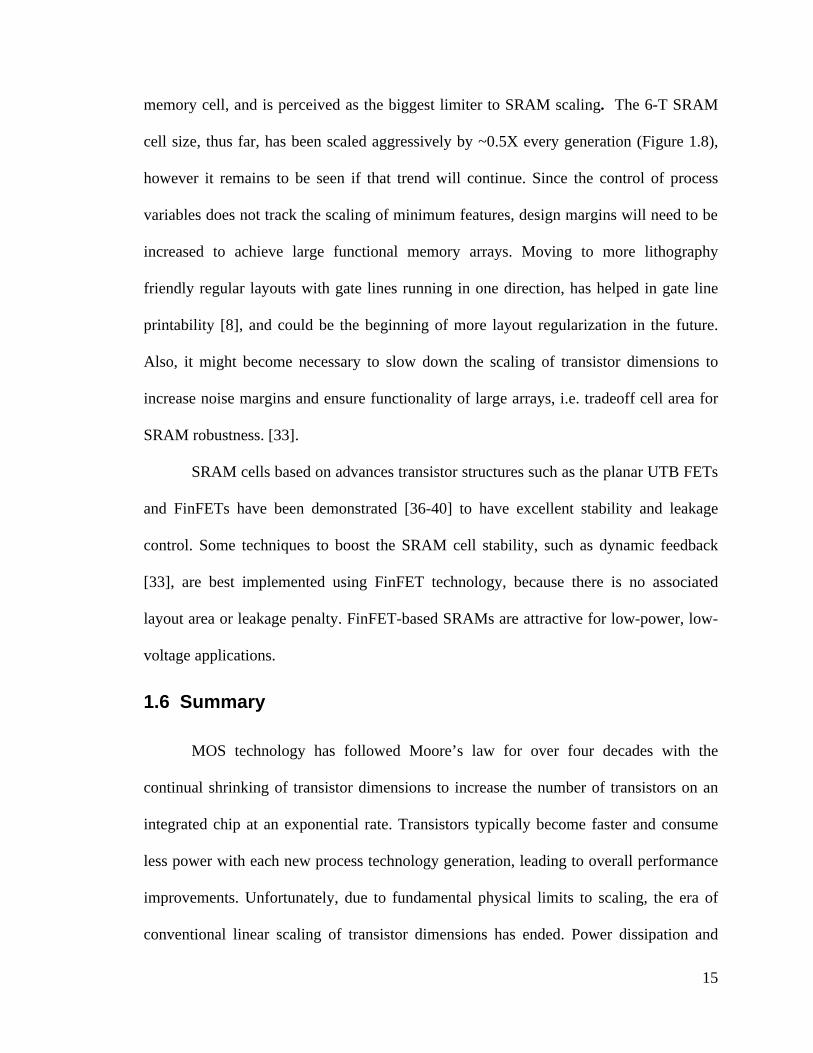
Figure 1.8: SRAM cell size has been scaling at ~0.5 x per generation [35], but it might
slow down due to lack of cell robustness caused by process induced variations.
The functionality and density of a memory array are its most important properties.
Functionality is guaranteed for large memory arrays by providing sufficiently large
design margins (to be able to be read without changing the state, to hold the state, to be
writable and to function within a specified timeframe), which are determined by device
sizing (channel widths and lengths), the supply voltage and, marginally, by the selection
of transistor threshold voltages. Increase in process-induced variations results in a
decrease in SRAM read and write margins, which prevents the stable operation of the
Page 15
15
memory cell, and is perceived as the biggest limiter to SRAM scaling. The 6-T SRAM
cell size, thus far, has been scaled aggressively by ~0.5X every generation (Figure 1.8),
however it remains to be seen if that trend will continue. Since the control of process
variables does not track the scaling of minimum features, design margins will need to be
increased to achieve large functional memory arrays. Moving to more lithography
friendly regular layouts with gate lines running in one direction, has helped in gate line
printability [8], and could be the beginning of more layout regularization in the future.
Also, it might become necessary to slow down the scaling of transistor dimensions to
increase noise margins and ensure functionality of large arrays, i.e. tradeoff cell area for
SRAM robustness. [33].
SRAM cells based on advances transistor structures such as the planar UTB FETs
and FinFETs have been demonstrated [36-40] to have excellent stability and leakage
control. Some techniques to boost the SRAM cell stability, such as dynamic feedback
[33], are best implemented using FinFET technology, because there is no associated
layout area or leakage penalty. FinFET-based SRAMs are attractive for low-power, low-
voltage applications.
1.6 Summary
MOS technology has followed Moore’s law for over four decades with the
continual shrinking of transistor dimensions to increase the number of transistors on an
integrated chip at an exponential rate. Transistors typically become faster and consume
less power with each new process technology generation, leading to overall performance
improvements. Unfortunately, due to fundamental physical limits to scaling, the era of
conventional linear scaling of transistor dimensions has ended. Power dissipation and
Page 16
16
process-induced variations are big issues for continued scaling of bulk-Si MOSFETs in
future generations. Improvements in transistor density, performance and power
consumption together with high yield will become harder to achieve. Advanced device
structures such as the UTB-FET and the FinFET offer improved performance and low
leakage. The back-gated FDSOI offers tunable performance and could be an attractive
solution for counteracting process-induced variations. These new transistor structures can
be seamlessly integrated into the CMOS design stream, making them attractive to extend
Si CMOS scaling. With power-aware design in the presence of variations (statistical
design) taking on a bigger role, extensive collaboration between circuit design, system
architects and semiconductor device and process engineers will be crucial to translate the
promises of these new device technologies into actual chip performance.
1.7 Research Objectives and Dissertation Outline
In this dissertation, the key benefits of thin-body MOSFETs over the conventional
planar bulk MOSFET are studied for future CMOS technologies. Through modeling and
device simulation, scaling issues and performance of nanoscale thin-body transistor
designs and their applications for improved circuit performance are evaluated.
In Chapter 2, transistor design optimization for the double-gate MOSFET is
outlined in order to maximize the drive current and minimize circuit delay while taking
into account parasitic resistance and capacitance effects. Based on this optimization, it is
shown that a double-gate MOSFET needs to have an effective channel length larger than
the physical gate length for scaling into the sub-10nm regime.
The gate delay versus energy consumption tradeoffs in double-gate versus back-
gated device designs are studied in Chapter 3. Adaptive VTH control in back-gated
Page 17
17
devices make them span a larger range in energy-delay space, making them attractive
single technology solutions for variable throughput applications ranging from high
performance to low power.
Chapter 4 quantifies the performance benefits of back-gated fully-depleted SOI
devices (BG-FDSOI). The scale length for the BG-FDSOI is derived as a function of
back-gate bias to account for the observed dependence of short channel effects on back-
gate bias. The scale length is used to guide device design so as to make the BG-FDSOI
close to FinFET in terms of performance while relaxing the body-thickness scaling
requirement through the use of back-gate bias. It is shown that back-gate biasing can be
used to partially reduce the impact of process variations.
Design considerations for FinFET based SRAM memory are discussed in Chapter
5. The tradeoffs in read margin, write margin, and cell area for various FinFET based
designs are presented. In addition, a new FinFET-cased SRAM cell with dynamic
feedback is shown to provide significant improvement in SRAM noise margin, without
area or leakage penalty. Also, a 4-T FinFET SRAM cell using dynamic feedback is
shown to be an attractive low cost, high-density memory solution.
Chapter 6 presents the process development involved in the fabrication of
FinFET-based SRAM with dynamic feedback. This involves the fabrication of double-
gate FinFETs and independent-gate FinFETs simultaneously and is achieved using
selective gate separation. The FinFET SRAM process has been transferred to other
industrial fabrication facilities, because dynamic feedback is a promising manufacturable
solution to extend SRAM scaling.
Page 18
18
An overall summary of this dissertation is presented in Chapter 7. Key research
contributions and suggestions for future research directions are highlighted.
1.8 References
[1] G. E. Moore, "Cramming more components onto integrated circuits," Electronics,
vol. 38, pp. 114 -- 117, 1965.
[2] G. E. Moore, "No exponential is forever: but "Forever" can be delayed!," presented
at Proceedings of IEEE International Solid-State Circuits Conference. San
Francisco, CA, 2003.
[3] E. J. Nowak, "Maintaining the benefits of CMOS scaling when scaling bogs down,"
IBM Journal of Research and Development, vol. 46, pp. 169-80, 2002.
[4] Z. H. Liu, C. Hu, J. H. Huang, T. Y. Chan, M. C. Jeng, P. K. Ko, and Y. C. Cheng,
"Threshold voltage model for deep-submicrometer MOSFETs," IEEE Transactions
on Electron Devices, vol. 40, pp. 86-95, 1993.
[5] H. Wakabayashi, S. Yamagami, N. Ikezawa, A. Ogura, M. Narihiro, K. Arai, Y.
Ochiai, K. Takeuchi, T. Yamamoto, and T. Mogami, "Sub-10-nm planar-bulk-
CMOS devices using lateral junction control," presented at IEEE International
Electron Devices Meeting 2003. Washington, DC, 2003.
[6] "International Technology Roadmap for Semiconductors, 2005 ed,"
http://www.itrs.net/Links/2005ITRS/Home2005.htm.
[7] "International Technology Roadmap for Semiconductors, 2003 ed,"
http://www.itrs.net/Links/2003ITRS/Home2003.htm.
[8] P. Bai, C. Auth, S. Balakrishnan, M. Bost, R. Brain, V. Chikarmane, R. Heussner,
M. Hussein, J. Hwang, D. Ingerly, R. James, J. Jeong, C. Kenyon, E. Lee, S. H.
Page 19
19
Lee, N. Lindert, M. Liu, Z. Ma, T. Marieb, A. Murthy, R. Nagisetty, S. Natarajan, J.
Neirynck, A. Ott, C. Parker, J. Sebastian, R. Shaheed, S. Sivakumar, J. Steigerwald,
S. Tyagi, C. Weber, B. Woolery, A. Yeoh, K. Zhang, and M. Bohr, "A 65nm logic
technology featuring 35nm gate lengths, enhanced channel strain, 8 Cu interconnect
layers, low-k ILD and 0.57 µm2 SRAM cell," presented at 2004 International
Electron Devices Meeting. San Francisco, CA, 2005.
[9] J. Butterbaugh and C. M. Osburn, "Frontend processes required for continued
CMOS scaling," Solid State Technology, 2006.
[10] A. Asenov, "Random dopant induced threshold voltage lowering and fluctuations in
sub-0.1 mm MOSFET's: A 3-D "Atomistic" simulation study," IEEE Transactions
on Electron Devices, vol. 45, pp. 2505-13, 1998.
[11] L. T. Su, J. B. Jacobs, J. E. Chung, and D. A. Antoniadis, "Short-channel effects in
deep-submicrometer SOI MOSFETS," presented at Proceedings of 1993 IEEE
International SOI Conference. Palm Springs, CA, 1993.
[12] H.-S. P. Wong, D. J. Frank, P. M. Solomon, C. H. J. Wann, and J. J. Welser,
"Nanoscale CMOS," Proceedings of the IEEE, vol. 87, pp. 537-70, 1999.
[13] L. Chang, Y. K. Choi, D. W. Ha, P. Ranade, S. Y. Xiong, J. Bokor, C. M. Hu, and
T. J. King, "Extremely scaled silicon nano-CMOS devices," Proceedings of the
IEEE, vol. 91, pp. 1860-1873, 2003.
[14] V. Subramanian, J. Kedzierski, N. Lindert, H. Tam, Y. Su, J. McHale, K. Cao, T. J.
King, J. Bokor, and C. Hu, "A bulk-Si-compatible ultrathin-body SOI technology
for sub-100 nm MOSFETs," presented at 1999 57th Annual Device Research
Conference Digest. Santa Barbara, CA, 1999.
Page 20
20
[15] Y.-K. Choi, K. Asano, N. Lindert, V. Subramanian, T.-J. King, J. Bokor, and C. Hu,
"Ultrathin-body SOI MOSFET for deep-sub-tenth micron era," IEEE Electron
Device Letters, vol. 21, pp. 254-5, 2000.
[16] J. Kedzierski, P. Xuan, V. Subramanian, J. Bokor, T.-J. King, C. Hu, and E.
Anderson, "A 20 nm gate-length ultra-thin body p-MOSFET with silicide
source/drain," presented at 5th Silicon Nanoelectronics Workshop. Honolulu, HI,
2000.
[17] Y. K. Choi, D. W. Ha, T. J. King, and C. M. Hu, "Nanoscale ultrathin body
PMOSFETs with raised selective germanium source/drain," IEEE Electron Device
Letters, vol. 22, pp. 447-448, 2001.
[18] Z. Krivokapic, W. Maszara, K. Achutan, P. King, J. Gray, M. Sidorow, E. Zhao, J.
Zhang, J. Chan, A. Marathe, and M. R. Lin, "Nickel silicide metal gate FDSOI
devices with improved gate oxide leakage," presented at IEEE International
Electron Devices Meeting. San Francisco, CA, 2002.
[19] J. Kedzierski, E. Nowak, T. Kanarsky, Y. Zhang, D. Boyd, R. Carruthers, C.
Cabral, R. Amos, C. Lavoie, R. Roy, J. Newbury, E. Sullivan, J. Benedict, P.
Saunders, K. Wong, D. Canaperi, M. Krishnan, K. L. Lee, B. A. Rainey, D. Fried,
P. Cottrell, H. S. Wong, M. Ieong, and W. Haensch, "Metal-gate FinFET and fully-
depleted SOI devices using total gate silicidation," presented at IEEE International
Electron Devices Meeting. San Francisco, CA, 2002.
[20] H.-S. P. Wong, K. K. Chan, and Y. Taur, "Self-aligned (top and bottom) double-
gate MOSFET with a 25 nm thick silicon channel," presented at International
Electron Devices Meeting. IEDM Technical Digest. Washington, DC, 1997.
Page 21
21
[21] D. Hisamoto, W.-C. Lee, J. Kedzierski, H. Takeuchi, K. Asano, C. Kuo, E.
Anderson, T.-J. King, J. Bokor, and C. Hu, "FinFET-a self-aligned double-gate
MOSFET scalable to 20 nm," IEEE Transactions on Electron Devices, vol. 47, pp.
2320-5, 2000.
[22] X. Huang, W.-C. Lee, C. Kuo, D. Hisamoto, L. Chang, J. Kedzierski, E. Anderson,
H. Takeuchi, Y.-K. Choi, K. Asano, V. Subramanian, T.-J. King, J. Bokor, and C.
Hu, "Sub 50-nm FinFET: PMOS," presented at International Electron Devices
Meeting 1999. Technical Digest. Washington, DC, 1999.
[23] N. Lindert, Y. K. Choi, L. Chang, E. Anderson, W. C. Lee, T. J. King, J. Bokor, and
C. Hu, "Quasi-planar FinFETs with selectively grown germanium raised
source/drain," presented at 2001 IEEE International SOI Conference. Proceedings.
Durango, CO, 2001.
[24] D. M. Fried, E. J. Nowak, J. Kedzierski, J. S. Duster, and K. T. Komegay, "A Fin-
type independent-double-gate NFET," presented at 61st Device Research
Conference. Salt Lake City, UT, 2003.
[25] L. Mathew, Y. Du, A.-Y. Thean, M. Sadd, A. Vandooren, C. Parker, T. Stephens,
R. Mora, R. Rai, M. Zavala, D. Sing, S. Kalpat, J. Hughes, R. Shimer, S. Jallepalli,
G. Workman, W. Zhang, J. G. Fossum, B. E. White, B. Y. Nguyen, and J. Mogab,
"CMOS Vertical Multiple Independent Gate Field Effect Transistor (MIGFET),"
presented at 2004 IEEE International SOI Conference. Charleston, SC, 2004.
[26] I. Y. Yang, C. Vieri, A. Chandrakasan, and D. A. Antoniadis, "Back gated CMOS
on SOIAS for dynamic threshold voltage control," presented at Proceedings of
International Electron Devices Meeting. Washington, DC, 1995.
Page 22
22
[27] T. Park, S. Choi, D. H. Lee, J. R. Yoo, B. C. Lee, J. Y. Kim, C. G. Lee, K. K. Chi,
S. H. Hong, S. J. Hynn, Y. G. Shin, J. N. Han, I. S. Park, U. I. Chung, J. T. Moon,
E. Yoon, and J. H. Lee, "Fabrication of body-tied FinFETs (Omega MOSFETs)
using bulk Si wafers," presented at 2003 Symposium on VLSI Technology. Digest
of Technical Papers. Kyoto, Japan. 10-12 June 2003, 2003.
[28] K. Okano, T. Izumida, H. Kawasaki, A. Kaneko, A. Yagishita, T. Kanemura, M.
Kondo, S. Ito, N. Aoki, K. Miyano, T. Ono, K. Yahashi, K. Iwade, T. Kubota, T.
Matsushita, I. Mizushima, S. Inaba, K. Ishimaru, K. Suguro, K. Eguchi, Y.
Tsunashima, and H. Ishiuchi, "Process Integration Technology and Device
Characteristics of CMOS FinFET on Bulk Silicon Substrate with sub-10 nm Fin
Width and 20 nm Gate Length," presented at IEEE International Electron Devices
Meeting, 2005. IEDM Technical Digest, Washington D.C., 2005.
[29] L. Chang, Y.-K. Choi, K. J., N. Lindert, P. Xuan, J. Bokor, C. Hu, and T.-J. King,
"Moore's law lives on," IEEE Circuits & Devices Magazine, vol. 19, pp. 35-42,
2003.
[30] S. Thompson, G. Sun, K. Wu, J. Lim, and T. Nishida, "Key differences for process-
induced uniaxial vs. substrate-induced biaxial stressed Si and Ge channel
MOSFETs," presented at 2004 International Electron Devices Meeting. San
Francisco, CA, 2005.
[31] K. Shin, T. Lauderdale, and T.-J. King, "Effect of tensile capping layer on 3-D
stress profiles in FinFET channels," presented at 63rd Device Research Conference
Digest, DRC '05., 2005.
Page 23
23
[32] K. Shin, C. O. Chui, and T.-J. King, "Dual Stress Capping Layer Enhancement
Study for Hybrid Orientation FinFET CMOS Technology," presented at IEEE
International Electron Devices Meeting (Washington D.C., USA), 2005.
[33] Z. Guo, S. Balasubramanian, R. Zlatanovici, T.-J. King, and B. Nikolic', "FinFET-
based SRAM design," presented at ISLPED '05. Proceedings of the 2005
International Symposium on Low Power Electronics and Design. San Diego, CA,
2005.
[34] A. Bhavnagarwala, S. Kosonocky, C. Radens, K. Stawiasz, R. Mann, and Q. Ye,
"Fluctuation Limits & Scaling Opportunities for CMOS SRAM Cells," presented at
International Electron Devices Meeting, Technical Digest, Washington DC, 2005.
[35] S.-M. Jung, H. Lim, W. Cho, H. Cho, C. Yeo, Y. Kang, D. Bae, J. Na, K. Kwak, B.
Choi, S. Kim, J. Jeong, Y. Chang, J. Jang, J. Kim, K. Kim, and B.-I. Ryu, "Highly
area efficient and cost effective double stacked S3 (stacked single-crystal Si)
peripheral CMOS SSTFT and SRAM cell technology for 512M bit density SRAM,"
presented at 2004 International Electron Devices Meeting. San Francisco, CA,
2005.
[36] E. J. Nowak, T. Ludwig, I. Aller, J. Kedzierski, M. Leong, B. Rainey, M.
Breitwisch, V. Gemhoefer, J. Keinert, and D. M. Fried, "Scaling beyond the 65 nm
node with FinFET-DGCMOS," presented at CICC Custom Integrated Circuits
Conference. San Jose, CA, 2003.
[37] T. Park, H. J. Cho, J. D. Choe, S. Y. Han, S. M. Jung, J. H. Jeong, B. Y. Nam, O. I.
Kwon, J. N. Han, H. S. Kang, M. C. Chae, G. S. Yeo, S. W. Lee, D. Y. Lee, D.
Park, K. Kim, E. Yoon, and J. H. Lee, "Static noise margin of the full DG-CMOS
Page 24
24
SRAM cell using bulk FinFETs (Omega MOSFETs)," presented at IEEE
International Electron Devices Meeting 2003. Washington, DC, 2003.
[38] R. V. Joshi, R. Q. Williams, E. Nowak, K. Kim, J. Beintner, T. Ludwig, I. Aller,
and C. Chuang, "FinFET SRAM for high-performance low-power applications,"
presented at Proceedings of the 34th European Solid-State Device Research
Conference. Leuven, Belgium. 21-23 Sept. 2004, 2004.
[39] P. Tai-Su, C. Hye Jin, C. Jeong Dong, H. Sang Yeon, P. Donggun, K. Kinam, E.
Yoon, and L. Jong-Ho, "Characteristics of the full CMOS SRAM cell using body-
tied TG MOSFETs (bulk FinFETs)," IEEE Transactions on Electron Devices, vol.
53, pp. 481-7, 2006.
[40] B. Doris, Y. H. Kim, B. P. Linder, M. Steen, V. Narayanan, D. Boyd, J. Rubino, L.
Chang, J. Sleight, A. Topol, E. Sikorski, L. Shi, L. Wong, K. Babich, Y. Zhang, P.
Kirsch, J. Newbury, J. F. Walker, R. Carruthers, C. D'Emic, P. Kozlowski, R.
Jammy, K. W. Guarini, and M. Leong, "High performance FDSOI CMOS
technology with metal gate and high-k," presented at 2005 Symposium on VLSI
Technology. Kyoto, Japan. Japan Soc. of Appl. Phys.. IEEE Electron Devices Soc.
14-16 June 2005, 2005.
Page 25
25
Chapter 2 : Circuit implications of scaling sub-25
nm double-gate MOSFETs
2.1 Introduction
Double gate MOSFETs (Figure 2.1) such as the FinFET are promising structures
to be scaled into the sub-25nm regime [1-4]. DG-MOSFETs usually are designed to have
very thin Si channel that is fully-depleted in order to cut-off sub-surface leakage paths,
thereby making them more scaleable. The use of lightly doped or undoped channels leads
to enhanced immunity to dopant fluctuation effects, smaller drain-to-body capacitance
and higher carrier mobility arising from a lower transverse electric field. With no doping
in the channel, metal gates with suitable work function are required to achieve reasonable
threshold voltages in fully-depleted devices. [5-8].
One of the challenges introduced by a thin silicon channel is the extremely high
parasitic series resistance and contact resistance at the source and drain (S/D) regions.
While parasitic resistance is a serious challenge in bulk devices [9, 10], the problem is
more severe in thin-body devices, and various process technologies have been proposed
to reduce it [11-13]. This chapter discusses device optimization methodology to identify
the device design tradeoffs involved in order to find the balance between good-control of
short channel effects (SCE) and minimizing external parasitic resistance. The tradeoffs
Page 26
26
between the various device parameters in determining the short-channel behavior can be
studied using the framework of the scale length [2, 14]. This is important from the
viewpoint of device scalability and is discussed in detail in Chapter 4.
Source Drain TSi
Gate
Gate
LG
TOX
External Contact
Figure 2.1: Schematic cross-section of the double-gate device structure use for
simulations. Graded source-drain junctions are used. The structure includes sidewall
spacers to capture the effect of parasitic capacitance. The gate work function is adjusted
to meet the IOFF specification.
2.2 Device Design Optimization
The DG-MOSFET device design optimization study has been carried out using
calibrated energy transport models in the device simulator, Medici [15] and cross-
checked with the quantum device simulator Nanomos 2.5 [16] for the case LG = 13 nm.
The parameters used in the simulations are tabulated in Table 2-1. The silicon body
thickness, TSi, needs to be around ~0.6 - 0.7 LG for adequate control of short channel
effects (SCE). The carrier energy relaxation times used in the hydrodynamic simulations
to account for transient velocity overshoot effects are adapted from [17].
Page 27
27
.
Parameter 45 nm node 32 nm node
LG (nm) 25 13
TOX (Å) 11 8
TSi (nm) 7 5
VDD(V) 0.7 0.5
Gate height (nm) 37.5 19.5
S-D gradient (nm/dec) 2.8 1.4
t relaxation (ps) 1.6 1.3
IOFF (µA/um) 0.3 1
Table 2-1: Summary of device parameters used in the simulations. The numbers used
here are essentially taken from the ITRS roadmap 2001 (with more conservative numbers
for TOX and IOFF). [18].
Commonly, device optimization has been carried out with the aim to maximize
the saturation drive current, ID,SAT, subject to an upper limit on the leakage current [5].
Using this approach, a 25nm gate length device has been optimized by changing the
source-drain separation in order to get the maximum drain current, ID,SAT (Figure 2.2).
The source-drain separation is related to the effective channel length of the device, LEFF,
and can be changed by adjusting the offset spacer thickness[19, 20].
The optimal source-drain (S-D) spacing is determined by a tradeoff between
short-channel effects (SCE) and the series resistance of the channel. When S-D
separation decreases, LEFF is reduced and the leakage current increases due to increased
worsened short channel effects. The S-D spacing is changed together with the metal gate
Page 28
28
work function, ΦM, to meet the constant IOFF specification. Therefore in a DIBL
dominated regime (small LEFF), a higher ΦM is needed to compensate for the leakage
increase due to degraded SCE. On the other hand, as the LEFF increases with a larger S-D
separation, the improvement in short channel effects due to reduced source/drain
coupling is offset by a large increase in parasitic extension resistance and poor gate
coupling between the channel and extensions, thereby degrading ID,SAT. Thus, the right
balance between the SCE and series resistance sets the optimal LEFF.
10 20 30 401.2
1.3
1.4
1.5
SCE dominated RS dominated
I d,sa
t (m
A/µ
m)
LEFF
or S-D separation (nm)
Figure 2.2: Dependence of the ID,SAT on the source to drain separation for LG=25 nm. The
optimal ID,SAT is set by the tradeoff between SCE and series resistance. LEFF is defined at
the position where the doping falls off to 2x1019 cm-3
Page 29
29
0.6 0.8 1.0 1.2 1.460
70
80
90
100 LG :
25 nm 13 nm
Su
bth
resh
old
Sw
ing
(m
V/d
ec)
LEFF
/LG, normalized S-D separation
Figure 2.3: Subthreshold swing variation with the S-D separation normalized w.r.t. LG.
The swing for shorter LG degrades due to increased source/drain coupling to the channel
resulting in worsened DIBL and sub-threshold swing.
1.0
1.1
1.2
1.3
1.4
1.5
0.7 0.9 1.1 1.3 1.5
LEFF/LG, normalized S-D separation
I D,S
AT
(A/u
m)
25 nm13 nm
LG :
Figure 2.4: The optimal LEFF needed is larger than LG for very small LG. With degraded
SCE, the optimal underlap between gate and source/drain regions needed is greater.
Page 30
30
Also, when the gate length is scaled from 25 nm to 13 nm, the short-channel
effects are degraded (Figure 2.3) if the TOX and TSi cannot be scaled proportionately to LG
due to gate leakage limitations. Therefore, the optimal S-D separation or LEFF for
maximizing ID,SAT in a scaled device with degraded SCE is expected to be larger. This is
verified in Figure 2.4. Thus, having an effective channel length that is larger than the
physical gate length (LEFF > LG) is probably necessary to continue scaling devices. The
trends hold true for PMOS devices as well.
In the above simulations the source/drain doping gradients were kept fixed as
shown in Table 2-1. In order to understand the effect of source/drain doping gradients on
device optimization, FinFETs with four different doping gradients were optimized to
have same IOFF and DIBL =100 mV/V, resulting in devices with the same VTH and SCE.
A device with a very graded profile would need thick gate sidewall spacers in practice to
reduce the S/D encroachment into the channel. The optimal doping profiles from
simulation are shown in Figure 2.5 and are all seen to intersect at a doping level of 2-3 x
1019 cm-3, which is the level at which LEFF is defined [20]. Alternatively, if the VTH and
SCE effects are the same in these devices, they ought to have the same LEFF. Therefore,
the doping level of 2-3 x 1019 cm-3 is an appropriate point from which to define LEFF,
consistent with [20].
This implies that different source-drain dopant activation technologies can be
used in conjunction with the appropriate spacer thickness to achieve the same LEFF. Steep
S/D junctions need thin spacers, while graded junctions need a correspondingly thicker
spacers.
Page 31
31
1E+15
1E+16
1E+17
1E+18
1E+19
1E+20
-20 -15 -10 -5 0 5 10 15 20
Distance from the channel center (nm)
S/D
Do
pin
g (
cm-3
)3 nm2 nm1 nm0.1 nm
LEFF
Figure 2.5: Equivalent source-drain doping profiles identified from Medici simulations
[15] of four different FinFET devices, all with the same IOFF and DIBL=100 mV/V.
These equivalent doping profiles all intersect at a doping level of 2-3 x 1019 cm-3,
implying that they all have the same LEFF. Steep junctions need thin gate sidewall
spacers, while graded junctions need a correspondingly thicker spacers to achieve the
same LEFF.
2.3 Effect of Parasitic Capacitances
This optimization for maximum ID,SAT, however, does not take into consideration
the role of parasitic capacitances and their impact on circuit performance. The total gate
capacitance is the sum of the gate oxide capacitance, the gate to S/D overlap capacitance
and the sidewall fringing capacitance [21].
σGaussian
Page 32
32
In order to separate the effect of the overlap capacitance from the sidewall
fringing effects, the capacitance simulations were run with a line gate, where the gate
height, TG, is set to zero. Therefore, CMIN, (CG @VGS=0), is related directly to the overlap
capacitance arising from the gate-to-source-drain overlap region. As the source and drain
separation increases, the overlap capacitance between the gate and the source-drain
regions decreases linearly (Figure 2.6). The CMAX, (CG @VGS=VDD), the gate capacitance
in strong inversion, is slightly smaller than COX (= εOX/TOX, equivalent oxide
capacitance), due to the increase in the electrical oxide thickness from quantum
mechanical effects and is independent of source/drain overlap.
0.0
0.2
0.4
0.6
0.8
1.0
18 22 26 30
S-D separation (nm)
CG (
fF/u
m)
Cox
Cmax
Cmin
LG = 25 nm
Figure 2.6: Variation of gate capacitance (CG) with the S-D separation (assuming a line
gate, TG = 0nm). CMAX is slightly smaller that COX because the quantum mechanical
charge centroid is shifted away from the oxide interface. CMIN (CG @VGS=0), decreases
almost linearly with the S-D separation due to reduced gate-to-source/drain overlap area.
Page 33
33
0.0
0.2
0.4
0.6
0.8
1.0
0.1 1 10 100
Gate height, TG (nm)
CG (
fF/u
m) Cox
Cmax
Cmin
LG = 25 nm
Figure 2.7: Variation of total gate capacitance (CG) with the gate height (TG). CMIN and
CMAX increase with gate height due to increased fringing fields and saturate at large TG.
The other component of the gate capacitance, the parasitic sidewall capacitance
through the gate sidewall spacer, is not affected by the source-drain overlap. This
component increases as the height of the gate is increased and saturates at large values of
the gate height (Figure 2.7). While a smaller gate height is good to achieve a smaller
capacitance, the height of the gate electrode is often determined by the need to keep the
sheet resistance of the gate within bounds, and to ensure that the channel is protected
from the S/D implants.
2.4 Circuit Simulations
To investigate the effect of parasitic capacitance on circuit performance, mixed-
mode simulations of inverter FO-4 buffer chain were carried out in Medici [15]. The
parasitic source/drain capacitance for a thin body transistor is very small, so it is expected
that the optimal fan-out using the method of logical effort for minimal delay would be
Page 34
34
closer to 3 [22]. However, a smaller effective fan-out per stage increases the number of
driving stages and the total layout area, and the sensitivity of delay to fan-out near the
optimal fan-out is small, so the fan-out factor of 4 is still used in this study.
CLOAD
Delay measured across 2nd stage
1st stage shapes input signal 3rd stage provides
appropriate loading
VDD
VDD
VDD
1x 4x 16x
Figure 2.8: Schematic of FO-4 inverter mixed-mode simulation setup to measure the
stage delay. The chain consists of 3 stages, the first stage corrects the input slope, the
propagation delay is measured across the second stage and the last stage has a capacitive
load equal to 4x of its input capacitance to present the appropriate Miller capacitance
The dependence of the FO-4 inverter delay on the source-drain spacing was
investigated. The optimal spacing was found to be larger than that expected from
maximizing drive current (Figure 2.9). This is because as the gate-to-S/D overlap region
becomes smaller, its parasitic contribution to the total gate capacitance decreases.
Therefore, in increasing the S/D spacing beyond the optimal value for maximum ID,SAT,
(from Figure 2.2) the capacitance reduction is more significant than the reduction in
ID,SAT, which results in a overall reduced delay. However, when the source-drain spacing
Page 35
35
becomes even larger i.e. as the gate to S/D underlap increases, the series resistance starts
to dominate and the delay goes back up. The optimal spacing corresponding to minimal
delay can result in dynamic power savings as well, because the parasitic part of the total
switching capacitance is lowered significantly.
1.0
1.1
1.2
0.8 1 1.2 1.4
LEFF/LG, normalized S-D spacing
I D,S
AT
(mA
/um
)
2.1
2.2
2.3
2.4
FO
-4 d
elay
(p
s)
Idsat
FO-4 delay
ID,SAT
Figure 2.9: Dependence of the ID,SAT and FO-4 delay on the normalized source to drain
separation for LG = 13 nm. The optimal separation from the delay perspective is clearly
larger than that for maximum ID,SAT, i.e. LEFF>LG
2.5 Device Optimization under constant DIBL constraint
Device optimization thus far has been carried out under constant IOFF, with LEFF as
the only design variable. As LEFF is made longer, the DIBL gets better monotonically. In
reality, constant VTH (sets leakage) and constant DIBL are both constraints that need to
be satisfied in maximizing performance. This aspect is addressed in greater detail in
Chapter 4 on back-gated FDSOI design. In this section, a 100mV/V DIBL constraint is
Page 36
36
additionally imposed, and the design optimization is briefly addressed below. Here Tsi is
the additional physical parameter that is varied together with LEFF to optimize device
performance under DIBL constraints.
Optimal design
LEFF (nm) TSi(nm)
I D,S
AT
(mA
/um
) Constant DIBL contour
Figure 2.10: Dependence of ID,SAT on TSi and LEFF for DG-MOSFET with LG = 13 nm,
EOT = 6 Å, ρC = 10-8 Ω cm2. As TSi increases, SCE are degraded, and LEFF needs to be
longer in order to meet the constant DIBL constraint, as shown by the constant DIBL
contour. The optimal ID,SAT shows a weak dependence on TSi, decreasing with thinner TSi
due to higher series resistance.
For each TSi, the LEFF optimization is carried out as described in Section 2.2 in
order to identify the optimal ID,SAT and is shown by maximum ID,SAT contour in Figure
2.10. When TSi increases, SCE are degraded, and LEFF needs to be longer in order to meet
the constant DIBL constraint, as shown by the constant DIBL contour in Figure 2.10. The
intersection point between the maximum ID,SAT contour and the constant DIBL contour
Page 37
37
corresponds to the optimal device under DIBL constraints from the viewpoint of
maximizing ON-current. A similar study can be carried out to identify optimal delay
point under SCE constraints.
2.6 Conclusions
When optimizing DG-MOSFET for maximum drive current, ID,SAT, under constant
leakage constraints, it is seen that the effective channel length, LEFF, is an important
design parameter. The optimal S-D separation is determined from the tradeoffs between
short-channel effects and parasitic series resistance. Nanoscale devices may have to be
designed with gate underlapped source/drain regions to meet the SCE requirements and
optimize their performance. Also, the optimal underlap for maximizing drive current,
ID,SAT, is seen to be larger for smaller gate length devices. It is clear that optimizing
devices with circuit performance considerations is important. The impact of parasitic
capacitances on the performance of DG-MOSFETs has been investigated. The optimal
LEFF for minimizing circuit delay has been found to be larger than that needed to
maximize transistor drive current, due to smaller parasitic overlap capacitance.
2.7 References
[1] H. S. P. Wong, Y. Taur, and D. J. Frank, "Discrete random dopant distribution
effects in nanometer-scale MOSFETs," Microelectronics Reliability, vol. 38, pp.
1447-1456, 1998.
[2] D. J. Frank, Y. Taur, and H. S. Wong, "Generalized scale length for two-
dimensional effects in MOSFETs," IEEE Electron Device Letters, vol. 19, pp. 385-
7, 1998.
Page 38
38
[3] L. L. Chang, Y. K. Choi, J. Kedzierski, N. Lindert, P. Q. Xuan, J. Bokor, C. M. Hu,
and T. J. King, "Moore's law lives on - Ultra-thin body SOI and FinFET CMOS
transistors look to continue Moore's law for many years to come," Ieee Circuits &
Devices, vol. 19, pp. 35-42, 2003.
[4] Y.-K. Choi, N. Lindert, P. Xuan, S. Tang, D. Ha, E. Anderson, T.-J. King, J. Bokor,
and C. Hu, "Sub-20 nm CMOS FinFET technologies," presented at International
Electron Devices Meeting. Technical Digest. Washington, DC, 2001.
[5] L. Chang, S. Tang, K. Tsu-Jae, J. Bokor, and H. Chenming, "Gate length scaling
and threshold voltage control of double-gate MOSFETs," presented at International
Electron Devices Meeting. Technical Digest. IEDM. San Francisco, CA, 2000.
[6] P. Ranade, R. Lin, Q. Lu, Y. C. Yeo, H. Takeuchi, T. J. King, and C. Hu,
"Molybdenum gate electrode technology for deep sub-micron CMOS generations,"
presented at Gate Stack and Silicide Issues in Silicon Processing II. Symposium.
San Francisco, CA, 2002.
[7] I. Polishchuk, P. Ranade, T. J. King, and C. Hu, "Dual work function CMOS gate
technology based on metal interdiffusion," presented at Gate Stack and Silicide
Issues in Silicon Processing II. Symposium. San Francisco, CA, 2002.
[8] D. W. Ha, P. Ranade, Y. K. Choi, J. S. Lee, T. J. King, and C. M. Hu,
"Molybdenum gate work function engineering for ultra-thin-body silicon-on-
insulator (UTB SOI) MOSFETs," Japanese Journal of Applied Physics Part 1-
Regular Papers Short Notes & Review Papers, vol. 42, pp. 1979-1982, 2003.
[9] S. Thompson, P. Packan, T. Ghani, M. Stettler, M. Alavi, I. Post, S. Tyagi, S.
Ahmed, S. Yang, and M. Bohr, "Source/drain extension scaling for 0.1 um and
Page 39
39
below channel length MOSFETs," presented at 1998 Symposium on VLSI
Technology Digest of Technical Papers. Honolulu, HI, 1998.
[10] J. Yuan, P. M. Zeitzoff, and J. C. S. Woo, "Source/drain parasitic resistance role
and electrical coupling effect in sub 50 nm MOSFET design," presented at 32nd
European Solid State Device Research Conference. Firenze, Italy. 24-26 Sept. 2002,
2002.
[11] Y. K. Choi, D. W. Ha, T. J. King, and C. M. Hu, "Nanoscale ultrathin body
PMOSFETs with raised selective germanium source/drain," Ieee Electron Device
Letters, vol. 22, pp. 447-448, 2001.
[12] Y. Chunshan, V. W. C. Chan, and P. C. H. Chan, "Low S/D resistance FDSOI
MOSFETs using polysilicon and CMP," presented at Proceedings 2001 IEEE Hong
Kong Electron Devices Meeting. Hong Kong, China. IEEE Electron Devices Soc..
Dept. Electron. & Inf. Eng. Hong Kong Polytech. Univ. 30 June 2001, 2001.
[13] Z. Krivokapic, W. Maszara, F. Arasnia, E. Paton, Y. Kim, L. Washington, E. Zhao,
J. Chan, J. Zhang, A. Marathe, and M. R. Lin, "High performance 25 nm FDSOI
devices with extremely thin silicon channel," presented at 2003 Symposium on
VLSI Technology. Digest of Technical Papers. Kyoto, Japan. 10-12 June 2003,
2003.
[14] K. Suzuki, T. Tanaka, Y. Tosaka, H. Horie, and Y. Arimoto, "Scaling theory for
double-gate SOI MOSFET's," IEEE Transactions on Electron Devices, vol. 40, pp.
2326-9, 1993.
[15] "Medici v. 2002.4," Synopsys Inc.
[16] "Nanomos, v 2.5," http://nanohub.purdue.edu.
Page 40
40
[17] M. Y. Chang, D. W. Dyke, C. C. C. Leung, and P. A. Childs, "High-energy
electron-electron interactions in silicon and their effect on hot carrier energy
distributions," Journal of Applied Physics, vol. 82, pp. 2974-9, 1997.
[18] "International Technology Roadmap for Semiconductors," 2001.
[19] Y. Taur and T. H. Ning, Fundamentals of Modern VLSI Devices: Cambridge
University Press, 1998.
[20] Y. Taur, Y.-J. Mii, R. Logan, and H.-S. Wong, "On "effective channel length" in
0.1-um MOSFETs," IEEE Electron Device Letters, vol. 16, pp. 136-8, 1995.
[21] J. M. Rabaey, A. Chandrakasan, and B. Nikolic´, Digital Integrated Circuits, 2 ed:
Prentice Hall, 2002.
[22] I. Sutherland, R. F. Sproull, and D. Harris, Logical Effort: Designing Fast CMOS
Circuits: Morgan Kaufmann Publishers, 1999.
Page 41
41
Chapter 3 : Energy-Delay Optimization of Multi-
Gate FETs in the sub-25nm era
3.1 Introduction
There are primarily two types of power dissipation in a CMOS digital integrated
circuit: dynamic and static. The dynamic power arises from the useful work done in
switching between logic states during digital computation. Dynamic power is
proportional to CVDD2f, where C is the capacitive load being switched, VDD is the supply
voltage, and f is the clock frequency. The dynamic power dissipation is directly related to
the rate of computation, so it can be adjusted to meet power budgets by adjusting the
frequency of operation. Supply voltage scaling can also be used to adjust the dynamic
power dissipation [1].
Static power, on the other hand, is associated with the holding of logic states i.e.
when the circuit is idle. This power is due to leakage mechanisms such as sub-threshold
leakage or gate leakage within the transistors in the circuit, and is wasteful because it
does not contribute to computation [1]. Leakage is unavoidable in modern CMOS
technologies, and actually increases exponentially with scaling and is perceived as a
major roadblock to scaling [2]. Today’s microprocessors have thus entered power-limited
Page 42
42
scaling where performance alone is not critical; rather performance under a power budget
is the metric of relevance [3].
Power dissipation becomes a primary design constraint with further CMOS
scaling, requiring circuit designs to be optimized considering both energy and delay. The
effectiveness of heat removal system from hot spots poses limits on the power density,
and impacts system cost and maximum attainable performance. Power constraints are
even more stringent in mobile processor designs in which long battery life is desirable.
The goal of a processor design, therefore, is to achieve the maximum operating frequency
while meeting the power density constraint.
For high-performance chips, the high subthreshold leakage current must be within
bounds to keep chip static power dissipation within acceptable limits. One common
approach is multi-VTH technology, where low VTH high-performance MOSFETs, are used
only in critical paths to meet delay requirements and higher VTH and larger EOT devices
with lower leakage currents are used everywhere else to minimize the overall power
dissipation without sacrificing performance. To achieve optimal energy vs. delay (E-D)
performance [4], multiple transistor designs are needed to cater to various application
areas. Other circuit/architectural techniques used to curtail static power dissipation
include the use of sleep transistors to cut off access to power/ground rails or other
techniques to power down circuit blocks [5].
Another potential technique used in bulk-Si MOSFET technology to tune the VTH
of NMOS and PMOS transistors separately is adaptive body biasing (ABB). The VTH of a
transistor can be controlled to a limited extent by using ABB, by applying a finite body-
to-source voltage. By modulating the VTH, the overall leakage and frequency for a die can
Page 43
43
be controlled to some extent. Reverse body biasing (RBB) has been employed to reduce
the standby leakage power dissipation, and the application of forward body bias (FBB) in
active mode increases the frequency of operation, but it increases the leakage power as
well. FBB has the desirable result of reducing the depletion thickness of the channel,
thereby improving the short-channel effects (SCE) of a bulk-Si MOSFET, and improves
the overall sensitivity to parametric variations. For the same reason, RBB increases the
sensitivity to process variations due to worsened SCE. In extremely scaled transistors, the
body effect is degraded due to worse short channel effects, and so adaptive body biasing
to reduce leakage is not effective [6, 7]. Implementing ABB in bulk-Si technology
requires a triple-well technology, which may not always be available.
For a multi-gate FET, adaptive threshold control, implemented through back-gate
biasing, can be used in conjunction with dynamic voltage scaling (DVS) to minimize
power dissipation in circuits and has been used in this study to achieve energy-delay
optimality [8-11]. The goal of this combined VDD and VTH scaling scheme is to achieve
the optimal combination of frequency and power, i.e. identify the minimum energy
required to operate at a certain target frequency.
With parallelism, achieved through the use multiple cores, becoming more
important, the emphasis on transistor performance is reducing and that on lower leakage
transistors with minimal variations is increasing. In scaled technologies, achieving the
target VTH through process control alone is getting harder and the degree of process
variations is getting larger. Dynamically tunable VTH technologies provide a post-
manufacturing electrical knob to fine tune a chip back to within the specifications and
Page 44
44
thereby fill this gap between the target and achievable VTH and are expected to become
more important in the future.
Conventional UTB or FDSOI MOSFETs are built on thick BOX and therefore
exhibit little or no effect on VTH from the application of back-gate bias. However, when
the BOX thickness is scaled down, the back-gate coupling to the channel increases and
the VTH change with back-gate bias can be used to modulate MOSFET performance. This
chapter presents the design of energy-delay optimized back-gated thin-body SOI
MOSFETs, (BG-FETs), and uses back-gate biasing to control the leakage power
dissipation. It is demonstrated here that BG-FETs exhibit power savings over double-gate
MOSFETs that increase with scaling into the sub-10 nm gate length regime. [12]
3.2 Adaptive VTH in FDSOI MOSFETs
In this section, we quantify the circuit level benefits of enhancement mode (ENH)
thin-body double gate (DG) and back-gated (BG) MOSFETs.
FG
BG S/D Contact
LG
TGATE
TSi
LSP
TOX
TBOX
Distance
Do
pin
g (c
m-3
)
LEFF1020
1014
Source Drain
2x101
9
Figure 3.1 - Cross-sectional schematic of BG FETs studied. The effective channel length,
LEFF, for the BG-FET is defined as the separation between the points where doping falls
off to 2x1019 cm-3.
Page 45
45
32 nm node 22nm node
DG-FET
Device parameters BG ENH
HPa LPb BG-ENH
LG (nm) 13 9
LSP (nm) 13 9
TOX (Å) (EOT) 6 5
TBOX(Å) 63 11.5 11.5 47
TSi (nm) 5 8.2 8.2 3
TGATE (nm) 19.5 19.5 19.5 13.5
NBODY (cm-3) 2 x 10¹⁶ 2 x 10¹⁶ 2 x 10¹⁶
ΦG(eV) 4.4 4.45 4.6 4.33
VDD (V) 0.6 0.6 0.6 0.5
S-D σGaussian (nm) 2.0 2.0 2.0 1.4
ρC, (Ω-cm2) 5x10⁻⁹ 5x10⁻⁹ 5x10⁻⁹
LEFF (nm) 20.2 15.6 15.6 12
Ioff, active (µA/µm) 1 1 0.01 3
ION (µA/um) 575 665 398 629
I SLEEP (nA/µm)c 10 1000 10 66
Table 3-1: Summary of the MOSFET design parameters used. - HPa refers to high
performance and LP b refers to low power. The LEFF for the MOSFET is defined as
distance between points where the doping concentration falls to 2x1019 cm-3. c The sleep
state standby leakage current, ISLEEP, is evaluated at VBG = -VDD.
Page 46
46
DG-FET and BG-FET device simulations were carried out in the Taurus-Device
simulator using drift-diffusion transport and the 1-D Schrödinger equation [13]. (See
Figure 3.1 and Table 3-1).
3.3 Transistor Design Optimization
The DG-FETs and BG-FETs were each optimized to achieve maximum ION at
constant active-state leakage, IOFF = 10-6 A/µm, and DIBL of 100 mV/V. This was
achieved by co-optimizing TSi, TBOX, S-D separation to change LEFF, and using gate
workfunction tuning to achieve the target IOFF, at constant TOX using the design-of-
experiments (DOE) methodology, similar to that described in Chapter 2 [14]. Two
versions of the DG-FET are also included in the study: a low VTH, high-performance
(HP) device and a higher VTH, low-power (LP) device. (See Table 3-1.) The only
difference between these two devices is the VTH, with the LP device having a 100x lower
leakage as compared to the HP device, achieved through a gate workfunction shift. These
two versions of the DG-FETs would be needed for a multi-VTH technology to control the
overall power dissipation as discussed earlier. Note that LEFF must be larger than the
physical gate length LG to achieve good short channel effects in sub-15nm devices [15]
(Table 3-1).
BG-FETs, have a thicker TBOX, and therefore need to have a thinner body than
DG-FETs to have the same degree of short channel effect control. In this section, the
front- and back-gate workfunctions are assumed to be equal, resulting in a negligible
transverse electric field in the channel. This pushes the active state leakage path to
position of the weakest gate control, i.e. the back oxide/channel interface. However, in
the sleep state, a reverse bias can applied to the back-gate to reduce the leakage of these
Page 47
47
devices. The scalability of the BG-FET can be improved if reverse back-gate biasing can
be used even in the active mode (together with a front-gate with a lower workfunction to
compensate for the accompanying VTH shift) to setup a high electric field in the channel
and is described in chapter 4.
A thinner TBOX provides higher VTH sensitivity to VBG. However, an ultra-thin
TBOX also has increased quantum-mechanical direct tunneling between the back-gate and
the channel near the drain edge, thereby increasing the BG–leakage current in the sleep
mode. Another disadvantage is worsened sub-threshold slope and device
transconductance, gM, due to the capacitive division of the channel potential between the
front gate and the back-gate causing degraded transistor performance. In addition, at large
reverse back-gate bias values, the back channel is biased into accumulation and the VTH
sensitivity to back-biasing becomes quite weak. At that point, the maximum reverse bias
is limited by the back-gate induced band-band tunneling (BTBT) between the back-
channel accumulation layer and the reverse-biased drain. The TBOX was chosen in this
work in such a way that the back-side BTBT leakage limit is still not reached at
maximum back bias (limited to -VDD for the n-channel MOSFET) and the direct
tunneling leakage through the back-oxide is small (50-100× lower) compared to IOFF.
The back-gate effect to modulate VTH in back-gated FDSOI devices can be
retained with scaling if the TBOX can be scaled as well (Figure 3.2). The TBOX needs to be
about ~5x –10x of the TOX to have a good tradeoff of VTH tunability without having to
apply a very large VBG and to limit degradation of device turn-on characteristics.
Page 48
48
0
0.1
0.2
-0.6 -0.4 -0.2 0
VBG (V)
dVT
H (V
)
13 nm
9 nm
Figure 3.2 - The BG-FET devices show good sensitivity to VBG that is retained with
scaling, if the TBOX is scaled as well. (ref. Table 3-1)
3.4 Comparison of DG-FETs and BG-FETs
BG-FETs and DG-FETs are compared to study the short channel behavior, ON-
state performance and the immunity to process-induced variations. Figure 3.2 shows that
the BG-FET design can be optimized to have a large back-gate effect, and therefore can
be put into deep sleep mode, making it attractive for low power applications. Simulations
of the BG- FETs were carried out with LG = 9nm and 13nm, and the effectiveness of the
back-gate control on VTH is still retained at short LG. The BG-FETs are optimized in
order to achieve a sleep state current of 10-8 A/µm at VBG = -VDD. Increasing the back-
gate effect to reduce the sleep state current comes at the expense of ION. From Figure 3.3,
it can be seen that the BG-FETs devices have ION intermediate to those for the HP and LP
DG-FETs. In order to limit saturation current degradation arising from the back-gate
effect, a thicker TBOX is desirable.
Page 49
49
0
200
400
600
0.0 0.3 0.6
VDS(V)
I DS (
A/u
m)
0
200
400
600
0.0 0.3 0.6
VDS(V)I D
S(A
/um
)
Simulation
Model
0
200
400
600
0.0 0.3 0.6
VDS(V)
I DS(A
/um
)
(a) HP DG-FET (b) LP DG-FET (c) BG–FET
Figure 3.3 - Drain characteristics of the FETs used in the study. (a-c) The simulation data
from Taurus [13] (points) was fitted to an empirical model (Eq 3-1), shown by solid lines.
0E+00
2E-04
4E-04
6E-04
0.2 0.4 0.6 0.8 1
VGS [V]
I DS [
A]
Simulation
Model
dVTH = 300mV/V
1E-09
1E-08
1E-07
1E-06
0.0 0.2 0.4 0.6VDS(V)
I OF
F (A
/um
)
VBG=0 V
VBG=-0.6 V
Figure 3.4 (a) Change in the IDS with back-gate biasing is captured through (b) IOFF vs.
VDS @VBG. The leakage of the BG devices matches that of the HP DG-FET at zero back
bias, and at VBG = -VDD match that of the LP DG-FET.
Page 50
50
( )
−
+−−
=A
DS
CDS
DSTHGSDSDLIN V
VLEV
VVVKVI 1
5.02
( )
−
+−−
=A
DS
CTHGS
THGSDSAT V
VLEVV
VVKI 1
2
Eq. 3-1
( )THGSC
THGScDSAT VVLE
VVLEV
−+−
=
A semi-empirical device model (Eq. 3-1) based on a subset of BSIM3 model equations
can fit the simulated drain current characteristics, IDS-VDS data of HP, LP DG-FETs and
BG-FETs (Figure 3.3). It also captures the VTH shift from back-gate biasing and captures
its effect on ON-state and OFF-state currents (Figure 3.4). Also, mobility enhancement
parameters and the effect of parameter variations can be modeled to create Spectre
AHDL models for DC simulation to estimate gate delay and power dissipation.
-0.1
0.0
5 10 15 20 25
LG (nm)
dV
th (V
)
FinFET
BG-FET
High Perf.
-0.1
0.0
5 10 15 20 25
LG (nm)
Low Power
Figure 3.5 - The BG-FET devices show similar VTH-rolloff behavior to the DG-FET
devices. The low power and high-performance devices show similar VTH-roll off.
In comparing short-channel effects, VTH roll-off (
Page 51
51
Figure 3.5) and the sensitivity of VTH to TSi variations (Figure 3.6) for the BG-
FET and the FinFET devices are similar. The DG-FET shows slightly better roll-off and
lower TSi sensitivity, because it has the thickest Si body.
-0.05
0
0.05
-10% 0% 10%
TSi Variation
dV
TH (
V)
BG-FET
FinFET
High Perf.
-0.05
0
0.05
-10% 0% 10%TSi Variation
Low Power
Figure 3.6 - The BG-FET and the DG-FET devices show similar sensitivity to variations
in TSi for both HP and LP designs.
The BG-FET has slightly larger inversion gate capacitance as compared to the
DG-FET (Figure 3.7) due to its increased carrier confinement due to the applied back-
gate bias resulting in a quantum-mechanical charge centroid location that is closer to the
gate oxide interface. The BG-FET needs to have a slightly longer LEFF as compared to the
DG-FET to achieve the same SCE, resulting in a reduced overlap capacitance.
Page 52
52
0.0
0.2
0.4
0.6
0 0.2 0.4 0.6VFG (V)
CG
ATE
(fF/
mm
)DG-FET
BG- FET
LG = 13 nm
Figure 3.7 - The gate capacitance is similar for BG-FET and DG-FET devices, thus, the
intrinsic delay, tp0, scales with ION.
3.5 Circuit level benefits of BG-FETs
Adaptive supply- and threshold-voltage scaling can be used to minimize energy
dissipation as delay requirements of a circuit change. Deeply scaled bulk-Si MOSFETs
have limited VTH tuning range due to reduced body effect and reduced VDD/VTH ratios [6,
7]. The VTH of DG-FET devices cannot be dynamically changed. The VTH tunability of
deeply scaled BG devices makes them attractive for achieving minimal energy over a
wide range of target frequencies.
Adaptive body biasing can be used to set the optimum VTH for each die so as to
compensate for variations in chip performance or power dissipation [6, 7]. The VTH of the
NMOS/PMOS devices in each die is therefore controlled not only by gate workfunction
and channel length engineering but also by the application of the appropriate forward or
Page 53
53
reverse back-gate bias. Dies that are too slow and fail to meet the performance target
need to be forward biased, thereby increasing the die operating frequency and the overall
die leakage, whereas those that leak excessively have to be reverse biased, reducing the
operating frequency as well. The goal of the ABB is to find the optimum PMOS/NMOS
VTH combination that maximizes the die frequency while meeting the leakage constraint.
Dynamic voltage scaling (DVS) [16] can been used to reduce the dynamic power
dissipation because of the quadratic dependence of switching power on VDD. As VDD is
scaled, the device currents are degraded due to a reduced gate overdrive, VGS-VTH,
leading to slower switching speeds. This is the only power saving technique that can be
applied to DG-FETs such as the FinFET, which have no external VTH control capability.
This interdependence between dynamic power and switching speeds can be broken by
using a combination of DVS and ABB. VDD can be scaled to save switching power and
the VTH can be lowered correspondingly to maintain enough gate overdrive to retain the
switching speed. However, reducing the VTH increase the leakage current of the
transistors significantly. Therefore, there exists a clear tradeoff between the static power
dissipation (from lowering VTH) and the active power (from lowering VDD) for a given
application, leading to the existence of an optimal VDD and VTH combination that requires
the lowest energy to perform a given task [4, 17].
Figure 3.8 demonstrates an example system, where adaptive VDD and VTH control
of BG-FETs achieves wider energy scalability spanning the range of both HP/LP DG-
FETs. While the highest performance achievable by BG-FETs is lower than that of HP
DG-FETs, the minimum energy approaches that of the LP DG-FETs when the
Page 54
54
computational throughput is reduced significantly. Thus the BG-FET spans a wide range
of E-D space and is the energy optimal device for intermediate frequencies. [12]
0
2
4
6
8
0 2 4 6 8Frequency (GHz)
En
erg
y (n
J)
HP DGLP DGBG-FET
Figure 3.8 - Dynamic voltage scaling of DG-FETs and BG FETs at LG = 13nm. With
back-gate bias adjusted as voltage is scaled, the BG-FETs are able to achieve higher
performance than the low-power DG-FET and lower energy than the HP DG-FET.
Active leakage control [18] implemented with BG devices allows a circuit to
benefit from the low sleep-state leakage while still having performance that is determined
by the active-state ION. The energy penalty for placing a BG device in the sleep state is
the switched capacitance of the back gate, and it can be done in a single cycle. For a bulk-
Si MOSFET, switching a large well capacitance incurs a significant energy and delay
penalty. Since the benefits of the BG-FET device (Figure 3.2) going into a deeper sleep is
retained with scaling into the sub-10nm regime, it is well suited for leakage control in
future systems. In our simulations the maximum applied negative back bias was limited
to -VDD; in practical systems it can be made more negative.
Page 55
55
Circuit Parameters Value
Logic depth 375 CV/I
Gate area 2.4 mm2
Activity 10%
% Core sleep 30%
Table 3-2: Example system @ LG = 13nm
0.1
1.0
10.0
100.0
1E+02 1E+03 1E+04
LD x tp0 (ps)
Po
wer
(W
)
HP-FinLP-FinBG-FET
microprocessor DSP embedded
Figure 3.9: Minimum power envelope with changing logic depth in the example system
(Table 3-2). The envelope represents the minimum power achievable through a
combination of voltage scaling and back-gate biasing to adjust VTH.
Figure 3.9 illustrates E-D trade-offs with varying logic depths in an example
system implemented with both DG-FETs and BG-FETs. BG-FET implementations make
use of adaptive threshold control and active leakage control in addition to VDD adjustment
to achieve a wider range of optimality. The minimum power envelope for the BG-FETs
Page 56
56
lies in between that of the HP and LP FinFETs. Both Figure 3.8 and Figure 3.9 illustrate
the capability of the BG-FETs to achieve delays similar to a HP DG-FET, and attain the
low power of LP DG-FETs at low operating frequencies.
A multi-VTH DG-FET technology with more that three VTH values can potentially
outperform BG-FETs, but the benefit of BG-FET technology is in providing a single
technology solution to meet different target applications with different throughput
requirements.
3.6 Conclusions
Power dissipation of scaled high performance ICs will be controlled by utilizing
more than one type of transistor together with device, design and architectural techniques.
This chapter presents the design of energy-delay optimized BG-FETs, and discusses the
effectiveness of back-gate biasing to control the leakage current. It is demonstrated that
BG-FETs exhibit power savings benefits over double-gate MOSFETs that increase with
scaling into the sub-10 nm regime. Energy vs. delay (E-D) optimization shows that BG-
FETs can span a wide range in E-D space, making it possible to have a single-device
solution to meet high performance and low power needs through adaptive supply and
threshold voltage biasing.
Page 57
57
3.7 References
[1] J. M. Rabaey, A. Chandrakasan, and B. Nikolic´, Digital Integrated Circuits, 2 ed:
Prentice Hall, 2002.
[2] "International Technology Roadmap for Semiconductors, 2005 ed,"
http://www.itrs.net/Links/2005ITRS/Home2005.htm.
[3] B. Nikolic', L. Chang, and T.-J. King, "Performance of Deeply-Scaled, Power-
Constrained Circuits," presented at International Conference on Solid State Devices
and Materials, Tokyo, 2003.
[4] R. W. Brodersen, M. A. Horowitz, D. Markovic, B. Nikolic', and V. Stojanovic,
"Methods for true power minimization," presented at 2002 IEEE/ACM
International Conference on Computer Aided Design (ICCAD). San Jose, CA,
2002.
[5] J. T. Kao and A. P. Chandrakasan, "Dual-threshold voltage techniques for low-
power digital circuits," IEEE Journal of Solid-State Circuits, vol. 35, pp. 1009-18,
2000.
[6] A. Keshavarzi, S. Ma, S. Narendra, B. Bloechel, K. Mistry, T. Ghani, S. Borkar,
and V. De, "Effectiveness of reverse body bias for leakage control in scaled dual Vt
CMOS ICs," presented at ISLPED'01: Proceedings of the 2001 International
Symposium on Low Power Electronics and Design. Huntington Beach, CA, 2001.
[7] J. W. Tschanz, J. T. Kao, S. G. Narendra, R. Nair, D. A. Antoniadis, A. P.
Chandrakasan, and V. De, "Adaptive body bias for reducing impacts of die-to-die
and within-die parameter variations on microprocessor frequency and leakage,"
Page 58
58
presented at 2002 IEEE International Solid-State Circuits Conference. Digest of
Technical Papers. San Francisco, CA, 2002.
[8] D. Liu and C. Svensson, "Trading speed for low power by choice of supply and
threshold voltages," IEEE Journal of Solid-State Circuits, vol. 28, pp. 10-17, 1993.
[9] T. Kuroda, K. Suzuki, S. Mita, T. Fujita, F. Yamane, F. Sano, A. Chiba, Y.
Watanabe, K. Matsuda, T. Maeda, T. Sakurai, and T. Furuyama, "Variable supply-
voltage scheme for low-power high-speed CMOS digital design," presented at 1997
Custom Integrated Circuits Conference. Santa Clara, CA, 1998.
[10] K. Nose and T. Sakurai, "Optimization of VDD and VTH for low-power and high-
speed applications," presented at Proceedings of ASP-DAC2000: Asia and South
Pacific Design Automation Conference 2000. Yokohama, Japan. IEEE Circuits &
Syst. Soc.. ACM SIGDA. IEICE of Japan. IPSJ (Inf. Process. Soc. Japan). 25-28
Jan. 2000, 2000.
[11] T. Chen and S. Naffziger, "Comparison of adaptive body bias (ABB) and adaptive
supply voltage (ASV) for improving delay and leakage under the presence of
process variation," IEEE Transactions on Very Large Scale Integration (VLSI)
Systems, vol. 11, pp. 888-99, 2003.
[12] S. Balasubramanian, J. L. Garrett, V. Vidya, B. Nikolic', and T. J. King, "Energy-
delay optimization of thin-body MOSFETs for the sub-15 nm regime," presented at
2004 IEEE International SOI Conference. Charleston, SC, 2004.
[13] "Taurus-Device, v. 2002.4," Synopsys Inc., 2002.
Page 59
59
[14] D. J. Frank, Y. Taur, and H. S. Wong, "Generalized scale length for two-
dimensional effects in MOSFETs," IEEE Electron Device Letters, vol. 19, pp. 385-
7, 1998.
[15] S. Balasubramanian, L. Chang, B. Nikolic', and T.-J. King, "Circuit-performance
implications for double-gate MOSFET scaling below 25 nm," presented at Silicon
Nanoelectronics Workshop, Kyoto, Japan, 2003.
[16] T. D. Burd and R. W. Brodersen, "Energy efficient CMOS microprocessor design,"
presented at Proceedings of the Twenty-Eighth Annual Hawaii International
Conference on System Sciences. Wailea, HI, 1995.
[17] V. Stojanovic, D. Markovic, B. Nikolic, M. A. Horowitz, and R. W. Brodersen,
"Energy-delay tradeoffs in combinational logic using gate sizing and supply voltage
optimization," presented at ESSCIRC 2002. Proceedings of the 28th European
Solid-State Circuit Conference. Firenze, Italy. 24-26 Sept. 2002, 2002.
[18] J. W. Tschanz, S. G. Narendra, Y. Ye, B. A. Bloechel, S. Borkar, and V. De,
"Dynamic sleep transistor and body bias for active leakage power control of
microprocessors," IEEE Journal of Solid-State Circuits, vol. 38, pp. 1838-45, 2003.
Page 60
60
Chapter 4 : Design of back-gated FDSOI devices
4.1 Introduction
Thin-body (fully depleted) SOI MOSFETs are promising to continue CMOS
technology scaling in the sub 45-nm regime, because they provide better control of short-
channel effects (SCE) as compared with the classic bulk-Si MOSFET. For good
electrostatic integrity, i.e. the lateral dimensions of the device need to be much longer
than the vertical dimensions of the device. The degree of SCE control is often
characterized by the scale length, λ, which is a measure of the effective thickness of the
MOSFET channel in the direction transverse to current flow.
A new scale length formula to capture two-dimensional (2-D) electrostatic effects
in independently gated FDSOI MOSFETs has been derived in this chapter. The scale
length accounts for the effective location of the conduction path of sub-threshold leakage
and thereby captures the back-gate bias dependence of short channel effects and sub-
threshold swing. In order to account for quantum-mechanical effects in thin Si channels,
a quantum-corrected, bias-dependent effective conduction path model is proposed. The
scale length model can then be used to model the SCE in back-gated FDSOI devices
(BG-FDSOI) devices and guide device design to improve their performance. It is shown
that reverse back-gate biasing reduces the scale length by pushing the leakage path closer
to the front channel surface, thereby improving control of short-channel effects. We
Page 61
61
therefore propose the use of reverse back-gate biasing for active-mode operation to relax
the body thinness requirement for FDSOI MOSFETs, to make it comparable to that for
the FinFET, i.e. TSi ~ (2/3) LG. The performance of such a BG-FDSOI MOSFET with a
relaxed body thickness requirement can therefore approach that of a FinFET of the same
body thickness, with comparable SCE. Also, BG biasing can be used to compensate for
VTH shifts due to process-induced variations.
4.2 Background - Scale length of Thin-Body MOSFETs
The potential inside the channel depletion region of a bulk-Si MOSFET is
controlled by the four terminals of the device: gate, body contact, source and drain. The
control of the channel from the source/drain regions is undesirable and should be
minimized. Two-dimensional effects can be characterized by the control of the channel
potential by the source/drain regions relative to the gate and substrate or back-gate
contact. When the horizontal dimension, i.e., the channel length, is at least twice as long
as the vertical dimension, (a combination of TOX and the depletion width), XDEP, the
device behaves like a long-channel MOSFET, with its threshold voltage insensitive to
channel length and drain bias. For channel lengths shorter than that, the 2D effect
becomes significant, and the minimum surface potential (ΦS), which determines the
threshold voltage, is increasingly controlled by the drain than by the gate. For good
control of SCE effects, the scale length, λ, which describes how thin the MOSFET is in
the vertical dimension, needs to be small, i.e. LEFF or LG >> λ. A large scale length, λ,
indicates strong SCEs that degrade device behavior.
A general 2-D scale length formula has been derived by Frank et.al. [1] for thin-
body devices, but the solution form is implicit and hard to use except for the lowest order
Page 62
62
term. An approximate, but closed form scale length for double-gate (DG) thin-body
MOSFETs was proposed by Suzuki et al. [2], assuming that leakage current flows along
the center of the body. Chiang [3] generalized the scale length formula in [4] to account
for leakage current flowing along an effective conduction path located at a distance dEFF
from the center of the body, or the most probable leakage path [5]. Avci [6] proposed a
scale length formula from [2] for a back-gated (BG) MOSFET, in which the front and
back gates are independently biased, assuming that leakage flows along the front channel
surface. In this chapter, we generalize the scale length formula for a lightly doped BG
MOSFET to be a function of dEFF, which depends on the back-gate bias and back oxide
thickness.
4.3 Derivation of Quantum-Corrected Effective Conduction Path
The scale length is extracted by formulating the 2-D Poisson’s equation along the
effective conduction path, dEFF, which is the weighted `centre of gravity' of subthreshold
current. When a reverse bias applied on the back-gate, the channel charge is quite small
arising from the lack of signification depletion and inversion charge, leading to linear
band bending in the channel or a constant transverse electric field, e. The scale length
model derived here captures changes in SCE through the bias-dependence of dEFF. In
BG-FDSOI MOSFETs with a thin silicon body, the derivation of a quantum-corrected
effective conduction path becomes important and is shown below.
Page 63
63
Front Back
- TSi/2 TSi/2
Energy
0
eeTSi
dEFF
E(1)
y
Figure 4.1: The effective conduction path, dEFF, corresponds to the charge of the electron
wavefunction. The vertical field across the channel sets up a trapezoidal quantum well.
As the confining electric field increases, the conduction path gets closer to the interface.
For an infinite rectangular quantum well with an applied electric field, ε, the exact
wavefunction are based on the Airy functions. This form of the solution is hard to
manipulate mathematically to derive other dependencies and the principle of variations
can be used to derive a simpler, but approximate solution.
If the exact wavefunction solution to the Schrödinger equation cannot be found,
then the variational method can be used start with any normalized wavefunction that
satisfies the boundary conditions. For that initial guess, say Ψ, and it turns out that the
expectation value of the Hamiltonian, H, i.e. the Eigen energy, for the guessed
wavefunction will always be greater than the actual ground state energy. Or in other
words, if the approximate wavefunction is a function of a number of parameters, varying
these parameters until the expectation value of H is a minimum, minimizes the error for
that form of the wavefunction. The result is an upper limit for the ground state energy of
Page 64
64
the system, which is likely to be close to actual ground state energy if the trial vector
resembles the eigenvector. A variational wave function solution of the following form
has been used for the case of the triangular quantum well. [7].
( ) ( )
−=Ψ
SiSi Tx
Tx
Nx βπ
β expcos (Eq. 4-1)
where ß is the variational parameter, and N(ß) is the normalization constant. The ground
state energy Eigen values can then be written based on the Hamiltonian, H= H0 + eey as,
( ) ( ) ( )
−
++++= β
πββ
βη
πβ
β coth21
21
1EE 222
21 (Eq. 4-2)
where 2
2(1)
8 E
Si*Tm
h= , the ground state energy for the rectangular quantum well, and the
dimensionless energy, ( )1ETe Siε
η = .The optimal value of ß is obtained by minimizing E(ß)
w.r.t ß, i.e. by setting dE/dß = 0,
( ) ( )( )
03
csc2
22222
442
21 =
+
+−+==
πββ
πββ
ηπ
ββ
hEddE
(Eq. 4-3)
The analytical solution to this equation is hard to find, and the system was solved
numerically [7]. But the limits of this function are known, as η → 0, ηπ
β
−= 1
6
2
, and
as η → ∞, ( ) 3126 ηπβ = . It is to be noted that the optimal value of ß depends uniquely
only on η, resulting in an universal relation. The real solution to the cubic equation (Eq.
5-4) can be solved analytically and is verified to match the numerical solution to (Eq 5-
3).
Page 65
65
2
3
2 61
6πβ
πβ
η +
−
= (Eq. 4-4)
Knowing ß, we can derive dEFF as the expectation value of the position operator, |y>
( ) ( )
( ) ( )( )
−
++==
∫
∫
−
− βπβ
ββ
ψψ
ψψcoth
21
21
Tdyyy
dyyyyd
22Si2/Tsi
2/Tsi
*
2/Tsi
2/Tsi
*
EFF (Eq. 4-5)
- 1/2
1/2
-0.8 -0.4 0.0 0.4 0.8
Channel Electric Field, ECH (MV/cm)
Nor
mal
ized
con
duct
ion
path
, dE
FF/
TS
i Tsi = 5nm
Tsi = 15nmQM deff model
TSi/2
Front Interface
TOX = 10 ÅTBOX = 50 Å
Back Interface
-TSi/2
Figure 4.2: The effective conduction path, dEFF, changes with the vertical channel electric
field. As the confining field increases, the conduction path gets closer to the interface,
thereby improving gate control and reducing SCEs. A thicker back-oxide degrades ?BG,
but this can be negated by pushing the carriers closer to the interface with a larger vertical
field.
The effective conduction path, dEFF, is the expectation value of the charge
centroid of the electron wavefunction as measured from the center of the body. Figure 4.2
Page 66
66
shows the change in the dEFF as a function of the applied electric field, e, and as expected,
QM effects prevent the dEFF from reaching all the way to the interfaces. The sensitivity of
dEFF to channel electric field becomes smaller with TSi scaling, indicating that a thinner
silicon body behave more like a rectangular well and the effectiveness of a vertical
electric field in pushing the carriers to the surface is diminished. Thus, QM effects are
expected to reduce the benefits of back-gate biasing in extremely scaled devices.
4.4 Scale Length Derivation for BG-FDSOI devices
BOX
Gate1
Source Drain
Gate2
(0,0) xy
VBG
VFG
VDSTBOX
TOX
TSi
dEFF
IOFF
Figure 4.3 Schematic cross-sectional view of a back-gated (BG) FDSOI MOSFET. The
front and back gates can be independently biased and may have different work function
values. Note that the y-axis is along the vertical direction with its origin located at the
center of the silicon body.
This scale length model attempts to quantify the short-channel behavior of a fully
depleted transistor with back-gate biasing. The origin of the coordinate system used is set
Page 67
67
at the source end along the center of the Si body (Figure 4.3). The label dEFF refers to the
effective conduction path, measured from the center of the body. Also, the source
potential is used as the reference point, i.e. VS=0. The following assumptions and
approximations are made to set up the problem:
1. Since only the short-channel effects are solved here, the MOSFET is biased in the
subthreshold region, and the full depletion approximation is used inside the fully
depleted body.
2. Ideal abrupt source/drain junctions are assumed, so that the boundaries between
the source/drain and channel do not move with bias.
3. In a FDSOI device, the body is so thin that vertical doping engineering becomes
impractical. Therefore, undoped channel is assumed.
4. Also, metallic gates with appropriate workfunctions are assumed in order to set
the correct VTH and to ignore gate depletion effects that change the EOT
5. The electrical field in the gate dielectric and thin BOX is assumed to be strictly
vertical. The 2D effect of the gate dielectric and back-oxide will be modeled using
a quasi-2D approximation similar to they way it is modeled in [8].
The 2-D Poisson's equation for the potential F (x, y) in a BG FDSOI MOSFET is
Si
A2
2
2
2 qNy
)y,x(x
)y,x(ε
ΦΦ=
∂∂
+∂
∂ (Eq. 4-6)
For constant channel doping, the solution to the potential profile can be given by a
parabolic profile
( ) ( ) ( ) 2321 yxCyxCxC)y,x( ++=Φ (Eq. 4-7)
The electric field continuity at the front and back surface can be written in terms of their
Page 68
68
respective potentials F f (x) = F (x,-TSi/2) and F b(x) = F (x, TSi/2) as follows,
( )fbgbeff,gb
BOX
eff,gbb
Si
OX
2/T
VV V where,T
Vx
dy)y,x(
Si
−=−
−=∂ Φ
εεΦ
(Eq. 4-8)
( )fbgfeff,gf
OX
eff,gff
Si
OX
2/T
VV V where,T
Vx
dy)y,x(
Si
−=−
=∂
−
Φ
εεΦ
(Eq. 4-9)
Using Eq. 5-8 and 5-9 to express the solution coefficients in Eq. 5-7 in terms of F f (x)
and F b(x),
( ) ( ) ( ) ( )( ) ( )( )( )BOXOXSi
fgfBOXbgbOXox
Si
fb2 TT2
xVTxVTT
xxxC
εΦΦεΦΦ −−−
=−
= (Eq. 4-10)
( ) ( )( ) ( )( )( )BOXOXSiSi
fgfBOXbgbOXox3 TTT2
xVTxVTxC
ε
ΦΦε −+−= (Eq. 4-11)
( ) ( ) ( ) ( )2
Si3
fb1 2
TxC
2
xxxC
−
+=
ΦΦ (Eq. 4-12)
The back surface potential, F b(x) can be rewritten in terms of the front surface potential
F f(x) as follows
( )( ) ( )
+
++−
=
SiBOXOXSi
OX
fBOXOXSi
SiOXBOXgfOXgbOXSi
b
T2
TT
xT2
TTTVTV
2T
xεε
ΦεεεΦ (Eq. 4-13)
Based on eqs. (5-10) – (5-13), the coefficients C1(x), C2(x), and C3(x) can be expressed in
terms of F f(x) alone. With the coefficients known, the potential along the effective
conduction path F deff(x) = F (x,dEFF) , can then be written in terms of F f(x). This can then
be inverted to express F f(x) in terms of F deff(x) as follows,
Page 69
69
( )( ) ( )
−
++
+
−+
−
+
++
+−
+
−+
−
=
OXeffSi
effSi
BOXeffSi
effSi
Siox
2eff
2Si
Si2ox
2SiBOXOXSi
deffBOXSiSioxSiOXSigbOXSiox
2
effSi
gfeffSi
effSi
BOXSiox2eff
2Si
Si2ox
f
Td2
Td
2T3
Td2
Td
2T3
d2
TTTTT2
xT2TTTVTd2
T
Vd2
Td
2T3
Td2
TT
x
εε
εε
Φεεεεε
εεε
Φ (Eq. 4-14)
Equation (5-7) can now be written in terms of F deff(x). Using Eqs. (5-10)-(5-14) and
differentiating F (x,y), we get
2
deff2
2
2
x
)x(
x)y,x(
∂
∂=
∂∂ ΦΦ
(Eq. 4-15)
( )
( )
−
++
+
−+
−
+
+
+−+
+
−−
=∂
∂
OXeffSi
effSi
BOXeffSi
effSi
oxSi
2eff
2Si
Si2ox
2SiBOXOXSi
OXSieffSi
oxdeffgb
BOXSieffSi
oxdeffgf
OX
2
2
Td2
Td
2T3
Td2
Td
2T3
d2
TTTTT2
Td2
TV
Td2
TV
2
y)y,x(
εε
εε
εεΦ
εεΦ
ε
Φ (Eq. 4-16)
The Poisson’s equation (Eq 5-6) can now be rewritten in the following form:
( ) ( )Si
A2f
deffgf
2b
deffgb
2
deff2 qNVV
x
)y,x(
ελ
Φ
λ
ΦΦ=
−+
−+
∂
∂ (Eq. 4-17)
with,2bg
2b
2f
111λλλ
=+ (Eq. 4-18)
where ?f and ?b refer to the scale lengths characterizing front and back gate control
respectively. ?BG is the overall scale length of independent-gate FDSOI device which
depends on dEFF and is given by,
Page 70
70
( )( )SiBOXOXoxSiox
OXeffSi
effSi
BOXeffSi
effSi
oxSi
2eff
2Si
Si2ox
2SiBOXOXSi
BG TTT2
Td2
Td
2T3
Td2
Td
2T3
d2
TTTTT2
εεε
εε
εε
λ++
−
++
+
−+
−
+
= (Eq. 4-19)
0
5
10
15
-7.5 -5 -2.5 0 2.5 5 7.5
Effective Conduction path, d EFF (nm)
Sca
le L
eng
th, ?
BG
(n
m)
10 A30 A100 A3000 A
TBOX TSi = 15 nmTOX = 10 Å
Front Interface
Back Interface
FinFET
BG-FDSOI
Constant ?BG
Figure 4.4: Dependence of scale length ?BG on dEFF. As the effective location of the
leakage path moves closer to the front interface (i.e. as dEFF approaches -TSi/2), ?BG
decreases and hence the scalability of the FDSOI MOSFET improves. A thicker TBOX
degrades ?BG, but this can be compensated by pushing the leakage path closer to the front
interface by applying a larger channel electric field ECH (Figure 4.2).
Eq. 5-19 expresses the scale length of the BG-FDSOI device, λBG, as a function of
the various device parameters TOX, TSi, TBOX and the applied back-gate bias through dEFF.
From Eq. 5-19 it is evident that improvements in the scale length, ?BG, can be achieved by
Page 71
71
pushing the carriers closer to either the front or the back-gate dielectric interface.
However, in order to achieve good transistor drive current characteristics, it is necessary
to have TBOX > TOX so that the coupling from the front gate to the channel is good. For the
same reason, a greater improvement in ?BG is achieved by pushing the carriers to the front
gate dielectric rather than the back-gate dielectric interface as seen in Figure 4.4.
4.5 Implications of Scale length on BG-FDSOI Device Design
Eq 5-19 can be depicted in the form of a constant-scale-length surface as shown in
Figure 4.5. It can be seen that TOX, TBOX, and TSi can be traded off against each other in
achieving a target scale length. It is clear that in order to scale BG-FDSOI from LG =
25nm down to 13nm, the TOX, TBOX, and TSi have to be made correspondingly smaller as
well. The application of a reverse back-gate bias pushes out the contour to thicker values
of TOX, TBOX, and TSi, thereby increasing the scalability of the FDSOI MOSFET. This
improvement in scale length explains the experimental observations that SCE control is
improved with reverse-back-gate biasing [9]. Reverse back-gate biasing can therefore be
employed as a way to control SCE through its effects on dEFF in addition to adjusting
VTH, and can potentially be used to relax the body thinness requirement for FDSOI
MOSFETs, making them more manufacturable.
Page 72
72
TO
X (
nm
)
LG = 13nm
VBG = -1V
VBG = 0V
VBG = -1V
VBG = 0V
LG = 25nm
TBOX (nm) TSi (nm)
Figure 4.5: 3-D plot of constant scale length contours versus TOX, TSi, and TBOX for back-
gated FDSOI MOSFET’s for two different back-gate voltages at the 65nm and 32nm
technology nodes. Clearly as the gate length is scaled, smaller TOX, TSi, and TBOX are
needed, but these can be relaxed by applying a reverse back-gate bias, which improves
the scalability of the device by pushing out the constant scale length surface.
Page 73
73
0.5
1
1.5
2
2.5
3
3 6 9 12TSi (nm)
TO
X (n
m)
5 / 0
5 / -0.5
20 / 020 / -0.5
—— FinFET TBOX(nm)/ Ey(MV/cm) (BG-FDSOI)
λBG = 6 nm
Figure 4.6: 2-D plot of constant scale length curves showing the tradeoff between TOX
and TSi, for a DG MOSFET (TBOX = TOX) and for a back-gated FDSOI MOSFET, for two
different TBOX thicknesses. When a reverse back-gate bias is applied (Ey = 0.5 MV/cm),
TOX, TSi, and TBOX requirements can be relaxed as is evident in the pushed out constant-
λBG curve (filled symbols – applied bias) to larger values of TOX and TSi,. A thicker buried
oxide (5nm - > 20 nm) degrades ?BG, but this can be compensated by applying a larger
channel field ECH
Page 74
74
-0.3
-0.2
-0.1
0.0
20 40 60 80 100
LG (nm)
dVTH
(V)
Vbg = -0.7V
Vbg = 0V
SCE model
60 mV lower VTH roll-off with applied reverse bias
λBG based
Figure 4.7: VTH roll-off plot comparing Taurus-Device simulations and SCE model based
on the scale length (Eq. 5-19). The plot shows the benefit of reverse back-gate biasing to
improve SCE. For specified values of TOX, TBOX, TSi, and leakage (IOFF = 200 nA/um,
achieved by gate workfunction adjustment), reverse back gate biasing with VBG = -0.7V
improves VTH roll-off by pushing the leakage path closer to the front interface, as
captured by the dEFF formulation.
Threshold-voltage roll-off and drain-induced barrier lowering can be deduced
from the scale length using the same formulation used by Liu et al. [8, 10]. It should be
noted that, although a thin BOX helps to improve SCE in FDSOI devices by effectively
shielding the drain electric field, it can degrade MOSFET sub-threshold swing and hence
ON-state current, making the scale length just one of multiple criteria to consider in
device design.
Page 75
75
4.6 Relaxed Body-Thickness Scaling in BG-FDSOI MOSFETs
Short-channel effects (SCE) are well suppressed in a FDSOI MOSFET with
undoped channel/body when the body thickness TSi is less than or equal to one-third of
the gate length LG. However, as LG is scaled to below 20nm in sub-45nm CMOS
technologies, TSi must be scaled to below 5nm, so that parasitic series resistance (Rseries)
and threshold voltage (VTH) sensitivity to TSi variation become serious issues. In contrast,
the double-gate (DG) MOSFET structure (e.g. the FinFET) avoids these issues because
the body thinness requirement is less stringent: TSi ~ (2/3) LG. However, DG transistor
structures such as the vertical FinFET are more challenging to manufacture than the
planar FDSOI MOSFET structure.
Back-gate (BG) biasing has been shown to be effective for adjusting VTH in
FDSOI MOSFETs with thin buried oxide (BOX) [11]. Reverse BG biasing suppresses
SCE [9, 11-15] in contrast to reverse body biasing of bulk-Si MOSFETs which worsens
SCE. This is because the application of a reverse back-gate bias VBG increases the
vertical electric field in the channel ECH, pushing the off-state leakage path closer to the
front channel surface. (Note that the magnitude of VBG required to achieve the desired
ECH will increase with increasing buried oxide thickness TBOX.) We therefore propose the
use of reverse back-gate biasing for active-mode operation to relax the body thinness
requirement for FDSOI MOSFETs, to make it comparable to that for the FinFET, i.e. TSi
~ (2/3) LG. The performance of such a BG-FDSOI MOSFET with a relaxed body
thickness requirement can therefore approach that of a FinFET of the same body
thickness, with comparable SCE.
Page 76
76
4.7 BG-FDSOI MOSFET Design Considerations
Device simulations were carried out using Taurus-Device [16] with drift-diffusion
models, the 1-dimensional Schrödinger Equation to account for quantum confinement,
and surface mobility models to account for electric-field dependent degradation in
mobility. In order to realistically include the effects of parasitic series resistance and
capacitance, transistor structures with silicided raised-source/drain regions were
simulated (Figure 4.8).
Raised S/D
Sidewall Contact
Source
Gate
TSi
LG
LSP
Gate
Drain Source
S/D silicide
Source
Raised S/D Contact
Source
Drain
BOX
Back Gate
TSi
LG
LSP Front Gate
TBOX
S/D silicide
(a)
(b)
LCONT
LCONT
TR/SD
TR/SD
Figure 4.8: Cross-sectional schematic of a) double-gate MOSFET structure b) BG-
FDSOI MOSFET structure used for device simulations. The device parameters used are
LG = 13nm, TSi = 8nm, TOX = 8Å, LCONT = 40nm, TRS/D = 5nm, TSILI = 10nm [17]. For the
BG-FDSOI MOSFET, the back gate is p+ poly-Si for an n-channel device and n+ poly-Si
for a p-channel device.
TSILI
TSILI
Page 77
77
The aim of this simulation study was to take advantage of the improvement in
scalability with reverse BG biasing to design a BG-FDSOI device with the same off-state
leakage current, SCE, gate oxide thickness TOX, and TSi as that of a DG-MOSFET and to
compare their performance, delay, and immunity to variations.
-3
-2.5
-2
-1.5
-1
-0.5
00 20 40 60 80 100
TBOX (A)
VB
G,M
AX
(V)
Figure 4.9 : Maximum applicable reverse back-gate bias before the onset of BGIDL, i.e.
band-to-band tunneling between the accumulation layer and the reverse-biased drain in
BG-FDSOI NMOSFETs.
As |VBG| is increased, the back channel surface is biased into accumulation, and
band-to-band tunneling (BTBT) occurs at the back channel surface between the
accumulation layer and drain. This phenomenon can be considered as back-gate induced
drain leakage (BGIDL), and it places an upper limit on |VBG|. This limit increases with
TBOX, since larger |VBG| is needed to achieve the same degree of energy-band bending in
the channel to induce BGIDL for thicker TBOX (Figure 4.9). It should be noted that BTBT
Page 78
78
occurs at a smaller value of |ECH| in PMOS devices than in NMOS devices, therefore the
maximum |VBG| that can be applied in PMOS BG-FDSOI devices is smaller [18].
For device design optimization, |VBG| was chosen to be the maximum allowable
for TBOX. (From BGIDL considerations, |ECH| should not exceed 0.5 MV/cm.) Since
|VBG| is limited, it is difficult for the BG-FDSOI MOSFET to achieve the same degree of
SCE control as a FinFET with the same TSi. Therefore, the BG-FDSOI MOSFET must
have a slightly larger electrical channel length LEFF; this can be achieved in practice by
increasing the offset spacer thickness (LSP). The work function of the front (switching)
gate electrode and LEFF were each adjusted so that the BG-FDSOI and FinFET designs
meet the leakage current (IOFF) specification (300 nA/µm) and the SCE control
requirements. In order to achieve the desired VTH and maximize the effectiveness of BG
biasing, it is best to use gates with asymmetric work-function (ΦM), e.g. low-ΦM front
gate and high-ΦM back gate, for an n-channel BG-FDSOI MOSFET.
Using this approach, n-channel and p-channel BG-FDSOI MOSFET designs for
LG = 13nm, TSi = 8nm, and TOX = 8Å (same as for FinFET devices) were optimized by
adjusting TBOX and LEFF to achieve maximum on-state drain current, ID,SAT, while meeting
SCE and IOFF specifications. The design optimization involves a tradeoff between SCE,
parasitic series resistance, and the degree of back-gate coupling. Figure 4.10 shows that
the BG-FDSOI MOSFET can achieve an on-state current (per micron effective channel
width) that is ~6% smaller than the FinFET, for a given off-state current (100nA/µm),
while its gate capacitance is ~5% larger than that of the FinFET. The gate capacitance is
increased because the built-in electric filed pushes the inversion charge centroid closer to
the interface, thereby reducing the capacitance equivalent thickness. The on-current is
Page 79
79
degraded in comparison to the FinFET due to the increased carrier scattering from the
increased transverse electric field.
0.0
0.2
0.4
0.6
0.8
0.0 0.3 0.6 0.9
VGS (V)
Gat
e C
apac
itanc
e (f
F/um
)
0.0
0.2
0.4
0.6
0.8
1.0
Dra
in C
urre
nt (m
A/u
m)
FinFET
BG-FDSOI
TSi = 8nmTOX = 8A
Figure 4.10: Simulated drain current characteristics and gate capacitance of BG-FDSOI
vs. double-gate MOSFET (FinFET), for LG = 13nm, TOX = 8Å, TSi = 8nm. TBOX = 4nm
for the FDSOI device. The BG-FDOI device has marginally higher gate capacitance and
~6% lower on-state current (for a fixed IOFF = 300nA/µm).
Figure 4.11 shows that the optimal TBOX for maximizing ID,SAT is 25 Å for a 13 nm
LG BG-FDSOI MOSFET. As the TBOX thickness is increased, SCE are worsened, so LEFF
needs to be longer, at a cost to ID,SAT. When TBOX is very thin, SCE are well controlled,
but the strong back-gate coupling degrades ID,SAT due to the capacitive division of the
channel potential between the front- and back-gate potentials.
Page 80
80
0.8
0.9
1.0
10 30 50 70 90
TBOX (A)
I D,S
AT
(mA
/um
)
2.5
3.0
3.5
4.0
4.5
FO
-3 d
elay
(p
s)
Id,sat
FO-3 delay
ID,SAT
Figure 4.11: Dependence of ID,SAT and FO-3 delay on TBOX for LG = 13 nm. The optimal
TBOX for minimal delay is clearly larger than that for maximum ID,SAT.
4.8 Effect of Parasitic Capacitances
A disadvantage of thin TBOX is significant BG and source/drain parasitic
capacitances. To assess the impact of this parasitic capacitance on circuit performance,
mixed-mode simulations of an inverter FO-3 buffer chain were carried out. It is seen
from Figure 4.11 that the optimal TBOX for minimizing stage delay is ~40Å, which is
larger than that for maximizing ID,SAT (TBOX ~25Å). In comparison against the optimized
DG-MOSFET, the optimal BG-FDSOI MOSFET design (TBOX = 4nm) has ~6% lower
ID,SAT and ~25% higher stage delay. However, the BG-FDSOI structure with relatively
thick TSi should be easier to manufacture (similarly to a bulk-Si MOSFET), making it a
worthy candidate to continue scaling CMOS to sub-45nm nodes.
Page 81
81
4.9 Back-gate Biasing to Limit the Impact of Process Induced
Variations
Increasing inter-die and intra-die parameter variation in the nanometer regime can
result in a large variability in performance and power. Due to aggravating short channel
effects in nanoscale devices, variation in the channel length results in a large variation in
threshold voltage (due to VTH-roll off) and hence subthreshold current. The variations in
most transistor parameters such as the device width, oxide thickness or flat-band voltage
etc. can all be translated into the variation in threshold voltage.
Adaptive body biasing (ABB) can be used in bulk-Si CMOS integrated circuits to
compensate the effects of process-induced variations on IOFF and VTH and thereby reduce
die-to-die performance variation [19]. Similarly, BG biasing of FDSOI devices with thin
TBOX can be used to compensate the impact of systematic process-induced variations. To
allow VBG to be adjusted for this purpose, the BG-FDSOI MOSFET must be designed to
operate with a smaller nominal VBG. (BG-FDSOI devices optimized for performance use
the largest possible reverse VBG, leaving no room for adaptive BG biasing to counter
process-induced variations.) For example, for an n-channel BG-FDSOI device with TBOX
= 4nm, VBG = -0.8V for optimal delay, but VBG = -0.24V to allow for adaptive BG biasing
to compensate for systematic VTH shifts due to process-induced variations.
Page 82
82
-8 -7 -6 -5 -40.00
0.05
0.10
0.15
0.20
0.25
Pro
babi
lity
log (IOFF
)
DG BG w/o adaptive bias BG w/ adaptive bias
0.7 0.8 0.9 1.0 1.1 1.20.00
0.05
0.10
0.15
0.20
0.25
Pro
babi
lity
ION
(mA/µm)
DG BG w/o adaptive bias BG w/ adaptive bias
Figure 4.12: Effect of process-induced variations on IOFF and ION distributions. These
include i) systematic shifts in LG (13 nm → 12 nm) and TSi (8 nm → 9 nm) ii) random
fluctuations in LG and TSi (both with 3σ = 10% of LG). BG-FDSOI MOSFETs have IOFF
spreads comparable to DG-MOSFETs, but larger ID,SAT spreads.
Page 83
83
To quantify the benefits of adaptive BG biasing, Monte Carlo simulations were
run using 32-nm node device designs that have a combination of systematic shifts in LG
(13nm ? 12 nm) and TSi (8 nm ? 9 nm) and random variations with 3σLG and 3σTSi =
10% of LG. From Figure 4.12, it is seen that these variations result in higher average IOFF
and ID,SAT due to lower average VTH, for both DG-MOSFETs and BG-FDSOI MOSFETs.
For the BG-FDSOI MOSFETs, this can be compensated by adjusting VBG. With adaptive
BG biasing, the BG-FDSOI devices can achieve IOFF spread comparable to that of DG-
MOSFETs, i.e. comparable SCE. Reverse back-gate biasing in BG-FDSOI suppresses
SCE in contrast to reverse body biasing (RBB) of bulk-Si MOSFETs which worsens
SCE. Thus the application of RBB to offset increased chip leakage arising from
systematic die-die variations degrades the intra-die spread in VTH from random process
variations due to degraded SCE. However, reverse back-gate bias does not degrade the
VTH spread in BG-FDSOI MOSFETs as seen in Figure 4.12.
However, the ID,SAT spread for BG-FDSOI devices is larger, because ID,SAT is
affected by changes not only in VTH but also in carrier mobility (which depends on ECH).
For example, with an increase in TSi, VTH reduces and ECH is lowered, resulting in
improved mobility. These factors (lowered VTH and increased mobility) improve ID,SAT
significantly. With a decrease in TSi, ID,SAT is degraded significantly. For DG-MOSFETs,
there is no built-in electric field, i.e. ECH is not dependent on TSi, so the degree of
variation in ID,SAT is smaller.
4.10 Conclusions
A new scale length model is derived for the back-gated FDSOI MOSFET,
accounting for the quantum-corrected location of the effective subthreshold leakage path.
Page 84
84
This model captures the effects of front- and back-gate-oxide thicknesses, channel/body
thickness, and back-gate bias on the scale length and can be used to describe
quantitatively the SCEs in BG-FDSOI devices. The scale length of a BG-FDSOI device
can be improved by applying a reverse bias on the back-gate to push the effective leakage
path to the front channel surface in order to increase front-gate control. Reverse back-gate
biasing can therefore be used to relax the SOI film thickness requirement of BG-FDSOI
making them easier to manufacture. The back oxide thickness for optimal performance is
around 40A for 13nm LG devices. The on-state current of an optimized BG-FDSOI
MOSFET approaches that of a FinFET, with the parasitic back-gate capacitance resulting
in a delay penalty of ~25%. The optimal back-gate bias to compensate for variations is
smaller than that to maximize performance, and it is seen that BG-FDSOI devices can be
tuned to reduce the impact of process-induced variations.
4.11 References
Page 85
85
[1] D. J. Frank, Y. Taur, and H.-S. P. Wong, "Generalized scale length for two-
dimensional effects in MOSFETs," IEEE Electron Device Letters, vol. 19, pp. 385-
7, 1998.
[2] K. Suzuki, T. Tanaka, Y. Tosaka, H. Horie, and Y. Arimoto, "Scaling theory for
double-gate SOI MOSFET's," IEEE Transactions on Electron Devices, vol. 40, pp.
2326-9, 1993.
[3] T. K. Chiang, "A novel scaling-parameter-dependent subthreshold swing model for
double-gate (DG) SOI MOSFETs: including effective conducting path effect
(ECPE)," Semiconductor Science & Technology, vol. 19, pp. 1386-90, 2004.
[4] K. Suzuki and T. Sugii, "Analytical models for n+-p+ double-gate SOI MOSFET's,"
IEEE Transactions on Electron Devices, vol. 42, pp. 1940-8, 1995.
[5] Q. Chen, B. Agrawal, and J. D. Meindl, "A comprehensive analytical subthreshold
swing (S) model for double-gate MOSFETs," IEEE Transactions on Electron
Devices, vol. 49, pp. 1086-90, 2002.
[6] U. Avci, A. Kumar, and S. Tiwari, "Theoretical and experimental analysis of back-
gated SOI MOSFETs and Back-Floating NVRAMs," Journal of Semiconductor
Technology and Science, vol. 4, pp. 18-26, March 2004.
[7] G. Bastard, E. E. Mendez, L. L. Chang, and L. Esaki, "Variational calculations on a
quantum well in an electric field," Physical Review B (Condensed Matter), vol. 28,
pp. 3241-5, 1983.
[8] Z. H. Liu, C. Hu, J. H. Huang, T. Y. Chan, M. C. Jeng, P. K. Ko, and Y. C. Cheng,
"Threshold voltage model for deep-submicrometer MOSFETs," IEEE Transactions
on Electron Devices, vol. 40, pp. 86-95, 1993.
Page 86
86
[9] M. Ieong, H. S.-P. Wong, Y. Taur, P. Oldiges, and D. Frank, "DC and AC
performance analysis of 25 nm symmetric/asymmetric double-gate, back-gate and
bulk CMOS," presented at 2000 International Conference on Simulation of
Semiconductor Processes and Devices. Seattle, WA, 2000.
[10] B. Iniguez, "Comments on "Threshold voltage model for deep-submicrometer
MOSFETs"," IEEE Transactions on Electron Devices, vol. 42, pp. 1712, 1995.
[11] R. Tsuchiya, M. Horiuchi, S. Kimura, M. Yamaoka, T. Kawahara, S. Maegawa, T.
Ipposhi, Y. Ohji, and H. Matsuoka, "Silicon on thin BOX: a new paradigm of the
CMOSFET for low-power high-performance application featuring wide-range
back-bias control," IEDM Technical Digest, pp. 631-634, 2004.
[12] H.-S. P. Wong, D. J. Frank, and P. M. Solomon, "Device design considerations for
double-gate, ground-plane, and single-gated ultra-thin SOI MOSFET's at the 25 nm
channel length generation," presented at International Electron Devices Meeting
1998. Technical Digest. San Francisco, CA, 1998.
[13] T. Numata and S. Takagi, "Device design for subthreshold slope and threshold
voltage control in sub-100-nm fully depleted SOI MOSFETs," IEEE Transactions
on Electron Devices, vol. 51, pp. 2161 - 2167, 2004.
[14] W. Haensch, E. J. Nowak, R. H. Dennard, P. M. Solomon, A. Bryant, O. H.
Dokumaci, A. Kumar, X. Wang, J. B. Johnson, and M. V. Fischetti., "Silicon
CMOS devices beyond scaling," IBM Journal of Research and Development, vol.
50, pp. 339-361, 2006.
[15] L. Mathew, Y. Du, A.-Y. Thean, M. Sadd, A. Vandooren, C. Parker, T. Stephens,
R. Mora, R. Rai, M. Zavala, D. Sing, S. Kalpat, J. Hughes, R. Shimer, S. Jallepalli,
Page 87
87
G. Workman, W. Zhang, J. G. Fossum, B. E. White, B. Y. Nguyen, and J. Mogab,
"CMOS Vertical Multiple Independent Gate Field Effect Transistor (MIGFET),"
presented at 2004 IEEE International SOI Conference. Charleston, SC, 2004.
[16] "Taurus-Device, v. 2003.12," Synopsys Inc., 2003.
[17] "International Technology Roadmap for Semiconductors, 2003 ed,"
http://www.itrs.net/Links/2003ITRS/Home2003.htm.
[18] A. Raychowdhury, S. Mukhopadhyay, and K. Roy, "Modeling and estimation of
leakage in sub-90 nm devices," Proceedings of the 17th International Conference
on VLSI Design, pp. 65 - 70, 2004.
[19] J. W. Tschanz, J. T. Kao, S. G. Narendra, R. Nair, D. A. Antoniadis, A. P.
Chandrakasan, and V. De, "Adaptive body bias for reducing impacts of die-to-die
and within-die parameter variations on microprocessor frequency and leakage,"
presented at 2002 IEEE International Solid-State Circuits Conference. Digest of
Technical Papers. San Francisco, CA, 2002.
Page 88
88
Chapter 5 : FinFET based SRAM design
5.1 Introduction
Increasing process-induced variations and leakage current with LG scaling in
bulk-Si MOSFETs limit the scalability of SRAM. FinFET-based six transistor (6-T)
SRAM cells have been demonstrated to be more stable, with low standby power [1-4].
This chapter discusses various design considerations such as cell stability, immunity to
process variations, and cell area for continuing SRAM scaling using FinFET technology
[5]. 6-T-SRAM cells for use at the 45nm technology node are designed using FinFETs
with a midgap workfunction metal gate material for both NMOS and PMOS devices.
Ways to improve the process immunity of SRAMs are discussed. Tradeoffs in stability
and area for SRAM cells utilizing different channel surface orientations and FinFETs
with multiple fins are studied. To substantially reduce the SRAM cell area four-transistor
(4-T) SRAM designs have been proposed, but suffer from large power dissipation
problems [6]. In this chapter, FinFET-based 4-T SRAMs cells are proposed with a mix of
double-gated and independently gated FinFETs to implement dynamic feedback to
achieve low power as well as area savings. It is found that FinFET-based 6-T and 4-T
SRAM cell designs with dynamic feedback achieve significant improvements in the static
noise margin (SNM) without incurring area penalty. Read versus write margin tradeoffs
Page 89
89
for six-transistor (6-T) and four-transistor (4-T) SRAM cells w/dynamic feedback are
presented as well.
5.2 Challenges in Bulk-Si SRAM Scaling
SRAM is by far the dominant form of embedded memory found in today’s
integrated circuits, occupying about 60-70% of the total chip area and about 75%-85% of
the total transistor count in certain integrated circuits [7]. As memory will continue to
consume a large fraction of many future designs, scaling of memory density must
continue to track the scaling trends of logic. Challenges for MOSFET scaling in the
nanoscale regime, including gate oxide leakage, control of short channel effects, contact
resistance, ultra-shallow and abrupt junction technology apply to SRAM scaling as well.
While it is possible to scale the classical bulk-Si MOSFET structure to sub-45 nm
nodes [8, 9], effective control of SCE requires heavy channel doping (>5x1018 cm-3) and
heavy super-halo implants to suppress sub-surface leakage currents. As a result, carrier
mobilities are severely degraded due to impurity scattering and a high transverse electric
field in the ON-state. Furthermore, degraded SCE result in large leakage and a larger sub-
threshold slope. VTH variability caused by random dopant fluctuations is another concern
for nanoscale bulk-Si MOSFETs and is perceived as a fundamental roadblock for scaling
SRAM. In addition to statistical dopant fluctuations, line-edge roughness increases the
spread in transistor threshold voltage (VTH) and thus the on- and off- currents, and can
limit the size of the cache [10, 11].
5.3 6-T SRAM DESIGN TRADEOFFS
Page 90
90
VR (V)
V L (V
)
SNM
Figure 5.1: a) Circuit schematic for a conventional 6-T SRAM cell b) The butterfly plot
represents the voltage-transfer characteristics of the cross-coupled inverters in the SRAM
cell.
5.3.1 Area vs. Yield
The functionality and density of a memory array are its most important properties.
Functionality is guaranteed for large memory arrays by providing sufficiently large
design margins, which are determined by device sizing (channel widths and lengths), the
supply voltage and, marginally, by the selection of transistor threshold voltages.
Although upsizing the transistors increases the noise margins, it increases the cell area
and thus lowers the density.
5.3.2 Hold Margin
In standby mode, when the memory is not being accessed, it still has to retain its
state. The stored ‘1’ bit is held by the PMOS load transistor (PL), which must be strong
enough to compensate for the sub-threshold and gate leakage currents of all the NMOS
transistors connected to the storage node VL (Figure 1). This is becoming more of a
Page 91
91
concern due to the dramatic increase in gate leakage currents and degradation in ION/IOFF
ratio in recent technology nodes [12]. While hold stability was not of concern before,
there has been a recent trend [13] to decrease the cell supply voltage during standby to
reduce static power consumption. The minimum supply voltage or the data retention
voltage in standby is dictated by the hold margin. Degraded hold margins at low voltages
makes it increasingly more difficult to design robust low-power memory arrays.
Hold stability is commonly quantified by the cell static noise margin (SNM) in
standby mode with the voltage on the wordline VWL=0 V. The SNM of an SRAM cell
represents the minimum DC-voltage disturbance necessary to upset the cell state [14],
and can be quantified by the length of the side of the maximum square that can fit inside
the lobes of the butterfly plot formed by the transfer characteristics of the cross-coupled
inverters (Figure 5.1b).
5.3.3 Read Margin
During a read operation, with the bitlines (BL and BLC) in their precharged state,
the WL is turned on (i.e. biased at VDD), causing the storage node voltage, VR, to rise
above 0V, to a voltage determined by the resistive voltage divider formed by the access
transistor (AXR) and the pull-down transistor (NR) between BL and ground (Figure 1).
The ratio of the strengths of the NR and AXR devices (ratio of width/length of the two
devices) determines how high VR will rise, and is commonly referred to as the cell ß-
ratio. If VR exceeds the trip voltage of the inverter formed by PL and NL, the cell bit will
flip during the read operation, causing a read upset.
Read stability can be quantified by the cell SNM during a read access. Since
AXR operates in parallel to PR and raises VR above 0V, the gain in the inverter transfer
Page 92
92
characteristic is decreased [10], causing a reduction in the separation between the
butterfly curves and thus in SNM. For this reason, the cell is considered most vulnerable
to electrical disturbs during the read access. The read margin can be increased by
upsizing the pull-down transistor, which results in an area penalty, and/or increasing the
gate length of the access transistor, which increases the WL delay and also hurts the write
margin. [15]
Process-induced variations result in a decrease in the SNM, which reduces the
stability of the memory cell, and have become a major problem for scaling SRAM. While
circuit design techniques can be used to compensate for variability, it has been pointed
out that these will be insufficient, and that development of new technologies, including
new transistor structures, will be required [16].
5.3.4 Write Margin
The cell is written by applying appropriate voltages to be written to the bit lines,
e.g. if a ‘1’ is to be written, the voltage on the BL is set to VDD while that on the BLC is
set to 0V and then the WL is pulsed to VDD to store the new bit. Careful sizing of the
transistors in a SRAM cell is needed to ensure proper write operation. During a write
operation, with the voltage on the WL set to VDD, AXL and PL form a resistive voltage
divider between the BLC biased at 0V and VDD (Figure 1). If the voltage divider pulls VL
below the trip voltage of the inverter formed by PR and NR, a successful write operation
occurs. The write margin can be measured as the maximum BLC voltage that is able to
flip the cell state while the BL voltage is kept high. The write margin can be improved by
keeping the pull-up device minimum sized and upsizing the access transistor W/L, at the
cost of cell area and the cell read margin.
Page 93
93
5.3.5 Access Time
During any read/write access, the WL voltage is raised only for a limited amount
of time specified by the cell access time. If either the read or the write operation cannot
be successfully carried out before the WL voltage is lowered, access failure occurs. A
successful write access occurs when the voltage divider is able to pull voltage at VL
below the inverter trip voltage, after which the positive feedback in the cross-coupled
inverters will cause the cell state to flip almost instantaneously. For the precharged bit-
line architecture that employs voltage-sensing amplifiers, a successful read access occurs
if the pre-specified voltage difference, ∆V, between the bit-lines (required to trigger the
sense amplifier) can be developed before the WL voltage is lowered [17].
Access time is dependent on wire delays and the memory array column height. To
speed up access time, segmentation of the memory into smaller blocks is commonly
employed. With reductions in column height, the overhead area required for sense
amplifiers can become substantial, however.
5.3.6 Power
Large embedded SRAM arrays consume a significant portion of the overall power
of an application processor. Power consumption in an SRAM array consists of short
active periods and very long idle periods. For large arrays, standby power consumption
is a major issue. Therefore, leakage reduction in large memory arrays has become
essential for low-power VLSI applications. Cell leakage is commonly suppressed by
either using longer channel lengths or higher transistor threshold voltages. Using longer
channel lengths increases the cell area and in addition, the use of longer channel lengths
tends to increase WL and BL capacitances, thus increasing access time and active power.
Page 94
94
Therefore, longer channel lengths are used sparingly (for example on the access
transistors, which improves cell stability as well).[15]
Utilizing higher transistor threshold voltages also negatively impacts the access
time due to the lower read current. However, it improves the read and write margins.
While high threshold PMOS loads decrease the inverter trip point, high threshold NMOS
pull-down devices (NPD) tend to increase it. Since the current driving ability of the NPD
is larger than that of the PMOS load, increasing the threshold voltage of the NMOS
transistors tends to have a stronger impact on the trip voltage [3], thus resulting in larger
read and write margins. Typically, the maximum standby static power dissipation of the
memory array sets the lower limit (e.g. 0.4-0.5V) for the VTH in a given process. Then
the operating margins are maintained by setting the supply voltage, VDD, sufficiently
high. There are circuit techniques to reduce memory leakage as well: using sleep
transistors and body biasing [18, 19]. However, these have tradeoffs in density and can
compromise cell stability.
5.4 FinFET design for SRAMs
The FinFET structure is promising for scaling CMOS into the sub-45nm regime,
particularly for low-power applications such as memory [20, 21]. Design considerations
for maximizing performance and yield of FinFET-based 6-T SRAM at the 45nm
generation CMOS technology are examined here. SCE are effectively suppressed by a
narrow silicon fin, which allows for gate-length scaling down to the 10-nm regime
without the use of heavy channel/body doping. A lightly doped channel gives rise to
lower transverse electric field in the on state and negligible impurity scattering, hence
higher carrier mobilities. It also allows FinFET devices to have negligible depletion
Page 95
95
charge and capacitance, which yields a steep sub-threshold slope. In addition, FinFETs
have lower parasitic device capacitance because both depletion and junction capacitances
are effectively eliminated, which reduces the BL capacitive load. Finally, the elimination
of heavy doping in the channel minimizes VTH variations due to statistical dopant
fluctuation effects. Therefore, FinFET-based SRAM cells are expected to show
enhanced performance over planar bulk-Si MOSFET SRAM cells.
5.5 Simulation of FinFET-Based SRAM Cell Designs
The lack of a compact device model for back-gated operation of a FinFET
necessitates the use of mixed-mode device/circuit simulations using Taurus [22] to
generate the SRAM butterfly plot in standby and read modes. The transistor structure
used in this study is shown in Figure 2.1, with key design parameters summarized in
. Drift-diffusion models and 1-D Schrödinger equations were used to determine
the device I-V characteristics.
Raised S/D
Wrapped Contact
Source
Drain
Gate2
TSi
LG
LSD
Gate1
(a)
Page 96
96
Back Gate
So
urc
e
Front Fin Height
LG
Dra
in
(b)
Figure 5.2: (a) Cross-sectional schematic of double-gate MOSFET structure used for
Taurus-Device simulation structure including raised source/drain regions, and wrapped
contacts to capture parasitic effects (b) The gates of the FinFET can be separated for
independent back-gate operation.
Parameters FinFET Bulk-Si
LG (nm) 22 22
LSD (nm) 24 24
Tox (Å) 11 11
TSi (nm) 15 -
VDD (V) 1.0 1.0
Channel Doping, NBODY (cm-3) 1016 4x10¹⁸
HFIN (nm) 30 -
S/D doping gradient (nm/dec) 4 4
Table 5-1: Device parameters used for Taurus simulations
Page 97
97
0
100
200
300
400
500
0 0.3 0.6 0.9 1.2Eeff (MV/cm)
mo
bili
ty (
cm2 /V
s)
Model
data [3]
(110)
(100)
Figure 5.3: Lombardi surface mobility model (used in Taurus simulations) matched to
experimental data for n-channel MOSFETs [23, 24]
To capture the effect of the fin-sidewall surface crystalline orientation on FinFET
performance, the field-effect mobilities in Taurus are calibrated using experimental data
for the (110) surface [23, 24], since FinFET channel surfaces fabricated on a standard
(001) wafer are along (110) planes, for standard layout orientations (see Figure 5.3).
Because the high-field transient velocity overshoot effects are ignored, the drain
current values may be underestimated in drift-diffusion transport based simulations.
However, the qualitative trends and differences between device technologies and their
impact on SRAM noise margins should still be valid because they depend on the relative
strengths of two transistors and not their absolute ION. On the other hand, the error in
estimating the ION together with unknown interconnect properties make access time
simulations unreliable and they were therefore not performed.
It is expected that the effect of parasitic resistances and capacitances will limit
circuit performance in deeply scaled CMOS technologies. Series resistance and extrinsic
Page 98
98
contact resistance are included in this work, which reduces the improvements associated
with the intrinsic device structure (Figure 2.1). With the control of short-channel effects
in bulk devices becoming increasingly difficult at shorter gate lengths, FinFET devices
have increasing performance improvements over bulk-Si MOSFETs with technology
scaling.
5.6 FinFET based SRAM - Technology Considerations
5.6.1 Gate workfunction (ΦG)
Devices for high-performance logic need dual gate workfunction (ΦG) technology [25],
which requires two different metals, one with a low workfunction (~4.4 eV) and one with
a high workfunction (~4.9 eV), to set the required VTH for NMOS and PMOS devices,
respectively. Various approaches have been proposed to achieve dual workfunctions [26,
27]. However, the higher-VTH requirement for SRAMs means that the ideal ΦG values for
the two metals approach mid-gap. From a layout density perspective, in order to achieve
minimal spacing between the NMOS and PMOS devices, dual gate implants needed to
adjust the workfunctions are infeasible due to geometric shadowing effects, as shown in
Figure 5.4. The gate running over the sidewalls of the fins precludes the
possibility of dual implants to set the right VTH, and so a single midgap metal gate is
needed from an ease of integration point of view. In addition, the n+/p+ drains need to be
strapped using silicide [28]. A single metal gate with ΦG = 4.75eV provides with
symmetric NMOS/PMOS performance, while ΦG = 4.6eV requires the use of
accumulation mode (acc) PMOS
Page 99
99
h
pull- down pull-up
access
h
pull-up pull- down
access
BOX
PMOS Gate WF adjustment implant
NMOS Gate WF adjustment implant
Figure 5.4: 3-D schematic of a FinFET based 6-T SRAM cell. The NMOS and the PMOS
devices require separate tilted gate implants to set the correct VTH, which is not possible
to achieve in a dense 6-T SRAM cell due to shadowing effects.
5.6.2 Channel doping
Channel doping is a way to set the correct VTH in FinFET devices. However, since
the Si fin thickness is very small, the level of channel doping required to set the correct
VTH is very high. Higher channel doping results in mobility degradation from Coulombic
scattering and increased transverse electric field [29] and causes increased random dopant
fluctuation effects resulting in the statistical variation of the VTH [11, 30]. Therefore, the
channel is best left undoped, thereby eliminating the impact of dopant fluctuations on
VTH. If the ΦG = 4.6eV is chosen, the PMOS load device must be doped and is in an
accumulation mode device (acc-PMOS). The acc-PMOS has lower performance and
shows greater sensitivity to variations (Figure 5.5), and therefore this design was not
pursued.
Page 100
100
1E-11
1E-10
1E-09
1E-08
1E-07
1E-06
0.2 0.3 0.4 0.5
ION (mA/um)
I OFF
(A
/um
)
4.65 eV with acc. pmos
4.75 eV
Tsi = 15nm
Figure 5.5: Comparison of ION – IOFF for enhancement-mode PMOS vs. accumulation
mode PMOS devices. The VTH for the acc-PMOS devices is set by doping the channel.
Acc-PMOS shows greater variability and lower performance.
5.6.3 Body thickness
In order to control short channel effects, the body thickness needs to be in the
LG/2 to 0.7LG range [25]. Achieving this with good dimensional control can be
challenging. There are novel technologies such as spacer lithography [21, 31], and more
conventional approaches such as controlled photoresist ashing and sacrificial oxidation of
the single crystalline Si-fin. Variation in fin width is potentially a major source of SRAM
variations, if not controlled adequately.
5.6.4 Fin surface orientation
The FinFET sidewall surfaces fabricated on standard orientation (001) wafers lies
along (110) planes, and along (100) planes if the layouts are rotated by 45°. For a (110)
Page 101
101
surface, hole mobility is enhanced while electron mobility is degraded as compared to a
(100) surface [29]. Due to velocity saturation effects in nanoscale devices, only a small
fraction of the mobility change results in a change in ID,SAT (Table 5-2).
NMOS (100) (110)
Thick Si Body 100% 80%
Thin Si Body 100% 81%
Table 5-2: Summary of relative ID,SAT for various channel orientations. Due to velocity
saturation, the impact of mobility differences on ID,SAT is limited [32].
5.6.5 Sensitivity of FinFET performance to process-induced variations
Control of critical dimensions does not track their scaling, thus the ratio of the
standard deviation (σ), over the average (µ) increases. Designing large arrays requires
design for 5 or more standard deviations (> 5σ). With increasing variations, it becomes
difficult to guarantee near-minimum-sized cell stability for large arrays for embedded,
low-power applications. Increasing transistor sizes, on the other hand, is counter to the
fundamental reason for scaling in the first place – to increase storage density.
Page 102
102
1E-10
1E-09
1E-08
1E-07
1E-06
0.4 0.5 0.6 0.7 0.8
ID,SAT (A/um)
I OF
F (A
/um
)
TSi = 15 nm
TSi = 11 nm
Figure 5.6: Spread in NMOS ION versus IOFF with LG and TSi variations (3σLG = 3σTSi =
2.1nm) from Taurus-Device simulations. The devices with different TSi are optimized
individually by changing the LEFF to meet the IOFF target and DIBL = 100mV/V. A
thinner TSi yields better IOFF and SCE and so a lower ΦG can be used, leading to larger
ION.
The process-induced variation in FinFET performance arises from statistical
variations in LG and TSi. The devices with different TSi are optimized individually, as
discussed in Chapter 2, by changing the LEFF by adjusting the gate sidewall spacer
thickness and tuning ΦG to meet the IOFF target and DIBL = 100mV/V. A thinner TSi
yields better leakage and control of short channel effects (SCE) so that a lower ΦG and
LEFF can be used, leading to larger ION. The simulations to study the impact of process
variations assume that the same patterning technology is used to define the fins and the
gates and therefore have the same absolute variability, with a 3σ = 10% of LG. This large
variation in TSi results in a large spread in ION-IOFF. If spacer lithography is used to
pattern the fins, the degree of variations in TSi can be reduced because the spacer
Page 103
103
thickness can be well controlled through the CVD deposition of the sidewall material [21,
31]. The spread in ION-IOFF is comparable for the thinner and the thicker silicon body
thickness, due to a tradeoff between better control of short channel effects using thinner
TSi versus a larger relative variation in TSi for the thinner body case (Figure 5.6).
5.7 FinFET SRAM Cell Designs
5.7.1 Conventional Double-Gated (DG) Designs
Conventional 6-T SRAMs based on FinFETs have been demonstrated recently to
show good stability and low leakage [1-4]. In this section, the various tradeoffs involved
in SRAM design are presented. Also, memory density, an important consideration in the
choice of SRAM configurations, for the various designs are compared.
Table 5-3 lists the 45nm design rules used in the layouts, generated using a
linearly scaled version of 90nm node logic design rules. If a borderless contact
technology is available for FinFETs, then memory density can be significantly improved,
as the layout is no longer limited by active and contact layer rules, but by metal layer
rules instead. Also, in order to ease lithography, the designs use the long-cell layout, with
all the fins running in one direction and all the poly-lines in the perpendicular direction.
Source-drain flare-outs can cause variations due to corner rounding effects from
lithography, but they make it easier to make conventional top contacts to the source/drain
regions. In this study, flared out source/drain regions are used in the layouts.
Page 104
104
Design Rules Line/ Space (nm)
Active 50 / 70
Poly 50/70
Contact 60/70
Metal1 60/60
Via1 65/75
M-x 70/70
Via-x 65/75
Poly-related active 50
Poly-unrelated active 25
Poly-contact 40
Table 5-3: 45nm-node design rules used to study the layout implications of the various
SRAM designs.
70
50 60
25
50 50
50
40
25
70
755nm
475n
m
80
ACCESS
Load
NPD
10
PL
NL
PR
NR
AXR
AXL“1” “0”
(a) (b)
BL
WL
BL
Figure 5.7. Circuit schematic (a) and layout (b) for a conventional DG 6-T SRAM cell.
The outline indicates the area of one memory cell.
Page 105
105
70
50 60
25
50 50
50
40
25
70
880nm
475n
m80
ACCESS
Load
NPD
10
70
50
60
50
50
50
40
25
70
812.5nm
500n
m
80
ACCESS
Load
NPD
10
(a) (b)
Figure 5.8. 6-T SRAM cell layout with a) 2-fin pull-down FETs b) pull-down devices
with rotated fins. The cell β-ratio is improved by increasing the strength of the pull-down
NMOS devices, which can be achieved by a) having 2 fins in the pull-down NMOS
devices to double their effective channel width, or b) rotating the fin orientation by 45° in
order to orient the pull-down NMOS channel surfaces along the (100) planes, thereby
increasing electron mobility.
The read margin of a 6-T SRAM cell can be improved by increasing the strength
of the pull-down transistor relative to the access transistor. This is achieved by either by
increasing the size-ratio between NR and AXR (ref. Figure 5.1) or enhancing carrier
mobility in the pull-down devices relative to the access devices. Significant
improvements in read margin can be obtained by upsizing the pull-down transistor
(Figure 5.8 a) or increasing LG of AXR. Since the effective channel widths of FinFET
devices are determined by the number of fins, only discrete sizing is available [1].
Increasing the cell β-ratio by using two fins to the pull-down device is beneficial, and
boosts the noise margin by 37% (Figure 5.8 a), but this comes with an area penalty.
Increasing the access device LG has less impact on cell area but increases the WL
capacitance and also negatively impacts the read current, resulting in slower access time.
Page 106
106
Electron mobility along (100) planes is higher than along (110) planes. In order
to increase the effective cell ß-ratio and thus improve the cell read margin, the NMOS
pull-down devices (NPD) can be rotated to have channel surfaces along (100) planes.
Unlike cell designs in planar bulk-Si CMOS, FinFET-based SRAM cells containing
transistors with channel surface both along (110) and (100) planes can be easily
fabricated by simply rotating the fin layout orientation by 45° for the (100) fins (Figure
5.8 b). As a tradeoff, printing rotated fins may be lithographically more challenging and
may result in enhanced process variations. The mobility difference between the pull-
down and the access device causes an ID,SAT change of about 20% (Table 5-2) and helps
to boost noise margins .
Figure 5.9 a-c show the butterfly plots for 6-T bulk-Si MOSFET-based SRAM
cells and the 6-T FinFET-based SRAM cells (simulated using device parameters from
). As can be seen from these Figures, the conventional DG 6-T FinFET-based
SRAM with 1-fin pull-down achieves a 22% improvement in the read SNM compared to
its bulk-Si-based counterpart with ß-ratio of 1.5. Moreover, a 15% further improvement
in the read SNM, with a 13.3% area penalty, can be achieved by rotating the pull-down
transistors; a 36% further improvement in the read SNM, with 16.6% area penalty, can be
achieved by upsizing the pull-down transistors to 2-fins. Higher threshold pull-down
devices were then used in the FinFET designs, by raising the gate work function of the
NMOS and PMOS devices (both to 4.75eV), to suppress leakage and to improve
read/write margin. The resulting improvements in SNM are shown in Figure 5.9 c. A
higher VTH bulk-Si device achieved by higher channel doping might not provide lower
overall standby current due to band-to-band tunneling leakage.
Page 107
107
(c) (d)
0
0.2
0.4
0.6
0.8
1
0 0.5 1
135mV
160mV
5.1- =ratioβ
0.2- =ratioβ
- 135mV
- 160mV
Vsn1 (V)
Vsn
2 (V
)
(a)
Nominal Vt
High Vt
Bulk
0
0.2
0.4
0.6
0.8
1
0 0.5 1Vsn1 (V)
Vsn
2 (V
)
(b)
2-FIN - 225mV1-FIN - 165mV
Rotated - 190mV225mV
165mV
190mV
0
0.2
0.4
0.6
0.8
1
0 0.5 1
1-FIN NPD - 180mV
2-FIN NPD - 240mV
Rotated NPD - 200mV
Vsn1 (V)
240mV
200mV
Vsn
2 (V
)
175mV 2-FIN - 240mV1-FIN - 175mV
Rotated - 200mV
# Fins in NPD
Rea
d/W
rite
Mar
gin
(m
V) Write Margin
Read Margin
Nominal Vt
NPD
High Vt
NPDHigh Vt
NPD
Figure 5.9: 6-T SRAM read butterfly plots (a) bulk-Si MOSFET SRAM cell with ß-ratio
= 1.5 (black), 2.0 (gray) and (b-c) FinFET-based SRAM cell with 1-fin (black), 2-fins
(dark gray), and pull-down device layout rotation (light gray). (d) Impact of adding fins
to the NPD on the read- and write-margins.
Whenever the pull-down devices are strengthened, either by adding fins or by
rotating the channel surface plane, the cell write margin shrinks – primarily due to the
reduction in the write trip voltage. The more stable the cell is during read against voltage
disturbs, the harder it becomes to write into the cell. The effects of inserting extra fins on
the read and write noise margins are summarized in Figure 5.9 d.
Page 108
108
5.7.2 FinFET-based 6-T SRAMs w/dynamic feedback
Whereas adaptive body biasing becomes less effective with bulk-Si MOSFET
scaling [33, 34], back-gate biasing of a thin-body MOSFET remains effective for
dynamic control of VTH with transistor scaling, and can provide improved control of
short-channel effects as well [35]. A FinFET can be operated as a back-gated (BG) thin-
body MOSFET if the gate electrode is etched away in the region over the top of the fin,
to allow for independent biasing of the gate electrodes on either side of the fin [36, 37].
The strong back-gate biasing effect can be leveraged to optimize the performance of
FinFET-based SRAMs.
By connecting each storage node to the back-gate of the access transistor, as
shown in Figure 5.10, the strength of the access transistors can be selectively and
dynamically decreased. For example, if the stored bit is a “0”, the back-gate of the
corresponding access transistor is biased at 0V, thereby decreasing its strength. This
effectively increases the ß-ratio during the read cycle and thus improves the read margin.
Although a BG access transistor has weaker current driving strength compared to a DG
access transistor, the “0” storage node in the 6-T design with feedback stays closer to VSS
than the conventional DG design (Figure 5.10 a); thus giving the BG access transistors in
the 6-T design more gate overdrive. Therefore, only a small performance hit in terms of
read current is incurred by introducing the feedback. A 71% read margin improvement
over the DG design is achieved (Figure 5.11a).
Page 109
109
70
5060
25
50
50
40
25
70
740nm
475n
m
80
ACCESS
Load
NPD
10
Beta ratio increased
PL
NL
PR
NR
AXR
AXL
“0”“1”
(a) (b)
Back-Gate connectionEtched
Away
WL
BL BL
Figure 5.10. Circuit schematic (a) and layout (b) for a 6-T SRAM cell with back-gate
connections to provide dynamic feedback. Note the use of BG-FinFET NMOS access
devices involves gate separation as indicated in the layout by a dark layer over their gate
electrode and fin.
Moreover, this simple back-gate connection can be made by extending the access
poly-gate line to connect to the internal storage node, incurring no area penalty over the
conventional DG 6-T SRAM cell design (Figure 5.7b vs. Figure 5.10b). Processing
techniques such as selective gate separation can be used to make the access device an
independently-gated FinFET to enable dynamic feedback. The cell area is actually
reduced by 2% due to the disappearance of the gate extension over active (fin) design
rule (Table 5-3) that the DG access device required (Figure 5.7b).
Page 110
110
300mV
175mV
Vsn1 (V)
Vsn
2 (V
)
0 0.5 10
0.2
0.4
0.6
0.8
1
Lower Storage Node During
Read
(a) (b)
6T w/o feedback
6T w/ feedback
4.74.6 4.65 4.754.55
100
200
300
400
Gate Work-Function (eV)
Write MarginRead Margin
0
Rea
d/W
rite
Mar
gin
(m
V)
0
100
200
300
400
500
0.7 0.8 0.9 1
VDD (V)
Ho
ld/W
rite
Mar
gin
(mV
) Write margin
Hold margin
(c)
Figure 5.11. (a) Read SNM plot for a FinFET 6-T cell with feedback,ΦM = 4.75eV (b)
Read versus write margin tradeoffs with varying gate workfunction. A gate workfunction
of 4.65 eV shows balanced read and write margins c) Impact of cell supply voltage on
write margin and standby SNM using ΦM = 4.75eV. Approximately 300mV of write
margin and standby SNM can be achieved with a cell supply voltage of 0.8V.
The main drawback of the 6-T SRAM design with feedback is the reduced write
margin because of the reduction in the driving current of the BG access transistor at the
Page 111
111
‘1’ storage node as it is pulled low. This can be combated, without major impact on read
SNM, by changing the gate workfunction to adjust the strength of the PMOS load devices
(Figure 5.11b). The PMOS load devices can be made weaker by either increasing their
threshold voltage or gate length. However, both techniques will only improve the write
margin at the expense of the read margin. A much more significant improvement in the
write margin can be attained by lowering the cell supply voltage during write [7]. This is
made possible by adopting the long AR cell layout, since the cell supply can be routed
vertically for each column and can be exploited to break the contention between read and
write optimization. With the ability for column based biasing, cell supply voltage can be
selectively lowered only for the column containing the cell under write access. This
keeps the cell stability high for all other cells connected to the same WL. Thus, large
read- and write-margins can be independently achieved. Essentially, the contention
between read- and write-margins has been replaced by a contention between hold- and
write-margins, which offers a much bigger window for optimization. Figure 5.11c
summarizes the enhancement in write margin due to reduced cell supply and the
corresponding impact on the hold SNM.
5.7.3 4-T FinFET SRAM Cell Design with Dynamic Feedback
4-T SRAM designs were investigated because they can increase memory density
over 6-T SRAM designs. 4-T SRAMs have not been used in embedded applications,
because they need a complex process to form a resistive load element and have poor
stability at low voltage. A novel 4-T cell design consists of two NMOS devices for pull-
down and two PMOS devices as access transistors, and no load devices [6]. During
standby, the bit lines and the WL are precharged to VDD, and in order to retain stored ‘1’
Page 112
112
bit, the PMOS access transistors, which are turned off, need to be very leaky to
compensate for the leakage currents in the pull-down transistors during standby, resulting
in large-power dissipation. Although compensation current is only needed for the “1”
storage node, both PMOS access transistors draw currents from the bit-lines, resulting in
high power dissipation.
Beta ratio increased
ICOMPENSATIONincreased
ICOMPENSATION not increased
“0 ”“1”
(a)
70
50 6050
50
50
40
25
70
520nm
570n
m
ACCESS NPD
10
(b)
Etched Away
Figure 5.12: Circuit schematic (a) and layout (b) for a 4-T SRAM cell with back-gate
connections to provide dynamic feedback. Note the use of BG-FinFET PMOS access
devices, indicated in the layout by a dark layer over their gate electrodes and fins.
A newer 4-T SRAM cell design [38] using dynamic control of the PMOS VTH
offers a means for selectively adjusting the compensation leakage current [[38] and also
provides higher effective ß-ratio for the 4-T SRAM cell design. By cross-coupling the
storage node to the back-gate of the access transistor on the opposite side, as shown in
Figure 5.12, high compensation current can be selectively injected only into the “1”
storage node though the forward biased PMOS device as seen in Figure 5.13. In addition,
Page 113
113
the ß-ratio of the cell is increased because the access transistor connected to the “0”
storage node is made weaker with its back-gate biased by the “1” storage node. (Note
that a “1” back-gate bias lowers the PMOS drive current.)
Vsn1 (V)
Vsn
2 (V
) 285mV
270mVC
urr
ent (
A)
ICOMPENSATION NOT increased for
node "0"
(a) (b)
Standby
Read
VGB (V)
ICOMPENSATION selectively increased for node "1"
Transient ISWITCHING
1E-11
1E-10
1E-09
1E-08
1E-07
1E-06
1E-05
1E-04
0 0.2 0.4 0.6 0.8 10 0.5 1
0
0.2
0.4
0.6
0.8
1
StandbyRead
Figure 5.13: (a) SNM plots for a 4-T cell with feedback during standby and read. (b)
Using dynamic feedback, ICOMPENSATION is selectively increased for the “1” node.
Cell Design ΦG (eV) Cell Area (µm2) SNM (mV) ICELL, STANDBY (nA)
6-T DG w/ 1-fin NPD 4.75 0.36 175 0.191
6-T DG w/ 2-fin NPD 4.75 0.42 240 0.26
6-T DG w/ rotated NPD 4.75 0.41 200 0.191
6-T w/ feedback 4.65 0.35 300 0.193
4-T w/ feedback 4.65 0.30 285 5.9
Table 5-4: Summary of Bulk and FinFET SRAM characteristics with VDD = 1V
The simulated SNM values, cell area and standby currents for the 4-T and the
different 6-T FinFET-based designs are summarized in Table 5-4 and highlight the
benefit of dynamic feedback for achieving large SNM without area or leakage penalty. 4-
Page 114
114
T cells have good SNM, but tend to be leakier unless leakage suppression techniques
such as sleep transistors are used [5].
5.7.4 Effect of Process-Induced Variations
The control of process variables does not track the scaling of minimum features,
so that design margins will eventually need to be relaxed to achieve large functional
memory arrays. This is seen to be the biggest limiter to SRAM scaling. Process-induced
variations in device parameters cause VTH variations resulting in spread in SNM
distributions. The impact of process induced variations on 6-T and 4-T FinFET-based
SRAM cells were analyzed using mixed-mode Monte-Carlo simulations in the Taurus-
Device simulator [22] assuming completely random and independent fluctuations in LG
and TSi (3s LG = 3s TSi = 10% LG). For planar bulk MOSFETs, the impact of random
dopant fluctuations alone was studied, because they are expected to cause large spreads in
device characteristics at sub-20 nm LG [11]. The overall variations in planar bulk
MOSFET performance will be higher if the gate length variations are included, but these
were ignored in this comparison. While systematic fluctuations dominate variations now,
random fluctuations are expected to become significant for sub-45nm technology nodes
[39, 40]. The impact of statistical variations in device parameters in FinFETs and planar
bulk devices on the cell read margin is illustrated in Figure 5.14. It is clear that dynamic
feedback improves the SNM significantly, with comparable spread. The nominal SNM
for planar bulk-Si SRAMs is smaller and dopant induced fluctuations alone cause larger
SNM spreads than in FinFET-based SRAM designs. If variations in LG were to be
included, this is expected to be even worse. This indicates that dynamic feedback is
promising way for building large functional SRAM arrays.
Page 115
115
Bulk-Si SRAMBeta-ratio = 1.5Mean=135mVSigma=16mV
FinFET - 6-T DG CellBeta-ratio = 1.0Mean=175mVSigma=5mV
FinFET - 4-T w/ FeedbackBeta-ratio = 1.0Mean=285mVSigma=6mV FinFET - 6-T w/ Feedback
Beta-ratio = 1.0Mean=300mVSigma=6.6mV
Figure 5.14: Impact of process variations on SNM of SRAM cells at VDD = 1V. The
Monte-Carlo simulations were run using Taurus-Device mixed-mode simulations.
FinFET SRAMs have random geometric variations in LG and TSi, whereas bulk-Si
SRAMS only have random-dopant fluctuations.
5.8 Conclusions
Scaling of planar bulk-Si SRAM cells in recent years has resulted in increased
leakage current during standby and performance variations, making it increasingly
difficult to achieve both high-speed and low power large functional arrays. FinFET-based
SRAM using dynamic feedback is a promising alternative to achieve low leakage and
improved SRAM stability.
Conventional FinFET SRAM cells can be made more stable by using more fins in
the pull-down devices and/or rotating the pull-down devices to increase the cell β-ratio.
6-T cells with dynamic feedback provide with up to 70% improvement in SNM without
ΦG = 4.65 eVΦG = 4.75 eV
ΦG = 4.65 eV
Page 116
116
any area, leakage or performance penalty, making them attractive for enabling megabit
SRAM. 4-T planar bulk-Si SRAM cells cannot be designed for low power applications,
whereas a FinFET-based 4-T SRAM cell with built-in feedback can achieve more than
17% area reduction with 285mV SNM during read and 230mV SNM during standby,
making it extremely attractive for high-density, low-power cache memory applications.
The control of process variables does not track the scaling of minimum features,
so that design margins would need to be relaxed to achieve large functional memory
arrays. This is seen to be the biggest limiter to SRAM scaling. FinFET–based SRAMs do
not suffer from intrinsic dopant fluctuations and have higher SNM values and tighter
spread than bulk SRAM designs, making FinFET based designs attractive for large
arrays. From Figure 5.14, the SNM of the FinFET-based SRAM cells is higher as
compared to SRAM cells designed in planar bulk-Si MOSFETs. Conventional FinFET-
based 6-T DG designs with high VTH provide a read SNM of 175mV – a 30%
improvement over that of the bulk-Si MOSFET SRAM cell (ß-ratio of 1.5). The cell
SNM can be further improved by 71% by utilizing built-in feedback to dynamically
adjust transistor strengths to improve the cell β ratio. Dynamic feedback helps achieve
300mV SNM in 6-T cells without any area penalty and little performance degradation,
while keeping standby leakage current below 0.2nA/cell.
5.9 References:
[1] E. J. Nowak, B. A. Rainey, D. M. Fried, J. Kedzierski, M. Ieong, W. Leipold, J.
Wright, and M. Breitwisch, "A functional FinFET-DGCMOS SRAM cell,"
presented at IEEE International Electron Devices Meeting. San Francisco, CA,
2002.
Page 117
117
[2] T. Park, H. J. Cho, J. D. Choe, S. Y. Han, S. M. Jung, J. H. Jeong, B. Y. Nam, O. I.
Kwon, J. N. Han, H. S. Kang, M. C. Chae, G. S. Yeo, S. W. Lee, D. Y. Lee, D.
Park, K. Kim, E. Yoon, and J. H. Lee, "Static noise margin of the full DG-CMOS
SRAM cell using bulk FinFETs (Omega MOSFETs)," presented at IEEE
International Electron Devices Meeting 2003. Washington, DC, 2003.
[3] R. V. Joshi, R. Q. Williams, E. Nowak, K. Kim, J. Beintner, T. Ludwig, I. Aller,
and C. Chuang, "FinFET SRAM for high-performance low-power applications,"
presented at Proceedings of the 34th European Solid-State Device Research
Conference. Leuven, Belgium. 21-23 Sept. 2004, 2004.
[4] P. Tai-Su, C. Hye Jin, C. Jeong Dong, H. Sang Yeon, P. Donggun, K. Kinam, E.
Yoon, and L. Jong-Ho, "Characteristics of the full CMOS SRAM cell using body-
tied TG MOSFETs (bulk FinFETs)," IEEE Transactions on Electron Devices, vol.
53, pp. 481-7, 2006.
[5] Z. Guo, S. Balasubramanian, R. Zlatanovici, T.-J. King, and B. Nikolic', "FinFET-
based SRAM design," presented at ISLPED '05. Proceedings of the 2005
International Symposium on Low Power Electronics and Design. San Diego, CA,
2005.
[6] K. Noda, K. Matsui, K. Imai, K. Inoue, K. Tokashiki, H. Kawamoto, K. Yoshida,
K. Takeda, N. Nakamura, T. Kimura, H. Toyoshima, Y. Koishikawa, S. Maruyama,
T. Saitoh, and T. Tanigawa, "A 1.9-µm2 loadless CMOS four-transistor SRAM cell
in a 0.18-µm logic technology," presented at International Electron Devices
Meeting 1998. Technical Digest. San Francisco, CA, 1998.
Page 118
118
[7] K. Zhang, U. Bhattacharya, Z. Chen, F. Hamzaoglu, D. Murray, N. Vallepalli, Y.
Wang, B. Zheng, and M. Bohr, "A 3-GHz 70MB SRAM in 65nm CMOS
technology with integrated column-based dynamic power supply," presented at
2005 IEEE International Solid-State Circuits Conference. San Francisco, CA, 2005.
[8] H. Wakabayashi, S. Yamagami, N. Ikezawa, A. Ogura, M. Narihiro, K. Arai, Y.
Ochiai, K. Takeuchi, T. Yamamoto, and T. Mogami, "Sub-10-nm planar-bulk-
CMOS devices using lateral junction control," presented at IEEE International
Electron Devices Meeting 2003. Washington, DC, 2003.
[9] A. Hokazono, K. Ohuchi, M. Takayanagi, Y. Watanabe, S. Magoshi, Y. Kato, T.
Shimizu, S. Mori, H. Oguma, T. Sasaki, H. Yoshimura, K. Miyano, N. Yasutake, H.
Suto, K. Adachi, H. Fukui, T. Watanabe, N. Tamaoki, Y. Toyoshima, and H.
Ishiuchi, "14 nm gate length CMOSFETs utilizing low thermal budget process with
poly-SiGe and Ni salicide," presented at IEEE International Electron Devices
Meeting. San Francisco, CA, 2002.
[10] A. J. Bhavnagarwala, T. Xinghai, and J. D. Meindl, "The impact of intrinsic device
fluctuations on CMOS SRAM cell stability," IEEE Journal of Solid-State Circuits,
vol. 36, pp. 658-65, 2001.
[11] A. Asenov, G. Slavcheva, A. R. Brown, J. H. Davies, and S. Saini, "Increase in the
random dopant induced threshold fluctuations and lowering in sub-100 nm
MOSFETs due to quantum effects: a 3-D density-gradient simulation study," IEEE
Transactions on Electron Devices, vol. 48, pp. 722-9, 2001.
[12] H. Pilo, "SRAM Design in the Nanoscale Era," presented at International Solid-
State Circuits Conference, 2005.
Page 119
119
[13] H. Qin, Y. Cao, D. Markovic, A. Vladimirescu, and J. Rabaey, "SRAM leakage
suppression by minimizing standby supply voltage," presented at Proceedings. 5th
International Symposium on Quality Electronic Design. San Jose, CA, 2004.
[14] E. Seevinck, F. J. List, and J. Lohstroh, "Static-noise margin analysis of MOS
SRAM cells," IEEE Journal of Solid-State Circuits, vol. SC-22, pp. 748-54, 1987.
[15] J. M. Rabaey, A. Chandrakasan, and B. Nikolic´, Digital Integrated Circuits, 2 ed:
Prentice Hall, 2002.
[16] M. Yamaoka, R. Tsuchiya, and T. Kawahara, "SRAM Circuit with Expanded
Operating Margin and Reduced Stand-by Leakage Current Using Thin-BOX FD-
SOI Transistors," presented at IEEE Asian Solid-State Circuits Conference,
Hsinchu, Taiwan, 2005.
[17] S. Mukhopadhyay, H. Mahmoodi-Meimand, and K. Roy, "Modeling and estimation
of failure probability due to parameter variations in nano-scale SRAMs for yield
enhancement," presented at 2004 Symposium on VLSI Circuits. Digest of
Technical Papers. Honolulu, HI, 2004.
[18] J. Chang, M. Huang, J. Shoemaker, J. Benoit, S.-L. Chen, W. Chen, S. Chiu, R.
Ganesan, G. Leong, V. Lukka, S. Rusu, and D. Srivastava, "The 65nm 16MB On-
die L3 Cache for a Dual Core Multi-Threaded Xeon® Processor," presented at 2006
Symposium on VLSI Circuits, Digest of Technical Papers, 2006.
[19] R. Islam, A. Brand, and D. Lippincott, "Low power SRAM techniques for handheld
products," presented at ISLPED '05. Proceedings of the 2005 International
Symposium on Low Power Electronics and Design. San Diego, CA, 2005.
Page 120
120
[20] N. Lindert, Y. K. Choi, L. Chang, E. Anderson, W. C. Lee, T. J. King, J. Bokor, and
C. Hu, "Quasi-planar FinFETs with selectively grown germanium raised
source/drain," presented at 2001 IEEE International SOI Conference. Proceedings.
Durango, CO, 2001.
[21] Y.-K. Choi, N. Lindert, P. Xuan, S. Tang, D. Ha, E. Anderson, T.-J. King, J. Bokor,
and C. Hu, "Sub-20 nm CMOS FinFET technologies," presented at International
Electron Devices Meeting. Technical Digest. Washington, DC, 2001.
[22] "Taurus-Device, v. 2003.12," Synopsys Inc., 2003.
[23] S. Takagi, A. Toriumi, M. Iwase, and H. Tango, "On the universality of inversion
layer mobility in Si MOSFET's: Part II-effects of surface orientation," IEEE
Transactions on Electron Devices, vol. 41, pp. 2363-8, 1994.
[24] M. Yang, E. P. Gusev, M. Ieong, O. Gluschenkov, D. C. Boyd, K. K. Chan, P. M.
Kozlowski, C. P. D'Emic, R. M. Sicina, P. C. Jamison, and A. I. Chou,
"Performance dependence of CMOS on silicon substrate orientation for ultrathin
oxynitride and HfO2 gate dielectrics," IEEE Electron Device Letters, vol. 24, pp.
339-41, 2003.
[25] L. Chang, S. Tang, K. Tsu-Jae, J. Bokor, and H. Chenming, "Gate length scaling
and threshold voltage control of double-gate MOSFETs," presented at International
Electron Devices Meeting. Technical Digest. IEDM. San Francisco, CA, 2000.
[26] J. Kedzierski, E. Nowak, T. Kanarsky, Y. Zhang, D. Boyd, R. Carruthers, C.
Cabral, R. Amos, C. Lavoie, R. Roy, J. Newbury, E. Sullivan, J. Benedict, P.
Saunders, K. Wong, D. Canaperi, M. Krishnan, K. L. Lee, B. A. Rainey, D. Fried,
P. Cottrell, H. S. Wong, M. Ieong, and W. Haensch, "Metal-gate FinFET and fully-
Page 121
121
depleted SOI devices using total gate silicidation," presented at IEEE International
Electron Devices Meeting. San Francisco, CA, 2002.
[27] P. Ranade, C. Yang-Kyu, H. Daewon, A. Agarwal, M. Ameen, and K. Tsu-Jae,
"Tunable work function molybdenum gate technology for FDSOI-CMOS,"
presented at IEEE International Electron Devices Meeting. San Francisco, CA,
2002.
[28] Y. Fu-Liang, H. Chien-Chao, C. Hou-Yu, L. Jhon-Jhy, C. Tang-Xuan, C. Hung-
Wei, C. Chang-Yun, H. Cheng Chuan, C. Kuang-Hsin, L. Di-Hong, T. Hsun-Chih,
W. Cheng-Kuo, C. Shui-Ming, S. Yi-Ming, S. Ke-Wei, C. Chi-Chun, L. Tze-Liang,
C. Shih-Chang, C. Chih-Jian, C. Cheng-hung, L. Jhi-cheng, C. Weng, H. Chuan-
Ping, C. Ying-Ho, C. Kuei-Shun, L. Ming, K. Li-Wei, C. Yu-Jun, L. Fu-Jye, Y.
Jan-Wen, S. King-Chang, C. Bin-Chang, S. Jaw-Jung, C. Chun-Kuang, G. Tsai-
Sheng, C. Bor-Wen, H. Yi-Chun, T. Han-Jan, C. Jyh-Huei, C. Yung-Shun, Y. Yee-
Chia, S.-H. Fung, C. H. Diaz, C. M. Wu, B. J. Lin, M. S. Liang, J.-C. Sun, and H.
Chenming, "A 65nm node strained SOI technology with slim spacer," presented at
IEEE International Electron Devices Meeting 2003. Washington, DC, 2003.
[29] S. Takagi, A. Toriumi, M. Iwase, and H. Tango, "On the universality of inversion
layer mobility in Si MOSFET's: Part I-effects of substrate impurity concentration,"
IEEE Transactions on Electron Devices, vol. 41, pp. 2357-62, 1994.
[30] A. Asenov, "Random dopant induced threshold voltage lowering and fluctuations in
sub-0.1 µm MOSFET's: A 3-D "Atomistic" simulation study," IEEE Transactions
on Electron Devices, vol. 45, pp. 2505-13, 1998.
Page 122
122
[31] Y. K. Choi, T. J. King, and C. M. Hu, "A spacer patterning technology for
nanoscale CMOS," IEEE Transactions on Electron Devices, vol. 49, pp. 436-441,
2002.
[32] S. M. Sze, Physics of Semiconductor Devices, 2 ed: Wiley-Interscience, 1981.
[33] J. W. Tschanz, J. T. Kao, S. G. Narendra, R. Nair, D. A. Antoniadis, A. P.
Chandrakasan, and V. De, "Adaptive body bias for reducing impacts of die-to-die
and within-die parameter variations on microprocessor frequency and leakage,"
presented at 2002 IEEE International Solid-State Circuits Conference. Digest of
Technical Papers. San Francisco, CA, 2002.
[34] A. Keshavarzi, J. W. Tschanz, S. Narendra, V. De, W. R. Daasch, K. Roy, M.
Sachdev, and C. F. Hawkins, "Leakage and process variation effects in current
testing on future CMOS circuits," IEEE Design & Test of Computers, vol. 19, pp.
36-43, 2002.
[35] M. Ieong, E. C. Jones, T. Kanarsky, Z. Ren, O. Dokumaci, R. A. Roy, L. Shi, T.
Furukawa, Y. Taur, R. J. Miller, and H. S. Wong, "Experimental evaluation of
carrier transport and device design for planar symmetric/asymmetric double-
gate/ground-plane CMOSFETs," presented at International Electron Devices
Meeting. Technical Digest. Washington, DC, 2001.
[36] L. Mathew, Y. Du, A.-Y. Thean, M. Sadd, A. Vandooren, C. Parker, T. Stephens,
R. Mora, R. Rai, M. Zavala, D. Sing, S. Kalpat, J. Hughes, R. Shimer, S. Jallepalli,
G. Workman, W. Zhang, J. G. Fossum, B. E. White, B. Y. Nguyen, and J. Mogab,
"CMOS Vertical Multiple Independent Gate Field Effect Transistor (MIGFET),"
presented at 2004 IEEE International SOI Conference. Charleston, SC, 2004.
Page 123
123
[37] L. Mathew, M. Sadd, B. E. White, A. Vandooren, S. Dakshina-Murthy, J. Cobb, T.
Stephens, R. Mora, D. Pham, J. Conner, T. White, Z. Shi, A.-Y. Thean, A. Barr, M.
Zavala, J. Schaeffer, M. J. Rendon, D. Sing, M. Orlowski, B. Y. Nguyen, and J.
Mogab, "Finfet with isolated n+ and p+ gate regions strapped with metal and
polysilicon," presented at 2003 IEEE International SOI Conference. Proceedings.
Newport Beach, CA, 2003.
[38] M. Yamaoka, K. Osada, R. Tsuchiya, M. Horiuchi, S. Kimura, and T. Kawahara,
"Low power SRAM menu for SOC application using Yin-Yang-feedback memory
cell technology," presented at 2004 Symposium on VLSI Circuits. Digest of
Technical Papers. Honolulu, HI, 2004.
[39] S. Borkar, T. Karnik, S. Narendra, J. Tschanz, A. Keshavarzi, and V. De,
"Parameter variations and impact on circuits and microarchitecture," presented at
Proceedings 2003. Design Automation Conference. Anaheim, CA, 2003.
[40] T. Karnik, V. De, and S. Borkar, "Statistical design for variation tolerance: key to
continued Moore's law," presented at 2004 International Conference on Integrated
Circuit Design and Technology. Austin, TX, 2004.
Page 124
124
Chapter 6 : FinFET SRAM process development
6.1 Introduction
Among all DG transistor structures proposed so far as potential solutions for
SRAM scaling, the FinFET is the most manufacturable because the front- and back- gates
are self aligned and their dimensions can be controlled lithographically [1-3].
Independent gate FinFETs, in which the front- and back-gate can be biased separately
have been demonstrated as well [4, 5]. The front gate can be used to switch the device
on-off, whereas the back-gate can be used to set the VTH to the required level.
Conventional 6-T cell designs based on FinFETs have also been demonstrated to provide
stable, low power SRAMs. [6-9]
In this work, a process has been developed to enable the fabrication of FinFET
based SRAMs with dynamic feedback to boost static noise margin with no associated
layout area or leakage penalty. This requires the use of a combination of double-gated
FinFETs and independent-gated FinFETs within the SRAM cell (Figure 2.1). While
double-gated FinFETs and independent-gate FinFETs have been demonstrated
separately, a process to integrate both these types of transistors within a dense SRAM cell
has not been demonstrated before. The process technology required to implement
SRAMs with dynamic feedback is detailed herein.
Page 125
125
h
pull up
pull- down
access
Pull-down Pull-up
access
BOX
Gate WF adjustment implant
Gate WF adjustment implant
separated gates
separated gates
Figure 6.1: (a) 3-D schematic of a 6-T SRAM cell with dynamic feedback using a
combination of double-gate and independent gate FinFETs. The gates of the access
transistors are to be separated selectively for independent-gate operation.
6.2 FinFET SRAM fabrication
The starting material is a (001)-surface p-type (Nbody = 1015 cm-3) SOI wafer with
a 400nm buried oxide (BOX) produced by SOITEC, Inc [10]. The initial SOI film
thickness of l00nm is reduced to 50nm by wet oxidation at 850°C followed by wet
etching in HF to remove the thermally grown oxide. Prealignment marks (PM),120 nm
deep (50 nm of Si + 70 nm into the BOX layer), needed for alignment purposes in the
ASM Lithography (ASML) 248 nm DUV stepper are etched into the wafer using a
CF4+O2 plasma in the Lam Research model 9400 TCP Poly-Si etcher (Lam5).
Next, an oxide-nitride-oxide (O-N-O) hard mask stack is deposited using low
pressure chemical vapor deposition (CVD) on top of the silicon layer. The O-N-O layer
protects the silicon active layer during the gate over etch step, needed to clear the gate
Page 126
126
material from the fin sidewalls completely. An O-N-O stack is used instead of oxide
alone in order to partially retain some hard mask needed to protect the fin during the
subsequent gate-sidewall spacer (oxide) overetch step.
The active areas are defined using the ASML stepper. In order to achieve a higher
printed line resolution, a thin photoresist layer (400nm) thick is used. The resist is soft-
baked at 130°C for 1 minute before exposure and at 130°C for l min after exposure,
respectively before it is developed. Then an ultraviolet light assisted hard bake (UVbake)
is performed to harden the resist. Resist ashing in the Technics PE II, oxygen-plasma
system is performed at low power to reduce the printed linewidth of the resist patterns
controllably. The plasma power is set to 30W, with O2 pressure 300mTorr and the flow
rate 51.1 sccm. The resist ashing rate after UVbake is 30nm/min, translating to a
linewidth reduction rate of 60 nm/min.
6.2.1 Cone defects formed during fin etching
The fin patterning process involves etching of the O-N-O fin hard mask stack
followed by the Si fin etching. When this stack is etched sequentially in Lam5, until the
Si endpoint signal is seen indicating the completion of the fin etching, some residue
remains on top of the BOX (Figure 6.2). This residue cannot be removed by O2 plasma
ashing, H2 plasma ashing, or wet cleaning in dilute HF and piranha (hot H2SO4 + H2O2).
The residue looks like pillars that are typically less than ~10-20 nm in diameter, and can
only be detected under the scanning electron microscope (SEM), suggesting it is actually
comprised of small silicon pillars. The pillars have a characteristic "cone" like
appearance, which indicates that they were formed by small residual defects that acted as
micromasks during the Si fin etching process.
Page 127
127
During the course of investigating these defects, several ways have been found to
limit their formation.
1. Cone defects are not seen after the hard mask etch. (Figure 6.3). This together
with its etch resistance to dilute HF shows that the cone defect is not an oxide
defect, but rather a Si defect.
2. After the fin hard mask etching, a Cl2+HBr plasma is used to etch the Si, and the
cone defects appear (Figure 6.4). Also the use of the HBr+O2 plasma overetch
recipe with a high selectivity of Si : SiO2 does not remove this defect, suggesting
that the Si cones are micromasked, preventing them from being etched. After the
O-N-O hard mask etch, the resist is stripped in an O2 plasma followed by a
piranha clean, resulting the formation of a native oxide. A long native oxide
removal step helps to reduce the density of the cone defects, but they are not
completely eliminated.
3. If a CF4 +O2 plasma in the Lam5 etcher is used to etch both the O-N-O stack and
the fin, no cone defects are seen (Figure 6.5). However, this has very low
selectivity to the underlying buried oxide and can therefore not be used
4. When a CF4 / CHF3 plasma in the Applied Materials Centura Platform System
MxP+ Chamber (Centura-mxp) is used to etch the O-N-O stack, no cone defects
are seen (Figure 6.6). However, this process produces a large sidewall slope in the
hard mask making it unsuitable for Si fin etching.
Page 128
128
Figure 6.2: Residue in the field (exposed BOX) regions are seen after O-N-O hard mask
stack + Si etch.
Figure 6.3: No Cone defects are seen after O-N-O hard mask stack etch alone. (No Si fin
etch has been done.)
Field 1 µm
Active
Page 129
129
Figure 6.4: Cone defects are seen after Si fin etch using Cl2+HBr plasma etch following
O-N-O hard mask etch.
Figure 6.5: No cone defects are seen after using a CF4+O2 plasma etch (native oxide
breakthrough recipe) to etch the O-N-O hard mask and the Si fin. The limitation of a
CF4+O2 plasma etch process is its low Si : SiO2 etch selectivity.
Page 130
130
Figure 6.6: No cone defects are seen after O-N-O hard mask stack etch in the Centura-
mxp using a CF4/CHF3 recipe. The large sidewall slope induced during the etching makes
it unsuitable for fin patterning, however.
Figure 6.7: SEM image taken after the optimal etch process. A combination of a long
CF4+O2 plasma etch (BT step) to etch the O-N-O hard mask and partially etch the Si fin,
and a Cl2+HBr plasma etch to complete the Si etch was used. The subsequent sacrificial
oxidation step removes any organic residue that remains.
Page 131
131
The final process developed to pattern the active region consists of a combination
of a long CF4+O2 plasma etch (breakthrough etch) in the Lam5 etcher to etch the O-N-O
hard mask and a small part of the Si fin. After resist removal and subsequent wet
cleaning, more breakthrough etching is done to remove the native oxide and intentionally
etch the Si fin partially, followed by a Cl2+HBr plasma etch to complete the fin etch. A
3nm sacrificial thermal oxide is subsequently grown to remove any residue as well as to
heal any dry etch damage from the fin sidewalls. The sacrificial oxidation followed by
dilute HF etching removes all the remaining cone defects as well (Figure 6.7).
6.2.2 Gate stack deposition
A 1.8nm gate oxide is thermally grown on the Si fin at 675°C for 12 min followed
by a high temperature anneal at 900C for 15min to improve the oxide quality. Then
200nm of in-situ boron doped Si0.45Ge0.55 and 100nm of low temperature oxide (LTO)
hard mask are deposited by LPCVD, consecutively. The gate hard mask protects the gate
from unintentional counter-doping during the source/drain implantation. LTO, deposited
at 450°C, is used for the gate hard mask instead of high temperature oxide (HTO) or
silicon nitride, both of which are deposited by CVD at 800°C. This is to minimize boron
penetration from the p+-gate through the gate oxide as the temperature stabilization in the
CVD furnace takes a few hours. The workfunction of choice to enable the design of
stable low power FinFET-based SRAM is in the range 4.65-4.85 eV, and while there are
multiple metal gate candidates available, p+ Si1-XGeX (x > 0.5) has a workfunction ~ 4.8
eV and can be easily integrated with a CMOS process.
In order to determine the workfunction of in-situ boron doped Si0.45Ge0.55,
capacitors were fabricated on bulk-Si wafers. The gate workfunction extraction requires
Page 132
132
the measurement of the flatband voltage, VFB, as function of oxide thickness, TOX, from
capacitor measurements. The "metal-to-semiconductor" work-function difference, ΦMS, is
defined to be the difference in the work functions of the gate material, ΦM, and the Si
substrate, ΦS. From a plot of VFB versus TOX, the intercept can be used to extract the ΦM,
while the slope gives the fixed oxide charge per unit area, QF [11],
OXOX
FSMFB T
QV
εΦΦ −−= ( 6-1 )
Capacitors with multiple oxide thicknesses were fabricated, and the measured
C-V curves were fit using the Quantum C-V simulator (QMCV)[12]. The starting wafers
were (001) Si with 10Ω-cm bulk resistivity and they were oxidized in dry O2 for 14.5 min
at 1000 °C to grow 240 Å of oxide. The oxide was then selectively etched in 25:1 dilute
HF (thermal oxide etch rate 65 Å/min) to create 4 different thicknesses on one wafer – 40
Å, 125 Å, 148 Å, and 240 Å. Then 135 nm of the gate material, in-situ boron doped
Si0.45Ge0.55 was then deposited using B2H6 for doping, followed by 500 Å of LTO to
protect the gate material during rapid thermal annealing (RTA). RTA was then carried
out in the RTA chamber (heatpulse3) for 1min at 850 °C followed by LTO removal. Due
to relatively the low temperature activation, the sheet resistivity was 2.8 mΩ-cm
corresponding to 3x1019 cm-3 active dopant concentration. Gate lithography was carried
out followed by dry etching to pattern the capacitor gate electrodes.
Page 133
133
0E+00
1E-07
2E-07
3E-07
4E-07
5E-07
-1.5 -1 -0.5 0 0.5
VGB (V)
Cap
acit
ance
(F
/um
2)
40 A148 A125 A240 AQMCV Fit
Figure 6.8: HFCV measurements of capacitors with p+-Si0.45Ge0.55 gate, and their
corresponding fit using the QMCV simulator.
p+ Si0.45Ge0.55 gate / p-sub
-1
-0.8
-0.6
-0.4
-0.2
0
0 60 120 180 240TOX (A)
VFB
(V
)
Figure 6.9: When the extracted VFB of p+ Si0.45Ge0.55 gate is plotted against TOX, the ΦM
is extracted to be 4.83 eV.
ΦM = 4.83 eV
QF = 6x1010 cm-2
Page 134
134
The high-frequency capacitance versus voltage (HFCV) data measured at 100
kHz (Figure 6.8) was used in conjunction with the QMCV simulator to determine the VFB
and extract ΦM. From Figure 6.9, the workfunction of p+-Si0.45Ge0.55 gate was extracted to
be 4.83 eV, and is found to be consistent with data from King et al. [13, 14]
6.2.3 Gate patterning
Sub-40nm gate electrodes are defined by DUV lithography, photoresist ashing,
hard mask trimming and plasma etch. The gate lithography needs the use of a bottom
anti-reflection coating (BARC) to improve the printed line resolution. Standing wave
effects seen in lithography arise from the interference between the incoming light wave
and the light reflected from the silicon substrate. As the critical dimensions of IC
technology become smaller and smaller, the effects of standing waves have a greater
impact on sidewall angles, CD control, and exposure intensity. Standing wave effects can
be diminished by using a BARC layer to reduce reflectivity within the photoresist system
through absorbance or destructive interference. Figure 6.10 shows the shallow sidewall
slope of the photoresist feature after development when the BARC is not used.
The BARC is partially removed during photoresist development, sometimes
leaving behind a non-uniform surface (BARC islands) on the developed area. An extra
step is normally needed to completely remove the BARC before gate etching. However,
if O2 plasma ashing is used to reduce the printed photoresist line width, a separate dry
etch step is not needed to remove the organic BARC.
Page 135
135
Figure 6.10: Large gate line sidewall slope is seen when the BARC is not used.
After resist ashing to form sub-50 nm gate lines, the oxide hard mask is etched to
transfer the pattern. After the photoresist is stripped, oxide hard mask trimming in dilute
(100:1) HF reduces the line width from 50nm to 40nm. The p+-Si0.45Ge0.55 gate is etched
in two steps: the main etch (ME) with a Cl2+HBr plasma produces a vertical etching
profile but has relatively low etch selectivity (poly- Si0.45Ge0.55:Oxide = 25:1); the
overetch (OE) with a HBr+O2 plasma that provides a poor sidewall profile, but higher
selectivity (p+-Si0.45Ge0.55 : Oxide = 400:1) thereby minimizing BOX recess. The OE step
has bad selectivity to photoresist because the recipe contains O2. This is the reason why
an oxide hard mask that offers excellent etch resistance is used to pattern the gate
electrodes. 4-T and 6-T SRAM cells after gate etching are shown in Figure 6.11 and
Figure 6.12, respectively.
500 nm
Page 136
136
access
Pull-down
Fin / activelayer
SiGe Gatelayer
Figure 6.11: Tilted SEM picture of 4T SRAM cell after gate patterning.
DG 6T SRAM array
access
NPD Pull-up
Figure 6.12: SEM picture of 6T SRAM cells w/feedback after gate patterning.
TSi = 30 nm, LG = 70 nm
TSi = 30 nm
LG = 70 nm
Page 137
137
After gate formation, 27nm of LTO is deposited and etched back anisotropically
to make gate-sidewall spacers. The spacers offset the n+ / p+ implants needed to form the
heavily doped source/drain junctions, control the effective channel length from becoming
too short and also reduce overlap capacitance between the gate and the source/drain
regions. Using n+ and p+ select implantation masks, phosphorus is implanted at 30 keV,
and 0° tilt (dose = 5 x l0l5cm2) while boron is implanted at l0 keV, and 0° tilt (dose =
2x1015cm2). The implant energy was chosen so that the peak of the implantation is just
below the top of the Si fin to ensure that the fin is not completely amorphized by the
heavy dose implantation. The wafers are annealed at 600°C for 4 hours to recrystallize
any amorphized portion of the silicon fin using the damage-free part of the fin below as
the epitaxial template.
6.2.4 Gate Planarization and Selective Gate Separation
In order to establish dynamic feedback in 6-T SRAM cells, the storage node needs
to be connected to the back-gate of the access transistor, so that the strength of the access
transistor can be selectively decreased. In order to do this, the access transistors need to
have their gates separated selectively while leaving the other transistors gates connected.
Before gate planarization, 50nm of a LTO cap layer is deposited to act as a mask to
protect the Si fin during the gate separation etch and is used for widening the process
window for the gate separation etch. This is because the O-N-O fin hard mask stack is
recessed during the gate over etch step and the gate sidewall spacer etch.
Page 138
138
Inverse Active Opening
Si1-XGeX gate
Gate HM
Fin
BOX
Si1-XGeX gate
Gate HM
Fin
BOX
Fin
BOX
Fin
BOX
PC3-700
Fin
BOX
PC3-700
Fin
BOX
Photoresist
PC3-700
PC3-700
a) After gate patterning b) After spinning on PC3-700 planarizing coating
c) After PC3-700 etch-back to expose gate hard mask d) Gate hard mask etch and stripping of the PC3-700
e) Lithography to open regions that require selective gate separation. A neighboring
device is shown on the right, but is protected during the selective gate separation etch
hard mask
gate
hard mask
Figure 6.13: Schematic illustrations (cross-sections along gate electrode) of process steps
selective gate separation
Page 139
139
The selective gate separation etch-back process is broken into the following steps:
gate planarization using resist etch-back, hard mask oxide etch, gate separation
lithography and gate separation etch as shown in Figure 6.13.
A resist etch-back process with an organic coating, PC3-700 from Futurrex, has
been used for gate planarization [15]. The resist was used to planarize the gate layer by
taking advantage of its reflow characteristics (resulting in a non-conformal profile after
hard bake), and a blanket etch was used to etch back the gate layer. The coating thickness
should nominally be more than twice the wafer topography (~300 nm) for the FinFET so
that when the resist reflows, the top of the gate hard mask is well covered. 680 nm of the
PC3-700 is coated at 3000 rpm / 40 sec. The coating is not very viscous and can be spun
down to about 4000 Å thickness without the need for using a solvent or a thinning agent
in the mixture. Then a hard bake is done to reflow the resist at 200 °C for 2 min to reflow
the coating and planarize the wafer surface.
Blanket etch back of the organic planarization layer is then performed so as to just
expose the top of the gate hard mask. This ensures that the hard mask is removed for all
transistors in the region where the gate runs over the fin (highest topography), while the
fin hard mask is kept intact under the planarizing coating to ensure that the fins are not
accidentally etched during the subsequent gate separation etch. Low power O2 plasma
ashing @ 50 W using the Technics-C plasma system was initially used to etch back the
resist. When the etched-back resist was examined under the SEM, the surface was found
to be rough and non-uniform, making it unsuitable for use in the etch-back process.
Page 140
140
Figure 6.14: SEM picture of 6T SRAM array after planarizing coating etch back in CF4 +
O2 plasma. The etching is timed so as to just expose the top of the gates. The gate-
sidewall spacers get etched partially (during over etch) leaving behind a dark ring around
the gate.
Figure 6.15: SEM picture of 6T SRAM array after gate planarization and hard mask etch.
The etch selectivity to oxide is good, so that the Si0.45Ge0.55 gate is not etched.
Gate hard mask just exposed
Page 141
141
The coating was found to etch in a CF4 plasma in the Lam5 etcher without
roughening up. The etch rate of the coating was found to 1100 Å/min, giving an etch
selectivity of 1:1 to oxide. In order to improve the selectivity to oxide, 20 sccm of O2 was
added to the recipe to increase the PC3-700 coating etch rate to 2100 Å/min (Recipe a in
Table 6-1). The benefit of a using CF4 + O2 etch recipe is a uniform and smooth etching
front with reasonable PC3-700:oxide etch selectivity. Figure 6.14 shows the wafer
surface after planarization coating etch-back just exposing the top of the gate hard mask.
Etching parameters Coating etch-back (a) Oxide etch-back(a) Poly etch-back(c)
Pressure (mTorr) 15 15 35
RF top power (W) 200 200 250
RF bottom power (W) 40 40 120
CHF3 (sccm) 0 0 0
Cl2 (sccm) 0 0 0
HBR (sccm) 0 0 200
02 (sccm) 20 0 5
Ar (sccm) 0 0 0
Table 6-1: Lam5 etch recipes used in the gate separation process
After the gate planarization is done, the hard mask oxide is etched in the Centura-
MxP+ dielectric etch chamber using recipe (3) in Table 6-2 that is highly selective to the
underlying Si0.45Ge0.55 layer (Figure 6.15). The use of CHF3 degrades the oxide sidewall
slope, but is used because of its high selectivity.
The gate separation lithography is done in the ASML 248 nm DUV stepper using
the inverse of the Si fin patterns to create holes in the resist to expose the transistors that
need to be made independent-gated (only access transistors). After developing the resist,
Page 142
142
the gate separation etch is done in the Lam5 etcher using recipes (b) and (c) in Table 6-2.
The etching is timed so as to etch the gate running on top of the fin completely and just
expose the fin hard mask as seen in Figure 6.16. In the unexposed regions the gates are
left connected as shown in Figure 6.17. The gate hard mask oxide shields the gate line
and protects the gate poly- Si0.45Ge0.55 during the etch-back outside of the region where it
runs over the fin.
Recipe Parameters MXP-OXIDE-ETCH MXP-OXSP ETCH MXP-VAR-ETCH
Purpose Std. Oxide Etch(1) Oxide Spacer Etch(2) High selectivity (3)
Power (W) 700 500 500
Pressure (mT) 200 200 200
Ar flow 150 120 120
CF4 flow 15 10 -
CHF3 Flow 45 50 60
Oxide Etch Rate 4500 Å/min 3100 Å /min 2200 Å /min
Selectivity Oxide:Si = 9:1 Oxide:Si = 11:1 Oxide:Si ~100:1
Table 6-2: Standard oxide etch recipes (1), (2) and modified recipe (3) used in the
Centura- MxP+ chamber. The standard recipe was modified to flow only CHF3 to achieve
high selectivity to Si [16]
Page 143
143
18 nm
51 nm
Figure 6.16: SEM image of access transistor after gate separation etch. The gate
separation etch is timed to etch the gate on top of the fin completely and just expose the
fin hard mask.
Figure 6.17: SEM picture of 6T SRAM array after timed gate separation etch. The gates
of the access transistors are selectively separated to establish dynamic feedback.
Separated Gates Connected
Gates
Si fin
poly-SiGe gate
NPD Pull-up
access
Page 144
144
6.2.5 Problems encountered in gate separation etch
Even though a resist etch-back process to implement gate separation is
complicated, it does not require novel or advanced equipment. One drawback of the resist
etch-back process is the formation of pinholes after the hard bake. This usually happens
around the edge of the wafers, leading to a loss of up to 20% of the dies. This can
potentially be avoided by further studies on coating reflow characteristics.
Another problem associated with the use of a planarizing agent is the layout
dependency on the degree of planarization. The reflow characteristics of the coating are
not adequate enough to ensure a truly planar top surface after hard bake. The degree of
reflow is affected by the density of features, thereby exhibiting layout dependencies.
(Dense features inhibit the free reflow of the coating.) This can only be avoided by using
appropriate dummy features like those used in chemical mechanical polishing (CMP).
Figure 6.18: SEM picture after a long gate separation etch leaving behind poly stringers
along the gate sidewall spacers.
Gate Hard Mask
Poly SiGe stringer
Page 145
145
The gate separation etch is done inside a small contact hole that is bounded by the
gate hard mask on two sides and the gate sidewall spacers on the other two sides. During
the gate separation etch the gate material adjacent to the gate sidewall spacer is not
etched completely leaving behind poly-gate stringers. This results in incomplete gate
separation and the two gates remain connected through the stringers. Increasing the etch
time to get rid of the stringers causes the gate line to be completely etched away along the
fin sidewall as seen in Figure 6.18. Also, adequately characterizing the etch depth and
sidewall profile can be quite challenging. The small hole size precludes the use of
conventional step height profilometers and even an atomic force microscope (AFM)
measurement.
This problem can be avoided by using sufficient gate hard mask over etch after
gate planarization to also recess the gate-sidewall spacer significantly. However, the fin
hard mask may also get etched during this over etch, causing the Si fin to be etched
during the subsequent gate separation etch. If the poly-stringer is not too thick, it can be
oxidized to ensure electrical isolation between the two gates. However, Boron penetration
from the p+-doped into the oxide during high temperature annealing presents an upper
limit on the thermal budget associated with such a step. In summary, selective gate
separation etch can be implemented, but is a fairly complex process with narrow process
windows due to the layout dependencies of the planarization and requires good process
control to implement successfully and repeatedly.
6.2.6 Metallization
Rapid thermal annealing (RTA) in heatpulse3 is to be used to activate dopants.
The thermal budget is to be limited to at 850C/1min or 900C/10 sec, because boron
Page 146
146
penetration has been observed at 950 °C 30sec from BF2 implanted polycrystalline-
Si0.8Ge0.2 through 25 Å SiO2. (In the first lot, a RTA should be repeatedly used to find the
optimized annealing conditions of dopant activation.)
400nm of LTO is deposited using CVD to serve as a passivation layer to avoid
shorting transistors and interconnection lines. Contact holes for interconnections are
opened using the ASML stepper followed by CF4+CHF3 plasma based oxide etch in
centura-mxp with good selectivity (oxide:silicon ~ 9:1). Aluminum, 400 nm thick, can be
deposited in the Novellus sputtering system. A pre sputter-etch step is needed to remove
native oxide from the bottom of vias or contacts, so that ohmic contacts can be achieved
between the Al lines and the underlying active and gate layers. Metal patterning also
requires the use of BARC to reduce the surface reflectivity and improve the printability.
After metal patterning is done in (Lam3 aluminum etcher or wet etching), the wafers
need to be sintered at 400°C in N2:H2=9:1 before they can be electrically tested.
6.3 Summary
FinFET-based SRAMs w/ dynamic feedback require the simultaneous fabrication
of double- and independent- gate FinFETs and special processes needed for their
successful integration into a conventional CMOS flow have been demonstrated here.
These include gate planarization using etch-back, and selective gate separation. A
planarizing agent is used for the etch-back and lithography is used to select transistors
whose gates need to be separated. The planarization and etch-back process is a low
temperature process and can be therefore be easily used for applications that have
constrained thermal budgets. The key to the functionality of the etch-back process is the
non-conformality of the coating used. Even though the planarization and etch-back
Page 147
147
processes are easy to simple to integrate, layout density dependencies of the planarization
process reduce the resist etch-back and gate separation etch process margins. Selective
gate separation etching has been demonstrated, but the process complexity together with
narrow process margins necessitates good process control to implement successfully and
repeatedly.
6.4 References
[1] D. Hisamoto, L. Wen-Chin, J. Kedzierski, E. Anderson, H. Takeuchi, K. Asano,
K. Tsu-Jae, J. Bokor, and H. Chenming, "A folded-channel MOSFET for deep-
sub-tenth micron era," presented at International Electron Devices Meeting 1998.
Technical Digest. San Francisco, CA, 1998.
[2] X. Huang, W.-C. Lee, C. Kuo, D. Hisamoto, L. Chang, J. Kedzierski, E.
Anderson, H. Takeuchi, Y.-K. Choi, K. Asano, V. Subramanian, T.-J. King, J.
Bokor, and C. Hu, "Sub 50-nm FinFET: PMOS," presented at International
Electron Devices Meeting 1999. Technical Digest. Washington, DC, 1999.
[3] N. Lindert, L. L. Chang, Y. K. Choi, E. H. Anderson, W. C. Lee, T. J. King, J.
Bokor, and C. M. Hu, "Sub-60-nm quasi-planar FinFETs fabricated using a
simplified process," IEEE Electron Device Letters, vol. 22, pp. 487-489, 2001.
[4] D. M. Fried, E. J. Nowak, J. Kedzierski, J. S. Duster, and K. T. Komegay, "A Fin-
type independent-double-gate NFET," presented at 61st Device Research
Conference. Salt Lake City, UT, 2003.
[5] L. Mathew, Y. Du, A.-Y. Thean, M. Sadd, A. Vandooren, C. Parker, T. Stephens,
R. Mora, R. Rai, M. Zavala, D. Sing, S. Kalpat, J. Hughes, R. Shimer, S.
Jallepalli, G. Workman, W. Zhang, J. G. Fossum, B. E. White, B. Y. Nguyen, and
Page 148
148
J. Mogab, "CMOS Vertical Multiple Independent Gate Field Effect Transistor
(MIGFET)," presented at 2004 IEEE International SOI Conference. Charleston,
SC, 2004.
[6] E. J. Nowak, B. A. Rainey, D. M. Fried, J. Kedzierski, M. Ieong, W. Leipold, J.
Wright, and M. Breitwisch, "A functional FinFET-DGCMOS SRAM cell,"
presented at IEEE International Electron Devices Meeting. San Francisco, CA,
2002.
[7] T. Park, H. J. Cho, J. D. Choe, S. Y. Han, S. M. Jung, J. H. Jeong, B. Y. Nam, O.
I. Kwon, J. N. Han, H. S. Kang, M. C. Chae, G. S. Yeo, S. W. Lee, D. Y. Lee, D.
Park, K. Kim, E. Yoon, and J. H. Lee, "Static noise margin of the full DG-CMOS
SRAM cell using bulk FinFETs (Omega MOSFETs)," presented at IEEE
International Electron Devices Meeting 2003. Washington, DC, 2003.
[8] R. V. Joshi, R. Q. Williams, E. Nowak, K. Kim, J. Beintner, T. Ludwig, I. Aller,
and C. Chuang, "FinFET SRAM for high-performance low-power applications,"
presented at Proceedings of the 34th European Solid-State Device Research
Conference. Leuven, Belgium. 21-23 Sept. 2004, 2004.
[9] P. Tai-Su, C. Hye Jin, C. Jeong Dong, H. Sang Yeon, P. Donggun, K. Kinam, E.
Yoon, and L. Jong-Ho, "Characteristics of the full CMOS SRAM cell using body-
tied TG MOSFETs (bulk FinFETs)," IEEE Transactions on Electron Devices, vol.
53, pp. 481-7, 2006.
[10] SOITEC: http://www.soitec.com.
[11] S. M. Sze, Physics of Semiconductor Devices, 2 ed: Wiley-Interscience, 1981.
[12] "QM CV Simulator," http://www-device.eecs.berkeley.edu/qmcv/index.shtml.
Page 149
149
[13] T. J. King, J. R. Pfiester, and K. C. Saraswat, "A variable-work-function
polycrystalline-Si1-xGex gate material for submicrometer CMOS technologies,"
IEEE Electron Device Letters, vol. 12, pp. 533-5, 1991.
[14] T.-J. King, J. P. McVittie, K. C. Saraswat, and J. R. Pfiester, "Electrical properties
of heavily doped polycrystalline silicon-germanium films," IEEE Transactions on
Electron Devices, vol. 41, pp. 228-32, 1994.
[15] Futurrex, "http://www.futurrex.com."
[16] http://microlab.berkeley.edu/labmanual/, "UC Berkeley Microfabrication Facility
Lab Manual."
Page 150
150
6.5 Appendix : Process Flow for FinFET-based SRAMs
Step Process Name Process Specification Equipment Comment
1.00 SOI Wafers 6 inch prime SOI wafers and test SOI wafers Tsi = 100nm
1.01 Labeling SOI test FM 1-2, SOI prime = FD 1-6
1.02 SOI thickness measurement all wafers nanoduv TBOX = 400nm
Make poly-Si on oxide bulk test wafers
1.03 BOX formation 2WETOXA, 1050 C, 47 min Tystar2 4000 A
1.04 Poly-Si deposition Tystar 19, 600C/100sccm SiH4/300 mT/ 7min Sopra 500 A
Body thinning for SOI wafers (1wet ox + 1dry ox)
1.05 precleaning piranha, 120C, 10min sink6
1.06 wet oxidation test 2WETOXA, 900C, 35min, 840A target tystar2
1.06 Measurement Tox nanoduv 836 A
1.07 precleaning piranha, 120C, 10min sink6
1.08 wet oxidation real 2WETOXA, 850C, ??min, 1000A target tystar2
1.09 oxide removal 10:1 HF, 6min, 1500A target (50% O/E) sink6
1.10 SOI thickness measurement
If SOI thickness is still too thick, repeat wet ox and wet etch process until we have the target SOI thickness nanoduv
TBOX = 400nm, TSi= 50nm for all wafers.
2.00 Prealignment Marks Formation
2.01 Prealignment Marks Coating(HMDS/Shipley UV 210/ 0.4um/Soft bake 130C 60s) svgcoat6 (#1/#2/#1)
Exposure (30mJ/-0.0um) asml
Develop(PEB 130C, 60s/LDD-26W, 45s/No Hard bake) svgdev6 (#1/#1/#9)
2.02 Align Key D/E 13mT/200Ws/40Wb/100CF4/75 sec (FT-8, and all remaining) lam5
Si & Box trench ~120nm
Poly etching rate 1120 A/min, Oxide etch rate - 960 A/min EBR ring etched in SOI wafers
2.03 Ashing 3.75T/500W/250C/45% O2/ 1min30sec matrix
2.04 Post Cleaning Piranha, 120C, 10min sink8
2.05 Precleaning Piranha, 120C, 10min sink6
2.06 Thermal oxide 2DRYOXA, 850 C, 13min 30sec Tystar2 55 A
2.07 HTO deposition 9VHTOA, 15min, 90 N2O, 18 DCS, 300 mT, 800 C tystar9 55A
2.08 Nitride deposition 9SNITA, 4min 45 sec tystar10 209 A/sopra
2.09 HTO deposition 9VHTOA, 52min, 90 N2O, 18 DCS, 300 mT, 800 C tystar9 201 A/sopra
2.10 Measurement HTO thickness on Si dummy sopra
3.00 Active Layer (Fin) Formation
3.01 Fin lithography Shipley UV 210/ 0.4um/Soft bake 130C 60s svgcoat6
Exposure asml
Develop(PEB 130C, 60s/LDD-26W, 45s/No Hard bake) svgdev6 (#1/#1/#9)
Hard Bake - 140 C/30sec + UV light uvbake
3.02 Inspection CD leo
3.03 PR trimming O2 ashing (Low power) technics-c repeat until getting target line width.
3.04 Inspection CD leo
3.05 Fin Hard Mask D/E BT - 13mT/200Ws/40Wb/100CF4/EPD+20% lam5
3.06 Polymer removal (100:1) HF, 15sec sink7
3.07 Ashing 3.75T/400W/200C/45% O2/ 1min30sec matrix
3.08 Si Fin D/E BT - 13mT/200Ws/40Wb/100CF4/10s lam5
ME - 15mT/300Ws/150Wb/50Cl2/150HBr/EPD OE - 15mT/250Ws/120Wb/5O2/200HBr/20sec
3.09 Post Cleaning Piranha, 120C, 10min sink8
Page 151
151
3.10 Inspection CD & Alignment leo
3.11 Measurement BOX Thickness nanoduv
3.12 Precleaning Piranha, 120C, 10min sink6
3.13 Sacrificial oxidation Dry oxidation, 900C, 3min/Post N2 anneal 900C 20min tystar1 Tox = 3nm
3.14 Tox measurement Sacrificial oxide thickness measurement sopra
4.00 Gate Formation
4.01 Precleaning Piranha, 120C, 10min sink6
(25:1) HF, 30sec sink6
4.02 Gate Oxidation Dry, O2, 750C, 13min/Post N2 anneal 900C 20min tystar1 2~2.5nm
4.03 Measurement thin oxide Thickness sopra
4.04 In-situ p+ SiGe deposition SELDEPC, p+ Si0.35Ge0.65 150nm (No time delay) tystar19
4.05 LTO deposition 11SULTOA, 8min, 150nm tystar11
4.06 Measurement prg#1, LTO thickness on Si dummy nanoduv
4.07 Gate lithography BARC coating, 207 C/1min hard bake svgcoat6
Shipley UV 210 .6um/Soft bake 130C 60s svgcoat6 prog (#1/#1/#1)
Exposure (27&30mJ/-0.2um) asml Negative defocus Develop(PEB 130C, 60s/LDD-26W, 45s/No Hard bake) svgdev6 prog (#1/#1/#9)
4.08 Inspection CD leo
4.09 PR trimming O2 ashing (30W power) technics-c repeat until getting target line width.
4.10 Inspection CD leo
4.11 Gate Hard Mask D/E 13mT/200Ws/40Wb/100CF4/EPD+30% lam5
100nm - 55 sec + 15 sec OE
4.12 Polymer removal (100:1) HF, 10sec sink7
4.13 Ashing 3.75T/400W/200C/45% O2/ 1min30sec matrix
4.14 p+ SiGe Gate D/E 13mT/200Ws/40Wb/100CF4/10s lam5
12mT/300Ws/150Wb/50Cl2/150HBr/EPD
15mT/250Ws/120Wb/5O2/200HBr/25sec
4.16 Post Cleaning Piranha, 120C, 10min sink8
4.17 Inspection CD & Alignment leo
4.18 Measurement BOX Thickness nanoduv
5.00 Gate sidewall Spacer Formation Single spacer
5.01 Precleaning Piranha, 120C, 10min sink6
5.02 LTO deposition 11SULTOA, 1sec,30nm tystar11 300 A
5.03 Measurement LTO Thickness nanoduv
5.04 Gate Sidewall spacer Etch
200 mT, 500W, Ar=120 sccm, CF4:CHF3 = 10:50 sccm Centura-mxp
oxide : Poly SiGe etch selectivity ~ 4:1
6.00 n+ & p+ S/D Formation
6.01 p+ S/D mask (Nsel) Coating(HMDS/Shipley UV 210 .4um/Soft bake 130C 60s) svgcoat6 (#1/#2/#1) Exposure (30mJ/-0.2um) asml
Develop(PEB 130C, 60s/LDD-26W, 45s/No Hard bake) svgdev6 (#1/#1/#9)
6.02 Hard Bake Hard Bake - 140 C/30sec + UV light uvbake
6.03 n+ S/D IIP Phosphorus/5x1015 cm-2/30 keV/0degree Implanter Core systems Inc.
6.04 Resist Strip 3.75T/400W/200C/45% O2/ 1min30sec matrix
6.05 Post Cleaning Piranha, 120C, 10min sink8
6.06 p+ S/D mask (Psel) Coating(HMDS/Shipley UV 210 .9um/Soft bake 130C 60s) svgcoat6 (#1/#2/#1)
Exposure asml
Develop (PEB 130C, 60s/LDD-26W, 45s/No Hard bake) svgdev6 (#1/#1/#9)
6.07 Hard Bake 120C, 30min UV bake
6.08 p+ S/D IIP Boron/5x1015 cm-2/10 keV/0degree Implanter Core systems Inc.
6.09 Resist Strip 3.75T/500W/250C/45% O2/ 1min30sec matrix
Page 152
152
6.10 Post Cleaning Piranha, 120C, 10min sink8
6.11 Pre cleaning Piranha, 120C, 10min sink6
6.12 S/D Recrystallization Furnace anneal, N2, 600 C, 4 hrs Tystar2
6.12 S/D activation RTA, N2, 900 C, 10s Heatpulse3 Low thermal budget to avoid B penetration
7.00 Gate Planarization
7.01 Cap LTO deposition 11SULTOA, 450C, 2min, 50nm Tystar11 7.02 Planarizing Coating PC3-700 planarizing coating (3000rpm/40 sec) svgcoat6 7.02 Hard Bake 200 C, 2min to reflow the coating svgdev6 6800 A, nanoduv prog
#10, R.I. = 1.6
7.03 Coating Etch-Back Resist E/B:TP=200W,BP=40W,15mT,CF4:O2=100:20 sccm
Lam5 PC3-700 : oxide etch selectivity ~ 2:1
7.04 Inspection SEM Inspection to check that the top of the gate hard mask is just exposed, if not repeat step 7.03
Leo
7.06 Gate Hard mask Oxide Etch
200 mT, 500W, Ar:CHF3 = 120:60 sccm Centura-mxp
oxide : Poly Si etch selectivity ~ 100:1
7.07 Planarizing Coating 3.75T/500W/250C/45% O2/ 1min30sec matrix 8.00 Selective Gate Separation etch
Inverse active mask Shipley UV 210 .6um/Soft bake 130C 60s svgcoat6 prog (#1/#1/#1)
Exposure (14 mJ) asml
8.01
Develop(PEB 130C, 60s/LDD-26W, 45s/No Hard bake) svgdev6 prog (#1/#1/#9)
8.02 Poly-SiGe gate separation etch
BT : TP=200W,BP=40W,I3mT,CF4=100,15sccm ME : TP=300W,BP=150W,I5mT, Cl2:HBr=50:150, Timed
Lam5
8.03 Post cleaning Piranha, 120°C, 20min sink7 8.04 Inspection SEM Inspection Leo Gate separation etch 9.00 Contacts and Metallization
9.01 Precleaning Piranha, 120C, 10min sink6
9.02 LTO deposition 11SULTOA, 450C, 8min, 150nm tystar11
9.03 Measurement LTO thickness nanoduv
9.04 Contact Mask Photo Coating(HMDS/Shipley UV 210 .9um/Soft bake 130C 60s) svgcoat6 (#1/#2/#1)
Exposure asml
Develop(PEB 130C, 60s/LDD-26W, 45s/No Hard bake) svgdev6 (#1/#1/#9)
9.05 Hard Bake 120C, 30min vwr
9.06 Contact Etch (D/E + W/E)
Decide etch amount later (depends on LTO thickness on S/D, Gate) MxP, sink8
better to do descum before W/E
9.07 Ashing 3.75T/400W/200C/45% O2/ 1min30sec matrix
9.08 Post Cleaning Piranha, 120C, 10min sink8
9.11 precleaning Piranha, 120C, 10min sink6
9.12 Al Deposition Ar:399cc, 6mT, 15cm.min, one pass, 450 nm Novellus use back-sputtering
Metal Mask BARC coating svgcoat6
Coating(Shipley UV 210 .9um/Soft bake 130C 60s) svgcoat6
Exposure (30mJ/-0.2um) asml
9.13
Develop(PEB 130C, 60s/LDD-26W, 45s/No Hard bake) svgdev6
9.14 UV Bake Hard Bake - 140 C/30sec + UV light uvbake
9.15 Al Etch Al etchant, manual end point detection with eye sink8
9.16 Resist Strip 3.75T/400W/200C/45% O2/ 1min30sec matrix
9.17 DI rise 3 cycle rinse sink8
9.18 Sintering VSINT400, 400 C, 30 min, N2:H2 = 10:1 Tylan 13
Page 153
153
Chapter 7 : Conclusions
7.1 Summary
The silicon-based microelectronics industry has been growing rapidly for the past
four decades with the continual shrinking of transistor dimensions following Moore's law
of scaling. Unfortunately, fundamental physical limits have heralded the end of
conventional linear scaling of transistor dimensions, and a new era of MOSFET scaling
constrained by power dissipation and process-induced variations is already here.
Fundamental changes in device architecture may be necessary to continue scaling trends
with UTB-FETs and FinFETs emerging as leading contenders. Theses devices exhibit
excellent control of SCE needed to continue LG scaling and offer improved performance
and lower leakage over conventional planar bulk-Si MOSFETs. This dissertation has
addressed many of the key scaling issues involved in the design and performance
optimization of thin-body MOSFETs, and applications that take advantage of their
projected benefits.
Given the difficulties in shrinking transistor dimensions, application-specific
device optimization becomes critical for maximizing the benefits in transitioning to these
new transistor designs. While the generic benefits of thin-body devices are well known,
the design optimization method has not been studied in detail. In assessing the role of
Page 154
154
thin-body MOSFETs, it is not adequate just to look at standalone device metrics, but
practical issues related to manufacturability, and circuit performance implications such as
power, performance and robustness to process-induced variations. In this work, this
methodology has been detailed to optimize thin-body FET performance through the use
of device simulation and mathematical modeling to better understand the degree of
performance enhancement that can be provided by these new device structures.
Double-gate MOSFET design optimization performed to minimize circuit delay
shows that DG-FETs need to have an effective channel length larger than the physical
gate length for scaling into the sub-10nm LG regime. Back-gated thin-body MOSFETs
(BG-FETs) with the capability of dynamic VTH control have great promise in controlling
power dissipation as well as in compensating for process-induced variations. The gate
delay versus energy consumption tradeoffs study shows that adaptive VTH control in BG-
FETs makes them span a wider range in energy-delay space over DG-FETs, making them
attractive single technology solutions for variable throughput applications ranging from
high performance to low power. The design of BG-FETs was further refined with the
derivation of a back-gate bias dependent scale length that can characterize short channel
effects and thereby device scalability. It has been shown that reverse-back gate biasing
improves short channel effects and can be used to improve the scalability of the BG-FET
so as to make it comparable to FinFET in terms of performance while relaxing the body-
thickness (TSi ~ 2/3 LG) requirement. It is also shown that back-gate biasing can be used
to partially compensate for the impact of process-induced variations.
Designing large SRAM arrays is getting harder due to lowered cell stability with
technology scaling and increased degree of process-induced variations. Various SRAM
Page 155
155
design considerations including tradeoffs in read margin, write margin, and cell area for
different FinFET based designs have been presented. In addition, a new FinFET-based
SRAM cell design with dynamic feedback is shown to provide significant improvement
in cell static noise margin, without area or leakage penalty. Implementing dynamic
feedback in FinFET-based 4-T and 6-T SRAMs involves the integration of double-gate
FinFETs and independent-gate FinFETs. Required process modules such as resist
planarization, etch-back and selective gate separation have been demonstrated to enable
the fabrication of these SRAM designs. The SRAM designs with dynamic feedback hold
great promise to enable SRAM scaling have been transferred to other industrial
fabrication facilities, including Freescale Semiconductor and LETI.
7.2 Suggestions for Future Research
Planar FDSOI-devices on ultra-thin BOX have been demonstrated, but these
designs are not optimal. Demonstrating the benefits of reverse back-gate biasing
implemented using a well-biasing strategy for power savings and control of process-
induced variations will require a) the development of a process that minimizes parasitic
capacitances (self-aligned bottom gate) and resistance and b) the design of appropriate
logic and memory circuits to quantify the tradeoffs involved with the power and area
overhead required to implement back gate biasing.
One of the main challenges in bringing FinFETs into manufacturing is the
difficulty in reducing the external parasitic resistance. The use of thin silicon channels in
FDSOI devices and FinFETs needed for control of SCE implies that these devices suffer
from severe series resistance. While the use of raised source/drain regions can reduce the
Page 156
156
extension resistance, wrapped around contact technology will eventually have to be
developed to maximize the performance of these devices.
The benefits of using of a mix of double-gate and independent gate FinFETs has
been showcased in the case of dynamic feedback for improving noise margins in SRAM
cells. The use of such a mix of devices can be extended to other logic and memory
applications for power savings, simplified logic implementations, etc. and is worthy of
further exploration.
7.3 Conclusions
Silicon-based CMOS technology has plenty of room for continued scaling into the sub-
10nm regime, but paradigm changes in device and circuit design that address power
consumption and immunity to variations are needed to continue reaping the benefits of
shrinking transistor dimensions. Fundamental physical limits are expected to limit LG
scaling to ~5 nm, however, it is likely that other considerations such as technology
development costs and the costs of state-of-the-art semiconductor fabrication facilities
needed for high-yield manufacturing will slow technology advancements, except for a
handful of high-volume applications that can justify the investment. It is also likely that
practical design considerations stemming from statistical fluctuations in device
parameters will slow down CMOS scaling at least for applications that require a high
degree of robustness. The migration to thin-body MOSFETs is likely to happen first for
low power applications such as memory rather than for logic because these MOSFET
designs inherently show good control of leakage and short channel effects. Until the
parasitic resistance problems associated with these devices can be minimized to meet
high performance targets, their adoption for logic applications cannot be justified. With
Page 157
157
power-aware design in the presence of variations (statistical design) taking on a bigger
role, extensive collaboration between circuit design, system architects and semiconductor
device and process engineers will be crucial to translate the promises of these new device
technologies into actual chip performance.