1 CHAPTER 1 INTRODUCTION TO TRANSPARENT CONDUCTING OXIDES AND THIN FILM PREPARATION METHODS 1.1 INTRODUCTION In recent years, the demand for thin film coatings on large area substrates has been rapidly increasing. Coating is some times required to make an object harder, or to provide the surface with particular electrical and optical properties. Hence, research on thin film science has received much attention due to its tremendous applications in modern technology. The importance of coatings and the synthesis of new materials for industrial applications have resulted in considerable development of novel thin film processing and characterization technologies. Currently, the development goes hand in hand with the explosion of scientific and technological break through in micro electronics, optoelectronics and nanotechnology. A thin material created by atoms / molecules / ions / cluster of species by condensation process is defined as thin film growth (Chopra and Das 1983). This involves in the process of placing a thin layer of one substance on another (ex. substrate) in order to modify the properties of the second material, e.g. to increase the hardness or to change electrical conduction or to modify the optical properties of the under laying substrate material. Studies on transparent and highly conducting semiconducting oxide films have attracted many research groups due to their wide range of
Transcript
1
CHAPTER 1
INTRODUCTION TO TRANSPARENT CONDUCTING
OXIDES AND THIN FILM PREPARATION METHODS
1.1 INTRODUCTION
In recent years, the demand for thin film coatings on large area
substrates has been rapidly increasing. Coating is some times required to
make an object harder, or to provide the surface with particular electrical and
optical properties. Hence, research on thin film science has received much
attention due to its tremendous applications in modern technology. The
importance of coatings and the synthesis of new materials for industrial
applications have resulted in considerable development of novel thin film
processing and characterization technologies. Currently, the development
goes hand in hand with the explosion of scientific and technological break
through in micro electronics, optoelectronics and nanotechnology.
A thin material created by atoms / molecules / ions / cluster of
species by condensation process is defined as thin film growth (Chopra and
Das 1983). This involves in the process of placing a thin layer of one
substance on another (ex. substrate) in order to modify the properties of the
second material, e.g. to increase the hardness or to change electrical
conduction or to modify the optical properties of the under laying substrate
material.
Studies on transparent and highly conducting semiconducting oxide
films have attracted many research groups due to their wide range of
2
applications both in research and industry. Thin films of metal oxides like
cadmium oxide (CdO) and indium oxide (In2O3), are the well known classical
examples for optically transparent and electrically conducting materials. Thin
films of CdO, produced by thermal oxidation of sputtered cadmium films
were first reported by (Badeker 1907). Thin films (~100-200 Å) of metals
such as Ag, Mg, Cu, Fe, etc. have also been reported to have similar
properties. These films, in general, are not very stable and sensitive to the
environment, and their optical and electrical properties change with time. On
the other hand, some metal oxide coatings are widely applied because of their
stability and hardness that are superior to those of thin metallic films.
The applications of transparent conductive oxide (TCO) coatings
have prompted enormous research on their deposition and characterization
methods. Various TCO films are applied in optoelectronics, including touch
panels, electroluminescent, plasma, and field emission displays. In addition,
these coatings are also used as heat reflective mirrors, energy efficient
windows, gas sensors, as transparent electrodes in photovoltaic cells, and as
fire retarding materials. As transparent conductors, these films find
applications in vehicle and aircraft windscreen defrosters.
Heterojunction solar cells with an integral conducting transparent
layer offer the possibility of fabrication of low-cost solar cells with
performance characteristics suitable for large scale terrestrial applications.
The conducting transparent film permits the transmission of solar radiation
directly to the active region with little or no attenuation. In addition, the TCO
films can also serve as a low resistance conductor to the junction and as an
antireflection coating for the active region. Solar cells utilizing these types of
coatings are now widely fabricated, e.g. SnO2/Si, In2O3/Si. Furthermore, these
films can be used as gas sensors, by utilizing the large changes in their
conductance produced by the charge exchange with absorbed gas molecules.
3
The electron concentrations in the conduction band in a semiconductor sensor
can vary approximately linearly with the pressure of the gaseous environment,
for a range up to eight orders, while the variations in carrier mobility are
generally small. This large and reversible variation in conductance with active
gas pressure has made semiconducting materials very attractive for the gas
sensing devices (Hartnagel et al 1995).
Among the several types of TCOs, the SnO2, ZnO, In2O3, Ga2O3,
and CdO are the well-known binary compounds. Doping element is generally
introduced to improve their electrical conductivity, and the frequently used
doped TCOs are In2O3:Sn, In2O3:F, SnO2:F, SnO2:Sb, ZnO:Al. In2O3:Sn
(ITO) because of its excellent electrical and optical properties. However,
several problems have been encountered while using ITO, particularly, the
high cost, scarcity of In, and also the tendency to fracture on flexible
substrates. For the last two decades, efforts have been taken to develop
alternative materials to replace ITO. These efforts emerged with the
development of a variety of ternary and even more complex TCO materials,
such as Zn2SnO4, Cd2SnO4, In4Sn3O12, and GaInO3, based on combinations of
binary compounds like ZnO, CdO, In2O3, and SnO2, producing multi-
component oxides beyond the ternary compounds. But the applications of
these multicomponent oxides are rarely reported. The use of ternary and
multicomponent oxides makes possible to design TCO films suitable for
specialized applications due to the fact that their electrical, optical, chemical
and physical properties can be controlled or modified by altering their
chemical composition. Although they have low resistivity, the thin films
containing Cd, such as In-doped CdO, Cd2SnO4, and CdSnO3, are of lower
practical use due to their toxicity and material cost (Minami 2000). Some of
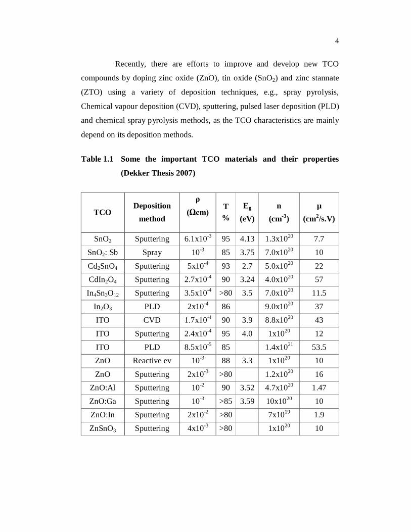
the important TCO materials and their properties are listed in Table 1.1.
4
Recently, there are efforts to improve and develop new TCO
compounds by doping zinc oxide (ZnO), tin oxide (SnO2) and zinc stannate
(ZTO) using a variety of deposition techniques, e.g., spray pyrolysis,
Chemical vapour deposition (CVD), sputtering, pulsed laser deposition (PLD)
and chemical spray pyrolysis methods, as the TCO characteristics are mainly
depend on its deposition methods.
Table 1.1 Some the important TCO materials and their properties
Ion Beam Sputtering, Ion Plating and Filtered Vacuum Arc Deposition. Each
of these techniques has its own advantages and disadvantages. However, the
use of these coatings for commercial applications will be feasible only if they
can be produced in large area at low cost. Even though different methods are
proposed from time to time for the production of TCO in industrial scale,
spray pyrolysis and sputtering are the most widely used techniques due to
their simplicity, reproducible results and capable to coat on large area
substrates. In the following sections some of the important thin film
deposition methods, used for TCO deposition are discussed in detail.
8
1.2.1 Physical Vapour Deposition (PVD)
Physical vapour deposition (PVD) is a process for transferring atoms or molecules from a source to a substrate that relies on physical methods to produce the vapour species. Some of the physical deposition methods are discussed in the following sections.
1.2.1.1 Vacuum Evaporation
Vacuum evaporation (including sublimation) is a physical vapour deposition (PVD) process, where the material is thermally vaporized from a source and deposited on the substrate without collision with the gas molecules present in the space between the source and substrate. Vacuum evaporation experiments are normally conducted in a gas pressure range of 10-5 to 10-9 Torr, which determines the level of contamination in the deposited film (Seshan 2002).
Deposition of thin films by vacuum evaporation is a very simple, convenient, and widely used technique. In this method, evaporation of the material takes place in vacuum environment. Sufficient amount of heat is supplied to the evaporant to attain the desired vapour pressure, and the evaporated material is allowed to condense on the substrate maintained at a required temperature (Hartnagel et al 1995). Vacuum evaporation is possible for a wide range of materials, particularly for metals except the refractory metals with low vapour pressures. By heating the materials, the vapour pressure of the charge is raised to a level at which the evaporation and sublimation occurs. The important process parameters are the substrate material, source and substrate temperatures, source-substrate distance, background gas composition and pressure. Using this method, evaporants with the extraordinary range of chemical reactivity and vapour pressures can be deposited. This method leads to a large diversity in source designs including resistance-heated filaments, electron beams, crucibles heated by conduction, radiation, or rf-induction, arcs, exploding wires, and lasers.
9
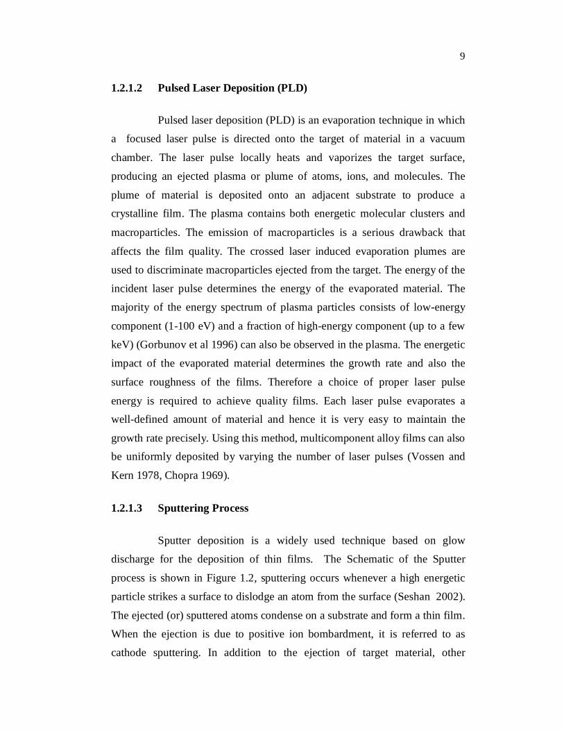
1.2.1.2 Pulsed Laser Deposition (PLD)
Pulsed laser deposition (PLD) is an evaporation technique in which
a focused laser pulse is directed onto the target of material in a vacuum
chamber. The laser pulse locally heats and vaporizes the target surface,
producing an ejected plasma or plume of atoms, ions, and molecules. The
plume of material is deposited onto an adjacent substrate to produce a crystalline film. The plasma contains both energetic molecular clusters and
macroparticles. The emission of macroparticles is a serious drawback that
affects the film quality. The crossed laser induced evaporation plumes are
used to discriminate macroparticles ejected from the target. The energy of the
incident laser pulse determines the energy of the evaporated material. The
majority of the energy spectrum of plasma particles consists of low-energy
component (1-100 eV) and a fraction of high-energy component (up to a few
keV) (Gorbunov et al 1996) can also be observed in the plasma. The energetic
impact of the evaporated material determines the growth rate and also the
surface roughness of the films. Therefore a choice of proper laser pulse
energy is required to achieve quality films. Each laser pulse evaporates a well-defined amount of material and hence it is very easy to maintain the
growth rate precisely. Using this method, multicomponent alloy films can also be uniformly deposited by varying the number of laser pulses (Vossen and
Kern 1978, Chopra 1969).
1.2.1.3 Sputtering Process
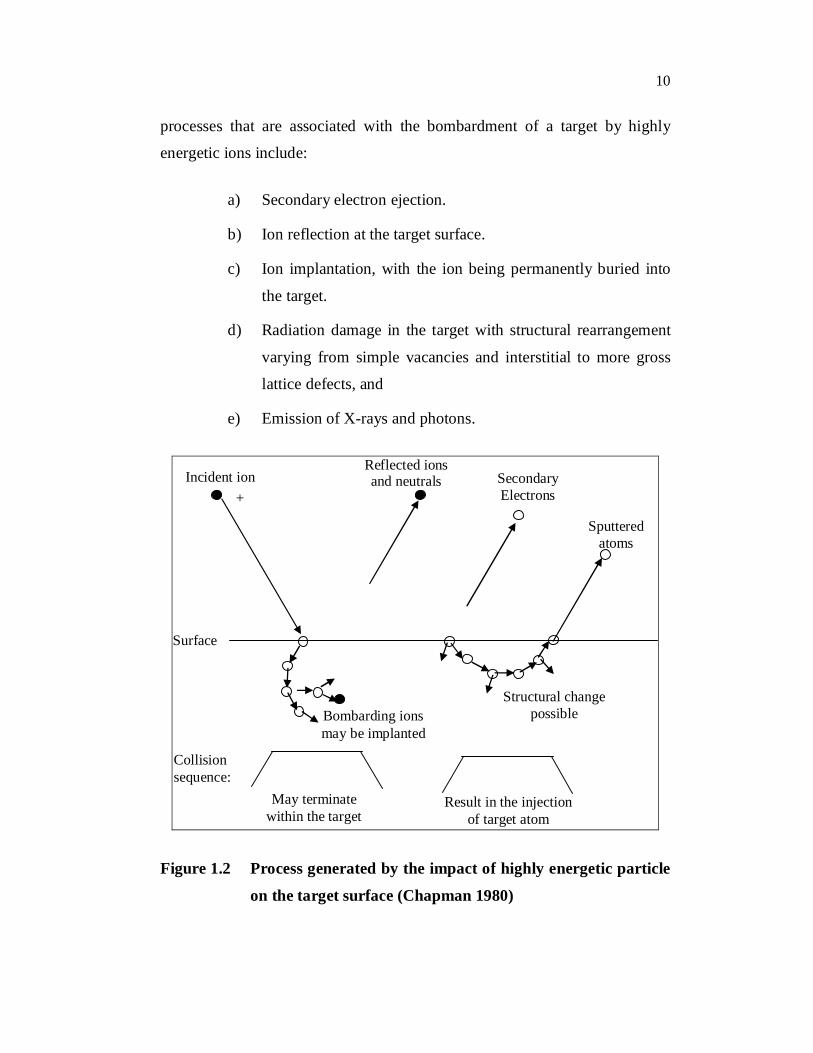
Sputter deposition is a widely used technique based on glow
discharge for the deposition of thin films. The Schematic of the Sputter
process is shown in Figure 1.2, sputtering occurs whenever a high energetic
particle strikes a surface to dislodge an atom from the surface (Seshan 2002).
The ejected (or) sputtered atoms condense on a substrate and form a thin film.
When the ejection is due to positive ion bombardment, it is referred to as
cathode sputtering. In addition to the ejection of target material, other
10
processes that are associated with the bombardment of a target by highly
energetic ions include:
a) Secondary electron ejection.
b) Ion reflection at the target surface.
c) Ion implantation, with the ion being permanently buried into
the target.
d) Radiation damage in the target with structural rearrangement
varying from simple vacancies and interstitial to more gross
lattice defects, and
e) Emission of X-rays and photons.
Incident ion
Reflected ions and neutrals Secondary
Electrons
Sputtered atoms
Bombarding ions may be implanted
Structural change possible
May terminate within the target
Result in the injection of target atom
Collision sequence:
Surface
+
Figure 1.2 Process generated by the impact of highly energetic particle
on the target surface (Chapman 1980)
11
The sputter process is the widely practiced physical vapour deposition method
for industrial applications of large area coatings. Both reactive and non-
reactive forms of DC and RF sputtering and, recently, magnetron and ion
beam have also been used for special purposes.
1.2.1.3.1 Reactive sputtering
Reactive sputtering is the widely used process for producing coatings of compounds. Most metal atoms are sputtered from a metallic target, and sufficient reactive gas, like Ar-O2 or Ar-N2 gas mixture is added to the chamber to form the desired component on the substrate. In addition, when compounds with multiple elements are to be deposited, the composition of the deposited film often differs from the composition of the target due to the fact that the compounds decompose during the sputtering, though the situation varies according to the chemical bond strength between the components. The concentration of the volatile components, such as oxygen and nitrogen, is reduced in the deposited film. Simultaneously, during deposition the target surface composition also changes. To maintain the stoichiometry, reactive gas of the volatile components is added into the plasma. The reactive sputter process in general possess higher growth rate typically in the range of 10 to 30 nm/min when an Ar-O2 mixture is used and is about 5 nm/min for pure O2 atmosphere.
1.2.1.3.2 Sputtering from oxide targets
If the sputter cathode is an oxide or an insulator material, the DC sputtering is not possible due to the building up of positive (Ar+) surface charges. However, a high frequency alternating potential may be used to neutralize the insulator surface periodically with plasma electrons, which have much higher mobility than the positive ions. It is an indispensable technique for deposition of thin films of semiconductor and insulators. The DC and RF diodes are similar in basic configuration, but differ in the power supply
12
frequency. Sputtering at lower pressures (10-3 torr) is possible if the RF configuration is used due to their higher plasma density.
1.2.2 Chemical Vapour Deposition (CVD)
Chemical vapour deposition (CVD) is a surface reaction on a solid surface, where one or more gaseous reacting species are involved. When the vapourized species is incident on a substrate, it produces a film of desired composition. CVD process entirely differs from PVD process, which does not require high vacuum (or) unusual levels of electric power. This technique is versatile for synthesizing both simple and complex compounds. The main control parameters are gas flow, gas composition, substrate temperature and the geometry of deposition apparatus. The deposition rate depends mainly on both the gas flow rate and substrate temperature. The typical growth rates ranges from 30 to 100 nm/min. In CVD process, the geometry of the deposition system is more important for large-scale applications (Blocher 1981, Kalbskopf 1981). Secondly, the chemical reaction is an important part of this technique and requires lot of understanding about the reaction mechanism. Various types of chemical reactions are utilized in CVD (Figure 1.3) for thin film deposition.
Figure 1.3 A schematic drawing of the CVD technique (Hartnagel et al
1995)
13
In one type of reaction, a vapour precursor that contains the
material to be deposited is decomposed by reduction, e.g. using hydrogen at
an elevated temperature. Decomposition is accomplished by thermal
activation. Alternatively, plasma activation may be used to reduce or
decompose the precursor at a lower temperature than the thermal activation.
The different steps involved in a CVD process.
(i) Convective and diffusive transport of reactants from the gas
inlets to the reaction zone.
(ii) Chemical reaction in the gas phase to produce the product and
by products. Transport of the initial reactants and their
products to the substrate surface.
(iii) Adsorption (chemical and physical) and diffusion of these
species on the substrate surface.
(iv) Heterogeneous reactions catalyzed by the surface leading to
film.
(v) Desorption of volatile by-products of the surface leading to
film.
(vi) Convective and diffusive transport of reaction by products
away from the reaction zone.
A variety of modified CVD processes exists namely metalorganic
CVD (MOCVD) when a plasma is used to induce or enhance decomposition
and reaction; low pressure CVD (LPCVD) when the pressure is less than
ambient; and low pressure plasma enhanced CVD (PECVD) when the
pressure is low enough that ions can be accelerated to appreciable energies
from the plasma.
14
1.2.3 Epitaxial Growth of Thin Films
Epitaxy describes the extended single-crystal growth of a film on a
crystalline substrate. Depending on the growth conditions and the substrate
quality, the epitaxial films are extremely perfect in crystalline quality and
defect free. Epitaxial growth methods are generally used for semiconductor
device fabrication, as they can be produced with greater purity than bulk
material.
The two types of epitaxial growth are: (i) homoepitaxy, in which
the film is grown on a crystalline substrate of the same material, and
(ii) heteroepitaxy, in which the film and substrate are different. Homoepitaxy
has the advantage that the substrate and the film have the same lattice
constant, provided the substrate surface is perfectly clean. It can also serve as
a template to facilitate the growth of film as a single crystal. Despite the
mismatch between the film and substrate in the heteroepitaxy, a clean and
oriented substrate provides a template for deposited atoms even though this
may introduce strain in the film. The different types of epitaxy are described
in the following sections.
1.2.3.1 Molecular-beam epitaxy
Molecular-beam epitaxy (MBE) is the simplest as well as well
understood epitaxial process. MBE is a physical deposition process, in which
the deposition occurs by the interaction of beams of atoms / molecules with a
clean substrate surface maintained in ultra high vacuum (UHV). The beams
are generated by the thermal evaporation of the constituent elements
contained in refractory crucibles and is arranged such that the beams can be
conveniently turned on and off. This setup allows the growth of a specific
material to be initiated or terminated extremely rapidly. The UHV
15
environment prevents contamination of the surface, when growth is not taking
place and also allows a variety of in-build analytical tools for characterization
in the same vacuum chamber for in-situ surface analysis, beam-flux
measurements and film-structure studies (Cho 1994).
1.2.3.2 Vapour-phase epitaxy
Vapour-phase epitaxy (VPE) is a chemical deposition process. VPE
has evolved from the CVD of Si on Si substrates. VPE has been used from the
early days for Si device processing to prepare thin layers of silicon with
properties superior to those of the bulk substrate material. The deposition is
typically carried out at pressures ranging from a few Torr to atmospheric
pressure (Houng 1992). This has the advantage of simplifying the apparatus
and increasing the growth rate. However, the complex fluid flow of reactant
gases at these pressures is difficult to model.
1.2.3.3 Liquid-phase epitaxy
Liquid-phase epitaxy (LPE) involves the growth of an epitaxial film
on a substrate that is placed in contact with a saturated solution of the film
material. In some cases, the solvent may be one of the film constituents; e.g.
GaAs films grown from a saturated solution of as in molten Gallium. When
the solution is cooled slightly, it becomes supersaturated and growth occurs
on the substrate (Funitoshi et al 1997)
1.2.3.4 Solid-phase epitaxy
Solid-phase epitaxy (SPE) describes the re-growth of a
polycrystalline amorphous film on a crystalline substrate at an elevated
temperature. The most common example of SPE is the re-growth of a
semiconductor over an amorphized surface of the same semiconductor
16
material. Generally, the amorphization of the semiconductor surface is
achieved by ion implantation. Annealing causes re-growth of the films from
the unimplanted region.
1.2.4 Solution Methods of Deposition
The solution methods of coatings are inexpensive and relatively
easy method, which can be easily scaled up from small scale laboratory
experiments to large area industrial applications. Any hydrolysable
compounds such as halides, nitrate, nitrides and preferably metallo-organic
alkoxide precursors are necessary for this kind of deposition. The three
different types of thin film deposition methods are: spin coating, dip coating
and spray pyrolysis. Details of these methods are given in the following
sections.
1.2.4.1 Spin coating
Spin coating is a simple and widely used technique for depositing
thin films on wafer surfaces. In this method, an excess amount of a solution is
placed on a substrate, which is then rotated at high speed around an axis
perpendicular to the coating area. Due to the centrifugal force, the liquid
evenly spreads on the substrate surface and forms thin films. The process
involves simple fluid flow and evaporation behaviors, which normally allow
the formation of uniform coatings (Birnie and Manley 1997). The spin coating
process can be divided into four stages as shown in Figure 1.4. The
deposition, spin up, and spin off stages occur sequentially, while the
evaporation occurs throughout the process.
17
Figure 1.4 The four stages of the Spin coating process
The deposition process involves the dispense of an excessive amount of fluid onto a stationary or slowly spinning substrate. The fluid is deposited through a nozzle at the center of the substrate or over some programmed path. An excessive amount of fluid is used to prevent coating discontinuities.
In the spin up stage, the substrate is accelerated to the final spin speed. As rotational forces are transferred upward through the fluid, a wave front that forms and flows to the substrate edge by centrifugal force forms a fairly uniform layer. In the spin off stage, the excess solvent is flung off the substrate surface as it rotates at speeds between 2000 and 8000 RPMs. The fluid is being thinned primarily by centrifugal forces until enough solvent has been removed to increase the viscosity to a level, where flow ceases. The spin off stage takes place for approximately 10 seconds after spin up.
In this method, evaporation becomes a crucial parameter that determines the film thinning and quality of the final deposits. Evaporation is the complex process by which a portion of the excess solvent is absorbed into the atmosphere. If significant evaporation occurs prematurely, a solid skin
18
forms on the fluid surface, which impedes the evaporation of solvent trapped under this skin and causes coating defects when subjected to the centrifugal forces of the spinning substrate.
Films of various of film thickness can be deposited by spin coating, due to the fact that film thickness is roughly inversely proportional to the square root of spin speed. As coating thicknesses increases, it becomes difficult to find a solvent / solute mixture, which would not dry before reaching the substrate edge. For this reason, thick films are occasionally formed by spinning on multiple thinner and more reliable coatings.
1.2.4.2 Dip coating
The dip coating method consists of inserting the substrate into a solution containing hydrolysable metal compounds and pulling it out at a constant speed under controlled temperature and atmospheric conditions. In this atmosphere, hydrolysis and condensation processes take place. The coating thickness mainly depends on the withdrawal speed, the solid content and the viscosity of the liquid. In this method, the films are hardened by high temperature treatments. The rate of heating needs to be controlled to avoid cracking of the films (Brinker et al 1991). This method has been commercially used to deposit coatings on both side of a glass substrate on large area coatings (about 10 to 12 m2).
1.2.4.3 Spray pyrolysis
The spray pyrolysis technique involves spraying of a solution (usually aqueous, containing soluble salts of the constituent atoms of the desired compound) onto a substrate maintained at elevated temperatures. The sprayed droplet reacts with the hot substrate surface and undergoes a pyrolytic (endothermic) decomposition and forms single crystallite or cluster of crystallites of the compounds. The other volatile by-products and the excess solvent escape in the vapour phase. The substrate provides the thermal energy
19
for the thermal decomposition and the subsequent recombination of the constituent species followed by sintering and recrystallisation of the clusters of crystallites to form a coherent film (Shanthi 1999).
Spray pyrolysis has been used to deposit thin films and prepare compound powder material. Even multilayered films can easily be prepared using this versatile technique. Unlike many other film deposition techniques, spray pyrolysis represents a very simple and relatively cost-effective processing method. It is an extremely easy method for preparing films of any composition. The working principles of spray technique are: (i) the solution either from a reservoir or in vapour phase is carried using some carrier gas like argon, nitrogen or compressed air and (ii) the solution or the vapour is then sprayed by the atomizer onto the hot substrate. The quality of these films depends on parameters such as the spray rate, the substrate temperature and the ratio of various constituents in the solutions. Thin-film deposition using spray pyrolysis can be divided into three main steps: (i) atomization of the precursor solution, (ii) transportation of the resultant aerosol, and (iii) decomposition of the precursor on the substrate (Perednis and Gauckler 2005).
In spray pyrolysis, the important factor is to understand the basic atomization process of the atomization device used. Depending on the application of the films, one can choose the atomizers like air blast, ultrasonic, and electrostatic atomizers, etc.
During aerosol transport, it is important that as many droplets as possible are transported to the substrate without forming powder or salt particles. Sears and Michael (1988) investigated the mechanism of SnO2 film growth. They studied the influence of forces, which determine both the trajectory of the droplets and evaporation and proposed a film growth model considering the gravitational, electric, thermophoretic and Stokes forces. Sears and Michael (1988), Yu and Liao (1998) developed a model to describe
20
the evaporation of solution droplets before forming a solid crust by considering the mass transfer, momentum, temperature outside and around the droplet as well as effects of precursor precipitation. The main drawback of this model is the interactions between droplets were ignored. Yu and Liao (1998), Lenggoro et al (2000) investigated the powder production by spray pyrolysis using a temperature-graded laminar flow aerosol reactor and calculated the evaporation rate and the change of the precursor concentration within the droplets, which showed good agreement between the simulated as well as experimental results (Lenggoro et al 2000).
During decomposition of the precursor, various processes occur simultaneously (evaporation of residual solvent, spreading of the droplet, and salt decomposition), when a droplet hits the surface of the substrate. Several models have been developed to explain the decomposition mechanism of a precursor. The chemical vapour deposition based process that gives high quality films by spray pyrolysis is claimed as one of the best suited techniques. Figure 1.5 shows the decomposition of the precursor when increasing the substrate temperature (Perednis and Gauckler 2005).
Figure 1.5 Description of the deposition processes initiated with
increasing substrate temperature
21
In general, among the solution based deposition techniques, spray
pyrolysis is a versatile and effective technique to deposit metal oxide films,
which could be scaled up from small scale laboratory experiments to large
scale industrial applications with less investments. The most important
parameter is the substrate temperature and if the substrate temperature is
higher, then the films possess more roughness as well as porous. When the
temperature is too low, cracks would be observed in the films. The substrate
temperature also influences the crystallinity, texture, and other physical
properties of the deposited films. Another important spray parameter is the
viscosity of the precursor solution that affects the morphology and properties
of the deposited films. The film morphology and properties can also be
changed by using various additives in the precursor solution (Perednis and
Gauckler 2005) with such advantages of this spray pyrolysis technique, we
have selected this method for the preparation of thin film samples. More
details on the experimental setup and the steps involved in the process
optimization are discussed in Chapter 2.
1.3 SCOPE OF THE PRESENT WORK
From the materials science point of view to be able to engineer and
optimize transparent conducting oxide (TCO) coatings for modern
applications, it is essential to study the material characteristics, in particular
the structural, optical and electrical properties, which are essential for the
further developments of TCO coatings. In this investigation, we have studied
the preparation conditions and properties of Al and Cd doped ZnO, Zn doped
SnO2 and Zn2SnO4 films. These films were prepared by chemical spray
pyrolysis method with a substrate temperature of 400oC. The effect of the
different process parameters on the structure, lattice parameters, thickness,
surface roughness, optical and sheet resistance properties has been
investigated. In addition, the effect of post growth annealing on the above said
properties has also been investigated for Zn2SnO4 films. Energy dispersive
22
X-ray diffraction (EDX) was employed to determine the chemical
composition of the films. The structure of the films has been studied by X-ray
diffraction (XRD) method. For the precise determination of optical constants,
optical spectroscopy and ellipsometric techniques have been used. The sheet
resistance of the films has been measured by four probe method in the van der
Pauw configuration. A combination of the results obtained from these
measurements is expected to provide an in-depth knowledge on the film
properties. This information is important for the understanding of the
chemical spray pyrolysis process and for the further development of the
performance of the TCOs.
The objectives of the present research are:
Deposition of Al and Cd doped ZnO, Zn doped SnO2 and Zn2SnO4 thin films by chemical spray pyrolysis method.
Optimization of deposition conditions for films with high optical transmission, lowest electrical resistivity with good reproducibility.
Comparison of characteristics of Zn2SnO4 thin films with Al and Cd doped ZnO and Zn doped SnO2 thin films deposited by chemical spray pyrolysis technique.
It was expected that by optimizing the deposition parameters of Al and Cd doped ZnO, Zn doped SnO2, and Zn2SnO4 thin films, some improvement in the film properties might be achieved. The research for an improved TCO involves the study of structural, electrical and optical properties as a function of the deposition parameters and doping element concentration in the films. These films have the potential to overcome current TCO problems and also would help the scientific community to identify non indium based TCO coatings for modern applications.