21
Chapter 16 Frequency Effects
| Date post: | 03-Jan-2016 |
| Category: |
Documents |
| Upload: | illiana-bentley |
| View: | 16 times |
| Download: | 0 times |

Chapter 16
Frequency Effects

0.707 Amid
A
f
Amid
The frequency response curve of an ac amplifier
f1 f210f1 0.1f2
The cutoff frequenciesAlso called the half-power frequencies
The midband
The gain is maximum in the midband.
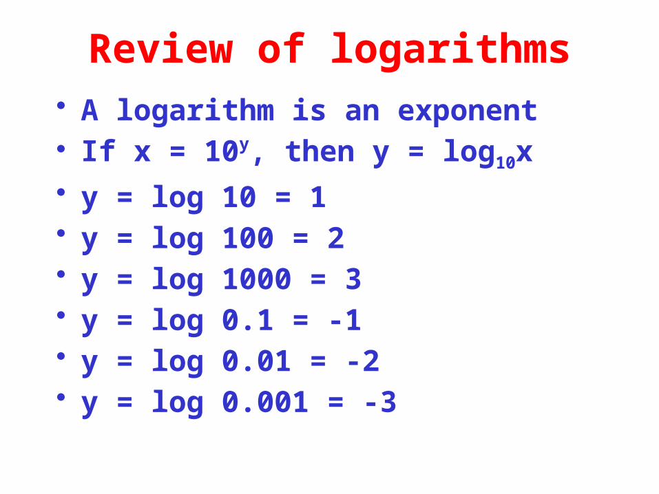
Review of logarithms• A logarithm is an exponent• If x = 10y, then y = log10x
• y = log 10 = 1• y = log 100 = 2• y = log 1000 = 3• y = log 0.1 = -1• y = log 0.01 = -2• y = log 0.001 = -3

Definition of GdB
• G = pout/pin
• GdB = 10 log G
• Memorize:– if G = 2, GdB = +3
– if G = 0.5, GdB = -3
– if G = 10, GdB = +10
– if G = 0.1, GdB = -10

Definition of AdB
• A = vout/vin
• Adb = 20 log A
• Memorize:> if A = 2, AdB = +6
> if A = 0.5, AdB = -6
> if A = 10, AdB = +20
> if A = 0.1, AdB = -20
• Cascade: A = A1A2, AdB = A1dB + A2dB

More on the decibel
• GdB = AdB only if impedance matched
• G = antilog GdB/10
• A = antilog AdB/20
• PdBm = 10 log P/1 mW
• P = antilog PdBm/10
• VdBV = 20 log V
• V = antilog VdBV/20
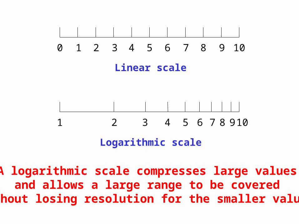
1 2 3 4 5 6 7 8 9 10
1 2 3 4 5 6 7 8 9 100
Logarithmic scale
Linear scale
A logarithmic scale compresses large values and allows a large range to be covered
without losing resolution for the smaller values.

Bode plots
• Use semilogarithmic graph paper (the horizontal axis is logarithmic; the vertical is linear)
• Plot dB voltage gain on the vertical axis• Plot frequency on the horizontal axis• An octave refers to a ratio of 2• A decade refers to a ratio of 10

10 Hz 100 Hz 1 kHz 10 kHz 100 kHz 1 MHz 10 MHz
50 dB
40 dB
30 dB
20 dB
10 dB
0 dB
Ideal Bode plot of an ac amplifier
Midbandgain
Cutoff (-3dB) frequencies*
20 dB/decaderolloff
*also called corner or break frequencies
Unity gainfrequency
Unity gainfrequency

R
C
Amplitude responseof RC lag circuit
0 dB
-20 dB
-40 dB
-60 dB
10f2f2 100f2 1000f2
f2 = 2pRC1
f2
f( )2
1+
1A =

0o
0.1f2 f2 10f2
Angular responseof RC lag circuit
-90o
-45o
R
C
f2
ff = -arctan

10 Hz 100 Hz 1 kHz 10 kHz 100 kHz
50 dB
40 dB
30 dB
20 dB
10 dB
0 dB
Ideal Bode plot of a dc amplifier with two break frequencies.
20 dB/decade
40 dB/decade
fb1 fb2

Invertingamplifier
Avin vout
Invertingamplifier
Avin vout
C
Cin Cout
Miller equivalent circuit
Inverting amplifier with feedback capacitor
Cin = C(A+1) Cout = C A+1A

Frequency compensation• Most op amps are internally
compensated to prevent oscillations• One dominant internal compensation
capacitor rolls off the gain at 20 dB/decade
• IC capacitors are limited to the pF range• The Miller effect makes the internal
compensation capacitor equivalent to a much larger capacitor

R
C
Square-wave response of a circuit with limited bandwidth
0
V0.9V
0.1V
TR
TR = 2.2RC
fcutoff = 0.35
TR
0
V

+VCC
RER2
RC
R1
RL
vG
Cutoff frequency of input coupling capacitor
RG
zin(stage) = R1 R2 bre’
C
f1 = 2p(RG + zin(stage))C
1f1
A
f
+VCC
RER2
RC
R1
RL
vG
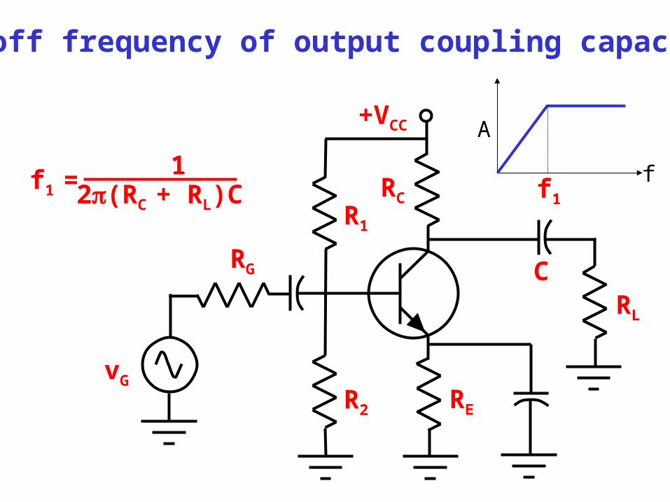
Cutoff frequency of output coupling capacitor
RG C
f1
A
ff1 = 2p(RC + RL)C
1

+VCC
RER2
RC
R1
RL
vG
Cutoff frequency of emitter bypass capacitor
RG
C
f1
A
ff1 =
2 p zoutC1
re’ +
R1 R2 RG
b( )zout = RE

Combined frequency effects• The input coupling, output coupling, and
emitter bypass capacitors each produce a cutoff frequency.
• One is usually dominant (the highest frequency) and produces a rolloff of 20 dB/decade as frequency decreases.
• When the next cutoff is reached, the gain rolloff increases to 40 dB/decade.
• When the third is reached, it becomes 60 dB/decade.

Base and collector bypass circuits
C’e
f2
A
f
CMiller Cstray
CMiller
C’e
C’c
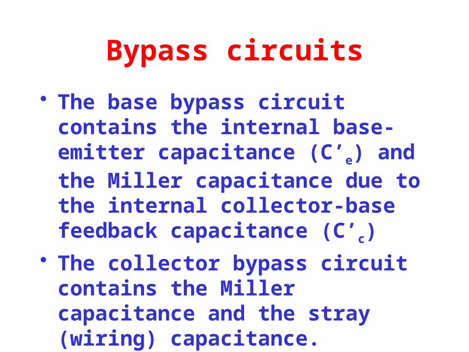
Bypass circuits
• The base bypass circuit contains the internal base-emitter capacitance (C’e) and the Miller capacitance due to the internal collector-base feedback capacitance (C’c)
• The collector bypass circuit contains the Miller capacitance and the stray (wiring) capacitance.


