2019 Edition Chapter 17: Test Technology Section 07: Wafer Probe and Device Handling http://eps.ieee.org/hir We acknowledge with gratitude the use of material and figures in this Roadmap that are excerpted from original sources. Figures & tables should be re-used only with the permission of the original source. The HIR is devised and intended for technology assessment only and is without regard to any commercial considerations pertaining to individual products or equipment.
Transcript
2019 Edition
Chapter 17: Test Technology
Section 07: Wafer Probe and Device Handling
http://eps.ieee.org/hir
We acknowledge with gratitude the use of material and figures in this Roadmap that are excerpted from original sources. Figures & tables should be re-used only with the permission of the original source.
The HIR is devised and intended for technology assessment only and is without regard to any commercial considerations pertaining to individual products or equipment.
HIR version 1.0 (eps.ieee.org/hir) Chapter 17, Page 35 Heterogeneous Integration Roadmap
Section 7: Wafer Probe and Device Handling
Wafer probe and component test handling equipment face significant technical challenges in each market segment. Common issues on both platforms include higher parallelism and increasing capital equipment and interface cost.
Device Handling Trends
Increased parallelism at wafer probe drives a greater span of probes across the wafer surface and significantly increased probe card complexity. Prober and probe card architecture should evolve to simplify the interface, however just the opposite is happening: ATE tester complexity is decreasing and more technology and complexity is built into the probe card interface. A better thermal solution is a very important parameter along with performance for better yield management. Memory applications are increasing the total power across a 300mm wafer, and wafer probe needs to dissipate this total power to sustain the set-temperature during test. Power density per DUT is increasing and it’s very challenging to manage a stable wafer-level test temperature. 3D integration technology requires very precise probing technology in X, Y and Z, as micro-bumps may be easily damaged during the probing process. MEMS applications require a variety of testing environments such as pressure, magnetic, and vacuum environments; also, wafer shape and package style are becoming very unique depending on the application type.
Reducing the cost of wafer-level and package-level test in the face of more challenging technology and performance requirements is a constant goal. The demand for higher throughput must be met by either increased parallelism (even with reduced test times), faster handler speed, or process improvements such as asynchronous test or continuous-lot processing. 3D integration technology requires new contact technology for the intermediate test insertion which will be added between conventional front-end process and back-end process. New contact technology to probe on the singulated and possibly thinned die’s micro-bumps or C4 bumps after the die is mounted on an interposer is needed. For the die-level handler, the main tasks are the alignment accuracy to enable fine pitch contact, die level handling without damaging the die, and the tray design that supplies/receives the die.
Packages continue to shrink, substrates are getting thinner, and the package areas available for handling are getting smaller at the same time that the lead/ball/pad count is increasing. In the future, die-level handlers as well as package handlers will need the capability to very accurately pick and place small, fragile parts, yet apply similar or increasing insertion force without inducing damage.
Temperature ranges are expanding to meet more stringent end-use conditions, and there is a need for better control of the junction temperature, immediate heat control technology, and temperature control to enable stable DUT temperature at the start of test. Power dissipation overall appears to be increasing, but multi-core technology is offering relief in some areas.
It is unlikely that there will be one handler that is all things to all users. Integration of all of the technology to meet wide temperature range, high temperature accuracy, high throughput, placement accuracy, parallelism, and special handling needs while still being cost effective in a competitive environment is a significant challenge.
Gravity feed, turret, and strip handlers have been added to the table while retaining the pick and place type handler. The gravity feed handler is used on SOP, QFN, and DIP packages. Turret handlers are widely used on discrete-type QFN devices. Strip handlers are used on the frame before singulation. Strip test enables high parallelism with fewer interface resources, which enables cheaper test cost. These additional three types of handlers are widely used on relatively low-end or low-cost devices. Evolution of these handlers is quite different but important for various type of LSI.
June, 2019 Test Technology
HIR version 1.0 (eps.ieee.org/hir) Chapter 17, Page 36 Heterogeneous Integration Roadmap
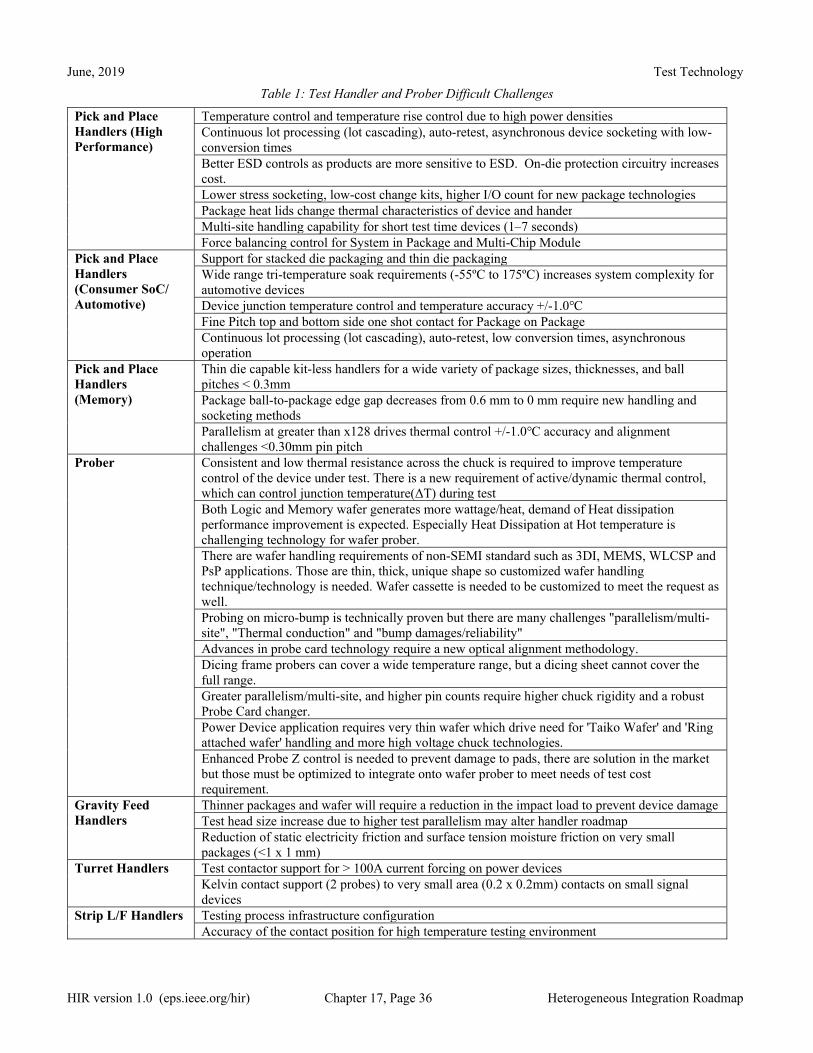
Table 1: Test Handler and Prober Difficult Challenges
Pick and Place Handlers (High Performance)
Temperature control and temperature rise control due to high power densities Continuous lot processing (lot cascading), auto-retest, asynchronous device socketing with low-conversion times Better ESD controls as products are more sensitive to ESD. On-die protection circuitry increases cost. Lower stress socketing, low-cost change kits, higher I/O count for new package technologies Package heat lids change thermal characteristics of device and hander Multi-site handling capability for short test time devices (1–7 seconds) Force balancing control for System in Package and Multi-Chip Module
Pick and Place Handlers (Consumer SoC/ Automotive)
Support for stacked die packaging and thin die packagingWide range tri-temperature soak requirements (-55ºC to 175ºC) increases system complexity for automotive devices Device junction temperature control and temperature accuracy +/-1.0℃ Fine Pitch top and bottom side one shot contact for Package on Package Continuous lot processing (lot cascading), auto-retest, low conversion times, asynchronous operation
Pick and Place Handlers (Memory)
Thin die capable kit-less handlers for a wide variety of package sizes, thicknesses, and ball pitches < 0.3mm Package ball-to-package edge gap decreases from 0.6 mm to 0 mm require new handling and socketing methods Parallelism at greater than x128 drives thermal control +/-1.0℃ accuracy and alignment challenges <0.30mm pin pitch
Prober Consistent and low thermal resistance across the chuck is required to improve temperature control of the device under test. There is a new requirement of active/dynamic thermal control, which can control junction temperature(ΔT) during testBoth Logic and Memory wafer generates more wattage/heat, demand of Heat dissipation performance improvement is expected. Especially Heat Dissipation at Hot temperature is challenging technology for wafer prober.There are wafer handling requirements of non-SEMI standard such as 3DI, MEMS, WLCSP and PsP applications. Those are thin, thick, unique shape so customized wafer handling technique/technology is needed. Wafer cassette is needed to be customized to meet the request as well. Probing on micro-bump is technically proven but there are many challenges "parallelism/multi-site", "Thermal conduction" and "bump damages/reliability"Advances in probe card technology require a new optical alignment methodology. Dicing frame probers can cover a wide temperature range, but a dicing sheet cannot cover the full range. Greater parallelism/multi-site, and higher pin counts require higher chuck rigidity and a robust Probe Card changer. Power Device application requires very thin wafer which drive need for 'Taiko Wafer' and 'Ring attached wafer' handling and more high voltage chuck technologies.Enhanced Probe Z control is needed to prevent damage to pads, there are solution in the market but those must be optimized to integrate onto wafer prober to meet needs of test cost requirement.
Gravity Feed Handlers
Thinner packages and wafer will require a reduction in the impact load to prevent device damageTest head size increase due to higher test parallelism may alter handler roadmap Reduction of static electricity friction and surface tension moisture friction on very small packages (<1 x 1 mm)
Turret Handlers Test contactor support for > 100A current forcing on power devicesKelvin contact support (2 probes) to very small area (0.2 x 0.2mm) contacts on small signal devices
Strip L/F Handlers Testing process infrastructure configurationAccuracy of the contact position for high temperature testing environment
June, 2019 Test Technology
HIR version 1.0 (eps.ieee.org/hir) Chapter 17, Page 37 Heterogeneous Integration Roadmap
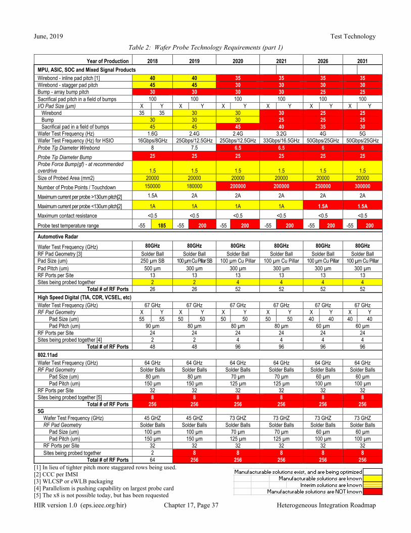
Wirebond - inline pad pitch [1] 40 40 35 35 35 35 Wirebond - stagger pad pitch 45 45 30 30 30 30 Bump - array bump pitch 30 30 30 30 25 25 Sacrifical pad pitch in a field of bumps 100 100 100 100 100 100 I/O Pad Size (µm) X Y X Y X Y X Y X Y X Y Wirebond 35 35 30 30 30 25 25 Bump 30 30 30 25 25 25 Sacrifical pad in a field of bumps 45 45 45 40 35 30 Wafer Test Frequency (Hz) 1.6G 2.4G 2.4G 3.2G 4G 5G Wafer Test Frequency (Hz) for HSIO 16Gbps/8GHz 25Gbps/12.5GHz 25Gbps/12.5GHz 33Gbps/16.5GHz 50Gbps/25GHz 50Gbps/25GHz Probe Tip Diameter Wirebond 8 7.5 6.5 6.5 6 6
Probe Tip Diameter Bump 25 25 25 25 25 25 Probe Force Bump(gf) - at recommended overdrive 1.5 1.5 1.5 1.5 1.5 1.5 Size of Probed Area (mm2) 20000 20000 20000 20000 20000 20000
Number of Probe Points / Touchdown 150000 180000 200000 200000 250000 300000
Maximum current per probe >130um pitch[2] 1.5A 2A 2A 2A 2A 2A
Maximum current per probe <130um pitch[2] 1A 1A 1A 1A 1.5A 1.5A
Maximum contact resistance <0.5 <0.5 <0.5 <0.5 <0.5 <0.5
Probe test temperature range -55 185 -55 200 -55 200 -55 200 -55 200 -55 200
Automotive Radar
Wafer Test Frequency (GHz) 80GHz 80GHz 80GHz 80GHz 80GHz 80GHz RF Pad Geometry [3] Solder Ball Solder Ball Solder Ball Solder Ball Solder Ball Solder Ball Pad Size (um) 250 µm SB 100 µm Cu Pillar SB 100 µm Cu Pillar 100 µm Cu Pillar 100 µm Cu Pillar 100 µm Cu Pillar Pad Pitch (um) 500 µm 300 µm 300 µm 300 µm 300 µm 300 µm RF Ports per Site 13 13 13 13 13 13 Sites being probed together 2 2 4 4 4 4
Total # of RF Ports 26 26 52 52 52 52
High Speed Digital (TIA, CDR, VCSEL, etc) Wafer Test Frequency (GHz) 67 GHz 67 GHz 67 GHz 67 GHz 67 GHz 67 GHz RF Pad Geometry X Y X Y X Y X Y X Y X Y
RF Ports per Site 32 32 32 32 32 32 Sites being probed together 2 8 8 8 8 8
Total # of RF Ports 64 256 256 256 256 256 [1] In lieu of tighter pitch more staggared rows being used. [2] CCC per IMSI [3] WLCSP or eWLB packaging [4] Parallelism is pushing capability on largest probe card [5] The x8 is not possible today, but has been requested
June, 2019 Test Technology
HIR version 1.0 (eps.ieee.org/hir) Chapter 17, Page 38 Heterogeneous Integration Roadmap
HIR version 1.0 (eps.ieee.org/hir) Chapter 17, Page 40 Heterogeneous Integration Roadmap
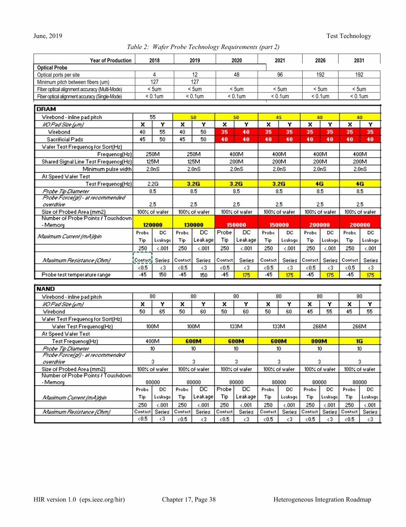
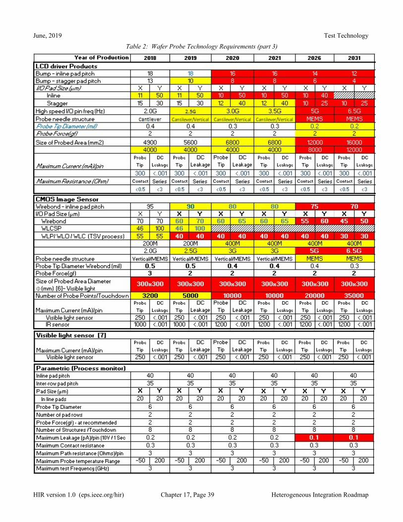
Notes: [6] Probe area is limited by optical system [7] The trend of NIR image sensor circuit design will be similar to visible image sensor. So, the wafer probe table
doesn't need to seperate addional items for NIR image sensor
Test Sockets
The test socket is an electrical and mechanical interface responsible for good electrical connection and transference of high-integrity signals between the DUT and the PCB/tester through a mechanical contact mechanism in order to determine the electrical characteristics of the DUT. As semiconductor design and manufacturing capabilities have progressed in recent years, the testing process keeps raising the electrical and mechanical requirements of test sockets. Therefore, the socket technologies have been rapidly driven by significantly enhanced electrical and mechanical requirements, both of which are instigated by higher power/voltage/current, reduced package size, tighter pitches, higher pin counts, smaller solder resist opening, and so on. It has been indicated that electrical properties are determined by not only the electrical but also by the mechanical requirements. The multi-physics problems have made socket designs progressively challenging for these higher requirements. Current models show difficulty in making sockets for high ball count devices and achieving I/O bandwidths of > 20GHz.
Socket Trends
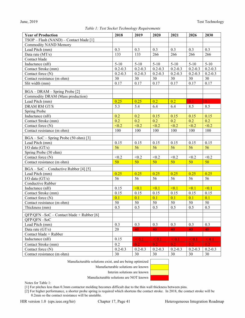
Table 1 contains the test socket technology requirements. The requirements have been divided into contacting NAND, DRAM, and SoC devices that are contained in TSOP, BGA, and BGA SoC packages respectively. The TSOP package is assumed to be contacted using a blade; the DRAM BGA is contacted with a spring probe, and the SoC BGA is contacted with a 50-Ohm spring probe. The test socket performance capability is driven by the pitch between balls or leads, so the lead spacing of the assembly and packaging roadmap was used to determine the pitch.
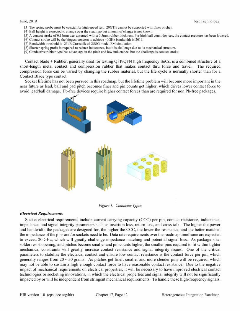
Contact blades are generally used for testing TSOP NAND Flash and contain a spring function in their structure, which is loaded by compressing the DUT into the socket. The structure is very simple and suitable for HVM; however, the contactor blade must be long to maintain the specified contact force and stroke, and to achieve a long mechanical lifetime. A weak point is that the blade contactor is not suitable for fine pitch devices due to the need to have isolation walls between adjacent pins. The thickness of the isolation wall must be thinner for finer pitches, which makes fabrication of the isolation wall more difficult. At the same time, the contactor blade thickness needs to be thinner for finer pitch, which complicates achieving the specified contact force, stroke requirement, and mechanical lifetime.
Spring probes, mainly used for testing BGA-DRAM devices, are formed by use of small-diameter cylindrical parts (probe and socket) and coil springs. Compression of the spring probe creates the contact load. In order to guarantee sufficient mechanical life, the probe diameter should be large enough to guarantee strength and durability and the length should be long enough to maintain sufficient travel under compression. The spring probe structure is relatively simple and easy to maintain and it is also easy to design a DUT loadboard.
According to the BGA-DRAM roadmap, the spring probe diameter will need to be smaller over time, driven by the finer pitch of the package ball roadmap. In addition, the spring probe will need to be shorter to meet the lower inductance values required to support the high frequencies of the roadmap I/O data rate.
Spring 50-Ohm probes required for BGA-SoC high frequency devices have coaxial structures that can reduce probe length transmission issues through impedance matching. However, advances in the package ball pitch through the roadmap will create restrictions to the coaxial pin arrangement structure (0.5 mm pitch in year 2016). The data rate will increase to 20GT/s in 2016, but the spring 50-Ohm probe will not have good electrical performance due to its multiple parts structure having higher contact resistance than other contactors. To support 50milli-Ohms of contact resistance starting in 2016, advances will be required in materials, plating, and structure.
Conductive rubber type contactors are used for BGA high frequency SoC devices. Conductive metal particles are aligned vertically in insulating silicone rubber which enables vertical contact and adjacent conductor isolation. Compared to other contacts, it is superior for uses with high frequency device test due to its low inductance and low contact height, but compression travel is limited. Conductive rubber will meet the fine-pitch requirement in the roadmap, but it is difficult to reduce contact force without decreasing the compression travel.
June, 2019 Test Technology
HIR version 1.0 (eps.ieee.org/hir) Chapter 17, Page 41 Heterogeneous Integration Roadmap
Manufacturable solutions exist, and are being optimized Manufacturable solutions are known
Interim solutions are known Manufacturable solutions are NOT known
Notes for Table 1: [1] For pitches less than 0.3mm contactor molding becomes difficult due to the thin wall thickness between pins. [2] For higher performance, a shorter probe spring is required which shortens the contact stroke. In 2018, the contact stroke will be
0.2mm so the contact resistance will be unstable.
June, 2019 Test Technology
HIR version 1.0 (eps.ieee.org/hir) Chapter 17, Page 42 Heterogeneous Integration Roadmap
[3] The spring probe must be coaxial for high-speed test. 20GT/s cannot be supported with finer pitches. [4] Ball height is expected to change over the roadmap but amount of change is not known.[5] A contact stroke of 0.15mm was assumed with a 0.5mm rubber thickness. For high ball count devices, the contact pressure has been lowered.[6] Contact stroke will be the biggest concern to achieve 40GHz bandwidth in 2019. [7] Bandwidth threshold is -25dB Crosstalk of GSSG model EM simulation.[8] Shorter spring probe is required to reduce inductance, but it is challenge due to its mechanical structure. [9] Conductive rubber type has advantage in the pitch and low inductance, but the challenge is contact stroke. Contact blade + Rubber, generally used for testing QFP/QFN high frequency SoCs, is a combined structure of a
short-length metal contact and compression rubber that makes contact thru force and travel. The required compression force can be varied by changing the rubber material, but the life cycle is normally shorter than for a Contact Blade type contact.
Socket lifetime has not been pursued in this roadmap, but the lifetime problem will become more important in the near future as lead, ball and pad pitch becomes finer and pin counts get higher, which drives lower contact force to avoid lead/ball damage. Pb-free devices require higher contact forces than are required for non Pb-free packages.
Figure 1: Contactor Types
Electrical Requirements
Socket electrical requirements include current carrying capacity (CCC) per pin, contact resistance, inductance, impedance, and signal integrity parameters such as insertion loss, return loss, and cross-talk. The higher the power and bandwidth the packages are designed for, the higher the CCC, the lower the resistance, and the better matched the impedance of the pins and/or sockets need to be. Data rate requirements over the roadmap timeframe are expected to exceed 20 GHz, which will greatly challenge impedance matching and potential signal loss. As package size, solder resist opening, and pitches become smaller and pin counts higher, the smaller pins required to fit within tighter mechanical constraints will greatly increase contact resistance and signal integrity issues. One of the critical parameters to stabilize the electrical contact and ensure low contact resistance is the contact force per pin, which generally ranges from 20 ~ 30 grams. As pitches get finer, smaller and more slender pins will be required, which may not be able to sustain a high enough contact force to have reasonable contact resistance. Due to the negative impact of mechanical requirements on electrical properties, it will be necessary to have improved electrical contact technologies or socketing innovations, in which the electrical properties and signal integrity will not be significantly impacted by or will be independent from stringent mechanical requirements. To handle these high-frequency signals,
June, 2019 Test Technology
HIR version 1.0 (eps.ieee.org/hir) Chapter 17, Page 43 Heterogeneous Integration Roadmap
the user has to carefully consider the signal integrity of the overall test system including board design/components/socket.
Mechanical Requirements
The mechanical requirements include mechanical alignment, compliance, and pin reliability. Mechanical alignment has been greatly challenged by higher pin counts and smaller solder resist openings, particularly in land grid array (LGA) applications. Currently, the majority of test sockets use passive alignment control in which the contact accuracy between pin and solder resist opening is determined by the tolerance stack-up of mechanical guiding mechanisms. The limit of passive alignment capability is quickly being reached because manufacturing tolerance control is approximately a few microns. The employment of active alignment or an optical handling system is one of the options to enable continuous size reduction of package and solder resist opening, smaller pitches, and higher pin counts.
Compliance is considered as the mechanical contact accuracy in the third dimension (Z-direction), in which the total contact stroke should take into account both the co-planarity of operating pin height and the non-flatness of the DUT pins, in addition to a minimum required pin compression. In general, the total stroke of the contact is between 0.3 mm and 0.5 mm. However, as required pin sizes get smaller, it may not be feasible to maintain the same stroke and thus the compression issue may become the bottleneck of electrical contact performance.
Contactor pin reliability and pin tip wear-out have also experienced challenges because tight geometric constraints prevent adding redundant strength to the pins. The testing environment becomes more difficult with higher temperatures, higher currents, smaller pin tip contacts, etc.