27
Chapter 2: Diode Applications © Modified by Yuttapong Jiraraksopakun ENE, KMUTT 2009
Chapter 2: Diode Applications
© Modified by Yuttapong Jiraraksopakun ENE, KMUTT 2009
Copyright ©2009 by Pearson Education, Inc. Upper Saddle River, New Jersey 07458 • All rights reserved.
Electronic Devices and Circuit Theory, 10/e Robert L. Boylestad and Louis Nashelsky
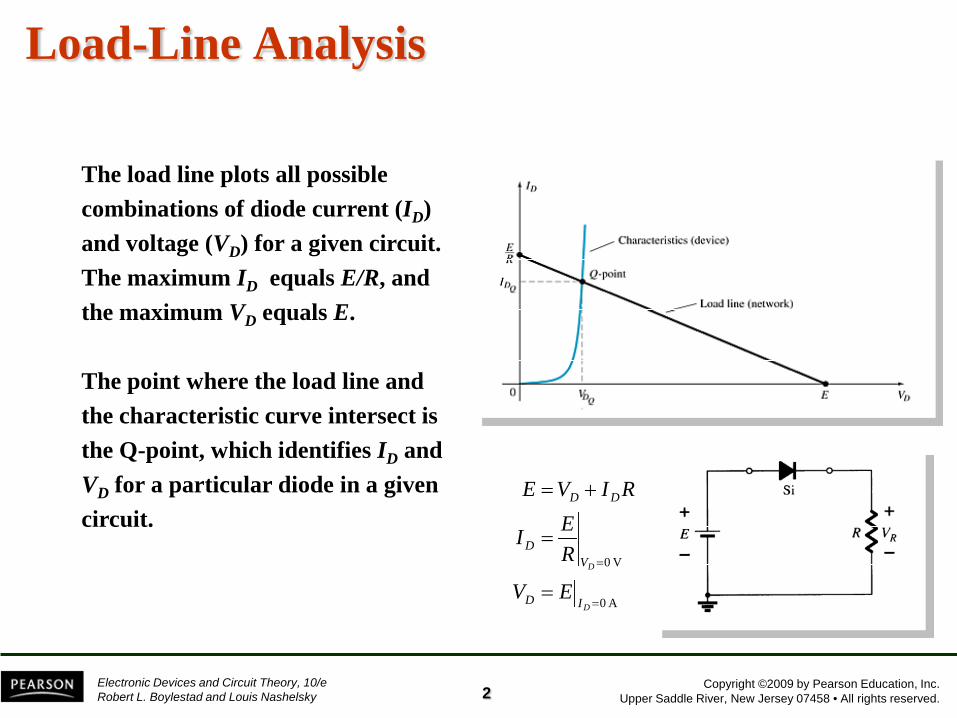
Load-Line Analysis
2
The load line plots all possible combinations of diode current (ID) and voltage (VD) for a given circuit. The maximum ID equals E/R, and the maximum VD equals E. The point where the load line and the characteristic curve intersect is the Q-point, which identifies ID and VD for a particular diode in a given circuit.
A 0
V 0
=
=
=
=
+=
D
D
ID
VD
DD
EV
REI
RIVE

Copyright ©2009 by Pearson Education, Inc. Upper Saddle River, New Jersey 07458 • All rights reserved.
Electronic Devices and Circuit Theory, 10/e Robert L. Boylestad and Louis Nashelsky
Series Diode Configurations
Constants • Silicon Diode: VD = 0.7 V • Germanium Diode: VD = 0.3 V Analysis (for silicon) • VD = 0.7 V (or VD = E if E < 0.7 V) • VR = E – VD
• ID = IR = IT = VR / R
3
Forward Bias
Diodes ideally behave as open circuits Analysis • VD = E • VR = 0 V
• ID = 0 A
Reverse Bias

Copyright ©2009 by Pearson Education, Inc. Upper Saddle River, New Jersey 07458 • All rights reserved.
Electronic Devices and Circuit Theory, 10/e Robert L. Boylestad and Louis Nashelsky
Load-Line Analysis – Examples
4
Find VDQ , IDQ VR
Copyright ©2009 by Pearson Education, Inc. Upper Saddle River, New Jersey 07458 • All rights reserved.
Electronic Devices and Circuit Theory, 10/e Robert L. Boylestad and Louis Nashelsky
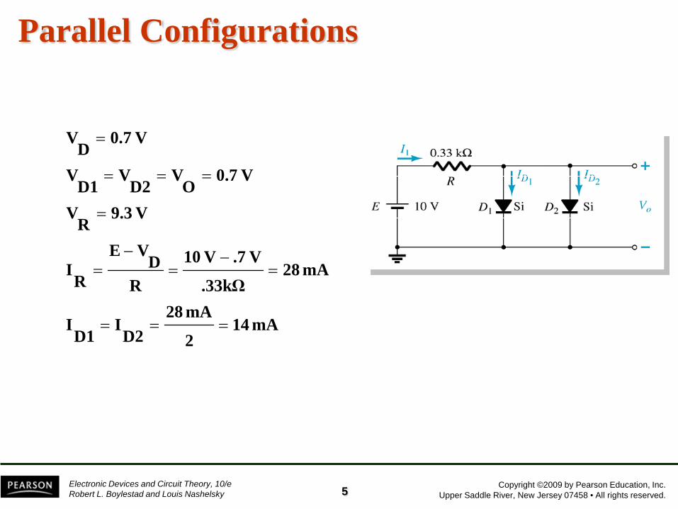
Parallel Configurations
5
mA 142
mA 28D2
ID1
I
mA 28.33kΩ
V .7V 10
RD
VE
RI
V 9.3R
V
V 0.7O
VD2
VD1
V
V 0.7D
V
===
=−
=−
=
=
===
=
Copyright ©2009 by Pearson Education, Inc. Upper Saddle River, New Jersey 07458 • All rights reserved.
Electronic Devices and Circuit Theory, 10/e Robert L. Boylestad and Louis Nashelsky
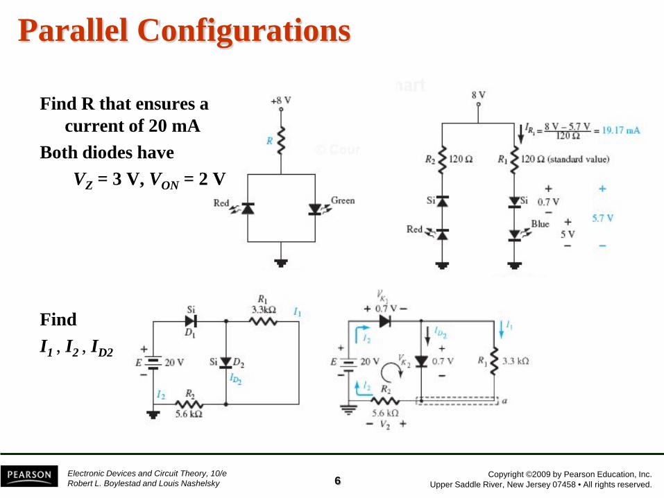
Parallel Configurations
6
Find I1 , I2 , ID2
Find R that ensures a current of 20 mA
Both diodes have VZ = 3 V, VON = 2 V
Copyright ©2009 by Pearson Education, Inc. Upper Saddle River, New Jersey 07458 • All rights reserved.
Electronic Devices and Circuit Theory, 10/e Robert L. Boylestad and Louis Nashelsky
Half-Wave Rectification
7
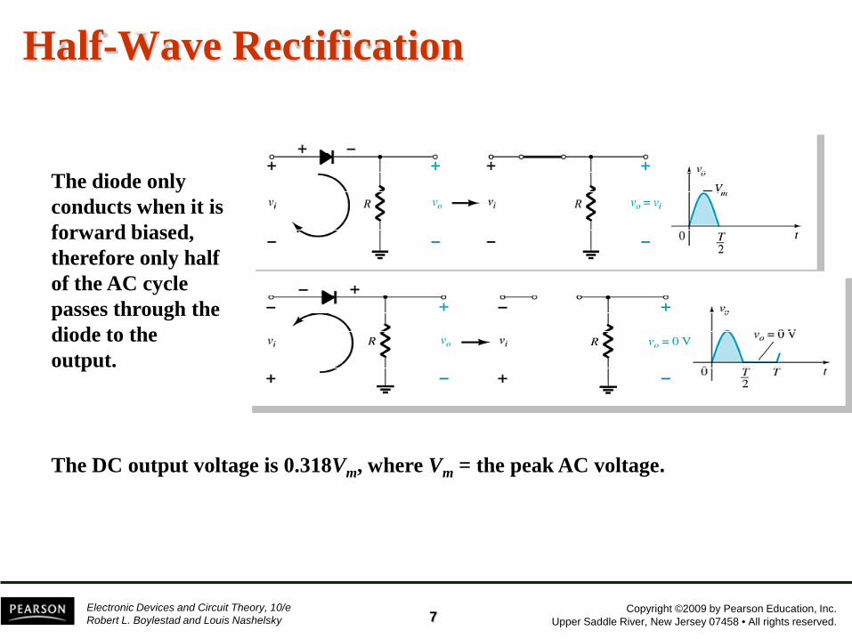
The diode only conducts when it is forward biased, therefore only half of the AC cycle passes through the diode to the output.
The DC output voltage is 0.318Vm, where Vm = the peak AC voltage.
Copyright ©2009 by Pearson Education, Inc. Upper Saddle River, New Jersey 07458 • All rights reserved.
Electronic Devices and Circuit Theory, 10/e Robert L. Boylestad and Louis Nashelsky
PIV (PRV)
8
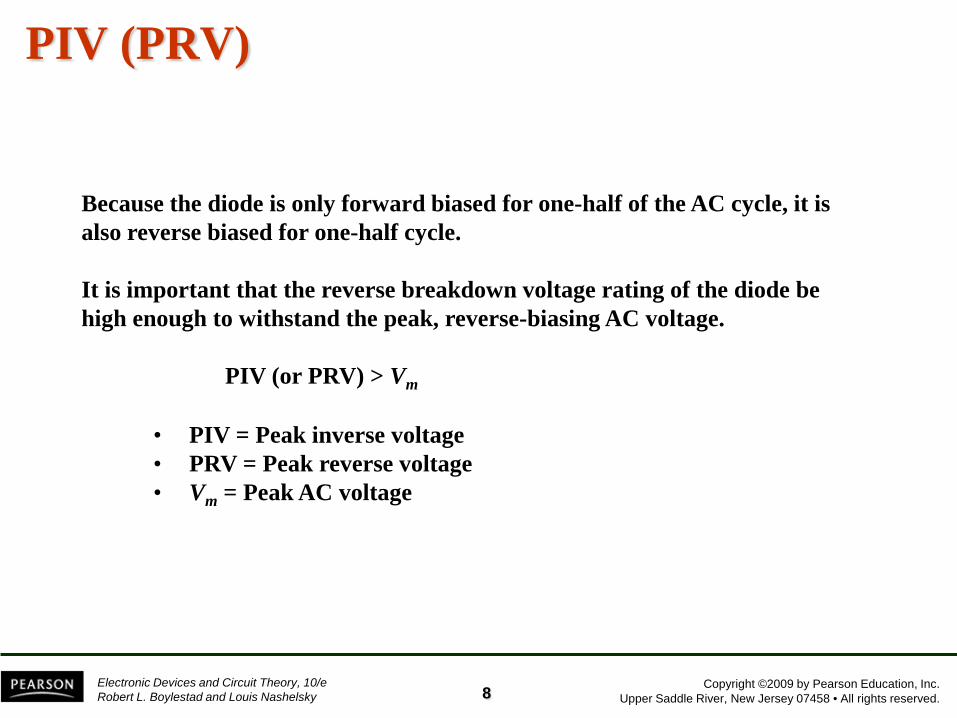
Because the diode is only forward biased for one-half of the AC cycle, it is also reverse biased for one-half cycle. It is important that the reverse breakdown voltage rating of the diode be high enough to withstand the peak, reverse-biasing AC voltage.
PIV (or PRV) > Vm
• PIV = Peak inverse voltage • PRV = Peak reverse voltage • Vm = Peak AC voltage
Copyright ©2009 by Pearson Education, Inc. Upper Saddle River, New Jersey 07458 • All rights reserved.
Electronic Devices and Circuit Theory, 10/e Robert L. Boylestad and Louis Nashelsky
Full-Wave Rectification
9
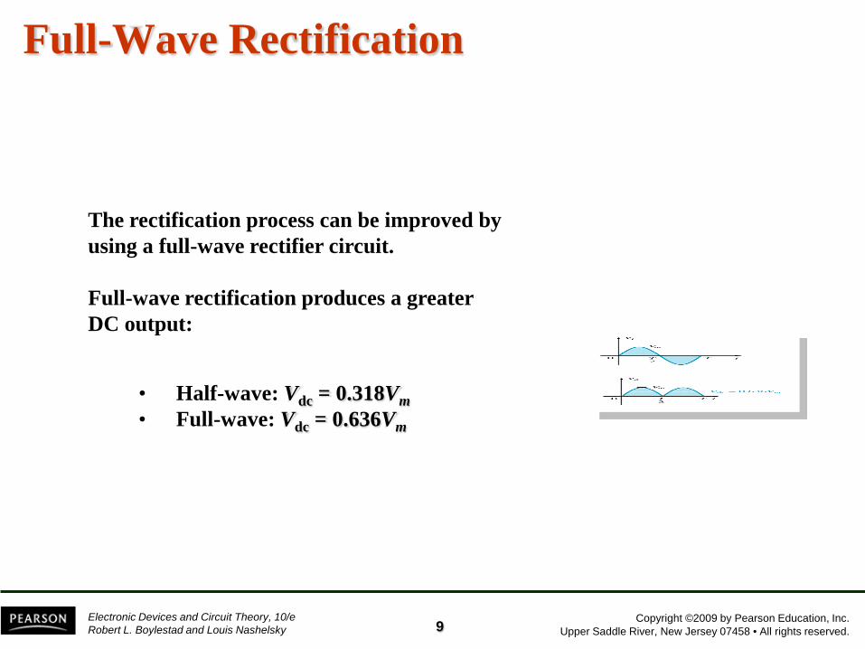
• Half-wave: Vdc = 0.318Vm • Full-wave: Vdc = 0.636Vm
The rectification process can be improved by using a full-wave rectifier circuit. Full-wave rectification produces a greater DC output:

Copyright ©2009 by Pearson Education, Inc. Upper Saddle River, New Jersey 07458 • All rights reserved.
Electronic Devices and Circuit Theory, 10/e Robert L. Boylestad and Louis Nashelsky
Full-Wave Rectification
10
Bridge Rectifier • Four diodes are connected in a
bridge configuration • VDC = 0.636Vm

Copyright ©2009 by Pearson Education, Inc. Upper Saddle River, New Jersey 07458 • All rights reserved.
Electronic Devices and Circuit Theory, 10/e Robert L. Boylestad and Louis Nashelsky
Full-Wave Rectification
11
Center-Tapped Transformer Rectifier
Requires
• Two diodes • Center-tapped transformer
VDC = 0.636Vm
Copyright ©2009 by Pearson Education, Inc. Upper Saddle River, New Jersey 07458 • All rights reserved.
Electronic Devices and Circuit Theory, 10/e Robert L. Boylestad and Louis Nashelsky
Summary of Rectifier Circuits
12
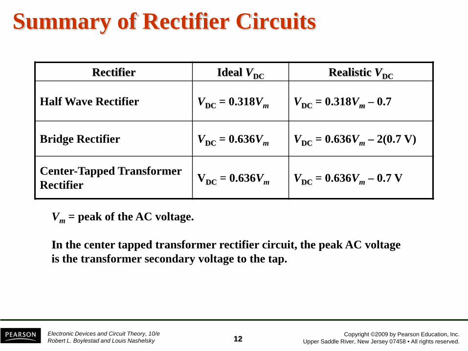
Vm = peak of the AC voltage. In the center tapped transformer rectifier circuit, the peak AC voltage is the transformer secondary voltage to the tap.
Rectifier Ideal VDC Realistic VDC
Half Wave Rectifier VDC = 0.318Vm VDC = 0.318Vm – 0.7
Bridge Rectifier VDC = 0.636Vm VDC = 0.636Vm – 2(0.7 V)
Center-Tapped Transformer Rectifier VDC = 0.636Vm VDC = 0.636Vm – 0.7 V

Copyright ©2009 by Pearson Education, Inc. Upper Saddle River, New Jersey 07458 • All rights reserved.
Electronic Devices and Circuit Theory, 10/e Robert L. Boylestad and Louis Nashelsky
Diode Clippers
•
13
The diode in a series clipper “clips” any voltage that does not forward bias it: •A reverse-biasing polarity •A forward-biasing polarity less than 0.7 V (for a silicon diode)
Copyright ©2009 by Pearson Education, Inc. Upper Saddle River, New Jersey 07458 • All rights reserved.
Electronic Devices and Circuit Theory, 10/e Robert L. Boylestad and Louis Nashelsky
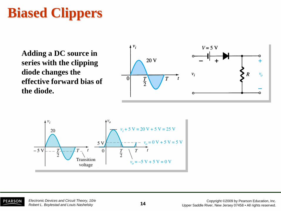
Biased Clippers
14
Adding a DC source in series with the clipping diode changes the effective forward bias of the diode.
Copyright ©2009 by Pearson Education, Inc. Upper Saddle River, New Jersey 07458 • All rights reserved.
Electronic Devices and Circuit Theory, 10/e Robert L. Boylestad and Louis Nashelsky
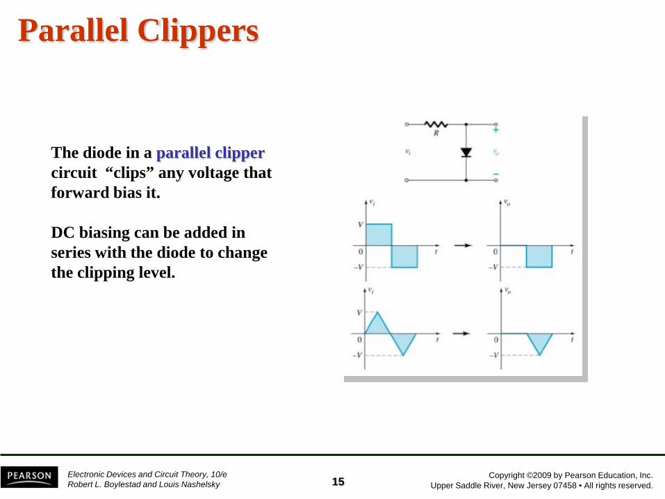
Parallel Clippers
15
The diode in a parallel clipper circuit “clips” any voltage that forward bias it. DC biasing can be added in series with the diode to change the clipping level.

Copyright ©2009 by Pearson Education, Inc. Upper Saddle River, New Jersey 07458 • All rights reserved.
Electronic Devices and Circuit Theory, 10/e Robert L. Boylestad and Louis Nashelsky
Summary of Clipper Circuits
16
more…
Copyright ©2009 by Pearson Education, Inc. Upper Saddle River, New Jersey 07458 • All rights reserved.
Electronic Devices and Circuit Theory, 10/e Robert L. Boylestad and Louis Nashelsky
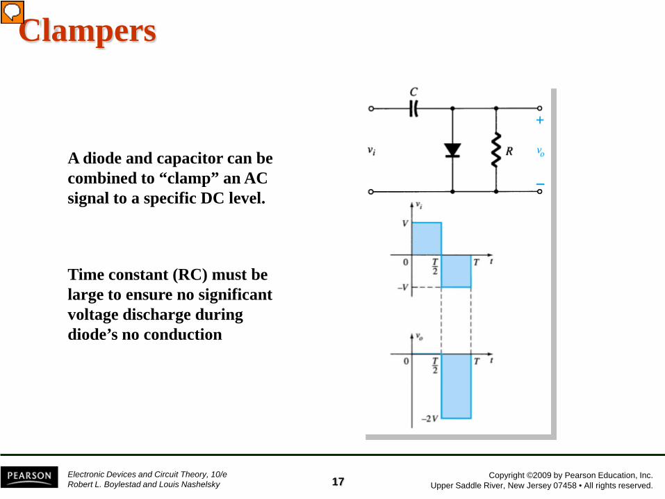
Clampers
17
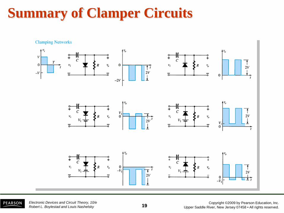
A diode and capacitor can be combined to “clamp” an AC signal to a specific DC level.
Time constant (RC) must be large to ensure no significant voltage discharge during diode’s no conduction
Copyright ©2009 by Pearson Education, Inc. Upper Saddle River, New Jersey 07458 • All rights reserved.
Electronic Devices and Circuit Theory, 10/e Robert L. Boylestad and Louis Nashelsky
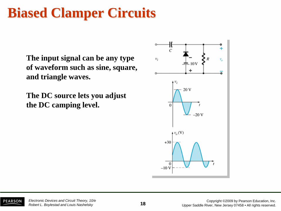
Biased Clamper Circuits
18
The input signal can be any type of waveform such as sine, square, and triangle waves. The DC source lets you adjust the DC camping level.
Copyright ©2009 by Pearson Education, Inc. Upper Saddle River, New Jersey 07458 • All rights reserved.
Electronic Devices and Circuit Theory, 10/e Robert L. Boylestad and Louis Nashelsky
Summary of Clamper Circuits
19

Copyright ©2009 by Pearson Education, Inc. Upper Saddle River, New Jersey 07458 • All rights reserved.
Electronic Devices and Circuit Theory, 10/e Robert L. Boylestad and Louis Nashelsky
Zener Diodes
20
The Zener is a diode operated in reverse bias at the Zener Voltage (Vz).
• When Vi ≥ VZ – The Zener is on – Voltage across the Zener is VZ – Zener current: IZ = IR – IRL – The Zener Power: PZ = VZIZ
• When Vi < VZ
– The Zener is off – The Zener acts as an open circuit
Copyright ©2009 by Pearson Education, Inc. Upper Saddle River, New Jersey 07458 • All rights reserved.
Electronic Devices and Circuit Theory, 10/e Robert L. Boylestad and Louis Nashelsky
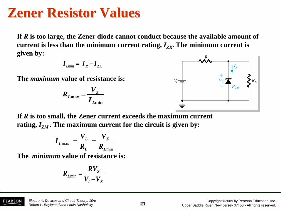
Zener Resistor Values
21
ZKRL I II −= min
minmax
L
ZL I
VR =
minmax
L
Z
L
LL R
V R
V I ==
Zi
ZL VV
RVR−
=min
If R is too large, the Zener diode cannot conduct because the available amount of current is less than the minimum current rating, IZK. The minimum current is given by:
The maximum value of resistance is:
If R is too small, the Zener current exceeds the maximum current rating, IZM . The maximum current for the circuit is given by:
The minimum value of resistance is:

Copyright ©2009 by Pearson Education, Inc. Upper Saddle River, New Jersey 07458 • All rights reserved.
Electronic Devices and Circuit Theory, 10/e Robert L. Boylestad and Louis Nashelsky
Voltage-Multiplier Circuits
• Voltage Doubler • Voltage Tripler • Voltage Quadrupler
22
Voltage multiplier circuits use a combination of diodes and capacitors to step up the output voltage of rectifier circuits.
Copyright ©2009 by Pearson Education, Inc. Upper Saddle River, New Jersey 07458 • All rights reserved.
Electronic Devices and Circuit Theory, 10/e Robert L. Boylestad and Louis Nashelsky
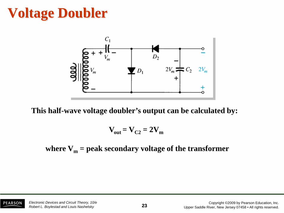
Voltage Doubler
23
This half-wave voltage doubler’s output can be calculated by:
Vout = VC2 = 2Vm
where Vm = peak secondary voltage of the transformer

Copyright ©2009 by Pearson Education, Inc. Upper Saddle River, New Jersey 07458 • All rights reserved.
Electronic Devices and Circuit Theory, 10/e Robert L. Boylestad and Louis Nashelsky
Voltage Doubler
24
• Positive Half-Cycle o D1 conducts o D2 is switched off o Capacitor C1 charges to Vm
• Negative Half-Cycle
o D1 is switched off o D2 conducts o Capacitor C2 charges to Vm
Vout = VC2 = 2Vm

Copyright ©2009 by Pearson Education, Inc. Upper Saddle River, New Jersey 07458 • All rights reserved.
Electronic Devices and Circuit Theory, 10/e Robert L. Boylestad and Louis Nashelsky
Voltage Tripler and Quadrupler
25

Copyright ©2009 by Pearson Education, Inc. Upper Saddle River, New Jersey 07458 • All rights reserved.
Electronic Devices and Circuit Theory, 10/e Robert L. Boylestad and Louis Nashelsky
Practical Applications
• Rectifier Circuits – Conversions of AC to DC for DC operated circuits – Battery Charging Circuits
• Simple Diode Circuits
– Protective Circuits against – Overcurrent – Polarity Reversal – Currents caused by an inductive kick in a relay circuit
• Zener Circuits
– Overvoltage Protection – Setting Reference Voltages
26

Copyright ©2009 by Pearson Education, Inc. Upper Saddle River, New Jersey 07458 • All rights reserved.
Electronic Devices and Circuit Theory, 10/e Robert L. Boylestad and Louis Nashelsky
Homework 2
• Load-line analysis – 2.2 (4a,4b)
• Diode Configurations – 2.4 (13)
• Rectification – 2.7 (30)
• Clippers – 2.8 (34)
• Clampers – 2.9 (40)
• Zener Diodes – 2.10 (42a)
27


![Active Subwoofer System SB-WA720PP - Philips d559 b0aack000004 diode [m] d560 b0aack000004 diode [m] d561 b0ba01200008 diode [m] d562 b0aack000004 diode [m] d563 b0ba01900005 diode](https://static.documents.pub/doc/80x56/5baed8c209d3f290738dc283/active-subwoofer-system-sb-wa720pp-philips-d559-b0aack000004-diode-m-d560-b0aack000004.jpg)


