5 Chapter 2 Fabrication of Ultra-High Density Silicon Nanowire Arrays 2.1 Introduction Nanofabrication patterning of molecules as well as metals and semiconductor structures has received increasing attention. A major challenge in the development of robust nanopatterning techniques involves the reduction of feature size and the increase in pattern density. High-density nanoscale circuits have the potential to be more efficient and faster than the conventional electronic circuits. In addition, new scientific possibilities arise when the patterning techniques begin to approach the scales and densities of macromolecules, likely offering a feasible organic-inorganic interface to biological systems. In particular, nanowire (NW) circuit fabrication has become a very active field of research. To date, NWs have been used to fabricate modular circuit elements such as field-effect transistors (FETs), 1-4 bipolar junction transistors, 5 p-n diodes, 5, 6 logic gates, 7, 8 lasers and LEDs, 9, 10 molecular memory, 11 and nanoscale electro- mechanical resonators. 12, 13 In addition to NWs, the electronic, thermal and optical properties of single-walled carbon nanotubes (SWNTs) have been extensively studied. 14, 15 In this chapter, I concentrate the discussion on the development of a robust and versatile technique to fabricate high-density silicon nanowire arrays. Significant
Transcript
5
Chapter 2 Fabrication of Ultra-High Density Silicon Nanowire Arrays 2.1 Introduction
Nanofabrication patterning of molecules as well as metals and semiconductor
structures has received increasing attention. A major challenge in the development of
robust nanopatterning techniques involves the reduction of feature size and the increase
in pattern density. High-density nanoscale circuits have the potential to be more efficient
and faster than the conventional electronic circuits. In addition, new scientific
possibilities arise when the patterning techniques begin to approach the scales and
densities of macromolecules, likely offering a feasible organic-inorganic interface to
biological systems. In particular, nanowire (NW) circuit fabrication has become a very
active field of research. To date, NWs have been used to fabricate modular circuit
elements such as field-effect transistors (FETs),1-4 bipolar junction transistors,5 p-n
diodes,5, 6 logic gates,7, 8 lasers and LEDs,9, 10 molecular memory,11 and nanoscale electro-
mechanical resonators.12, 13 In addition to NWs, the electronic, thermal and optical
properties of single-walled carbon nanotubes (SWNTs) have been extensively studied.14,
15 In this chapter, I concentrate the discussion on the development of a robust and
versatile technique to fabricate high-density silicon nanowire arrays. Significant
6
advantages afforded by such method lead to a variety of applications which are also
briefly addressed here.
Silicon is an attractive material for multiple electronic applications. The physical
and mechanical properties of silicon have been extensively studied and are well
characterized. In addition, fabrication protocols for etching, patterning and electrically
addressing silicon devices are highly developed. Finally, silicon-based devices are easily
integrated into a conventional CMOS technology, thus providing an opportunity for
large-scale manufacturing and commercialization. These reasons have sparked an
extensive research into the fabrication techniques of silicon NWs (SiNWs) and their
incorporation into functional devices. One such technique, which, at this time, is the
most widely used method of SiNW fabrication for electronic applications, is the
nanoparticle-catalyzed vapor-liquid-solid (VLS) growth mechanism.16-18 Briefly, a gold
nanocluster is heated in the presence of vapor-phase silicon (SiH4 in H2) to 362 oC, a
temperature of Au-Si eutectic, resulting in the formation of Au-Si alloy in the form of a
liquid droplet. The droplet supersaturates in Si under a continuous flow of vapor Si,
resulting in a precipitation of solid silicon. SiNW continues to grow from the solid-liquid
interface as long as the droplet is supersaturated. This process may be tuned to produce
single-crystal SiNWs with well-controlled diameter and growth orientation.19 However,
this process also has major drawbacks, which limit its usefulness as a large-scale
fabrication tool. One significant problem is the lack of precise control over the doping
level. The VLS doping is done in situ by adding dopant precursor to the reaction,
yielding NWs with doping levels and electrical properties which are largely unknown
prior to their integration into a device. Additionally, while the VLS technique allows the
7
fabrication of many NWs at once, subsequent methods are required to align NWs into
parallel arrays or crossbar circuits.17 One such method which has been the most
successful in aligning VLS grown NWs employs a Langmuir-Blodgett (LB) trough.20
Aside from being impractical for scaling up and manufacturing, LB method produces
NWs with large alignment fluctuations and poor end-to-end registry of individual NWs.
Interconnection and integration of such SiNW arrays into CMOS compatible circuitry is
difficult.
As described above, a major challenge in nanoelectronics is to be able to
reproducibly fabricate high-density NW arrays with precise control over the diameter,
length, pitch and doping level. Superlattice nanowire pattern transfer (SNAP) technique
presented here, combined with the spin-on doping method (SOD), allows such level of
control over multiple physical and electronic parameters of SiNWs, and may be extended
to the fabrication of NWs from a wide range of materials. The other challenge is higher-
order control of the device architecture, with arbitrary complex interconnections within
an array of nanostructures. While certain ordered arrangements, such as nanowire
crossbar structures,11 are useful from the point of view of electronic circuit construction,
many other applications require at least some level of nonperiodic complexity. Examples
include routing networks between nanowire field-effect transistors,4, 21 or specified
defects within photonic crystals. An extension of SNAP technique may be used to
construct arbitrarily complex, two-dimensional nanowire structures templated on a single
crystal substrate at sublithographic dimensions. As a proof-of-principle demonstration,
this method is used to construct routing networks for Si nanowire-based complementary
8
symmetry logic applications with electrical contacts which are superior to those
fabricated with other methods.
2.2 Superlattice Nanowire Pattern Transfer (SNAP)
Superlattice nanowire pattern transfer (SNAP)13 is a technique for fabricating
aligned nanowires of a wide range of materials through a one-step deposition process
without subsequent etching or liftoff, which is often necessary for other methods such as
e-beam lithography (EBL).22 These fully formed NWs may be transferred to any surface.
Further processing steps can be utilized to convert these nanowires into an identical
pattern out of a thin-film material, such as silicon on insulator (SOI). SNAP technique
has been developed to simultaneously address issues of NW size, pitch and alignment.
NWs can be fabricated from a thin film of arbitrary material, as long as dry etching of
such material is possible. Therefore, the electronic properties of the NWs produced via
SNAP may be manipulated by a corresponding control of the properties of the starting
thin film. For example, by combining SNAP technique with spin-on doping (SOD)
method, a quantitative control of the NW doping level is possible.
epitaxy (MBE) to create a physical template for NW patterning. Such template is a
GaAs/AlxGa(1-x)As superlattice structure consisting of the alternating gallium-arsenide
and aluminum-gallium-arsenide layers grown on top of a (100) GaAs substrate. The Al
mole fraction may be varied between 0.5 and 0.8. The atomic-level control over the
thickness and composition of each layer translates into atomic-level control over the
resulting metal or semiconductor nanowires. The fabrication protocol begins by dicing a
9
Figure 2.1: SNAP fabrication flow-chart. A) A small piece of the GaAs/AlGaAs superlattice is selectively etched, B, forming a comblike structure (inset: SEM image). C) Platinum is deposited at an angle along the ridges of the comb. D) The superlattice template is adhered to an epoxy-coated SOI substrate. E) The superlattice is etched away, releasing the Pt nanowires. F) Dry etch transfers the Pt NW pattern into the underlying silicon film.
portion of the superlattice wafer into 2 mm by 5 mm pieces, or masters (Figure 2.1A).
Each master has one side, {110} or {001} plane, which is atomically flat. With that side
facing up, the masters are placed into a Teflon holder and sonicated in methanol for ~10
seconds. The flat edge is swabbed until all microscopic particles are removed.
The GaAs layers are selectively etched in a solution of NH4OH/H2O2/H2O,
producing a comblike structure shown in Figures 2.1B and 2.2A. The thickness of the
AlGaAs layer determines the NW width, while the GaAs thickness translates into the
distance between the NWs. A metal, such as platinum, is then deposited at an angle
along the ridges of the AlGaAs layers on the atomically flat edge of the master (Figure
2.1C). The angle is chosen so that no metal is deposited on the etched GaAs layers, and
is, therefore, dictated by the pitch of the NWs and the depth of the grooves in the
superlattice comb structure. In general, NW pitches between 30 nm and 60 nm will
10
require a deposition angle between 45o and 15o with respect to the horizontal axis. The
thickness of the deposited metal depends on the desired width of the NWs, and is
generally 10 nm if the NW width is larger than 10 nm and equals to the NW width
otherwise.
Figure 2.2: A) Etched superlattice with comblike Al0.5Ga0.5As layers. B) Fifteen nanometers wide SiNWs. C) 20 nm wide Pt nanowires on SOI substrate. D) Twenty nanometers wide SiNWs remaining after pattern transfer of C and the removal of Pt nanowires. The scale bars and the NW pitch of B, C, and D are 50 nm and 30 nm, respectively.
The metal-coated edge of the master is gently positioned on top of the epoxy-
coated SOI surface which has been rigorously cleaned after the doping process described
below (Figure 2.1D). The epoxy is heat curable, and consists of the mixture of Epoxy
Bond 110 (Allied High Tech Products, Ranch Dominguez, CA, 10 drops part A to 1 drop
part B) and 0.15 g of 6% PMMA in 20 mL of chlorobenzene. The epoxy is spun on the
surface at 7000 RPM to form a film of approximately 10 nm thickness. Because the
11
master can be aligned on the surface at an arbitrary angle, SiNWs with crystal
orientations between (100) and (110) along the length may be produced. The master-SOI
substrate assembly is placed on the hot place at 135 oC for 45 minutes, after which it is
left in the solution of 1:5:50 (v/v/v) 30% H2O2:H3PO4:H2O for ~5 hours, until all AlGaAs
layers are etched, releasing the Pt NWs. The remaining master is detached from the
substrate and the epoxy is removed in O2 plasma. The remaining Pt nanowires (Figure
2.2C) are L shaped due to angular deposition onto the etched superlattice.
Reactive ion etching (RIE) may be used to transfer the pattern defined by the
resulting Pt nanowires into an identical pattern in the silicon epilayer of SOI substrate.
This is done with anisotropic etch in CF4/He plasma (20/30 sccm, 5 mTorr, 40 W), which
etches silicon at a rate of ~10 nm/min. Subsequently, Pt nanowires are removed in hot
aqua regia (3:1 v/v HCl:HNO3 at 120 oC for 20 minutes). As Figure 2.2 (B,D)
demonstrates, the resulting SiNWs are straight, perfectly parallel, isolated from each
other and have relatively smooth side walls. Since these wires are etched from the
epilayer of the SOI substrate, they are also electrically isolated from one another. The
procedure to convert the Si nanowires into functioning devices for biological sensing and
thermoelectric applications is described in details in the following chapters. It is critical
to emphasize the versatility afforded by the SNAP technique. First, various metal NWs
may be fabricated on any substrate; so far, the metals which have successfully yielded
NWs are gold, chromium, aluminum, titanium, niobium, platinum and nickel.13 Second,
NWs from any thin film material may be fabricated, provided that anisotropic etch for
that material exists. Third, physical parameters such as the number of parallel NWs, their
12
sizes, pitches and lengths are precisely controlled. Finally, the electronic properties of
SiNWs can be tightly modulated with quantitative doping of the initial thin silicon film.
Figure 2.3: A) An array of 1400 SiNWs 20 nm wide with 35 nm pitch. B) An array of 200 SiNWs 10 nm wide with 60 nm pitch. The inset scale bars are 100 nm.
The size of the array containing SiNWs is only limited by the MBE growth time, and
could, in principle, be increased to thousands of NWs. Figure 2.3A demonstrates the
largest array produced so far with SNAP technique, containing 1400 SiNWs with 20 nm
width. The diameter of the NWs may also, in principle, be significantly decreased to
about 1 nm or less, owing to atomic-level control of the MBE process. In practice,
however, it has been rather difficult to reproducibly obtain SiNWs thinner than ~7 nm,
although it certainly is not by any means the limit of the technique. Ten-nanometers-
13
wide NWs (Figure 2.3B) have been extensively studied in context of, for example, silicon
thermoelectric properties (chapter five).
2.3 Diffusion Doping of Silicon Thin Films
As mentioned above, a major advantage of SNAP technique is that the starting
material is a thin film, the electrical properties of which are much easier to control
through doping than those of NWs grown via VLS technique. A large SOI surface can be
uniformly doped and used to produce multiple SiNW arrays, all of which will have an
identical concentration of impurities. This allows us to carry out systematic studies of the
effects of doping concentration on, for example, the electrical and thermoelectrical
properties of NWs. These studies generally require many NW samples whose doping
levels are quantified and are the same. For this purpose we have utilized spin-on doping
(SOD) technique, which is based on the thermally mediated impurity diffusion. SOD
method has several very important advantages over other thin-film doping techniques,
such as ion implantation. Ion implantation, which uses high energy ion flux, results in
the lattice damage of the SOI substrate and the reduction the electrical conductivity of the
NWs.23 The diffusion doping process, on the other hand, does not lead to the damage of
thin silicon film. The other practical advantage of SOD technique is that the doping may
be tuned over a large range of concentrations by simply varying the temperature. This
may be readily done on small wafer pieces, introducing the flexibility which is lacking
when large wafers have to be sent out for ion implantation. In addition, patterned
diffusion doping of the thin-film substrate is necessary to create more complicated
14
circuits such as complementary logic gates, where n-type and p-type FETs must exist on
the same device in close proximity.8
The SOD procedure consists of four steps: wafer cleaning, application of the
dopant, annealing and removal of the dopant. Wafers have to be thoroughly cleaned to
remove any diffusion barriers on the surface which can result in non-uniform doping of
800 820 840 860 880 9001E14
1E15
1E16
1E17
1E18
1E19
1E20
Temperature (C)
n/p
(cm
-3 )
800 820 840 860 880 9001E14
1E15
1E16
1E17
1E18
1E19
1E20
Temperature (C)
n/p
(cm
-3 )
Figure 2.4: Impurity concentrations (cm-3) of p-type (circles) and n-type (triangles) substrates obtained from annealing at different temperatures for 3 min. After the annealing, p-type substrates were either thermally oxidized (grey circles) or simply washed with BOE (black circles).
the substrate. RCA clean is used: 5:1:1 H2O/H2O2/NH4OH for 10 min at 80oC, followed
by the removal of oxide in dilute (50:1 H2O/HF) hydrofluoric acid, followed by 6:1:1
H2O/H2O2/HCl for 10 min at 80 oC. The wafers are rinsed with H2O and a thin film of
dopants is spun on the surface. Most spin-on dopants consist of the desired species (such
as phosphorus or boron) incorporated into a silica or organic polymer matrix dissolved in
an organic solvent. For all the applications in this thesis, Boron A organic film
(Filmtronics, Bulter, PA) was used to produce p-type substrates, while phosphorosilica
(Emulsitone, Whippany, NJ) films generated n-type devices. Thin films of dopant were
15
baked on a hot plate for 10 min at 200 oC prior to the annealing. Rapid thermal annealer
(RTA) was used to precisely control the temperature and time of the annealing, which
was carried out under nitrogen. Usually, the temperature was varied and the time was
maintained at 3 min to achieve different doping concentrations. Figure 2.4 summarizes
the annealing conditions and the impurity concentrations they yield. After the annealing,
phosphorosilica film was removed simply by immersion in BOE for a few seconds,
resulting in a hydrophobic surface. Boron A film, however, could not usually be
completely removed with BOE, as indicated by the hydrophilicity of the substrate. For
applications such as biological sensing, where a hydrophobic surface is required at this
step to assure the presence of exposed oxide later for subsequent surface functionalization,
the substrates were thermally oxidized in RTP for a minute in pure oxygen at the same
temperature as the previous annealing step. After the oxidation and BOE treatment,
hydrophobic surface could be reliably obtained. The thermal oxidation, however,
somewhat lowered the impurity doping (Figure 2.4), probably because of the oxidation
and removal of the top few layers of the silicon.
The electrical resistivity of the thin film was measured with 4-point technique24
by applying a 10 mA DC current between the outer pins and measuring the voltage drop
across the inner pins. The resistivity was converted to the approximate impurity
concentration by using the reference tables generated for bulk silicon.24 The doping
profile as a function of depth into the silicon epilayer was determined experimentally
(Figure 2.5, blue triangles and red squares) by thinning a 50 nm Si epilayer in 10 nm
steps via CF4 etching, each time measuring the electrical resistivity of the film. Diffusion
16
Figure 2.5: Dopant density vs. depth for 50 nm SOI substrates with and without dopant drive-in. Si epilayers that were diffusion doped normally as described in the text (triangles and squares) show a rapid decrease in dopant density with depth as expected from calculations (dashed line). SOI subjected to an additional dopant drive-in as described in the text (circles) show a more homogeneous dopant density with depth.1
doping produces an impurity gradient which falls rapidly away from the surface. The
model of the infinitely thick Si epilayer (Figure 2.5, dashed line) agrees well with the
experimental data.1 The inhomogeneous doping profile shown in Figure 2.5 has
important implications for a variety of applications, as will be described later in this
chapter. However, there are cases when a homogeneous doping is required. An
additional annealing step is then used. The dopant film is removed as described above
and ~250 nm of SiO2 is deposited (PECVD) on the substrate. Subsequently, the wafer is
annealed at 1000 oC for 10-15 minutes to produce a homogeneous doping profile shown
in Figure 2.5 (green circles).1
17
2.4 Two-Dimensional Nanowire Circuits
As described above, high-density nanocircuits with more complex architectures
such as a crossbar are usually fabricated either using EBL or, in the case of VSI SiNWs20
or SWNTs25, 26, utilizing Langmuir-Blodgett trough technique or an AC electric field,
respectively. All these methods are serial and generally produce functional devices with
low yield, making them sufficient only for one-off demonstrations. Being a top-down
approach, SNAP may be easily extended to fabricate more complicated two-dimensional
(2D) circuits for a variety of applications. For example, the production of 2D SiNW logic
and routing circuits at sublithographic dimensions involves combining SNAP process
with other patterning techniques such as e-beam lithography (EBL). The unprecedented
dimension and density that can be achieved by the SNAP method for the production of
aligned NW arrays is complemented by the arbitrary complexity that can be achieved via
the incorporation of traditional patterning methods.
In a typical process, as demonstrated in Figure 2.6A, an array of Pt NWs is first
deposited by the SNAP technique onto an SOI substrate as described above. The
substrate is then further patterned using electron beam lithography to generate arbitrarily
complex structures on top of the first set of Pt NWs. After the evaporation and
subsequent liftoff of 20 Å Ti (as a sticking layer) and 100 Å Pt, a 2D structure consisting
of Pt NWs and perpendicular Pt bars is obtained. Pt is then used as an etch mask to
transfer the pattern into the underlying SOI epilayer via a directional dry etching with
CF4 gas. The entire process is concluded with the removal of Pt NWs and bars in aqua
regia (Figure 2.6A). The resulting 2D Si structure consists of NWs connected by arbitrary
routing bars, all formed from a single-crystalline layer of Si. Figure 2.6B shows an array
18
Figure 2.6: Two-dimensional SiNW arrays with monolithic connections. (A) Schematic illustrations of the fabrication process. Starting with Pt NWs fabricated by the SNAP method, e-beam or photolithography is used to create patterns on top of the Pt NWs (i). After metal evaporation and liftoff, a 2D Pt NW structure is formed (ii). This pattern is transferred into an SOI epilayer and the Pt mask is removed (iii). (B) An array of 400 SiNWs with monolithic connection bars. (C) An integrated inverter with SiNWs connected by monolithic bars (bottom inset). The Si/metal contacts (top inset) are between the monolithic Si bars (green) and metal leads (red). Scale bars of the insets are 500 nm.
of 400 20 nm wide SiNWs with a pitch of 33 nm. The NWs are connected by Si bars
with various widths, ranging from 50 to 500 nm. Alternatively, instead of connecting
them all at once, a subset of NWs can be selectively connected, as shown in Figure 2.6C.
This structure can be used to fabricate, among other things, integrated electronic logic
gates. The false color-coded green structures in Figure 2.6C are current routing bars,
19
which are single crystalline extensions of the SiNWs. They negate the need for direct
electrical contacts to the nanowires. The device depicted in Fig 2.6C is a complementary
symmetry inverter, or NOT gate.
The monolithic NW structure can be utilized to form high-quality and reliable
electrical contacts which are crucial for any application such as high performance NW
field effect transistors (FETs), thermoelectrics (chapter 5) or SiNW biosensors (Chapter
3). Despite enormous efforts by various researchers, obtaining reliable electrical contacts
to SiNWs ~10-20 nm wide using metal pads remains a challenge. Because of the high
surface-to-volume ratio, NWs are more sensitive to surface states than their bulk
counterparts.8, 27 Electrical contacts to the NWs, therefore, are significantly influenced by
the surface states and their quality depends on particular steps in the fabrication process,
such as contact annealing. Often, these necessary processing steps vary significantly for
n-type and p-type Si FETs. Single-crystalline, 2D SiNW circuits may represent a
universal solution to this challenging problem. First, the electrical contacts to the NWs
are established through relatively large Si pads, rather than through the NWs themselves
(Figure 2.6C). These types of metal/Si contacts are less sensitive to the surface states and
have been extensively studied and optimized for conventional MOSFET fabrication.
Second, the doping levels within contact regions and those of NWs may be separately
optimized, as described later in the text. Finally, the routing Si bars can have an
arbitrarily complex architecture (Figure 2.6C).
As described in the previous section, diffusion doping of SOI epilayer results in
an impurity gradient, with highest doping concentration at the silicon surface (Figure 2.5).
Depending on the doping conditions, the impurity density can decrease by a factor of 10
20
to 100 at a distance of ~10 nm below the top NW surface. Such sharp gradient can assist
in separately modulating the NW and contact doping levels. High impurity concentration,
in general, means that the Fermi level of the NWs is close to or in the conduction (n-type)
or the valence band (p-type). As a result, the changes in the gate potential are inadequate
to significantly alter the Fermi level, and the channel resistance of an FET does not
change appreciably, yielding a poor gate modulation. Heavily doping NWs, on the other
hand, results in a short depletion width within Si and a narrow Schottky barrier between
metal and Si. Charge transfer through the contact region is, therefore, highly efficient.
Such contact is less sensitive to the surface states due to the reduced depletion width.
Overall, a heavily doped semiconductor forms good electrical contact but does not
respond well to gate modulation. Conversely, the Fermi level of a lightly doped
semiconductor is typically in the midgap, slightly deviating toward the conduction (n-
type) or valence band (p-type). Small changes in the gate potential cause large shifts of
the Fermi level and an efficient gate modulation. However, a lower doping level also
means a longer depletion width, making the FET body very sensitive to surface and
interface states. In general, it is difficult to establish good electrical contacts to lightly
doped silicon.
An ideal FET structure exhibits different doping profiles in different regions: the
source-drain (S-D) channel is lightly doped, while the S and D contact regions are
heavily doped. Conventional FET structures are fabricated with such inhomogeneous
doping profiles, which are achieved using ion implantation methods. To avoid damaging
the NWs, alternative approaches are required to achieve similar doping profiles.23 In
meeting this challenge, various approaches have been reported. These include the
21
formation of metal silicides at the NW S and D contacts28 or synthesizing NWs with
in forming high quality contacts has not been demonstrated yet. Our approach to create
inhomogeneous doping profiles along the FET channel involves a two-step process.
FETs are first fabricated with the entire body, including the channel and
semiconductor/metal interface, doped heavily (i.e. >1019 cm-3). After the deposition of
metal contacts, anisotropic etching with CF4 gas removes the top (heavily doped) layers
of Si. Metal contacts protect the S/D silicon regions, which remain heavily doped.
Figure 2.7: Selective NW channel etching to form lightly doped devices with heavily doped contacts. (A) As-made NW FETs with heavily doped channel. Device structure is schematically shown as the inset. The current is not modulated by the sweeping of the gate voltage (VGS). (B) After the selective etching, the doping level is greatly reduced in the channel region and the FETs can be fully depleted. The contact regions are still protected by the metal, as shown in the inset.
The effect of selective CF4 etching described above is clearly demonstrated in
Figure 2.7. Initially, the devices are highly doped and the source/drain (S/D)
conductance changes little when the bottom gate is swept from -20 to 20 V (Figure 2.7A).
After the etching, the reduced channel doping level yields a much better gate modulation:
the S/D conductance changes by more than 3 orders of magnitude in the same range of
22
the gate voltage (Figure 2.7B). Importantly, this method is compatible with both p- and
n-type FETs. The development of a single process which can be applied to both p- and n-
type NW FETs is enabling for power-efficient complementary symmetry NW logic
applications.8 Alternatively, one must rely on different annealing methods or other
phenomenological treatments to get reliable contacts to NW FETs.28
Figure 2.8: SiNW FETs with monolithic and heavily doped contacts. Electrical characterization of p-type 20 nm wide NWs: (A) I-V curves at different gate potentials (from -20V to 10V, 5V increments) and (B) current as a function of VGS. (C, D) Identical electrical characterization of n-type FETs. The gate range in (C) is from 20V to -10V, with -5V increments.
Combining the selective channel etching and the monolithic structures yields high
quality electrical contacts (Figure 2.8). For both p- and n-FETs, the linear I-V behavior
23
Figure 2.9: Fabrication of a suspended SiNW array. As schematically shown in (A), monolithic contacts are formed first and the window in e-beam resist is opened around the NWs. A trench underneath the NWs is formed by etching the underlying oxide with BOE. (B) SEM image of the suspended 20 nm wide SiNWs with monolithic contacts. (C) In the absence of the monolithic Si bars, the NWs collapse into bundles.
in the low-bias regions at all measured gate potentials indicates that the contacts are
ohmic. Corresponding current versus gate voltage traces reveal that the FET conductance
can be modulated with high efficacy. Furthermore, this method is highly reliable and
reproducible. For more than 100 devices, less than twenty percent variation in the on-
current was observed from device to device.
In addition to constructing reliable, NW-based complementary symmetry logic
circuits, the 2D patterning methods can be extended towards the production of a host of
other novel and potentially useful structures as well. A first example is shown in Figure
2.9. Ultra-dense arrays of SiNWs can be suspended, thus allowing for the measurements
of thermal properties of nanowires31 or for creating high-frequency NW resonators.12
24
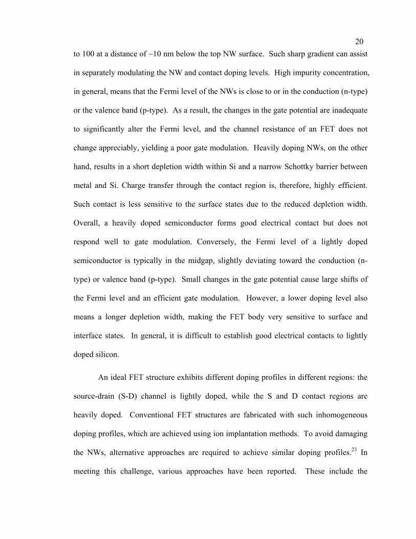
Figure 2.10: Fabrication of ultra-high density arrays of NW crossbars and holes in Si film. (A) NW crossbars are fabricated with two SNAP steps, which produce (B)two sets of NW arrays orthogonal to each other. Subsequent anisotropic dry etching (A) transfers the crossbar pattern into thin silicon epilayer, producing (C) an array of holes with ~10 nm in diameter
When an array of aligned, closely spaced NWs is suspended over a trench, various
processing steps, coupled with the van der Waals interactions between the NWs,
inevitably cause NWs to collapse into bundles (Figure 2.9B). The integrity of the
suspended NWs can be maintained by fixing them on either end with an in-plane
monolithic structure of the type described above (Figure 2.9C). Nevertheless, it is worth
pointing out that this method does have its limitations. When the trench is too wide,
proximity of the NWs still may cause them to collapse together, even in the presence of
the monolithic bars.
25
Multiple SNAP transfers can also be utilized in sequence to generate different
three-dimensional circuits. For example, two orthogonal NW arrays may be constructed
for applications in ultra-high density molecular memory based on the crossbar
architecture (Figure 2.10B).11 Crossbar devices of this type may be further used to
fabricate arrays of nanometer diameter holes in silicon with nanometer spacing (Figure
2.10). The nanohole arrays can be tuned in a number of ways. First, their diameter can
be adjusted by using NW superlattice with a different pitch. Second, the spacing between
holes can be tuned by using NWs of different widths. Third, their shape can be changed
by aligning the two sets of NW arrays at different angles. The nanohole arrays are of
some interest and potentially useful in photonic applications.32-34
2.5 Discussion
As demonstrated in this chapter, Superlattice Nanowire Pattern Transfer (SNAP)
is a very versatile technique for the fabrication of high-density nanowires from a wide
range of materials, including silicon. Important advantages of SNAP over other SiNW
fabrication methods, such as VLS technique, allow for systematic studies of the
fundamental properties of nanowires which go beyond one-off device demonstrations.
SNAP allows precise control over the number, width, spacing and length of the
nanowires. In addition, perfectly parallel arrays of NWs are fabricated, eliminating the
necessity for complicated alignment techniques such as those utilizing Langmuir-
Blodgett trough. Complicated circuits, therefore, may be readily fabricated with high
precision and yield. In addition, the top-down nature of SNAP means that the impurity
levels of NWs can be carefully controlled by standard thin-film diffusion doping methods.
As demonstrated here and in the following chapters, it is critical to be able to
26
systematically and quantitatively manipulate the dopant concentrations for optimizing the
electrical properties of SiNW-based FETs, thermoelectrics and biological sensors. Using
the traditional lithography in combination with SNAP yields 2D NW circuitry of arbitrary
complexity. Reproducibly obtaining high quality contacts to SiNWs is a major challenge.
However, by integrating an additional processing step, very high quality metal/Si
contacts to 10 nm wide SNAP NWs can be fabricated. Robustness and versatility of the
technique, ease of fabrication and the quality of the produced nanomaterial are central
issues in nanoelectronics. SNAP exhibits superior performance in each of these
categories.
27
Bibliography
1. Beckman, R.; Johnston-Halperin, E.; Luo, Y.; Green, J. E.; Heath, J. R., Bridging dimensions: Demultiplexing ultrahigh-density nanowire circuits. Science 2005, 310, (5747), 465-468.
2. Duan, X. F.; Huang, Y.; Cui, Y.; Wang, J. F.; Lieber, C. M., Indium phosphide nanowires as building blocks for nanoscale electronic and optoelectronic devices. Nature 2001, 409, (6816), 66-69.
3. Cui, Y.; Zhong, Z. H.; Wang, D. L.; Wang, W. U.; Lieber, C. M., High performance silicon nanowire field effect transistors. Nano Lett. 2003, 3, (2), 149-152.
4. Wang, D. W.; Sheriff, B. A.; Heath, J. R., Silicon p-FETs from ultrahigh density nanowire arrays. Nano Lett. 2006, 6, (6), 1096-1100.
5. Cui, Y.; Lieber, C. M., Functional nanoscale electronic devices assembled using silicon nanowire building blocks. Science 2001, 291, (5505), 851-853.
6. Huang, Y.; Duan, X. F.; Cui, Y.; Lieber, C. M., Gallium nitride nanowire nanodevices. Nano Lett. 2002, 2, (2), 101-104.
7. Huang, Y.; Duan, X. F.; Cui, Y.; Lauhon, L. J.; Kim, K. H.; Lieber, C. M., Logic gates and computation from assembled nanowire building blocks. Science 2001, 294, (5545), 1313-1317.
8. Wang, D. W.; Sheriff, B. A.; Heath, J. R., Complementary symmetry silicon nanowire logic: Power-efficient inverters with gain. Small 2006, 2, (10), 1153-1158.
9. Pauzauskie, P. J.; Sirbuly, D. J.; Yang, P. D., Semiconductor nanowire ring resonator laser. Phys. Rev. Lett. 2006, 96, (14).
11. Green, J. E.; Choi, J. W.; Boukai, A.; Bunimovich, Y.; Johnston-Halperin, E.; DeIonno, E.; Luo, Y.; Sheriff, B. A.; Xu, K.; Shin, Y. S.; Tseng, H. R.; Stoddart, J. F.; Heath, J. R., A 160-kilobit molecular electronic memory patterned at 10(11) bits per square centimetre. Nature 2007, 445, (7126), 414-417.
12. Husain, A.; Hone, J.; Postma, H. W. C.; Huang, X. M. H.; Drake, T.; Barbic, M.; Scherer, A.; Roukes, M. L., Nanowire-based very-high-frequency electromechanical resonator. Appl. Phys. Lett. 2003, 83, (6), 1240-1242.
13. Melosh, N. A.; Boukai, A.; Diana, F.; Gerardot, B.; Badolato, A.; Petroff, P. M.; Heath, J. R., Ultrahigh-density nanowire lattices and circuits. Science 2003, 300, (5616), 112-115.
14. McEuen, P. L.; Fuhrer, M. S.; Park, H. K., Single-walled carbon nanotube electronics. IEEE Trans. Nanotechnol. 2002, 1, (1), 78-85.
15. Dai, H. J., Carbon nanotubes: Opportunities and challenges. Surf. Sci. 2002, 500, (1-3), 218-241.
16. Morales, A. M.; Lieber, C. M., A laser ablation method for the synthesis of crystalline semiconductor nanowires. Science 1998, 279, (5348), 208-211.
17. Lu, W.; Lieber, C. M., Semiconductor nanowires. J. Phys. D 2006, 39, (21), R387-R406.
28
18. Yang, P. D., The chemistry and physics of semiconductor nanowires. MRS Bulletin 2005, 30, (2), 85-91.
19. Wu, Y.; Cui, Y.; Huynh, L.; Barrelet, C. J.; Bell, D. C.; Lieber, C. M., Controlled growth and structures of molecular-scale silicon nanowires. Nano Lett. 2004, 4, (3), 433-436.
20. Whang, D.; Jin, S.; Wu, Y.; Lieber, C. M., Large-scale hierarchical organization of nanowire arrays for integrated nanosystems. Nano Lett. 2003, 3, (9), 1255-1259.
21. Zhong, Z. H.; Wang, D. L.; Cui, Y.; Bockrath, M. W.; Lieber, C. M., Nanowire crossbar arrays as address decoders for integrated nanosystems. Science 2003, 302, (5649), 1377-1379.
23. Beckman, R. A.; Johnston-Halperin, E.; Melosh, N. A.; Luo, Y.; Green, J. E.; Heath, J. R., Fabrication of conducting Si nanowire arrays. J. Appl. Phys. 2004, 96, (10), 5921-5923.
24. Sze, S. M., Physics of Semiconductor Devices, 2nd ed. Taipei: John Wiley & Sons, 1981.
25. Diehl, M. R.; Yaliraki, S. N.; Beckman, R. A.; Barahona, M.; Heath, J. R., Self-assembled, deterministic carbon nanotube wiring networks. Angew. Chem., Int. Ed. 2001, 41, (2), 353.
26. Yan, Y. H.; Chan-Park, M. B.; Zhang, Q., Advances in carbon-nanotube assembly. Small 2007, 3, (1), 24-42.
27. Wang, D. W.; Chang, Y. L.; Wang, Q.; Cao, J.; Farmer, D. B.; Gordon, R. G.; Dai, H. J., Surface chemistry and electrical properties of germanium nanowires. J. Am. Chem. Soc. 2004, 126, (37), 11602-11611.
28. Weber, W. M.; Geelhaar, L.; Graham, A. P.; Unger, E.; Duesberg, G. S.; Liebau, M.; Pamler, W.; Cheze, C.; Riechert, H.; Lugli, P.; Kreupl, F., Silicon-nanowire transistors with intruded nickel-silicide contacts. Nano Lett. 2006, 6, (12), 2660-2666.
29. Yang, C.; Barrelet, C. J.; Capasso, F.; Lieber, C. M., Single p-type/intrinsic/n-type silicon nanowires as nanoscale avalanche photodetectors. Nano Lett. 2006, 6, (12), 2929-2934.
30. Yang, C.; Zhong, Z. H.; Lieber, C. M., Encoding electronioc properties by synthesis of axial modulation-doped silicon nanowires. Science 2005, 310, (5752), 1304-1307.
31. Li, D.; Wu, Y.; Kim, P.; Shi, L.; Yang, P.; Majumdar, A., Thermal conductivity of individual silicon nanowires. Appl. Phys. Lett. 2003, 83, (14), 2934-2936.
32. Joannopoulos, J. D.; Villeneuve, P. R.; Fan, S. H., Photonic crystals: Putting a new twist on light. Nature 1997, 386, (6621), 143-149.
33. Qiu, M.; He, S. L., Large complete band gap in two-dimensional photonic crystals with elliptic air holes. Phys. Rev. B 1999, 60, (15), 10610-10612.
34. Yablonovitch, E., Photonic band-gap structures. J. Optic. Soc. Am. B 1993, 10, (2), 283-295.