Chapter 4 : TUNED CIRCUITS Frequency selectivity is a fundamental concept in electronic communications. Communicating in a particular frequency band requires the ability of confining the signals into that band. Any filter is a frequency selective circuit. Tuned circuits are the most commonly used frequency selective circuits.
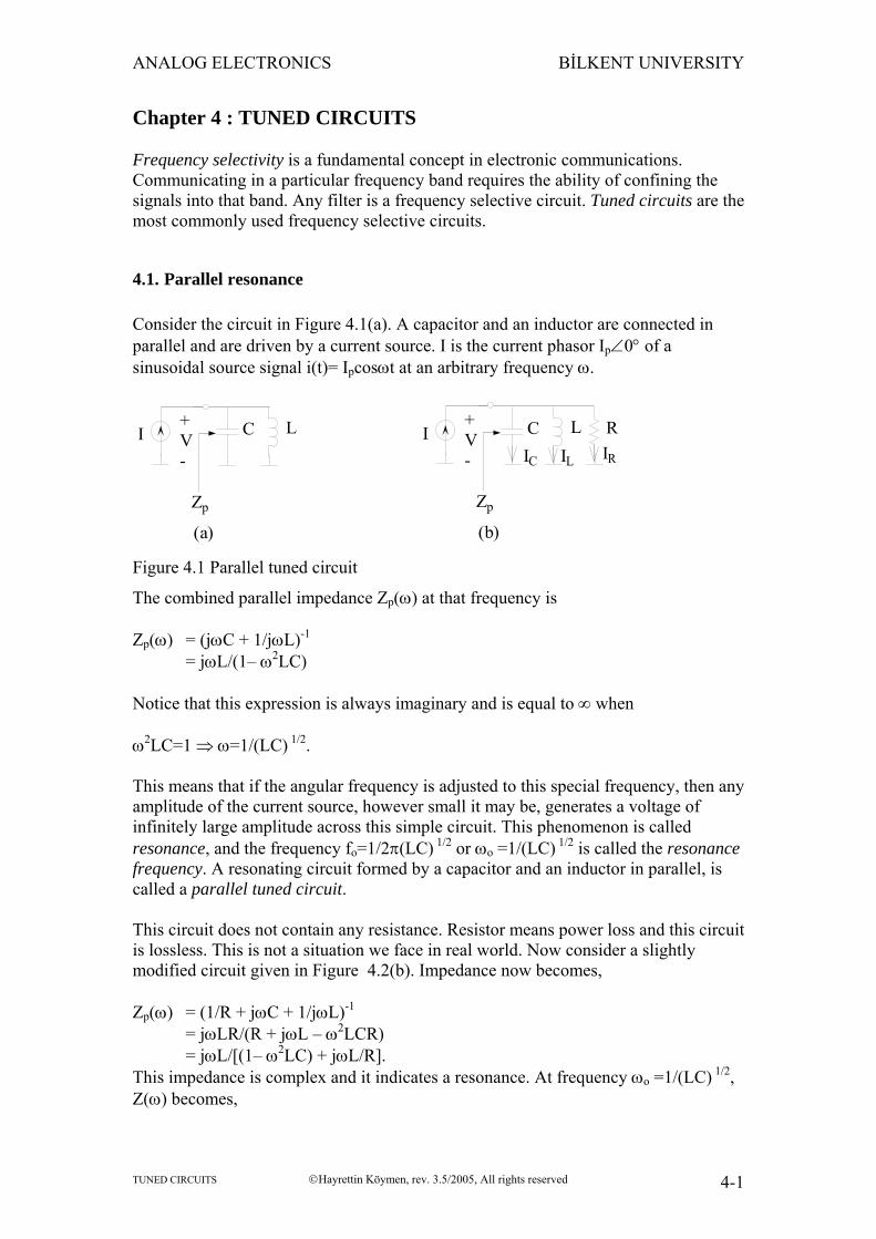
4.1. Parallel resonance Consider the circuit in Figure 4.1(a). A capacitor and an inductor are connected in parallel and are driven by a current source. I is the current phasor Ip∠0° of a sinusoidal source signal i(t)= Ipcosωt at an arbitrary frequency ω.
C L+V-
I
Zp
(a)
C L+V-
IILIC
Zp
(b)
IR
R
Figure 4.1 Parallel tuned circuit
The combined parallel impedance Zp(ω) at that frequency is Zp(ω) = (jωC + 1/jωL)-1
= jωL/(1– ω2LC) Notice that this expression is always imaginary and is equal to ∞ when ω2LC=1 ⇒ ω=1/(LC) 1/2. This means that if the angular frequency is adjusted to this special frequency, then any amplitude of the current source, however small it may be, generates a voltage of infinitely large amplitude across this simple circuit. This phenomenon is called resonance, and the frequency fo=1/2π(LC) 1/2 or ωo =1/(LC) 1/2 is called the resonance frequency. A resonating circuit formed by a capacitor and an inductor in parallel, is called a parallel tuned circuit. This circuit does not contain any resistance. Resistor means power loss and this circuit is lossless. This is not a situation we face in real world. Now consider a slightly modified circuit given in Figure 4.2(b). Impedance now becomes, Zp(ω) = (1/R + jωC + 1/jωL)-1
= jωLR/(R + jωL – ω2LCR) = jωL/[(1– ω2LC) + jωL/R]. This impedance is complex and it indicates a resonance. At frequency ωo =1/(LC) 1/2, Z(ω) becomes,
Zp(ωo) = jωoL/[(0) + jωoL/R] = R. The imaginary part of the impedance vanishes at resonance. We already know that if there would not be any resistance at all, the remaining parallel LC-circuit has infinite impedance at ωo. Infinitely large impedance in parallel with R yields R. Hence the voltage across the circuit at ω = ωo is V= IR where V is the output voltage phasor. This means that the current through the resistor is exactly equal to the input current at resonance frequency, i.e. at ω= ωo IR = I. Consider the other branch currents now. Since the voltage across the circuit is V= IR, the current in the capacitor branch is IC = IR/(1/ jωoC) = I (jωoCR). Substituting the value of ωo into above expression, capacitor current phasor at resonance frequency becomes, IC = I (jR)×(C/L) 1/2. Although there is no net current flowing into parallel LC at ωo, there is a finite current flowing through the capacitor. This current is purely imaginary. Its magnitude is determined by the component values as R(C/L) ½ times the input current and can be very large. This is a very interesting property of resonating circuits. Similarly, the current phasor of inductor branch at resonance frequency is IL = IR/(jωoL) = I (– jR/ωoL) = I (– jR)×(C/L) 1/2. Again there is a finite and imaginary current flowing through the inductor. But notice that its magnitude is exactly equal to that of IC and its phase is exactly 180o out of phase with IC, i.e. it is in exactly the opposite direction. Hence, when we add up the total current at the node joining L and C, IC and IL sums up to zero and we are left with I = IR only, at resonance. Resonance is a peculiar phenomenon!
4.1.1. Energy in tuned circuits It is shown in Section 2.3.1 that the energy stored in a capacitor at any time t1, is given as
E = C v2(t1)/2 where C is the capacitance and v(t) is the voltage across the capacitor. Similarly the energy stored in an inductor is given as E = L i2
L(t1)/2 in Section 2.5, where L is the inductance and iL(t) is the current through the inductor. The voltage v(t) across the capacitor in the circuit of Figure 4.1(b) is v(t) = IpR cos(ωot), at resonance. The stored energy in this capacitor is EC = (C/2)[ IpR cos(ωot)]2 = (C/2)[(IpR)2/2][1+cos(2ωot)]. The average value of the stored energy can be found from above expression as EavC = C (IpR)2/4 and the peak stored energy in the capacitor as EpeakC = C (IpR)2/2. Similarly, the energy stored in the inductor in the same circuit can be found from the inductor current. The inductor current phasor is Ip(-jR/ωoL), or Ip(R/ωoL) ∠-90°, which yields an inductor current iL(t) of iL(t) = Ip(R/ωoL) cos(ωot – 90°) = Ip(R/ωoL) sin(ωot). The stored energy in the inductor becomes EL = L i2
L(t1)/2 = (L/2) [Ip(R/ωoL)]2(1/2)[1 − cos(2ωot)]. The average and peak stored energy in the inductor are EavL = L [Ip(R/ωoL)]2/4 and EpeakL = L [Ip(R/ωoL)]2/2, respectively. In any one of the reactive components, C and L, in this parallel tuned circuit, the stored average energy is half of stored peak energy. Since (ωo
2L)-1 is equal to C at resonance, we can write EavL and EpeakL as EavL = [Ip
2(R2C)] /2 = EpeakC, respectively. Therefore, both the average and peak stored energy in these components are equal in parallel tuned circuit. A closer examination of time dependent expressions for energy in either component reveals that when the stored energy in one of them reaches to a maximum, the stored energy in the other becomes zero. It is useful to find the total stored energy Eav in the circuit: Eav = EavC + EavL = [Ip
2(R2C)] /2, which is equal to the peak stored energy in either component. As a matter of fact, when the stored energy in both components EC and EL are summed up at any time instant, the total stored energy Es in the circuit also becomes Es = C (IpR)2 /2.
4.1.2. Quality of resonance Quality of a resonating circuit is defined as the ratio of the stored energy in the circuit to the dissipated energy during (1/ωo) seconds. The dissipated power is, of course, the power delivered to the resistor, Pd = IR 2R/2 = Ip
2R/2, and the dissipated energy during (1/ωo) seconds is, Ed = Ip
2R/(2ωo). The quality factor is, Q = Es/ Ed
= ωoCR = R/ωoL
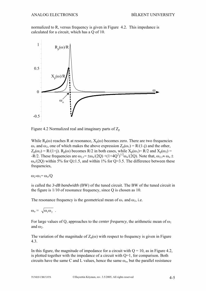
for a parallel RLC circuit. Consider the impedance expression for the RLC-circuit of Figure 4.1(b), Zp(ω) = jωL/[(1-ω2LC) + jωL/R]. After a little complex algebra, this can be written as, Zp(ω) = R/[1+jQ(ω/ωo-ωo/ω)], in terms of R, Q and ωo. We can see that when ω = ωo, |Zp(ω)| reaches a maximum at Zp(ω)=R and as frequency deviates from ωo, |Zp(ω)| decreases. The real and imaginary parts [Zp(ω)=Rp(ω)+jXp(ω)] of the impedance of a parallel circuit,
normalized to R, versus frequency is given in Figure 4.2. This impedance is calculated for a circuit, which has a Q of 10.
Rp(ω)/R
Xp(ω)/R
ω
1
0.5
-0.5
0
ωο
Figure 4.2 Normalized real and imaginary parts of Zp
While Rp(ω) reaches R at resonance, Xp(ω) becomes zero. There are two frequencies ω1 and ω2, one of which makes the above expression Zp(ω1) = R/(1-j) and the other, Zp(ω2) = R/(1+j). Rp(ω) becomes R/2 in both cases, while Xp(ω1)= R/2 and Xp(ω2) = -R/2. These frequencies are ω2,1= ±ωo/(2Q) +(1+4Q2)1/2ωo/(2Q). Note that, ω2,1≈ ωo ± ωo/(2Q) within 5% for Q≥1.5, and within 1% for Q>3.5. The difference between these frequencies, ω2-ω1= ωo/Q is called the 3-dB bandwidth (BW) of the tuned circuit. The BW of the tuned circuit in the figure is 1/10 of resonance frequency, since Q is chosen as 10. The resonance frequency is the geometrical mean of ω1 and ω2, i.e. ωo = 21ωω . For large values of Q, approaches to the center frequency, the arithmetic mean of ω1 and ω2. The variation of the magnitude of Zp(ω) with respect to frequency is given in Figure 4.3. In this figure, the magnitude of impedance for a circuit with Q = 10, as in Figure 4.2, is plotted together with the impedance of a circuit with Q=1, for comparison. Both circuits have the same C and L values, hence the same ωo, but the parallel resistance
of the high-Q circuit is 10 times larger than the other one. Note that |Zp(ω)| is R/ 2 ≈ 0.7R at ω1 and ω2, rather than R/2. The ratio of the voltage magnitudes generated across the circuit in Figure 4.1(b) at resonance and at ω1 (or ω2) is, |V(ωo)|/|V(ω1)| = |Zp(ωo)|/|Zp(ω1)| = 2 and 20log|V(ωo)/V(ω1)| ≈ 3 dB.
0
1
7
10|Zp(ω)|
Q=10
Q=1BW for Q=10
BW for Q=1
ω
Figure 4.3 |Z(ω)p| of two parallel tuned circuits
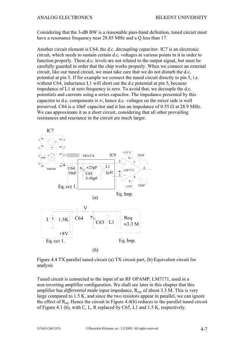
This is why the bandwidth between ω1 and ω2 is called 3-dB BW. TRC-10 employs a parallel tuned circuit in its transmitter. C65 and L1 are the components that form the resonating part. This part of the circuit is given in Figure 4.4(a). We discuss mixers in detail in Chapter 7. For the moment, we state that the equivalent circuit seen looking into the output pin 5 (or 4) of mixer chip, IC7 (SA602A or SA612A), can be well approximated by a parallel combination of a current source and a resistance of 1.5K. This circuit is depicted in Figure 4.4(b) as Eq.cct.1. IC7 is TX mixer in Figure 1.11, and the signal at the output is as given in Figure 1.13. We want to eliminate the signal components around fIF-fVFO and preserve the ones near fIF + fVFO. fIF is 16 MHz and fVFO is between 12 to 13.7 MHz, making fIF + fVFO anywhere between 28 and 29.7MHz. In order that this tuned circuit preserves the wanted signal, it must have a minimum pass-band that covers 28-29.7 MHz band.
Considering that the 3-dB BW is a reasonable pass-band definition, tuned circuit must have a resonance frequency near 28.85 MHz and a Q less than 17. Another circuit element is C64, the d.c. decoupling capacitor. IC7 is an electronic circuit, which needs to sustain certain d.c. voltages at various points in it in order to function properly. These d.c. levels are not related to the output signal, but must be carefully guarded in order that the chip works properly. When we connect an external circuit, like our tuned circuit, we must take care that we do not disturb the d.c. potential at pin 5. If for example we connect the tuned circuit directly to pin 5, i.e. without C64, inductance L1 will short out the d.c potential at pin 5, because impedance of L1 at zero frequency is zero. To avoid that, we decouple the d.c. potentials and currents using a series capacitor. The impedance presented by this capacitor to d.c. components is ∞, hence d.c. voltages on the mixer side is well preserved. C64 is a 10nF capacitor and it has an impedance of 0.55 Ω at 28.9 MHz. We can approximate it as a short circuit, considering that all other prevailing resistances and reactance in the circuit are much larger.
Tuned circuit is connected to the input of an RF OPAMP, LM7171, used in a non-inverting amplifier configuration. We shall see later in this chapter that this amplifier has differential mode input impedance, Req, of about 3.3 M. This is very large compared to 1.5 K, and since the two resistors appear in parallel, we can ignore the effect of Req. Hence the circuit in Figure 4.4(b) reduces to the parallel tuned circuit of Figure 4.1 (b), with C, L, R replaced by C65, L1 and 1.5 K, respectively.
Recall that we require a resonance frequency of 28.85 MHz and a Q less than 17. Q of this circuit is, Q = 1.5 K/ωoL = 8.3 < 17. L1 is set to 1µH. To resonate at 28.9 MHz approximately, the total capacitance across it must be about 30 pF. We must expect few picofarad parallel capacitance at mixer output and at OPAMP input, which are called stray capacitances and are due to simple physical distances. In order to set the resonance frequency we must adjust the total parallel capacitance (including stray capacitances) to 30 pF. We do this by adjusting the variable capacitor C65 to the correct value. Adjusting the capacitance to resonate the circuit at the specified frequency is called, tuning the circuit, and the capacitor is called the tuning capacitor. Quite often resonant circuits are called tuned circuits.
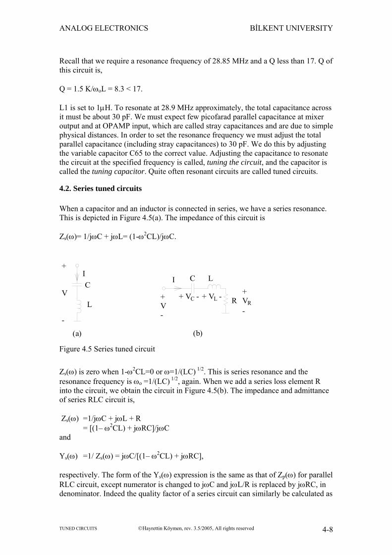
4.2. Series tuned circuits When a capacitor and an inductor is connected in series, we have a series resonance. This is depicted in Figure 4.5(a). The impedance of this circuit is Zs(ω)= 1/jωC + jωL= (1-ω2CL)/jωC.
C
L
+
V
-
I
(a)
C L
+V-
I
(b)
R+VR-
+ VC - + VL -
Figure 4.5 Series tuned circuit
Zs(ω) is zero when 1-ω2CL=0 or ω=1/(LC) 1/2. This is series resonance and the resonance frequency is ωo =1/(LC) 1/2, again. When we add a series loss element R into the circuit, we obtain the circuit in Figure 4.5(b). The impedance and admittance of series RLC circuit is, Zs(ω) =1/jωC + jωL + R = [(1– ω2CL) + jωRC]/jωC and Ys(ω) =1/ Zs(ω) = jωC/[(1– ω2CL) + jωRC], respectively. The form of the Ys(ω) expression is the same as that of Zp(ω) for parallel RLC circuit, except numerator is changed to jωC and jωL/R is replaced by jωRC, in denominator. Indeed the quality factor of a series circuit can similarly be calculated as
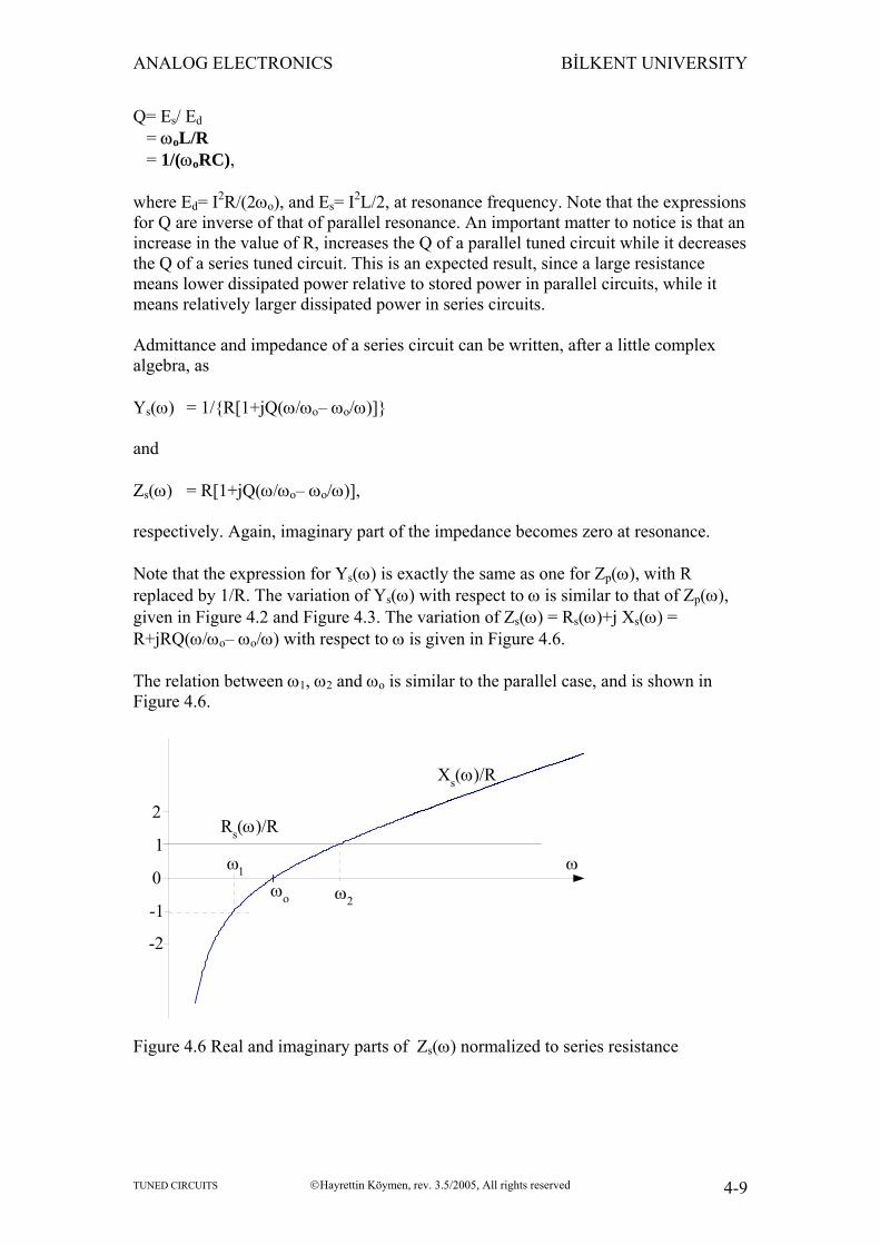
= ωoL/R = 1/(ωoRC), where Ed= I2R/(2ωo), and Es= I2L/2, at resonance frequency. Note that the expressions for Q are inverse of that of parallel resonance. An important matter to notice is that an increase in the value of R, increases the Q of a parallel tuned circuit while it decreases the Q of a series tuned circuit. This is an expected result, since a large resistance means lower dissipated power relative to stored power in parallel circuits, while it means relatively larger dissipated power in series circuits. Admittance and impedance of a series circuit can be written, after a little complex algebra, as Ys(ω) = 1/R[1+jQ(ω/ωo– ωo/ω)] and Zs(ω) = R[1+jQ(ω/ωo– ωo/ω)], respectively. Again, imaginary part of the impedance becomes zero at resonance. Note that the expression for Ys(ω) is exactly the same as one for Zp(ω), with R replaced by 1/R. The variation of Ys(ω) with respect to ω is similar to that of Zp(ω), given in Figure 4.2 and Figure 4.3. The variation of Zs(ω) = Rs(ω)+j Xs(ω) = R+jRQ(ω/ωo– ωo/ω) with respect to ω is given in Figure 4.6. The relation between ω1, ω2 and ωo is similar to the parallel case, and is shown in Figure 4.6.
1
2
0
-2
ωο
ω
Rs(ω)/R
Xs(ω)/R
-1
ω1
ω2
Figure 4.6 Real and imaginary parts of Zs(ω) normalized to series resistance
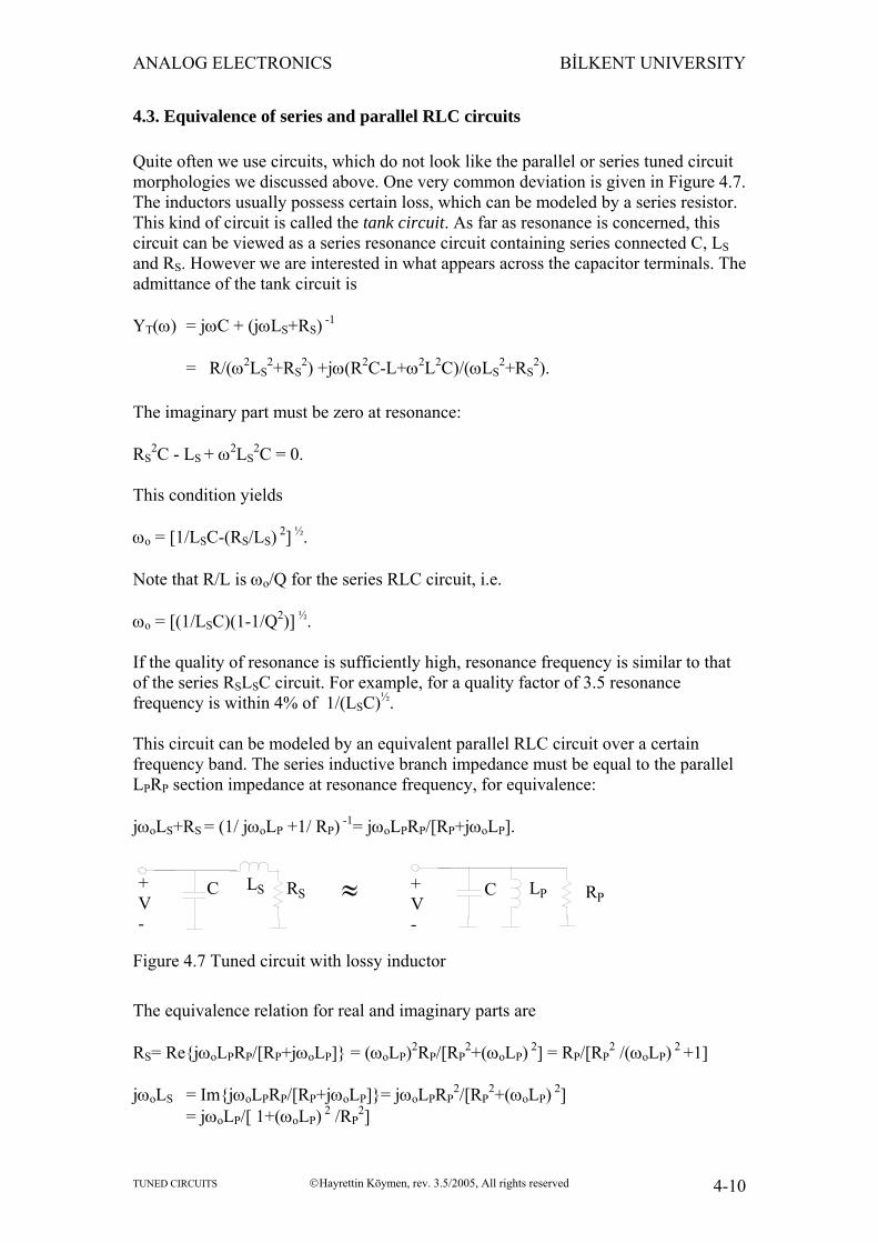
4.3. Equivalence of series and parallel RLC circuits Quite often we use circuits, which do not look like the parallel or series tuned circuit morphologies we discussed above. One very common deviation is given in Figure 4.7. The inductors usually possess certain loss, which can be modeled by a series resistor. This kind of circuit is called the tank circuit. As far as resonance is concerned, this circuit can be viewed as a series resonance circuit containing series connected C, LS and RS. However we are interested in what appears across the capacitor terminals. The admittance of the tank circuit is YT(ω) = jωC + (jωLS+RS) -1 = R/(ω2LS
2+RS2) +jω(R2C-L+ω2L2C)/(ωLS
2+RS2).
The imaginary part must be zero at resonance: RS
2C - LS + ω2LS2C = 0.
This condition yields ωo = [1/LSC-(RS/LS) 2] ½. Note that R/L is ωo/Q for the series RLC circuit, i.e. ωo = [(1/LSC)(1-1/Q2)] ½. If the quality of resonance is sufficiently high, resonance frequency is similar to that of the series RSLSC circuit. For example, for a quality factor of 3.5 resonance frequency is within 4% of 1/(LSC)½. This circuit can be modeled by an equivalent parallel RLC circuit over a certain frequency band. The series inductive branch impedance must be equal to the parallel LPRP section impedance at resonance frequency, for equivalence: jωoLS+RS = (1/ jωoLP +1/ RP) -1= jωoLPRP/[RP+jωoLP].
+V-
C LS RS ≈ C LP+V-
RP
Figure 4.7 Tuned circuit with lossy inductor
The equivalence relation for real and imaginary parts are RS= RejωoLPRP/[RP+jωoLP] = (ωoLP)2RP/[RP
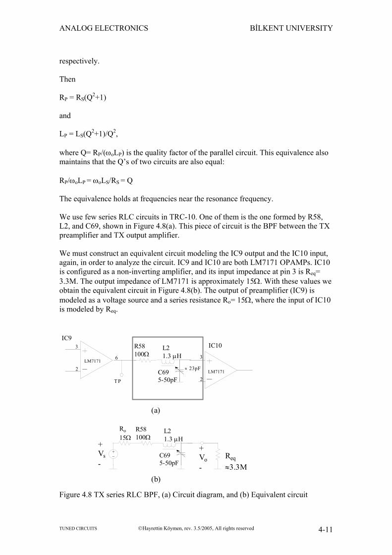
respectively. Then RP = RS(Q2+1) and LP = LS(Q2+1)/Q2, where Q= RP/(ωoLP) is the quality factor of the parallel circuit. This equivalence also maintains that the Q’s of two circuits are also equal: RP/ωoLP = ωoLS/RS = Q The equivalence holds at frequencies near the resonance frequency. We use few series RLC circuits in TRC-10. One of them is the one formed by R58, L2, and C69, shown in Figure 4.8(a). This piece of circuit is the BPF between the TX preamplifier and TX output amplifier. We must construct an equivalent circuit modeling the IC9 output and the IC10 input, again, in order to analyze the circuit. IC9 and IC10 are both LM7171 OPAMPs. IC10 is configured as a non-inverting amplifier, and its input impedance at pin 3 is Req= 3.3M. The output impedance of LM7171 is approximately 15Ω. With these values we obtain the equivalent circuit in Figure 4.8(b). The output of preamplifier (IC9) is modeled as a voltage source and a series resistance Ro= 15Ω, where the input of IC10 is modeled by Req.
T P
L21.3 µH
R58100Ω
C695-50pF
LM7171
3
2
≈ 23pF
IC10IC9
LM7171
3
2
6
(a)
C695-50pF
+_
L21.3 µH
R58100Ω
+Vo-
Req≈3.3M
Ro
15Ω
(b)
+Vs-
Figure 4.8 TX series RLC BPF, (a) Circuit diagram, and (b) Equivalent circuit
Assuming that the quality factor of this circuit is sufficiently high, the resonance frequency is approximately (1/L2C69)½. L2 and C69 must resonate at 28.9MHz, hence C69 = 1/ωo
2L2 ≈ 23 pF. The total series resistance RS and Q of the series circuit are RS= Ro + R58 = 115Ω, and Q= ωoL2/ RS ≈ 2, respectively. We need to know the magnitude of the signal applied to the amplifier input. This is the voltage across C69. The parallel equivalent resistance of RS in the tank circuit (Vs killed) is RS(Q2+1), or 575 Ω approximately. This resistance is in parallel with Req, and together they yield RS(Q2+1)// Req ≈ 575 Ω! The input impedance of IC10, Req, behaves like an open circuit compared to RS(Q2+1), and we can ignore it. Then the current in the circuit is I = Vs/(Ro + R58) at resonance and, Vo = I/(jωoC69) = Vs/ [jωoC69( Ro + R58)] = – j2 Vs. The voltage magnitude across the capacitor is twice the magnitude of the input voltage. The input voltage is effectively amplified, at the expense of increased equivalent resistance. This is a very important property of series tuned circuits. Indeed, capacitor or inductor branch voltage magnitudes are always Q times the input voltage in series RLC circuits, similar to the branch currents in parallel RLC circuits.
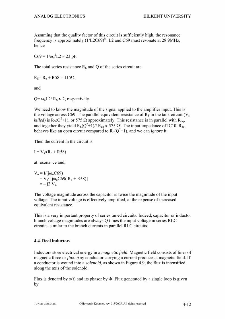
4.4. Real inductors Inductors store electrical energy in a magnetic field. Magnetic field consists of lines of magnetic force or flux. Any conductor carrying a current produces a magnetic field. If a conductor is wound into a solenoid, as shown in Figure 4.9, the flux is intensified along the axis of the solenoid. Flux is denoted by φ(t) and its phasor by Φ. Flux generated by a single loop is given by
Φl = ALI and by a solenoid of N turns is given by Φ = NΦl =NALI
FluxSolenoid
I7 turns
Figure 4.9 Inductor with 7-turn solenoidal wound conductor.
where I is the current carried by the conductor and AL is the inductance constant. The voltage generated across one loop, v1(t) and its phasor V1, by this flux are v1(t) = dφ/dt and V1 = jωΦ, respectively. There are N loops in the solenoid and they are all in series. We must add all single loop voltages up to obtain the voltage, V, across the solenoid: V= NV1
= jωNΦ = jωN2ALI The inductance of a solenoid is, therefore, L = N2AL.
The inductance constant AL depends on the size (e.g. diameter) of the loops and the type of the core, material on which the conductor is wound. Typical cores used for making inductors and transformers are: a. air, b. stacks of laminated steel sheets, c. various ferrite compounds (cores shaped as rods, beads, toroids, many other
forms), d. powdered iron based ceramics (similar to ferrites but for higher frequencies). The laminated steel core is used for mains transformers and audio applications. The core of the mains transformer we used for power supply is laminated steel type. Other three types are used for higher frequencies.
4.4.1. Air core inductors L6 and L7 in TRC-10 are air-core inductors. The easy way of designing an air-core inductor is to use the following formula, which gives the inductance value in terms of physical dimensions: L (µH) = d2N2/(46d+102l) where L is the inductance value in µH, d is coil diameter in cm, N is number of turns and l is the length of the coil in cm. This formula is quite accurate for coils having an aspect ratio l/d greater than 0.4. Let us try to find the number of turns and the dimensions for a 0.33 µH inductor. There are many choices for dimensions. Let us choose a coil geometry such that the length of the coil is equal to its diameter, i.e., l = d. Then, for 0.33 µH inductor, N2d= 48.84 cm-turns2. If we wish to have an inductor of length (and diameter in this case) 5mm, then number of turns becomes, N ≈ 10 turns. Once it is wound, the value of an air-core inductor can be tuned within about 20%, by extending its length. As the length is increased, inductance falls. Inductance of a coil increases, on the other hand, as the diameter increases or as the number of turns increases.
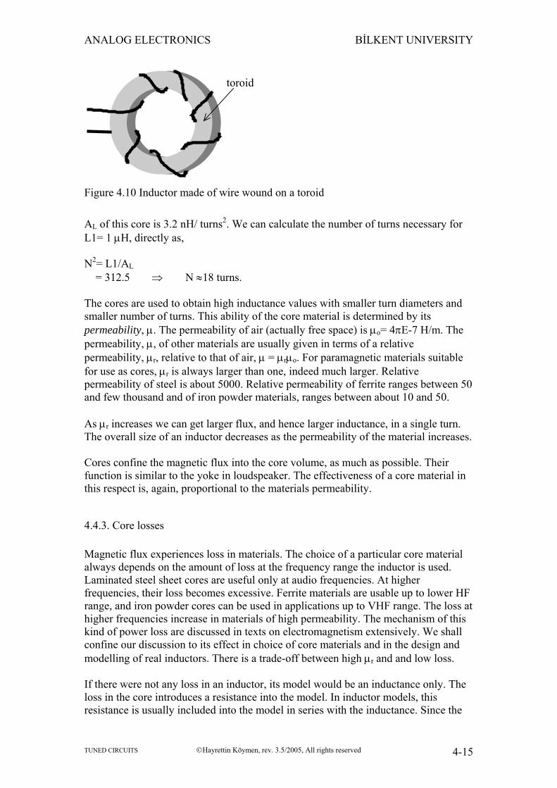
4.4.2. Powdered iron core inductors Another inductance in TRC-10 is L1. We use an iron powder core of toroidal shape for this inductor. Such an inductor is shown in Figure 4.10. The core is Micrometals T37-7. Micrometals is the company producing the core, “T” stands for toroid, “37” tells that the outer diameter of the toroid is 0.37 inch and “7” tells that the core is made of mix-7, Carbonyl-TH. The data sheet of this core is given in Appendix D.
Figure 4.10 Inductor made of wire wound on a toroid
AL of this core is 3.2 nH/ turns2. We can calculate the number of turns necessary for L1= 1 µH, directly as, N2= L1/AL
= 312.5 ⇒ N ≈18 turns. The cores are used to obtain high inductance values with smaller turn diameters and smaller number of turns. This ability of the core material is determined by its permeability, µ. The permeability of air (actually free space) is µo= 4πE-7 H/m. The permeability, µ, of other materials are usually given in terms of a relative permeability, µr, relative to that of air, µ = µrµo. For paramagnetic materials suitable for use as cores, µr is always larger than one, indeed much larger. Relative permeability of steel is about 5000. Relative permeability of ferrite ranges between 50 and few thousand and of iron powder materials, ranges between about 10 and 50. As µr increases we can get larger flux, and hence larger inductance, in a single turn. The overall size of an inductor decreases as the permeability of the material increases. Cores confine the magnetic flux into the core volume, as much as possible. Their function is similar to the yoke in loudspeaker. The effectiveness of a core material in this respect is, again, proportional to the materials permeability.
4.4.3. Core losses Magnetic flux experiences loss in materials. The choice of a particular core material always depends on the amount of loss at the frequency range the inductor is used. Laminated steel sheet cores are useful only at audio frequencies. At higher frequencies, their loss becomes excessive. Ferrite materials are usable up to lower HF range, and iron powder cores can be used in applications up to VHF range. The loss at higher frequencies increase in materials of high permeability. The mechanism of this kind of power loss are discussed in texts on electromagnetism extensively. We shall confine our discussion to its effect in choice of core materials and in the design and modelling of real inductors. There is a trade-off between high µr and and low loss. If there were not any loss in an inductor, its model would be an inductance only. The loss in the core introduces a resistance into the model. In inductor models, this resistance is usually included into the model in series with the inductance. Since the
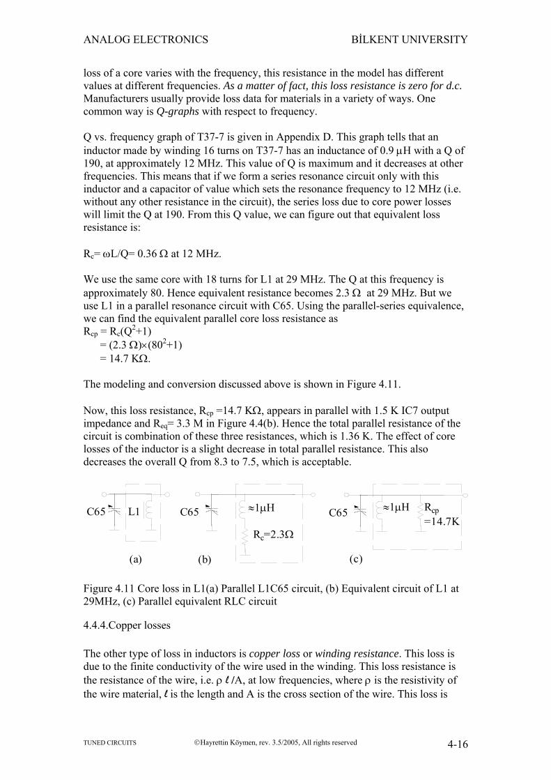
loss of a core varies with the frequency, this resistance in the model has different values at different frequencies. As a matter of fact, this loss resistance is zero for d.c. Manufacturers usually provide loss data for materials in a variety of ways. One common way is Q-graphs with respect to frequency. Q vs. frequency graph of T37-7 is given in Appendix D. This graph tells that an inductor made by winding 16 turns on T37-7 has an inductance of 0.9 µH with a Q of 190, at approximately 12 MHz. This value of Q is maximum and it decreases at other frequencies. This means that if we form a series resonance circuit only with this inductor and a capacitor of value which sets the resonance frequency to 12 MHz (i.e. without any other resistance in the circuit), the series loss due to core power losses will limit the Q at 190. From this Q value, we can figure out that equivalent loss resistance is: Rc= ωL/Q= 0.36 Ω at 12 MHz. We use the same core with 18 turns for L1 at 29 MHz. The Q at this frequency is approximately 80. Hence equivalent resistance becomes 2.3 Ω at 29 MHz. But we use L1 in a parallel resonance circuit with C65. Using the parallel-series equivalence, we can find the equivalent parallel core loss resistance as Rcp = Rc(Q2+1) = (2.3 Ω)×(802+1) = 14.7 KΩ. The modeling and conversion discussed above is shown in Figure 4.11. Now, this loss resistance, Rcp =14.7 KΩ, appears in parallel with 1.5 K IC7 output impedance and Req= 3.3 M in Figure 4.4(b). Hence the total parallel resistance of the circuit is combination of these three resistances, which is 1.36 K. The effect of core losses of the inductor is a slight decrease in total parallel resistance. This also decreases the overall Q from 8.3 to 7.5, which is acceptable.
(a)
C65 L1
(b)
C65 ≈1µH
Rc=2.3Ω
≈1µH
(c)
C65 Rcp=14.7K
Figure 4.11 Core loss in L1(a) Parallel L1C65 circuit, (b) Equivalent circuit of L1 at 29MHz, (c) Parallel equivalent RLC circuit
4.4.4.Copper losses The other type of loss in inductors is copper loss or winding resistance. This loss is due to the finite conductivity of the wire used in the winding. This loss resistance is the resistance of the wire, i.e. ρ l /A, at low frequencies, where ρ is the resistivity of the wire material, l is the length and A is the cross section of the wire. This loss is
further aggravated at RF because of a phenomenon called skin effect. As the frequency increases, the current is no longer homogeneously distributed across the cross section of the conductor, but it is confined to a thin cylindrical layer next to the conductor surface. Hence the cross section of the wire is effectively decreased, resulting in a larger winding resistance. The approximate cut-off frequency, above which skin effect becomes significant is given as, fsc ≈ 0.08/d 2 where fsc is frequency in MHz and d is the diameter of the wire in mm. The resistance of the wire, R, at a frequency f above fsc, is roughly R ≈ Rdc(f/fsc)1/2
where Rdc is the d.c. resistance of the wire. This corresponds to ten times increase in the resistance for an increase of two decades in frequency, above fsc. For example, a copper wire of 1 mm diameter has a d.c. resistance of 0.0215 Ω/m. If we use a length of 10 cm to make the winding, the total d.c. resistance becomes 0.1m×0.0215 Ω/m = 2.15E-3 Ω, or 2.15 mΩ. The fsc for this wire is 8E-2 MHz, or 80 KHz. Then, at 29 MHz, R becomes 41 mΩ. The winding resistance is also in series with the inductance, in inductor model. Hence it is possible to include one loss resistance to the model, to represent the sum of core and winding losses. It is common practice to choose sufficiently thick wires in inductors, to make the winding resistance negligible compared to inductance reactance and other losses.
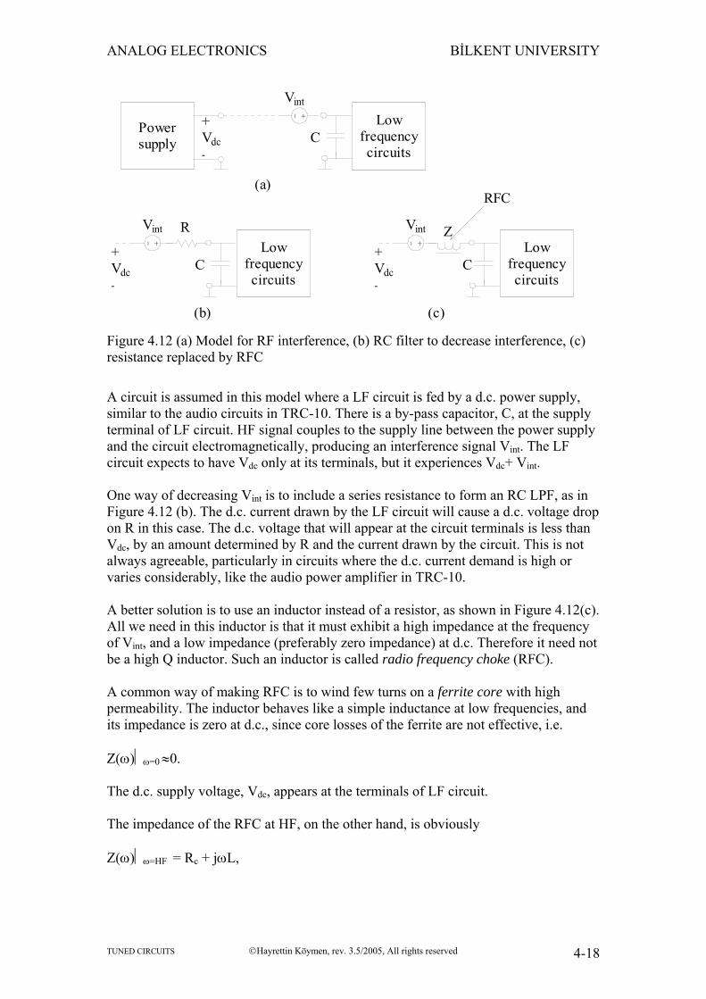
4.4.5. RF choke inductors While core loss degrades the performance of an inductor used in resonant circuits, it provides useful properties for wide band applications. A particularly important application area is the Electromagnetic Compatibility (EMC)/Electromagnetic Interference (EMI) engineering. The interference of RF signals within the same instrument or between instruments must be avoided in electronic circuits. Voltages or currents can couple to other parts of the circuits where they are not wanted, by electromagnetic means. Interference of irrelevant signal in a circuit can cause an instrument to malfunction. Studies related to keep this effect under control is called EMC/EMI. A typical RF interference to the power supply line is shown in Figure 4.12(a).
(c) Figure 4.12 (a) Model for RF interference, (b) RC filter to decrease interference, (c) resistance replaced by RFC
A circuit is assumed in this model where a LF circuit is fed by a d.c. power supply, similar to the audio circuits in TRC-10. There is a by-pass capacitor, C, at the supply terminal of LF circuit. HF signal couples to the supply line between the power supply and the circuit electromagnetically, producing an interference signal Vint. The LF circuit expects to have Vdc only at its terminals, but it experiences Vdc+ Vint. One way of decreasing Vint is to include a series resistance to form an RC LPF, as in Figure 4.12 (b). The d.c. current drawn by the LF circuit will cause a d.c. voltage drop on R in this case. The d.c. voltage that will appear at the circuit terminals is less than Vdc, by an amount determined by R and the current drawn by the circuit. This is not always agreeable, particularly in circuits where the d.c. current demand is high or varies considerably, like the audio power amplifier in TRC-10. A better solution is to use an inductor instead of a resistor, as shown in Figure 4.12(c). All we need in this inductor is that it must exhibit a high impedance at the frequency of Vint, and a low impedance (preferably zero impedance) at d.c. Therefore it need not be a high Q inductor. Such an inductor is called radio frequency choke (RFC). A common way of making RFC is to wind few turns on a ferrite core with high permeability. The inductor behaves like a simple inductance at low frequencies, and its impedance is zero at d.c., since core losses of the ferrite are not effective, i.e. Z(ω)ω=0 ≈0. The d.c. supply voltage, Vdc, appears at the terminals of LF circuit. The impedance of the RFC at HF, on the other hand, is obviously Z(ω)ω=HF = Rc + jωL,
where Rc is the core loss resistance. Hence having a large core loss is preferable for this application. The effect of Vint at circuit terminals is what is left after the voltage division between Z and C: Vint/(1– ω2LC+jωRcC). We use few RFCs in TRC-10. We use a hollow cylindrical core with a height of 5 mm, and with inner and outer diameters of 2 mm and 4 mm, respectively. Such cores are called beads. Neosid manufactures this particular bead, and the ferrite material is called F19. The specifications of this bead tells that a single turn on this core yields an impedance of Z= 27 Ω at 25 MHz. Indeed 18 turns yield an impedance of 8 K at 29 MHz and this impedance is predominantly resistive (i.e. Rc dominates over reactive part). Hence if we use this RFC with a by-pass capacitor of 10 nF, Vint is attenuated by 1/15000 (or by 83 dB) approximately, while Vdc is maintained intact. The voltage at the terminals of LF circuit becomes approximately Vdc+ Vint/15000.
4.5. RF Amplification using OPAMPs We employed OPAMPs for amplification of audio signals in Chapter 3. There we implicitly assumed that the open loop gain, A, of the OPAMP is constant for all frequencies. If we examine the “Open Loop Frequency Response” graph in the data sheet of TL082, where gain is plotted versus frequency, we observe that the gain is constant upto about only 20 Hz. Above this frequency gain falls at 20 dB/decade as the frequency increases.
4.5.1. OPAMP Open Loop Frequency Response As a matter of fact, OPAMP gain is not constant, but it is a complex function of frequency, called open loop frequency response, which can be expressed as Aol(ω) = A/(1+jω/ωo) where Aol is the open loop gain, A is the open loop gain at d.c. (i.e. 3.0E5, the value we used in Chapter 3), and ωo is the 3-dB frequency or break frequency where gain starts falling, 20 Hz for TL082. The assumption of constant gain for all frequencies did not cause any errors in the analysis of audio circuits, because audio circuits are processing signals at few KHz. At those audio frequencies, the data sheet shows that |Aol(ω)| is about 70 dB, or 3000. We used the TL082 in a feedback configuration to deliver gains of about 50, and the assumption of Aol(ω) → ∞ was acceptable. Should we try to use TL082 for amplifying signals at HF, we must first check the suitability of its frequency response. The same graph tells us that TL082 can provide a gain of 0 dB, or 1, at about 3 MHz. This means that it is not acting like an amplifier at HF.
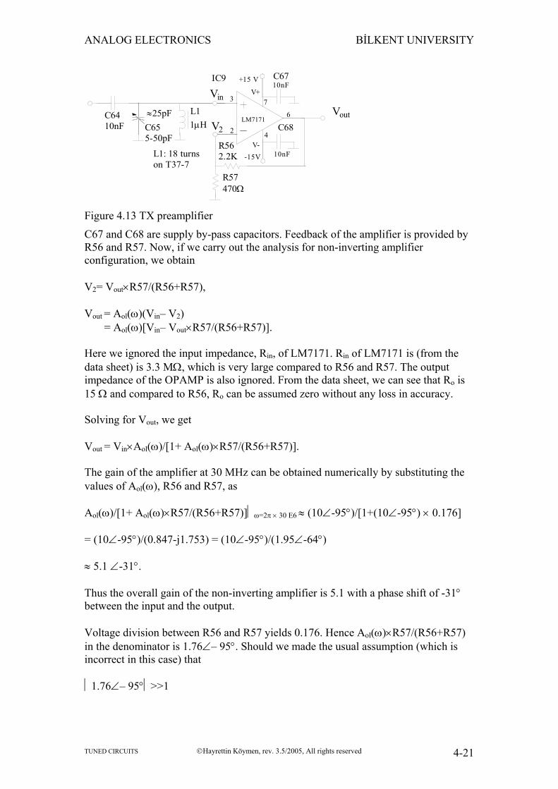
We use high frequency OPAMPs, like LM7171, for amplification at HF. The data sheet of LM7171 is given in Appendix A. We can see that A= 85 dB, |Aol(ω)| = 1 at about 200 MHz and |Aol(ω)| ≈ 20 dB, or 10, at 30 MHz. The open-loop phase shift between input and output is often reported in OPAMP data sheets indirectly as phase margin. Phase margin is an important concept related to stability considerations, discussion of which is left to more advanced texts. The open-loop phase shift information at any frequency can be obtained from the phase margin data by subtracting 180°. The phase margin at 30 MHz is approximately 85° and hence the open-loop phase shift between the input and output is –95°. This OPAMP is suitable for amplification at HF. A single break frequency can cause a phase shift up to 90°. Other capacitive effects in the IC become significant at higher frequencies in OPAMPs, as in the case of LM7171. This can be modeled by a second break frequency as Aol(ω) = A/[(1+jω/ωo1)×(1+jω/ωo2)]. Using the above data, we can express the open loop gain at 30 MHz as Aol(ω)ω=2π × 30 E6 = A/[(1+jω/ωo1)×(1+jω/ωo2)]ω=2π × 30 E6 ≈10∠-95°. We cannot see the first 3-dB frequency in the data sheet and therefore we cannot calculate the first break frequency. It is obvious that 30 MHz is much higher than the first break frequency, since the phase margin plot has reached a plateau long before frequency reaches 30 MHz. Mathematically this corresponds to (1+jω/ωo1) ≈ jω/ωo1. Therefore we can consider that the -90° of the phase shift is due to first break frequency and -5° is because of the second break frequency, i.e. Aol(ω)ω=2π×30E6 ≈ A/[(jω/ωo1)×(1+jω/ωo2)]ω=2π × 30 E6 ≈10∠-90°∠-5°. for LM7171. Hence the second break frequency, ωo2, can be found from ω/ωo2ω=2π × 30 E6 = tan(5°) as 2.16 E 9 rad/sec, or 343 MHz, approximately. Consider the TX preamplifier circuit of TRC-10, shown in Figure 4.13. This amplifier stage is a non-inverting amplifier and its input is the voltage developed across the parallel tuned circuit of C65 and L1.
C67 and C68 are supply by-pass capacitors. Feedback of the amplifier is provided by R56 and R57. Now, if we carry out the analysis for non-inverting amplifier configuration, we obtain V2= Vout×R57/(R56+R57), Vout = Aol(ω)(Vin– V2) = Aol(ω)[Vin– Vout×R57/(R56+R57)]. Here we ignored the input impedance, Rin, of LM7171. Rin of LM7171 is (from the data sheet) is 3.3 MΩ, which is very large compared to R56 and R57. The output impedance of the OPAMP is also ignored. From the data sheet, we can see that Ro is 15 Ω and compared to R56, Ro can be assumed zero without any loss in accuracy. Solving for Vout, we get Vout = Vin×Aol(ω)/[1+ Aol(ω)×R57/(R56+R57)]. The gain of the amplifier at 30 MHz can be obtained numerically by substituting the values of Aol(ω), R56 and R57, as Aol(ω)/[1+ Aol(ω)×R57/(R56+R57)]ω=2π × 30 E6 ≈ (10∠-95°)/[1+(10∠-95°) × 0.176] = (10∠-95°)/(0.847-j1.753) = (10∠-95°)/(1.95∠-64°) ≈ 5.1 ∠-31°. Thus the overall gain of the non-inverting amplifier is 5.1 with a phase shift of -31° between the input and the output. Voltage division between R56 and R57 yields 0.176. Hence Aol(ω)×R57/(R56+R57) in the denominator is 1.76∠– 95°. Should we made the usual assumption (which is incorrect in this case) that 1.76∠– 95°>>1
in the gain expression, we could ignore the effect of “1” in [1+Aol(ω)×R57/(R56+R57)] and obtain the gain approximately as 1+R56/R57≈5.7, without any phase shift. Note that even with an open loop gain as low as 10, the gain we obtain is reasonably close to the gain obtained with ideal OPAMP assumption.
4.5.2. Voltage gain and power gain We calculated that the voltage gain of TX preamplifier stage as 5.1, or 14.2 dB. The power gain of this stage can also be calculated. Referring to Figure 4.4(b), the input voltage and power delivered to this stage are Vin= I(1.5K) and Pin= ½ I2(1.5K), respectively, where 1.5 K is the output resistance of the mixer chip IC7. Since the gain of the amplifier is 5.1, Vout is (5.1)× I(1.5K). Referring to Figure 4.8(b), the load connected to the output of the amplifier at resonance, 30 MHz, is 100 Ω. The power delivered to the load is the current through the load resistor times the voltage across it, Pout = ½ [(Vout)/(Ro+100Ω)][(Vout)×(100 Ω)/(Ro+100Ω)] = ½ Vout
2[100/(15+100)2]. Substituting the value of Vout, we obtain Pout = ½ [(5.1)× I(1.5K)]2[7.56E-3]. Hence the power gain is Pout/Pin= (5.1)2×(1.5K)×(7.56E-3) = 295, or 24.7 dB. The power gain is considerably larger compared to the voltage gain. This is because of the fact that, when the amplifier processes the signal, it is not only amplified, but the impedance that the signal appears across, decreases from 1.5 K to 100 Ω. There is an impedance transformation. As a result of this impedance transformation, we obtain a power gain, which is 10.5 dB larger than the voltage gain.
4.5.3. Slew Rate As far as the signal amplitudes are small, open loop transfer function is the limiting factor for output voltage amplitude. When the signal amplitudes become larger, another limitation due to slew rate of the OPAMP emerges. Slew rate is the maximum slope of the output voltage that can be amplified by the OPAMP without any distortion. Assume that the signal is a sinusoidal voltage v(t)=Vpcosωt. Then the maximum slope of this signal is dv(t)/dtmax= Vpω.
The product Vpω must not exceed the slew rate limit of the OPAMP in order to have amplification without any distortion. We can see in the data sheet that LM7171 has a very high slew rate of 4100V/µs at unity gain. This means that, for example at 30 MHz, Vp < 4100 (V/µs)/(2π×30E6 rad/sec) = 21.75 V, which is significantly larger than our requirement (notice that the supply voltage is ±15 V, and hence output voltage amplitude, Vp, must be less than 15 V anyway).
4.5.4. Input Bias Current In order that an OPAMP can operate, it draws certain amount of d.c. current into its input pins from the external circuits. This current is called input bias current. The magnitude of this current is usually small, but must be carefully taken care of in every application. Circuits connected to both positive and negative input pins (i.e. pins 3 and 2 respectively in case of LM7171) must allow a d.c. current path to a supply or to ground, so that this bias current can flow and OPAMP can work. For example there must not be a series capacitor, blocking all the d.c. current. In the TX preamplifier in Figure 4.13, d.c. path for pin 3 is provided by the inductance L1 and for pin 2, by R56 and R57. Input bias current of LM7171 is given as 12 µA maximum (IB in the data sheet). TL082 is an “FET input OPAMP” and has a very low input bias current of 50 pA.
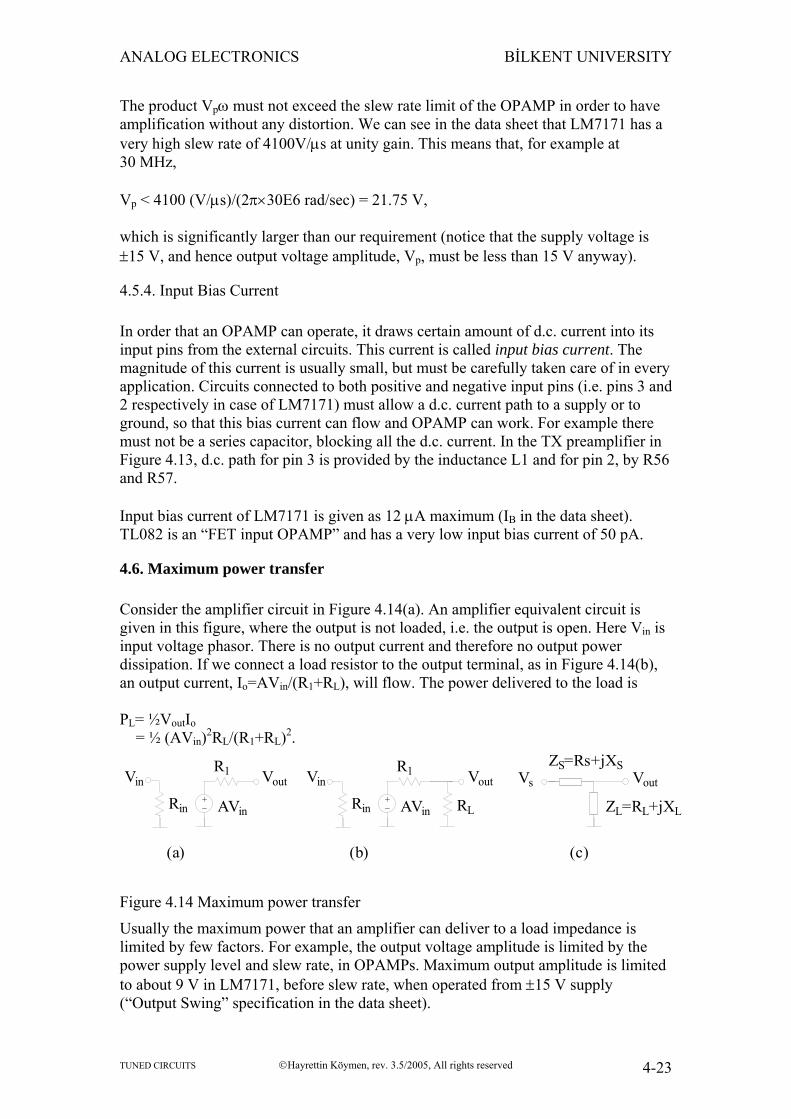
4.6. Maximum power transfer Consider the amplifier circuit in Figure 4.14(a). An amplifier equivalent circuit is given in this figure, where the output is not loaded, i.e. the output is open. Here Vin is input voltage phasor. There is no output current and therefore no output power dissipation. If we connect a load resistor to the output terminal, as in Figure 4.14(b), an output current, Io=AVin/(R1+RL), will flow. The power delivered to the load is PL= ½VoutIo = ½ (AVin)2RL/(R1+RL)2.
Rin
Vin Vout+_ AVin
R1
(b)
RLRin
Vin Vout+_ AVin
R1
(a)
Vs Vout
(c)
ZS=Rs+jXS
ZL=RL+jXL
Figure 4.14 Maximum power transfer
Usually the maximum power that an amplifier can deliver to a load impedance is limited by few factors. For example, the output voltage amplitude is limited by the power supply level and slew rate, in OPAMPs. Maximum output amplitude is limited to about 9 V in LM7171, before slew rate, when operated from ±15 V supply (“Output Swing” specification in the data sheet).
On the other hand, maximum output current is also limited in OPAMPs. For example, maximum output current amplitude is limited to about 90 mA in LM7171. Hence, the maximum power we can get from an amplifier using LM7171 is 0.4 W at best. If we further examine the data sheet, for example from undistorted output point of view, other limitations decrease this maximum power level to a significantly lower one at high frequencies. Thus, the available output power is limited. Occasionally we find ourselves in a situation where we wish to deliver as much power as possible to the load. If we carefully examine the expression for PL above, we can see that ½ (AVin)2 RL/(R1+RL) is the limited available power and we can only maximize PL by good choice of resistances. To find the value of RL, which yields maximum PL, we differentiate the expression for PL with respect to RL and equate it to zero: dPL/dRL= 0 ⇒ RL= R1. Hence load resistance must be equal to source resistance for maximum power transfer to the load. Both source and load impedances can be complex. This case is depicted in Figure 4.14(c). The complex power delivered to the load in this case is PL=½ [Vs ZL/(ZS+ZL)]Is
*, Where Is is the current flowing through ZL. Substituting Is
* =[Vs/(ZS+ZL)]*
we obtain PL=½ (Vs Vs
*) ZL/|ZS+ZL|2. The complex power PL has two components. The real part is the average power and it is dissipated on RL. The imaginary part is the reactive power and it is not dissipated. This component is the power that goes to the capacitors and/or inductors. However the reactive power must be available to the circuit in order that the circuit can function. There is no point to maximize the reactive part since this component is only temporarily borrowed by ZL. The component to be maximized is the real part. The real power delivered to the load is the average power PLa= Re[PL] = ½ (Vs)2 RL/[(RL+RS)2+( XL+XS)2]. First of all it is clear that XL and XS must sum up to zero to maximize PL, i.e. XL= -XS. With this condition imposed, the rest of the expression reduces to the all-resistive case, which yields RL=RS for maximum PL. Hence the general form of maximum power transfer condition is ZL=ZS
In other words, load impedance must be equal to the complex conjugate of the source impedance for maximum power transfer to load. The maximum power that can be delivered to load by a source, which is also called available power, is PL= PA= Vs
2/8RS where Vin is the source voltage amplitude and RS is the real part of source impedance.
4.7. Bibliography The ARRL Handbook has a very good chapter on real world components (Chapter 10). Following web sites provide a wealth of information on various core materials and their applications: www.ferroxcube.comwww.micrometals.comwww.neosidcanada.comhttp://bytemark.com/amidon Op-amps and Linear Integrated Circuits by R.A.Gayakwad has a good chapter on OPAMP frequency response.
4.8. Laboratory Exercises 1. Read all Laboratory Exercises of this chapter carefully.
Radio amplifiers 2. The first RF circuit to be mounted is the TX preamplifier and the tank circuit at its
input. This sub-circuit is given in Figure 4.13. We analyzed all parts of this circuit in the chapter. Cut a 30 cm long piece of 0.5 mm thick enameled wire. Carefully wind 18 turns on a T37-7 toroid, to make 1 µH inductor L1. Count the turns carefully. It is very easy to end up by one turn more. Number of turns is the number of times the wire passes through the toroid. Spread the turns evenly around the toroid, otherwise the inductance will be significantly larger than the calculated value. Trim the wires to leave about 1 cm length at each lead for connection. Strip the enamel at each end for about 3 mm length, using your pocket knife or sand paper. Burning the enamel coating with a lighter before using sand paper or pocketknife helps. Stripping the enamel fully is very important. If you do not strip it properly, you will have a bad solder connection and your circuit will work and stop intermittently. It may be very annoying and time consuming to correct this later. Coat the stripped part with a thin layer of solder. If the enamel is not stripped fully, solder will not cover the wire smoothly but beads of solder will form on the wire. L1 is now ready. Install and solder L1 on the PCB. Tie it on the PCB using a plastic strip. C65 is a trimmer capacitor and has three pins. One pin is connected to the trimming screw. That pin must be connected to the ground. Install C65 and solder it. The tank circuit is now ready. Install and solder the supply by-pass capacitors C67 and C68.
Install the feedback resistors R56 and R57. Leave the resistors few mm above the board so that you can connect the oscilloscope probes. Solder the resistors. Install one lead of the by-pass capacitor C64 to the hole on the C65 side only and solder it. Leave the lead on the IC7 side on the surface of PCB, for measurements. Examine the data sheet of LM7171 for pin configuration and soldering information. Install IC9 carefully. Make sure that the mark on the IC fits to the one on PCB. Check if all pins are at their proper positions. Solder all the pins carefully. Check all connections using a multimeter for connectivity and for short circuits. TX preamplifier is now ready for testing and tuning.
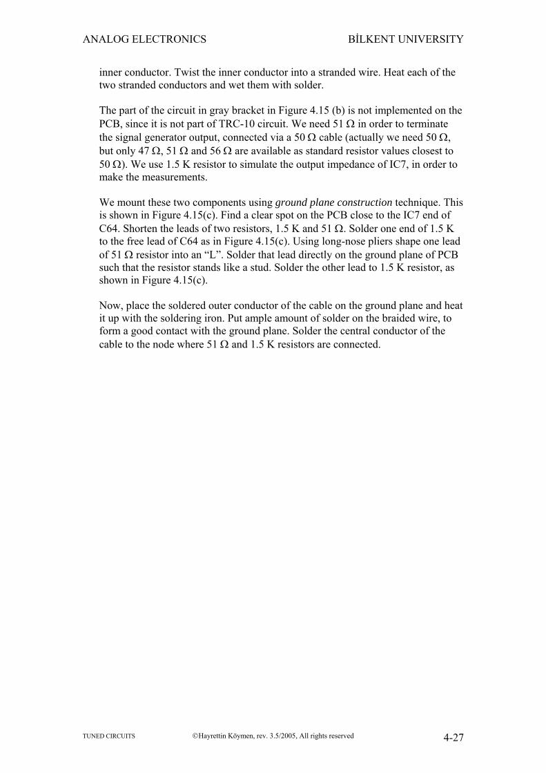
3. Ordinary pair of cables are not suitable to make connections of length more than few tens of centimeters at HF. We already discussed that there is always an inductance associated with a length of wire and a capacitance between two wires. These parasitic elements become significant as the frequency of interest increases, particularly if the wires are long. We use special cables in which this inductance and capacitance are carefully controlled. Coaxial cables are such cables. Cables of all oscilloscope probes, for example, are coaxial cables. RG58/U is a common laboratory grade coaxial cable, which is composed of a central conductor wire and an outer conductor. Outer conductor is a cylindrical braided wire, concentric with the central conductor. In between, there is a solid but flexible insulator, made of an insulating plastic material, which maintains the concentricity. The outermost layer is an insulating plastic sheath.
The ratio of incremental inductance (L) and capacitance (C) along the cable is maintained constant in coaxial cables. In RG58/U, (L/C)1/2 is 50 Ω. (L/C)1/2 is called the characteristic impedance of the cable. Hence, RG58/U is a 50 Ω coaxial cable. Usually BNC type connectors are used with RG58/U. These are bayonet type twist-and-fit connectors. Signal generators are not ideal voltage sources with zero output impedance, but have finite output impedance. Most widely used standard is 50 Ω. The output levels of a signal generator are specified assuming that there is a 50 Ω termination (load) impedance connected to its output. If a cable connects a 50 Ω load to the generator, it is required that the characteristic impedance of the cable must also be 50 Ω for proper operation at high frequencies. Figure 4.15(a) shows how we must connect the signal generator, oscilloscope and the circuit to make the measurements. Figure 4.15(b) shows how the coaxial cable from the signal generator must be connected to the circuit and the oscilloscope probe connection. To connect the signal generator to the circuit, we shall use a very reliable laboratory measurement technique. We use a coaxial cable of about 1 m length, with a BNC connector on one end. Remove the black insulating sheath for about 1.5-2 cm from the bare end using your pocketknife, without damaging the braided outer conductor. Undo the exposed braid and twist it into a thick stranded wire. Remove about 5 mm of the inner polyethylene insulator without damaging the
inner conductor. Twist the inner conductor into a stranded wire. Heat each of the two stranded conductors and wet them with solder. The part of the circuit in gray bracket in Figure 4.15 (b) is not implemented on the PCB, since it is not part of TRC-10 circuit. We need 51 Ω in order to terminate the signal generator output, connected via a 50 Ω cable (actually we need 50 Ω, but only 47 Ω, 51 Ω and 56 Ω are available as standard resistor values closest to 50 Ω). We use 1.5 K resistor to simulate the output impedance of IC7, in order to make the measurements. We mount these two components using ground plane construction technique. This is shown in Figure 4.15(c). Find a clear spot on the PCB close to the IC7 end of C64. Shorten the leads of two resistors, 1.5 K and 51 Ω. Solder one end of 1.5 K to the free lead of C64 as in Figure 4.15(c). Using long-nose pliers shape one lead of 51 Ω resistor into an “L”. Solder that lead directly on the ground plane of PCB such that the resistor stands like a stud. Solder the other lead to 1.5 K resistor, as shown in Figure 4.15(c). Now, place the soldered outer conductor of the cable on the ground plane and heat it up with the soldering iron. Put ample amount of solder on the braided wire, to form a good contact with the ground plane. Solder the central conductor of the cable to the node where 51 Ω and 1.5 K resistors are connected.
Oscilloscope channel 2 probeconnected to this point
RG58/Ucoaxial cable
100Ω
(b)
(c)
RG58/Ucoaxial cable
51Ω
1.5 K
C64
strandedcentralconductor
polyethyleneinsulation
tinned copperbraid
(a)
Oscilloscope
28.85
Signal generator
RG58/U Coax
Probe
PCB
Figure 4.15 (a) Measurement set up for TX preamplifier, (b) circuit and connections on PCB, (c) ground-plane construction of test circuit components
Vout node must be terminated by a 100 Ω resistor also, as in the actual circuit. Install and solder one lead of R58 to the hole connected to Vout. Solder the other lead directly on the ground plane, for the time being. Make sure all soldered joints are very good joints.
ANALOG ELECTRONICS BİLKENT UNIVERSITY
Ground plane construction technique provides an excellent trial and measurement environment. Parasitic effects are minimum in this circuit construction technique.
4. Before connecting the signal generator and the oscilloscope, switch the power ON, and check the circuit for d.c. voltages. Using a multimeter, measure the supply voltages at the OPAMP terminals, and make sure that they read ±15 V. Vout must be within few mV of zero, and the voltages at pins 2 and 3 must read zero. Switch the power OFF. Switch the signal generator ON and set the signal to CW (continuous wave) sinusoid at the frequency of 28.85 MHz. Set the amplitude to 100 mV (rms), or –7 dBm (recall that -7 dBm is 0.2 mW, the power delivered to 50 Ω resistor when 100 mV is applied across it). Switch the oscilloscope ON. Set the first channel to 0.1 V/div vertical and 50 nsec/div horizontal resolution. Trigger the oscilloscope and stabilize the waveform on the scope. Switch the power of the circuit ON. Connect the oscilloscope (channel 2) probe to the output of the OPAMP, by hooking it to the corresponding pin of R58. Set the vertical axis to 0.2 V/div. Using alignment tool, adjust C65 such that the amplitude of Vout is made maximum. Measure the amplitude and record it. Congratulations! You had just tuned your tank circuit.
Calculate the absolute value of the voltage gain, and in dB, at 28.85 MHz. The output is what you observe on channel 2 and input is on channel 1. Calculate the power delivered to 100 Ω resistor. Note that we base our calculations to the measurement made at the output of the amplifier only, rather than making another measurement directly across the tuned circuit. Making a direct measurement on the tuned circuit is not straightforward. Recall the Lab Exercise 3 of Chapter 3. Even when the probe is carefully compensated, Cp, the capacitance at the tip of the probe, appears directly across the circuit the probe is connected to (see problem 23). Although Cp, is a small capacitance in the order of 10 pF, it may load the circuits which has low parallel capacitance, at high frequencies. In this tuned circuit the parallel capacitance is only few tens of pF and a probe connection will definitely off-tune it. Special low-capacitance “FET probes” are used at higher frequencies.
5. The gain you have obtained experimentally may be less than 5.1, as calculated in Section 4.5.1. This is because of two reasons: 1. Open Loop Gain of an OPAMP is usually reported for the case when the
OPAMP is unloaded, or loaded by a large resistor. When the load impedance is small, the current demand from the amplifier increases and there can be a decrease in the gain. In TX preamplifier circuit, the load resistor is 100 Ω. In the data sheet, this variation of the gain with respect to load resistance is given for large signal case. Large signal case means that the amplitude of the signal at the output is close to the limits of the OPAMP. Signal levels at the output of TX preamplifier in the previous exercise can be considered as small signal. Hence there is not any data that we can use directly. However, we can deduce
from the large signal data that the nominal open loop gain can be 4 dB less than the nominal gain reported for 1 K load resistance. This corresponds to having a gain of 16 dB instead of 20 dB at 30 MHz.
2. There may be a difference in the open loop gain of OPAMPs coming from different production batches.
Calculate the voltage and power gain of the TX preamplifier stage if the open loop gain of the OPAMP is 16 dB with a phase margin of 80°, following the calculation method given in Section 4.5.1. Is the difference of 10.5 dB between the power gain and voltage gain is maintained, although the voltage gain decreased?
6. We shall now measure the transfer response of this stage using the set up in Exercise 3. Measure the output voltage amplitude at about 20 different frequencies between 1 MHz and 30 MHz (40 MHz if the signal generator allows), while keeping the input signal at –7 dBm. Choose the frequencies cleverly in order to characterize both the pass band of the tank circuit around 29 MHz and its suppression at around 3 MHz. Calculate the voltage gain in dB and plot it versus frequency on a graph paper with a linear scaled vertical axis and logarithmic scaled horizontal axis.
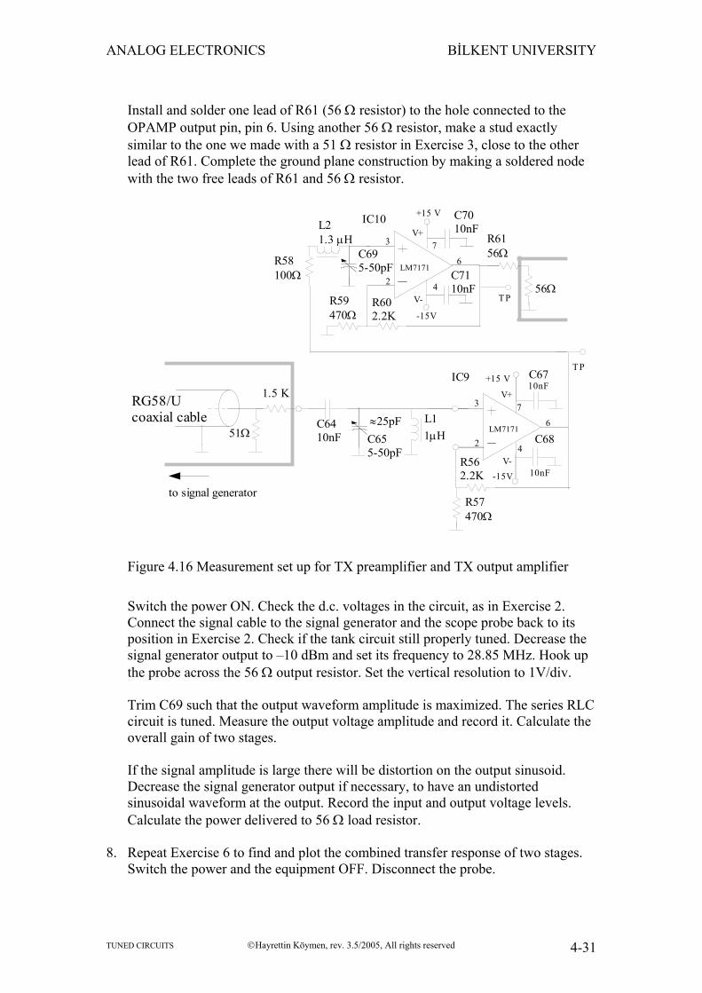
7. Although the voltage gain we obtained in preamplifier stage may not be impressive, we obtained a good power gain and we filtered the transmit signal to some extent. We shall now increase this power level more by first increasing the voltage level using a series RLC circuit and then another OPAMP, in TX output amplifier. L2 is a 1.3 µH inductor. We shall make this inductor by winding 20 turns on T37-7 toroid. Use a 30 cm length of 0.2 mm diameter enamel coated wire and make the inductor carefully, following the procedure described for L1. The circuit diagram of TX output amplifier is given in Figure 4.16. Make sure that the power of the circuit is switched OFF. Disconnect the probe from the circuit and coaxial signal cable from the signal generator, so that none of the equipment has any connection to the circuit. De-solder the lead of R58 which was connected to ground plane. Using de-soldering pump, remove the remaining solder on the ground plane. Install that lead of R58 to its proper hole and solder. Install and solder L2 and C69. Take care to place C69 such that its trimmer lead is connected to ground. Install and solder the OPAMP IC10, by-pass capacitors C70, C71, C54 and C55, and the feedback resistors R59 and R60. C54 and C55 have polarity and be careful to place them correctly before soldering. Also, be careful while installing LM7171 to place it correctly on the PCB. This amplifier drives the output circuit, which is connected to the antenna. Antennas are designed usually to have a standard input impedance like 50 Ω, 75 Ω, etc. The output stage of TRC-10 is designed to drive an antenna with input impedance of 50 Ω. We simulate this impedance when testing the output amplifier, by using an extra 56 Ω resistor and ground plane construction, as shown in the gray bracket in at the output.
Install and solder one lead of R61 (56 Ω resistor) to the hole connected to the OPAMP output pin, pin 6. Using another 56 Ω resistor, make a stud exactly similar to the one we made with a 51 Ω resistor in Exercise 3, close to the other lead of R61. Complete the ground plane construction by making a soldered node with the two free leads of R61 and 56 Ω resistor.
51Ω
1.5 K
to signal generatorR57470Ω
1µHC6410nF
≈25pFLM7171
3
2
6
7
4
V+
V-10nF
10nF+15 V
-15V
C655-50pF
IC9
L1
C67
C68
R562.2K
RG58/Ucoaxial cable
56Ω
+15 V
-15V
L21.3 µH
R58100Ω
R6156Ω
T P
T P
IC10
C695-50pF C71
10nFR59470Ω
R602.2K
LM7171
3
2
6
7
4
V+
V-
C7010nF
Figure 4.16 Measurement set up for TX preamplifier and TX output amplifier
Switch the power ON. Check the d.c. voltages in the circuit, as in Exercise 2. Connect the signal cable to the signal generator and the scope probe back to its position in Exercise 2. Check if the tank circuit still properly tuned. Decrease the signal generator output to –10 dBm and set its frequency to 28.85 MHz. Hook up the probe across the 56 Ω output resistor. Set the vertical resolution to 1V/div. Trim C69 such that the output waveform amplitude is maximized. The series RLC circuit is tuned. Measure the output voltage amplitude and record it. Calculate the overall gain of two stages. If the signal amplitude is large there will be distortion on the output sinusoid. Decrease the signal generator output if necessary, to have an undistorted sinusoidal waveform at the output. Record the input and output voltage levels. Calculate the power delivered to 56 Ω load resistor.
8. Repeat Exercise 6 to find and plot the combined transfer response of two stages. Switch the power and the equipment OFF. Disconnect the probe.
9. We shall measure the amount of distortion on the output waveform using a spectrum analyzer. Spectrum analyzer is an instrument, which measures and plots the frequency components of a signal with respect to frequency. The frequency components are measured in terms of power (dBm) delivered to 50 Ω input impedance of the analyzer. TX output amplifier is expected to deliver about 40 mW to the antenna, at 29 MHz. Although the amplifier is a linear amplifier, there is distortion on the RF signal when the OPAMP is driven at its limits. Distortion means that there are signal components clustered around harmonics of 29 MHz. Signals produced by transmitters at frequencies other than the transmission frequency are called spurious emissions (like harmonics of the carrier), which must be suppressed. The TX amplifier is a linear amplifier and the carrier waveform at the output is predominantly sinusoidal. The data sheets of LM7171 reveal that we must be able to get an output signal with about 3% distortion at full power. Spectrum analyzers usually have 50 Ω input impedance and can handle a maximum of 0 dBm input power. We must attenuate the TX output by more than 10 dB before connecting to the analyzer. We use the set up in Figure 4.16 with 56Ω termination resistance replaced by a three resistor attenuator and connection to spectrum analyzer, as shown in Figure 4.17. The circuit enclosed in gray bracket must be mounted using ground plane construction technique. The 10 nF capacitor is a d.c. decoupling capacitor. It blocks the d.c. path between the IC10 output and the spectrum analyzer. The circuit in the shaded box is the attenuator. It attenuates the IC10 output delivered to 56 Ω load in Figure 4.16, Vo1, before it is presented to the spectrum analyzer as Vo2, while it maintains approximately 50 Ω termination at both ends. Calculate the output impedance of the attenuator Zo, assuming that the output impedance of IC10 is zero and 10 nF capacitor is virtually short circuit above 28 MHz. Calculate the attenuation from Vo1 to Vo2 in dB, considering the impedance across the coaxial cable is the input impedance of the spectrum analyzer, 50 Ω. What is the maximum signal power that IC10 can deliver to the analyzer now?
Zo Figure 4.17 Measurement set up in Figure 4.16 modified for harmonic measurement
10. De-solder and remove 56 Ω termination resistor at the output in Figure 4.16.
Remove excess solder on the PCB, using de-soldering pump. Construct part of the circuit in gray bracket in Figure 4.17, comprising 10 nF capacitor, two 47 Ω resistors and 3.3 Ω resistor. The coaxial cable to the spectrum analyzer is actually a short cable terminated by the BNC antenna jack. We mount this jack on the back panel and the cable from the antenna is connected to it. We use this jack to make harmonic measurements in this exercise. A neat and geometrically correct connection of BNC jack to RG58/U is very important. Ask the lab technician to show you a correctly connected jack. Cut a 25 cm long RG58/U cable. Strip the plastic cover at both ends for about 1 cm. Strip the polyethylene insulation from the ends for about 3 mm. Twist the central conductor and put a solder cover on it. First fit the central conductor to its place on the jack and make a very neat solder connection. Then fit and solder the braid. Mount the antenna BNC jack to its place at the back panel tightly, with the nut provided. Prepare the free end of the coaxial cable for ground plane construction and connect it to the attenuator output, as we had done in Exercise 3. Check your connections.
11. Connect the cable with BNC plugs at both ends between the antenna jack and the spectrum analyzer. Ask the assistant or the lab technician to help you with the spectrum measurements. Switch the power on.
12. Set the signal generator frequency to 28.85 MHz and its voltage to the level you
recorded in Exercise 7. Measure the fundamental component and second and third harmonic power of the output signal. Correct these values using the attenuation you had calculated, and record them. Compare the fundamental component power to the one calculated in Exercise 7.
13. Disconnect the spectrum analyzer and the signal generator. Disconnect the coaxial cable to the spectrum analyzer. De-solder the other end of antenna jack cable form the PCB. You need the rest of the set up for harmonic measurements after the harmonic filter is installed. This measurement is the first experimental exercise in Chapter 5.
4.9. Problems 1. In a series RLC circuit, R= 100 Ω, L= 10 µH and C = 3 pF. Plot the magnitude
and the phase of the impedance as a function of ω for 0.6ωo<ω<1.5ωo.
2. A voltage 10∠0° is applied to the series circuit of Problem 1. Find the voltage across each element for f = 28, 29 and 29.7 MHz.
3. A series circuit with R = 50 Ω, C = 39 pF and variable inductor L has an applied
voltage V=10∠0° with a frequency of 16 MHz. L is adjusted until the voltage across the resistor is maximum. Find the voltage across each element.
4. A series circuit has R= 50 Ω, L = 1 µH and variable capacitor C. Find C for series
resonance at f = 16 MHz. 5. Given a series RLC circuit with R= 10 Ω, L = 0.5 µH and C = 220 pF, calculate
the resonant, lower and upper half power frequencies. 6. Show that the resonant frequency ωo of an RLC series circuit is the geometric
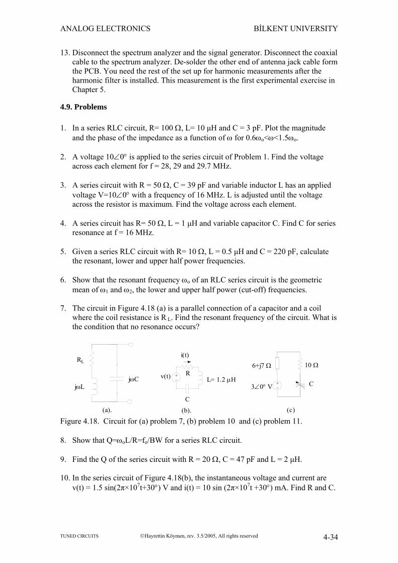
mean of ω1 and ω2, the lower and upper half power (cut-off) frequencies. 7. The circuit in Figure 4.18 (a) is a parallel connection of a capacitor and a coil
where the coil resistance is R L. Find the resonant frequency of the circuit. What is the condition that no resonance occurs?
RL
jωLjωC
(a).
+_v(t)
i(t)
RL= 1.2 µH
C
+_3∠0° V
6+j7 Ω 10 Ω
C
(c)(b). Figure 4.18. Circuit for (a) problem 7, (b) problem 10 and (c) problem 11. 8. Show that Q=ωoL/R=fo/BW for a series RLC circuit. 9. Find the Q of the series circuit with R = 20 Ω, C = 47 pF and L = 2 µH. 10. In the series circuit of Figure 4.18(b), the instantaneous voltage and current are
v(t) = 1.5 sin(2π×107t+30°) V and i(t) = 10 sin (2π×107t +30°) mA. Find R and C.
11. In the series circuit of Figure 4.18(c), the impedance of the source is 6+j7 and the source frequency is 10 MHz. At what value of C will the power in 10 Ω resistor be a maximum? What is this maximum power deliverable to 10 Ω resistor.
12. In the parallel circuit of Figure 4.19(a), determine the resonant frequency if R =
0Ω and R = 1Ω. Compare them to resonant frequency when R = 100 Ω.
13. In the parallel circuit in Figure 4.19(b) find the resonant frequency fo.
1 µH100 pF
R
(a)
540 nH2.2 nF
15 Ω
(b) Figure 4.19. Circuit for (a) problem 12 and (b) problem 13
14. Refer to Figures 1.11 and 1.13. There is a lower sideband signal component at
fIF - fVFO, at the output of TX Mixer. Calculate the approximate value of the attenuation this signal experiences compared to the upper side band component, after it is filtered by parallel RLC circuit of Figure 4.4.
15. Calculate the branch voltages, i.e. voltages across R58, L2 and C69, of the series
RLC circuit in Figure 4.8 if Vs = V∠0, at the resonance frequency. Write down the time waveform expressions for these voltages.
16. Calculate the same branch voltages in Exercise 15, at upper and lower 3-dB
frequency of the series circuit. Write down the time waveform expressions for these voltages.
17. Calculate the d.c. resistance of a 0.2 mm diameter wire of length 10cm. Calculate
its skin effect cut-off frequency. Calculate the approximate copper loss of an inductor made of this wire at 29 MHz.
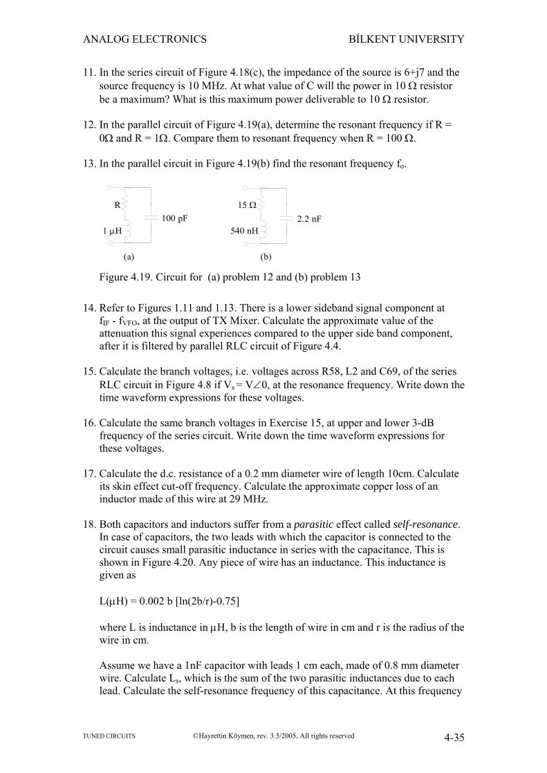
18. Both capacitors and inductors suffer from a parasitic effect called self-resonance.
In case of capacitors, the two leads with which the capacitor is connected to the circuit causes small parasitic inductance in series with the capacitance. This is shown in Figure 4.20. Any piece of wire has an inductance. This inductance is given as L(µH) = 0.002 b [ln(2b/r)-0.75] where L is inductance in µH, b is the length of wire in cm and r is the radius of the wire in cm. Assume we have a 1nF capacitor with leads 1 cm each, made of 0.8 mm diameter wire. Calculate Ls, which is the sum of the two parasitic inductances due to each lead. Calculate the self-resonance frequency of this capacitance. At this frequency
the capacitor appears like a short circuit. As the frequency is further increased, the capacitor exhibits an inductive reactance! The full equivalent circuit of a capacitance is given in Figure 4.20(c), for the sake of completeness. The parallel resistance Rp models the loss in the dielectric material from which the capacitor is made off, and series resistor Rs represents the sum of copper loss in the leads and the losses at the lead contacts. Usually Rp is very high and Rs is very low, and both of them can be ignored. The main parasitic effect is the self-resonance.
b
1n0capacitor
parasiticinductance
C
Ls
(a) (b)
C
Ls
Rp
Rs
(c)
Figure 4.20 (a) Capacitor, (b) Capacitor model with parasitic inductance, (c) Full high frequency model
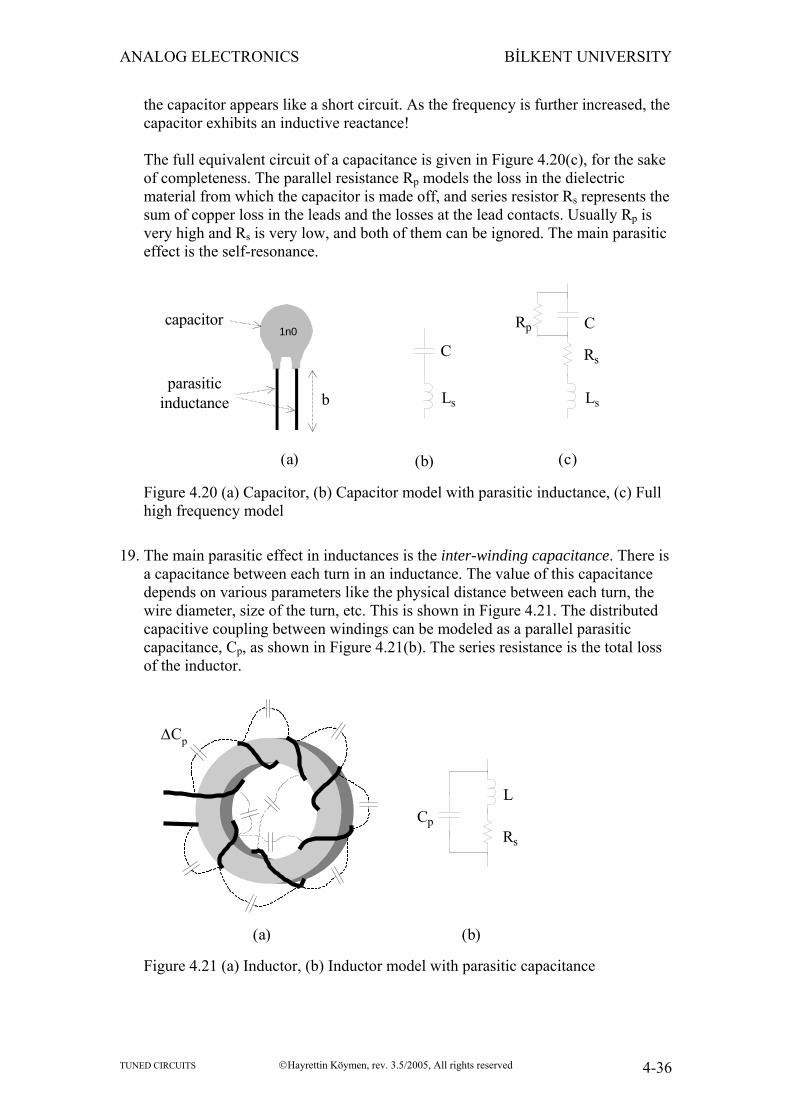
19. The main parasitic effect in inductances is the inter-winding capacitance. There is
a capacitance between each turn in an inductance. The value of this capacitance depends on various parameters like the physical distance between each turn, the wire diameter, size of the turn, etc. This is shown in Figure 4.21. The distributed capacitive coupling between windings can be modeled as a parallel parasitic capacitance, Cp, as shown in Figure 4.21(b). The series resistance is the total loss of the inductor.
(a) (b)
Cp
L
Rs
∆Cp
Figure 4.21 (a) Inductor, (b) Inductor model with parasitic capacitance
Cp is a small capacitance, usually less than a pF, but it can be effective in the frequencies of interest, particularly if the inductance value is large. An inductor made by winding 32 turns on a core, which has AL of 20 nH/turn2. the inductance is measured to be 20 µH at 1 MHz. The impedance of the inductor is purely resistive at 40 MHz. Assuming that the Q of the inductor is larger than 10 and AL is constant up to this frequency (which is not a good assumption since the permeability of most materials fall with increasing frequency), calculate the winding capacitance.
20. What must be the length of a 900 nH air core inductor if it has 21 turns and its
diameter is 5 mm?
21. AL of the T25-10 toroidal core is given as 1.9 nH/N2, where N is number of turns. Find the number of turns required to make a 615 nH inductor using T25-10.
22. An inductor made by winding 7 turns on T20-7 toroid yields 0.13 µH with a Q of 102 at 30 MHz. Find the approximate value of AL for T20-7 and the equivalent series core loss resistance of this inductor at 30 MHz.
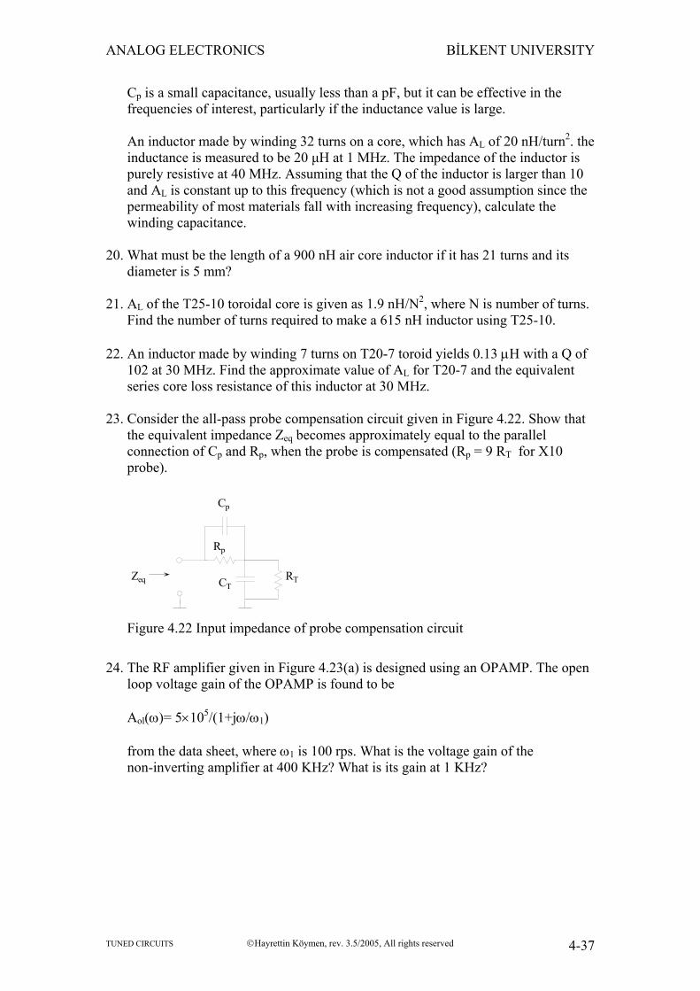
23. Consider the all-pass probe compensation circuit given in Figure 4.22. Show that
the equivalent impedance Zeq becomes approximately equal to the parallel connection of Cp and Rp, when the probe is compensated (Rp = 9 RT for X10 probe).
Cp
Rp
RTCTZeq
Figure 4.22 Input impedance of probe compensation circuit
24. The RF amplifier given in Figure 4.23(a) is designed using an OPAMP. The open
loop voltage gain of the OPAMP is found to be Aol(ω)= 5×10⁵/(1+jω/ω1) from the data sheet, where ω1 is 100 rps. What is the voltage gain of the non-inverting amplifier at 400 KHz? What is its gain at 1 KHz?
(b) Figure 4.23. Circuit for (a) problem 24 and (b) problem 25.
25. Same OPAMP is used in inverting amplifier configuration, as shown in Figure
4.23(b). What is the output voltage vout(t) when the input is vin(t) = 2 cos[(2π×106)t+30°] volts? What is vout(t) when the input is vin(t) = 2 cos[(2π×103)t+30°]?
26. vi(t) in Figure 4.24 is given as
vi(t) = A1cos[(2πx16x10E+6)t] +A2cos[(2πx8x10E+6)t], and assume that the output vo(t) = B1cos[(2πx 16 x 10E+6)t + θ1] +B2cos[(2πx 8 x 10E+6)t + θ2] is obtained. Find the value of capacitance which maximizes the ratio |B1/B2|? What are |B1/A1| and |B2/A2| for this value of C?


![Microwave Microstrip Tunable Bandpass Filters – technology ... planar... · Equivalent circuits of the varactor tuned combline ... [35], the noise figure of the active filter is](https://static.documents.pub/doc/80x56/5b4f6ebd7f8b9a256e8c4ede/microwave-microstrip-tunable-bandpass-filters-technology-planar-equivalent.jpg)
![Vibration suppression of cables using tuned inerter dampers · tuned viscous mass dampers [28,29], tuned mass-damper-inerter systems [30] and tuned inerter dampers (TID) [31]. Unlike](https://static.documents.pub/doc/80x56/5ebe7d97c8153850be39552a/vibration-suppression-of-cables-using-tuned-inerter-dampers-tuned-viscous-mass-dampers.jpg)


