Chapter 5 CONTROL OF CASCADED-MULTILEVEL CONVERTER-BASED STATCOM This chapter proposes a new control technique for the CMC-based STATCOM. The proposed STATCOM model, which was derived in Chapter 4, is employed in the design process. Based on its characteristics, the proposed control technique is named power decoupling control. Real and reactive power exchanged between the STATCOM and the power networks can be controlled independently by the proposed control technique, which is practical in both reactive and real power compensation applications. This dissertation, however, mainly focuses on the reactive power compensation. Due to the imbalance problem among DC capacitor voltages in the CMC topology, a DC capacitor voltage balancing-technique, which is named cascaded PWM, is proposed. Theoretically, this technique can be applied in CMCs with any number of voltage levels; additionally, it is a single-phase approach, and can be realized by a field-programmable gate array (FPGA). The number of controlled capacitor voltages is solely limited by the calculation speed of the DSP and the clock speed of the FPGA. Combining the proposed DC-link-balancing technique with the proposed modeling technique, cascaded-multilevel VSCs with any number of voltage levels can be modeled as three-level cascaded VSCs. The performance and stability of the proposed control technique is validated by both computer simulations and experiments. A scaled-down seven-level cascaded-based STATCOM prototype is implemented. A DSP associated with an FPGA is used as the main controller. 5.1 Control Analysis and Design The three-level cascaded-based STATCOM is used as a starting case. The control of the STATCOM is designed in DQ0 coordinates. The modeling accuracy and control performance are verified by computer simulations and experiments. To validate the proposed DC bus voltage-balancing technique, a seven-level cascaded converter is employed as the VSC in the STATCOM system. Each phase of the cascaded seven-
Transcript
Chapter 5 CONTROL OF CASCADED-MULTILEVEL CONVERTER-BASED STATCOM
This chapter proposes a new control technique for the CMC-based STATCOM. The
proposed STATCOM model, which was derived in Chapter 4, is employed in the design process.
Based on its characteristics, the proposed control technique is named power decoupling control.
Real and reactive power exchanged between the STATCOM and the power networks can be
controlled independently by the proposed control technique, which is practical in both reactive
and real power compensation applications. This dissertation, however, mainly focuses on the
reactive power compensation.
Due to the imbalance problem among DC capacitor voltages in the CMC topology, a DC
capacitor voltage balancing-technique, which is named cascaded PWM, is proposed.
Theoretically, this technique can be applied in CMCs with any number of voltage levels;
additionally, it is a single-phase approach, and can be realized by a field-programmable gate
array (FPGA). The number of controlled capacitor voltages is solely limited by the calculation
speed of the DSP and the clock speed of the FPGA. Combining the proposed DC-link-balancing
technique with the proposed modeling technique, cascaded-multilevel VSCs with any number of
voltage levels can be modeled as three-level cascaded VSCs.
The performance and stability of the proposed control technique is validated by both
computer simulations and experiments. A scaled-down seven-level cascaded-based STATCOM
prototype is implemented. A DSP associated with an FPGA is used as the main controller.
5.1 Control Analysis and Design
The three-level cascaded-based STATCOM is used as a starting case. The control of the
STATCOM is designed in DQ0 coordinates. The modeling accuracy and control performance
are verified by computer simulations and experiments.
To validate the proposed DC bus voltage-balancing technique, a seven-level cascaded
converter is employed as the VSC in the STATCOM system. Each phase of the cascaded seven-
Chapter 5 – Control of Cascaded-Multilevel Converter-Based STATCOM 110
level converter consists of three H-bridge converters whose DC buses are regulated by the
proposed balancing technique.
I. Control Law for the Cascaded-Multilevel Converter-Based STATCOM
The proposed STATCOM system, as shown in Figure 5-1, is composed of a generic CMC,
which is coupled to a power system via coupling reactors at the PCC. In the case of the
STATCOM connected to a transmission network, the coupling reactors may be represented by
the leakage inductance of the step-up power transformers. Figure 5-2 illustrates a single-line
diagram of the generic CMC-based STATCOM system. The power network is modeled as three
ideal voltage sources associated with their Thevenin impedances. In general, the voltage profile
at the PCC varies with network operation, fault and protection schemes.
The STATCOM can operate properly and effectively as long as the following two sets of key
electrical parameters are watchfully controlled: three-phase output currents and multiple DC
capacitor voltages. The output currents determine the amount of reactive power exchanged with
the power network. A single-line diagram of the STATCOM shown in Figure 5-2 is used as an
example. At this point, the CMC is assumed to be lossless. The STATCOM behaves as an
adjustable capacitive load, which injects reactive power into the power network, when its output
voltage is controlled to be greater than that of the power network. Figure 5-3(a) illustrates phasor
diagrams of the output voltage, Vo, voltage at the PCC, Vpcc, and output current, Io, when the
STATCOM operates in the capacitive mode. In contrast, as shown in Figure 5-3(b), the output
voltage of the STATCOM is controlled to be less than that of the power network in order to
absorb reactive power from the network.
Chapter 5 – Control of Cascaded-Multilevel Converter-Based STATCOM 111
van vbn vcn
n
ia ib
ic
Vsa
VsbVsc
LsRs
LsRs
LsRs
Ns
Vpcca
Vpccb
Vpccc
Point of Common Coupling
EbN+_
SaNvb3+_
SbN2
SbN4
SbN1
SbN3
EaN+_
SaNva3+_va3+_
SaN2
SaN4
SaN1
SaN3
EcN+_
SaNvcN+_vcN+_
ScN2
ScN4
ScN1
ScN3
Eb2+_ vb2
+_
Sb22
Sb24
Sb21
Sb23
Ea2+_ va2
+_va2+_
Sa22
Sa24
Sa21
Sa23
Ec2+_ vc2
+_vc2+_
Sc22
Sc24
Sc21
Sc23
Eb1+_ vb1
+_
Sb12
Sb14
Sb11
Sb13
Ea1+_ va1
+_va1+_
Sa12
Sa14
Sa11
Sa13
Ec2+_ vc1
+_vc1+_
Sc12
Sc14
Sc11
Sc13
… … …
Cascaded Multilevel Converter
LpRp
LpRp
LpRp
ipa
ipb
ipc
Figure 5-1. Schematic of the proposed cascaded-multilevel converter-based STATCOM system.
Cascaded Multilevel Converter
Vpcc
io
~~PCC
Power System
VoC Loss Xs
ip
Xp
Figure 5-2. Single-line diagram of cascaded-multilevel converter-based STATCOM system.
Chapter 5 – Control of Cascaded-Multilevel Converter-Based STATCOM 112
From the phasor diagrams of the STATCOM in both operation modes, the amount of average
reactive power exchanged at the PCC can be expressed as follows:
)1(3tan
2
−=dbyss
pccpcc M
MX
VQ , and
Equation 5-1
ENV
M pccdbys ⋅
⋅=
2tan ,
Equation 5-2
where Vpcc is the phase voltage at the PCC, Xs is the coupling impedance, E is the individual DC
capacitor voltage, N is the number of H-bridge converters per phase, M is the modulation index,
and Mstandby is the modulation index for the STATCOM in the standby mode.
In practice, however, the CMC is not lossless. Real power imported from the network is
required; otherwise, the voltages across the DC capacitors eventually collapse. To regulate the
DC capacitor voltages, a small phase shift or power angle, δ, is introduced between the converter
output voltage and the voltage at the PCC, as shown in Figure 5-4. The average regulating power
is then derived as a function of the power angle, as follows:
)sin(2
δs
pccreq X
ENMVP
⋅
⋅⋅⋅= ,
Equation 5-3
where Vpcc is the phase voltage at the PCC, Xs is the coupling impedance, E is the individual DC
capacitor voltage, N is the number of H-bridge converters per phase, M is the modulation index,
and δ is the power angle.
In summary, two key control laws for the cascaded-multilevel VSC utilized in the
STATCOM applications are as follows:
Chapter 5 – Control of Cascaded-Multilevel Converter-Based STATCOM 113
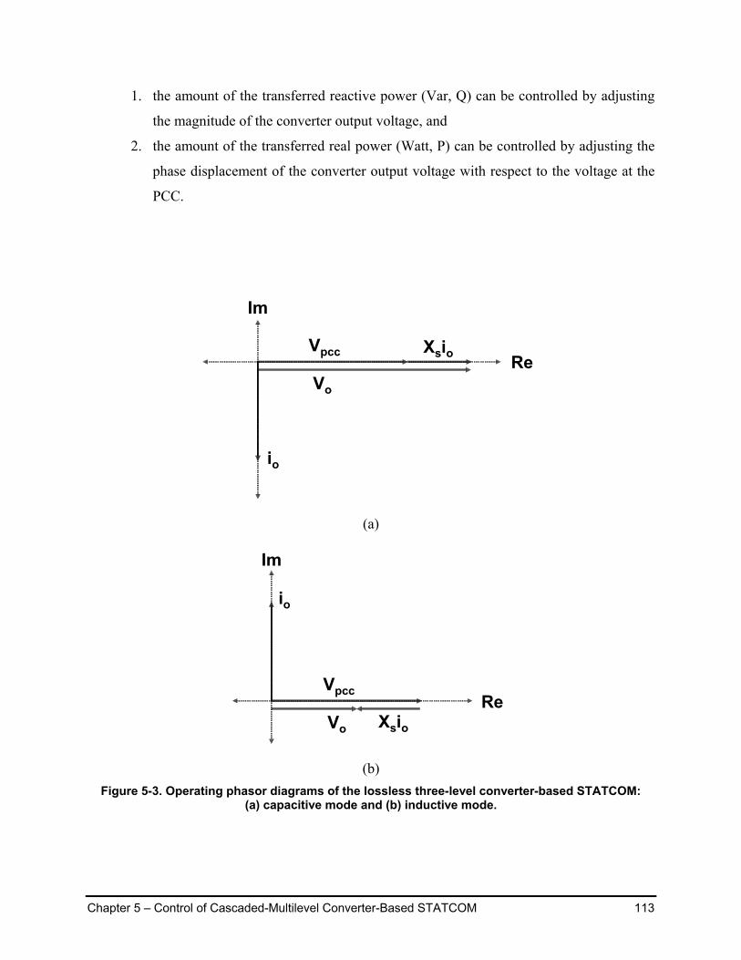
1. the amount of the transferred reactive power (Var, Q) can be controlled by adjusting
the magnitude of the converter output voltage, and
2. the amount of the transferred real power (Watt, P) can be controlled by adjusting the
phase displacement of the converter output voltage with respect to the voltage at the
PCC.
Vo
Vpcc Xsio
io
Im
Re
(a)
Vo
Vpcc
Xsio
io
Im
Re
(b) Figure 5-3. Operating phasor diagrams of the lossless three-level converter-based STATCOM:
(a) capacitive mode and (b) inductive mode.
Chapter 5 – Control of Cascaded-Multilevel Converter-Based STATCOM 114
Vo
Vpcc
Xsio
io
Im
Reδ
Figure 5-4. Operating phasor diagrams of non-ideal three-level converter-based STATCOM.
II. Three-Level Cascaded-Based STATCOM Control Design
The control design starts with the three-level cascaded converter, which has the least number
of output voltage levels. With only one H-bridge converter per phase, voltage-balancing problem
does not exist in this case. The purpose of starting with the three-level converter is to verify the
correctness and accuracy of the output currents and single DC capacitor voltage regulation.
This particular STATCOM system, as shown in Figure 5-5, is formed by a three-level
cascaded converter that is coupled to a power system by the coupling reactors at the PCC.
Three-levelCascaded Converter
Vpcc
io
~~PCC
Power System
VoC Loss Xs
Figure 5-5. Single-line diagram of a STATCOM system utilizing the three-level cascaded converter.
Chapter 5 – Control of Cascaded-Multilevel Converter-Based STATCOM 115
The schematic of the completed power stage of the three-level cascaded-based STATCOM is
shown in Figure 5-5. Each phase of the cascaded converter consists of an H-bridge converter,
which can generate three levels of output voltages, i.e., –E, 0 and +E.
Vsa
VsbVsc
Ns
LpRp
LpRp
LpRp
ipa
ipb
ipc
van vbn vcn
n
ia ib
ic
LsRs
LsRs
LsRs
Vpcca
Vpccb
Vpccc
Point of Common Coupling
Eb+_
SaNvb+_
Sb12
Sb14
Sb11
Sb13
Ea+_
SaNva+_
Sa12
Sa14
Sa11
Sa13
Ea+_
SaNva+_va+_
Sa12
Sa14
Sa11
Sa13
Ec+_
SaNvc+_
Sc12
Sc14
Sc11
Sc13
Ec+_
SaNvc+_vc+_
Sc12
Sc14
Sc11
Sc13
Cascaded Three-level Converter
Figure 5-6. Schematic of the three-level cascaded-based STATCOM system.
Ls +_ +_
Ls
+ _+ _
+_+_
+_+_+
_
+
_
Rs
Rs
qs iL ~ω
pccdv~
pccqv~
ds iL ~ω
di~
qi~
+_+_
EDd~
EDd~
+_+_
EDq~
EDq~
dv~
qv~_
3C
RE/3RL/3
E~
Ei~
qqqq
dddd
IdiD
IdiD~~
~~
++
+
++_+_
+_+_
Figure 5-7. Small-signal model of the three-level cascaded-based STATCOM.
Chapter 5 – Control of Cascaded-Multilevel Converter-Based STATCOM 116
Based on the proposed HBBB discussed in Chapter 3, the electrical parameters of the
cascaded three-level converter and the power network are designed as shown in Table 5-1.
TABLE 5-1. SPECIFICATION OF THE STUDIED SYSTEM.
Three-Level Cascaded Converter Individual DC Bus Voltage 2100 V ± 10% Total DC Bus Voltage 2100 V ± 10% Rated RMS Reactive Current 1250 A Capacitor Impedance (2.5m-j/(ω⋅10.5mF)) Ω Individual Switching Frequency/ Equivalent Switching Frequency
1 kHz/ 2 kHz
Power System Configuration Balanced Three-Phase Three-Wire Coupling Reactor Impedance (13m-jω⋅350µH) Ω PCC Line Voltage 2100 V
A. System Transfer Functions
From the generic CMC-based STATCOM model derived in Chapter 4, with one H-bridge
converter per phase, the simplified small-signal model for the three-level cascaded-based
STATCOM can be depicted as shown in Figure 5-7. Due to the three-phase three-wire
configuration, the 0-channel is omitted in this case.
Based on the small-signal model of the three-level cascaded-based STATCOM, five key
transfer functions used for control design are derived as follows:
Chapter 5 – Control of Cascaded-Multilevel Converter-Based STATCOM 117
• Control-to-Output-Current Transfer Function, Gidd and Giqq
1
)1(
~~
2
++
+==
PP
Zidd
d
didd
QSS
SK
di
G
ωω
ω ,
Equation 5-4
where
( )22ss
sidd LR
NERK
ω+= ,
( )s
ss
RLR
Q2
22 ω+= ,
( )s
ssP L
LR 22 ωω
+= , and
s
sz L
R=ω ,
and
1
)1(
~~
2
++
+==
PP
Ziqq
q
qiqq
QSS
SK
d
iG
ωω
ω ,
Equation 5-5
where
( )22ss
siqq LR
NERK
ω+= ,
( )s
ss
RLR
Q2
22 ω+= ,
( )s
ssP L
LR 22 ωω
+= , and
s
sz L
R=ω .
Chapter 5 – Control of Cascaded-Multilevel Converter-Based STATCOM 118
• Control-to-Cross-Coupling-Output-Current Transfer Function, Giqd and Gidq
1~~
2
++
==
PP
iqd
d
qiqd
QSS
K
d
iG
ωω
,
Equation 5-6
where
( )22ss
iqd LRLNEKω
ω+
−= ,
( )s
ss
RLR
Q2
22 ω+= ,
( )s
ssP L
LR 22 ωω
+= , and
s
sz L
R=ω .
Likewise,
1~~
2
++
==
PP
idq
q
didq
QSS
K
di
G
ωω
,
Equation 5-7
where
( )22ss
idq LRLNEKω
ω+
−= ,
( )s
ss
RLR
Q2
22 ω+= ,
( )s
ssP L
LR 22 ωω
+= , and
s
sz L
R=ω .
Chapter 5 – Control of Cascaded-Multilevel Converter-Based STATCOM 119
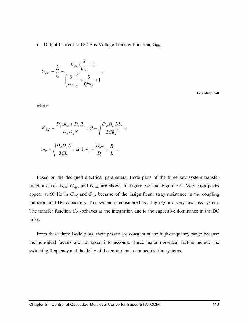
• Output-Current-to-DC-Bus-Voltage Transfer Function, GEid
1
)1(
~~
2
++
+==
PP
ZEid
dEid
QSS
SK
iEG
ωω
ω ,
Equation 5-8
where
NDDRDLD
Kqd
sdsqEid
+=
ω, 23 s
sqjdj
CR
NLDDQ = ,
s
qdP CL
NDD3
=ω , and s
s
d
qz L
RD
D+=
ωω .
Based on the designed electrical parameters, Bode plots of the three key system transfer
functions, i.e., Gidd, Giqq, and GiEd, are shown in Figure 5-8 and Figure 5-9. Very high peaks
appear at 60 Hz in Gidd and Giqq because of the insignificant stray resistance in the coupling
inductors and DC capacitors. This system is considered as a high-Q or a very-low loss system.
The transfer function GiEd behaves as the integration due to the capacitive dominance in the DC
links.
From these three Bode plots, their phases are constant at the high-frequency range because
the non-ideal factors are not taken into account. Three major non-ideal factors include the
switching frequency and the delay of the control and data-acquisition systems.
Chapter 5 – Control of Cascaded-Multilevel Converter-Based STATCOM 120
0.01 0.1 1 10 100 1 .103 1 .104 1 .1050
20
40
60
80
100
gain Gidd s fi( )( )( )
f fi( )
0.01 0.1 1 10 100 1 .103 1 .104 1 .105100
50
0
50
100
phase Gidd s fi( )( )( )
f fi( )
0.01 0.1 1 10 100 1 .103 1 .104 1 .1050
20
40
60
80
100
gain Giqq s fi( )( )( )
f fi( )
0.01 0.1 1 10 100 1 .103 1 .104 1 .105100
50
0
50
100
phase Giqq s fi( )( )( )
f fi( )
(a) (b)
Figure 5-8. Ideal open-loop transfer function of the control-to-output current in the (a) D-channel, Gidd, and (b) Q-channel, Giqq.
Chapter 5 – Control of Cascaded-Multilevel Converter-Based STATCOM 121
0.01 0.1 1 10 100 1 .103 1 .104 1 .105100
50
0
50
100
gain GEid s fi( )( )( )
f fi( )
0.01 0.1 1 10 100 1 .103 1 .104 1 .1050
50
100
150
phase GEid s fi( )( )( )
f fi( )
Figure 5-9. Ideal open-loop transfer function of the D-channel current-to-DC-capacitor voltage, GiEd.
B. Effects of Various Delays on the Transfer Functions
In practice, three important delays embedded in both the power stage and the controller must
be considered: the switching, the calculation and the transducer delays.
• Switching Delay Limited by the system operation condition and its thermal capability, the recent high-power
semiconductor devices can switch in a range of several hundred to a few kilohertz. The switching
delay is, therefore, the most important factor of concern in the high-power electronic control
design. To further explain how to determine the switching delay for the CMC, an H-bridge
converter, as shown in Figure 5-10, is used as an example. An H-bridge converter basically
consists of two phase legs. Each phase leg comprises two complementary switches. The
relationship of the total output voltage and individual phase-leg voltages is simply expressed as
follows:
Chapter 5 – Control of Cascaded-Multilevel Converter-Based STATCOM 122
)()()( tVtVtV RNLNLR −= .
Equation 5-9
Figure 5-11 shows the digital PWM synthesis for an H-bridge converter. The command duty
cycle is compared to a linear slope; the intersection determines the switching event. Each phase
leg is assumed to switch at 1/T Hertz. The left phase leg is controlled by the positive duty cycle,
whereas the right phase leg is controlled by the negative duty cycle, which is out of phase with
the positive duty cycle. The duty cycle is updated every half-cycle. In other words, each phase
leg responds to the duty cycle every half-cycle and has a half-cycle delay time. In Figure 5-11,
the duty cycle is updated at times T and 1.5 T. Although VLR(t) has twice the switching
frequency compared to each phase leg, the duty cycle is still updated every half-cycle. The
double switching frequency provides improvement in the synthesized output waveform, but it
does not shorten the delay time. Since the output of the CMC is the summation of N individual
H-bridge converters, its switching delay is then:
sswd fN
tT⋅⋅
=2
1)(_ .
Equation 5-10
E+
-E+
-
VLN(t)VRN(t)
N
VLR(t)+
-
Figure 5-10. Two phase legs forming an H-bridge converter.
Chapter 5 – Control of Cascaded-Multilevel Converter-Based STATCOM 123
TD
D(t)
T 2T1.5T
t(s)
VLN(t)
TD−t(s)
TD 5.1
TD 5.1−
t(s)
VRN(t)
VAN(t)
Figure 5-11. PWM-generation technique for the H-bridge converter.
• Calculation Delay This delay is basically a function of the processor used in the controller. Due to its high-
speed arithmetic units, the recent floating-point DSP is widely employed in real-time control
applications. In this dissertation, a 133MHz DSP from Texas Instrument (TI), TMS320D6701,
which can perform 800 mega floating-point operations per second (MFLOPS), is programmed to
finish each feedback calculation in 100 µs. The calculation delay is thus:
Chapter 5 – Control of Cascaded-Multilevel Converter-Based STATCOM 124
stT cald µ100)(_ = .
Equation 5-11
• Transducer Delay In general, feedback parameters in a digital-based control system are acquired by analog-to-
digital converters (ADCs). The transducer delay is also known as the sampling delay, which is
indirectly proportional to the sampling frequency of the ADC. An ADC from TI, THS1206, is
used as the data converters in this dissertation. It has 12 bits of resolution and a conversion rate
of 6 megasamples per second (MSPS). The transducer delay is therefore 167 ns.
nstT ADCd 167)(_ = .
Equation 5-12
• Total Delay Basically, the total delay is the summation of these three previously discussed delays. Due to
the dominance of the switching delay, the total delay time can be approximated by the switching
delay, as shown in Equation 5-13.
swdADCdcaldswdd TTTTT ____ ≈++= .
Equation 5-13
This delay mainly affects the phase delay of the loop gain, and can be modeled in Laplace
form as follows:
STdeS −=)(τ .
Equation 5-14
By taking into account the system delay, the new open-loop transfer function, Gidd, can be
plotted as shown in Figure 5-12. With a switching frequency of 1 kHz, the phase of Gidd rapidly
rolls off at above 70 Hz. Obviously, this significantly limits the bandwidth of the feedback-
current loop gain. Based on the controller processor and power stage of the converter, the
switching delay has the most significant effect on the control design.
Chapter 5 – Control of Cascaded-Multilevel Converter-Based STATCOM 125
0.01 0.1 1 10 100 1 .103 1 .104 1 .1050
20
40
60
80
100
gain Gidd s fi( )( )( )gain Gidd_delay s fi( )( )( )
f fi( )
0.01 0.1 1 10 100 1 .103 1 .104 1 .105200
100
0
100
200
phase Gidd s fi( )( )( )phase Gidd_delay s fi( )( )( )
f fi( )
Figure 5-12. Comparison of the transfer function, Gidd, without and with delay.
C. Cross-Coupling Effects
To show the cross-coupling components between the D-channel and the Q-channel, the
differential equation of the output current of the STATCOM is rewritten in Equation 5-15:
Chapter 5 – Control of Cascaded-Multilevel Converter-Based STATCOM 126
⋅
−
−
−
+
=
00000~~~
00
0
0
~~~
1~
~~~
~~~
iii
LR
LR
LR
vvv
LDDD
LE
ddd
LE
iii
dtd
q
d
s
s
s
s
s
s
vpcc
vpccq
vpccd
sq
d
sq
d
sq
d
ω
ω
.
Equation 5-15
From Equation 5-15, in the D-channel, a current-controlled voltage source is a function of the
current iq, while, in the Q-channel, a current-controlled-voltage source is a function of cross-
coupling current, id. The amplitudes of both dependent voltage sources can be expressed in
Equation 5-16:
qdq iLv ⋅⋅= ω ,
and
dqd iLv ⋅⋅= ω .
Equation 5-16
To show the cross-coupling effect, the Bode plot of Gidd and Giqd are illustrated in Figure
5-13. Obviously, at frequencies lower than the corner frequency, which is roughly 60 Hz, the
gain of Giqd dominates that of Giqd. In other words, by controlling duty cycle d, the Q-channel
current tends to react more than the D-channel current does, which is undesirable.
In order to alleviate the cross-coupling effect, the designed crossover frequency of the current
closed-loop gain should be kept higher than the corner frequency, where the gain of Gidd is
higher than that of Giqd. To further improve the loop response, the decoupling technique is
applied in the current loop gain, as discussed in the following section.
Chapter 5 – Control of Cascaded-Multilevel Converter-Based STATCOM 127
Figure 5-16. Phasor diagram of the alignment of key control parameters.
This obviously complies to the control law presented earlier, i.e., the amount of transferred
reactive power (Var, Q) can be controlled by adjusting the magnitude of the converter output
voltage, and the amount of transferred real power (Watt, P) can be controlled by adjusting the
phase displacement of the converter output voltage with respect to the voltage at the PCC.
Chapter 5 – Control of Cascaded-Multilevel Converter-Based STATCOM 132
E. Feedback-Controller Design
Figure 5-17 shows the complete proposed control block diagram for the three-level cascaded-
based STATCOM system. The main objective of the feedback controller is to regulate the Q-
channel current following its command as fast as possible.
Gidq
Giqd
ΣΣ
ΣΣ Iq
GEid
++
++Giqq
Gidd
dq*
dd* Id
E
Hid
Hiq
ΣΣ+
_
HEdΣΣ+
_
ΣΣ+ _
id*
iq*
E*
Cascaded Three-Level STATCOM Model
Controller
ΣΣ+
_
ΣΣ
ωL/E
+
+ωL/E
Cascaded Three-Level Based STATCOM System
Figure 5-17. Control block diagram.
This discussion will begin with the D-channel. In the D-channel, there are two main control
loops: the internal output current loop (Id-loop) and the external voltage loop (E-loop). The
output of the voltage loop is the reference for the Id-loop. In the E-loop, the three DC capacitor
voltages are averaged and compared to the reference, which is fixed at 2100 V. The error is
compensated by the voltage compensator, HE. The output of HE is then used as the command for
the Id-loop. For the Id-loop, the Id command is compared with the feedback Id, and its error is the
input of the current regulator, Hid. Finally, the output of the current regulator is the D-channel
duty cycle command.
In the Q-channel, the Iq command is generated by an external control, which is obtained
either from the control person or the automatic controller. The Iq command is compared with the
Chapter 5 – Control of Cascaded-Multilevel Converter-Based STATCOM 133
feedback Iq, and the error is compensated by the current compensator, Hiq, whose output is the Q-
channel duty cycle command.
The control process starts with the internal control loop. The current compensators Hid and
Hiq are first designed to meet the crossover frequency and phase margin requirement. In the D-
channel, the voltage compensator HEid is then designed based on the new current-loop gain.
• Design of Current Compensator, Hiq and Hiq Based on the designed power stage parameters, the Bode plots of the open-loop transfer
functions Gidd and Giqq, associated with the delay, are shown in Figure 5-18. Because the
characteristics of Gidd and Giqq are identical, only Gidd is used throughout the current-compensator
design process.
0.01 0.1 1 10 100 1 .103 1 .104 1 .10505
101520253035404550556065707580859095
100
gain Gidd s fi( )( )( )
f fi( )
0.01 0.1 1 10 100 1 .103 1 .104 1 .105200
100
0
100
200
phase Gidd s fi( )( )( )
f fi( )
-180
0.01 0.1 1 10 100 1 .103 1 .104 1 .10505
101520253035404550556065707580859095
100
gain Giqq s fi( )( )( )
f fi( )
0.01 0.1 1 10 100 1 .103 1 .104 1 .105200
100
0
100
200
phase Giqq s fi( )( )( )
f fi( )
-180
(a) (b)
Figure 5-18. Open-loop control-to-output-current transfer function associated with delay in the (a) D-channel, Gidd (b) Q-channel, Giqq.
Chapter 5 – Control of Cascaded-Multilevel Converter-Based STATCOM 134
Due to the Nyquist’s criteria, the designed crossover frequency of the current loop should not
be higher than half of the effective switching frequency, which equals twice the individual
phase-leg switching frequency or 2 kHz in this case. Basically, an average model is capable of
predicting the behavior of its switching model from DC up to half of the effective switching
frequency. By designing the crossover frequency above this specific switching frequency, the
stability prediction of the system is theoretically invalid. From the Bode plot shown in Figure
5-18, the loop gain of the compensated Gidd at the low-frequency range should be as high as
possible, such that the output is well regulated at DC and at frequencies below the crossover
frequency.
Among well-known compensators, the lag compensator or the proportional-plus-integral (PI)
is the best candidate based on its simplicity and reliability. A general transfer function of the PI
compensator HPI(S) is given in Equation 5-21, and its magnitude and phase asymptotes are
shown in Figure 5-19. To achieve a zero steady-state error for the current-loop gain, an inverted
zero of the PI compensator is added at frequency fL. Moreover, if fL is sufficiently below the loop
crossover frequency, the original phase margin is not disturbed by the PI compensator.
+= ∞ S
HSH LPIPI
ω1)(
Equation 5-21
Chapter 5 – Control of Cascaded-Multilevel Converter-Based STATCOM 135
0.01 0.1 1 10 100 1 .103 1 .104 1 .10580
72
64
56
48
40
32
24
16
8
0
gain HPI s fi( )( )( )
f fi( )
0.01 0.1 1 10 100 1 .103 1 .104 1 .105100
90
80
70
60
50
40
30
20
10
0
10
phase HPI s fi( )( )( )
f fi( )
fL
-20 dB/decade
45°/decade
∞PIH
10fL
fL/10
Figure 5-19. Bode plot of the PI compensator transfer function.
Alternatively, the PI compensator can be expressed by its two sub-functions, i.e., proportion
and integral, as follows:
SKKSH i
pPI +=)( ,
Equation 5-22
where ∞= PIp HK , and LPIi HK ω⋅= ∞ .
According to the Bode plot of Gidd, as shown in Figure 5-18, a couple of undesirable factors
complicate the design of compensator Hid(S), i.e., very high Q in the gain and that the phase
quickly rolls off in the vicinity of the designed crossover frequency.
With the compensator, the closed-loop transfer function of the D-channel current can be
expressed as follows:
Chapter 5 – Control of Cascaded-Multilevel Converter-Based STATCOM 136
)()()( SGSHST iddidid ⋅= .
Equation 5-23
After the optimization process, the best-designed parameters for the PI compensator are
given in Table 5-2. The current-loop gain is plotted, as shown in Figure 5-20, to verify its
stability. The desired crossover is selected to be as high as possible, but must be less than 1 kHz,
which is half of the effective switching frequency. Due to the severe switching delay, the
designed crossover frequency is 200 Hz, with reasonably large phase margin of 50 degrees. The
characteristics of current loop gain Tid(S) are listed in Table 5-2. Due to having a transfer
function identical to that of the D-channel current, the Q-channel-current loop compensator
Hiq(S) is designed, and its closed-loop magnitude and phase are plotted in Figure 5-21.
TABLE 5-2 DESIGNED PI COMPENSATOR PARAMETERS AND CURRENT LOOP GAIN CHARACTERISTICS.
Parameters Values PI Compensator, Hid(S) Kp 2.12×10⁻⁴ Ki 6.00×10⁻³ Loop Gain Tid(S) Characteristic Crossover Frequency (Hz) 200 Phase Margin (degrees) 50 Gain Margin (dB) 7.7
Chapter 5 – Control of Cascaded-Multilevel Converter-Based STATCOM 137
Figure 5-23. Bode plot of the reference current-to-DC voltage transfer function, TEid(S).
TABLE 5-3. DESIGNED PI COMPENSATOR PARAMETERS AND VOLTAGE-LOOP GAIN CHARACTERISTICS.
Parameters Values PI Compensator, HEd(S) Kp 1.75 Ki 550 Loop Gain TEd(S) Characteristics Crossover Frequency (Hz) 20 Phase Margin (degree) 158 Gain Margin (dB) 53.8
Chapter 5 – Control of Cascaded-Multilevel Converter-Based STATCOM 141
0.01 0.1 1 10 100 1 .103 1 .104 1 .105150
100
50
0
50
100
150
gain TEd s fi( )( )( )
f fi( )
0.01 0.1 1 10 100 1 .103 1 .104 1 .105200
100
0
100
200
phase TEd s fi( )( )( )
f fi( )
22.2°
-180°
-53.8 dB°
20 Hz
Figure 5-24. Bode plot of closed-loop D-channel voltage loop, TEd(S).
F. Simulation Results of the Average Model with the Designed Control
To verify the stability and performance of the proposed control parameters, the average
model of the three-level cascaded-based STATCOM with the designed feedback control is
simulated. At the PCC, the power exchange between the STATCOM and the power network is
defined, and is divided into the following three modes for the particular simulation:
1. standby mode is the mode in which the STATCOM generates zero real and reactive
power (P = 0 Watt and Q = 0 Var),
Chapter 5 – Control of Cascaded-Multilevel Converter-Based STATCOM 142
2. inductive mode is the mode in which the STATCOM absorbs the reactive power from
the power network (at full inductive mode, P = 0 Watt and Q = -1.5 MVar), and
3. capacitive mode is the mode in which the STATCOM injects the reactive power into
the power network (at full capacitive mode, P = 0 Watt and Q = +1.5 MVar).
In this simulation, the STATCOM is commanded to operate in the following four modes:
1. at time 0 to 200 ms, the STATCOM operates in the standby mode, Iq = 0 A,
2. at time 200 ms to 400 ms, the STATCOM operates in the full inductive mode,
Iq = 2165 A,
3. at time 400 ms to 600 ms, the STATCOM still operates in the inductive mode, except
with a voltage sag at the PCC of 30% instead of the normal voltage, and
4. after 600 ms, the STATCOM operates in the full capacitive mode, Iq = -2165 A.
The command Iq at the full load is calculated from the full-load output current in the ABC
coordinate. The relationship between the AC parameters in the DQ0 and ABC coordinates yields
the following:
)(23)( _ titi pkAQ ⋅= ,
Equation 5-26
where iA-pk(t) is the peak of the output-phase current.
Figure 5-25 shows the simulation results of the STATCOM operating in these four modes.
The results indicate that the STATCOM stably operates for the entire range. The Q-channel
output current closely follows the command. The average DC capacitor voltage is also regulated
fairly well. At each transition period, the details of the simulation results are discussed and
verified.
Chapter 5 – Control of Cascaded-Multilevel Converter-Based STATCOM 143
Figure 5-25. Transient and steady-state responses of the proposed average model of three-level cascaded-based STATCOM with the designed feedback control operating in standby mode, full inductive mode, inductive mode under 30% voltage sag at the PCC and capacitive mode.
• Transition 1: from Mode 1 to Mode 2 At time 200 ms, the STATCOM is commanded to abruptly change its operation mode from
standby to full inductive mode by adjusting the Iq command from 0 to 2165 A. Due to the
assigned current direction during the modeling procedure, the output current leads the VPCC by
90° in the inductive mode and lags the VPCC by 90° in the capacitive mode. In mode 2, the
simulation result verifies that phase-A output current, ia, leads VPCC by 90°. The overshoot of Iq
is 32%.
Chapter 5 – Control of Cascaded-Multilevel Converter-Based STATCOM 144
Figure 5-26. The STATCOM responds to the step change from standby mode (mode 1) to full inductive mode (mode 2) at 0.2 S.
• Transition 2: from Mode 2 to Mode 3 At this particular transient, while the STATCOM is commanded to absorb full reactive power
from the power grid, at 400 ms, the three phase voltages at the PCC drop to 70% of the rated
line-to-line voltage, which is 1470 VRMS. Figure 5-27 illustrates the simulated transient of the
STATCOM. The command Iq is set at the full inductive mode for the entire transition. The
current Iq very fast responds to the transient in the PCC voltage, and settles in the 5%-error range
in 5 ms. The simulation results also show that the phase-A output current indicates the transient
and goes to steady state very quickly.
Chapter 5 – Control of Cascaded-Multilevel Converter-Based STATCOM 145
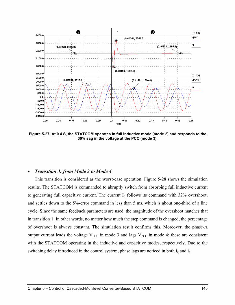
Figure 5-27. At 0.4 S, the STATCOM operates in full inductive mode (mode 2) and responds to the 30% sag in the voltage at the PCC (mode 3).
• Transition 3: from Mode 3 to Mode 4 This transition is considered as the worst-case operation. Figure 5-28 shows the simulation
results. The STATCOM is commanded to abruptly switch from absorbing full inductive current
to generating full capacitive current. The current Iq follows its command with 32% overshoot,
and settles down to the 5%-error command in less than 5 ms, which is about one-third of a line
cycle. Since the same feedback parameters are used, the magnitude of the overshoot matches that
in transition 1. In other words, no matter how much the step command is changed, the percentage
of overshoot is always constant. The simulation result confirms this. Moreover, the phase-A
output current leads the voltage VPCC in mode 3 and lags VPCC in mode 4; these are consistent
with the STATCOM operating in the inductive and capacitive modes, respectively. Due to the
switching delay introduced in the control system, phase lags are noticed in both iq and ia.
Chapter 5 – Control of Cascaded-Multilevel Converter-Based STATCOM 146
Figure 5-28. The STATCOM responds to the step change from full inductive mode (mode 3) to full capacitive current (mode 4).
G. Proposed Control System for Three-level Cascaded-Based STATCOM
After being verified by the average model, the feedback-parameter acquisition must be
modified before being applied in the real electrical circuit of the STATCOM in which all
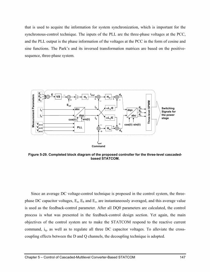
parameters are in the ABC coordinates. Figure 5-29 presents the completed block diagram of the
proposed controller for the three-level cascaded-based STATCOM. Additions to the control
designed for the average model of the three-level cascaded-based STATCOM are as follows: a
Park’s transformation, an inversed Park’s transformation, a PWM generator and a phase lock
loop (PLL). All feedback parameters are measured by using the signal transducers. Originally,
these feedback signals are in ABC coordinates. With the proposed control technique, all signals
are real-time transferred into DQ0 domain by Park’s transformation matrix2. The PLL is the tool
2 Derivation of the specific version of the Park’s transformation matrix used in this dissertation is shown in Appendix A.
Chapter 5 – Control of Cascaded-Multilevel Converter-Based STATCOM 147
that is used to acquire the information for system synchronization, which is important for the
synchronous-control technique. The inputs of the PLL are the three-phase voltages at the PCC,
and the PLL output is the phase information of the voltages at the PCC in the form of cosine and
sine functions. The Park’s and its inversed transformation matrices are based on the positive-
sequence, three-phase system.
HidHid
idref
+ _
id
dd
Hiq+
_
dq
iq
_
++
+
ωLs/E
ωLs/E
HEHE+
Eref
-1
Thre
e-le
vel S
PWM
abc
dqo
abc
dqo
PLL
cos(θ)
ia
ib
VpccaVpccbVpccc
Mea
sure
men
t Par
amet
ers
iqrefCommand
ΣΣ 1/31/3E
Ea
Eb
sin(θ)
HiqHiq
cos(θ) sin(θ)
Ec
abc
dqo
abc
dqodadbdc
Σ_
SwitchingSignals for the power stage
Figure 5-29. Completed block diagram of the proposed controller for the three-level cascaded-based STATCOM.
Since an average DC voltage-control technique is proposed in the control system, the three-
phase DC capacitor voltages, Ea, Eb and Ec, are instantaneously averaged, and this average value
is used as the feedback-control parameter. After all DQ0 parameters are calculated, the control
process is what was presented in the feedback-control design section. Yet again, the main
objectives of the control system are to make the STATCOM respond to the reactive current
command, iq, as well as to regulate all three DC capacitor voltages. To alleviate the cross-
coupling effects between the D and Q channels, the decoupling technique is adopted.
Chapter 5 – Control of Cascaded-Multilevel Converter-Based STATCOM 148
The products of the feedback control are the duty cycles in the DQ0 coordinates: Dd, Dq and
D0. Since the STATCOM is connected to the three-phase, three-wire power network, the zero
channel can therefore be omitted. Consequently, D0 is set to zero. To be able to control the power
stage of the STATCOM, the duty cycles must be transferred back into the ABC coordinates.
Once the duty cycle in ABC coordinates, which are Da, Db and Dc, are calculated, these three
duty cycles are used as the input of the PWM generator in order to produce the proper switching
signals for the power stage.
H. Simulation Results of the Cascaded Three-Level STATCOM with the Designed Controller
Based on the small-signal model of the three-level cascaded-based STATCOM, the
feedback-control parameters are designed, as discussed in the feedback-control design section,
and are applied in the completed electrical model of the proposed STATCOM in which the ideal
switch and diode models are utilized. In addition, all parasitic components and power-stage
losses are taken into account in the circuit.
• Comparison of Simulation Results of the Average and Electrical Models To verify the accuracy of the average model and the performance of the proposed control
system, a set of simulations, which uses the STATCOM power electronics model as the
reference, is performed. In the first simulation, the STATCOM is commanded to abruptly go
from the standby mode to the full capacitive mode, and its simulation results are shown in Figure
5-30. Three major parameters are compared between the results from the average model and
those from the electrical model: the Q-channel output current, Iq, the average DC capacitor
voltage, e_avg, and the output current of phase A, Ia. Due to the switching action in the electrical
model, the switching ripple appears in the simulation results.
In this case, the insignificant errors of the overshoot in Iq and e_avg are 0.7% and 0.25%,
respectively. In Figure 5-30(c), the results show that by neglecting the switching ripple, the
dynamic response of the phase-A output current can be very well represented by that of the
average output current of phase A.
Chapter 5 – Control of Cascaded-Multilevel Converter-Based STATCOM 149
0.7% error
(a)
0.25% error
(b)
(c)
Figure 5-30. Comparison between average model and electrical model of the STATCOM operating in the standby to full inductive modes: (a) Iq responses, (b) average DC capacitor voltages, and (c)
output currents.
Chapter 5 – Control of Cascaded-Multilevel Converter-Based STATCOM 150
2.5% error
(a)
0.7% error
1.2% error
(b)
(c)
Figure 5-31. Comparison between average model and electrical model of the STATCOM operating in the full capacitive to full inductive modes: (a) Iq responses, (b) average DC capacitor voltages,
and (c) output currents.
Chapter 5 – Control of Cascaded-Multilevel Converter-Based STATCOM 151
The second simulation is for the worst-case operation in which the STATCOM is controlled
to respond to the step command from full capacitive to full inductive modes. The simulation
results are shown in Figure 5-31. In this case, the error of the overshoot in of Iq and e_avg are
2.5% and 1.2%, respectively. Again, the results show that, by neglecting the switching ripple, the
dynamic response of the phase-A output current can be predicted by that of the average output
current of phase A.
In conclusion, the results indicate that the proposed average model is very accurate and can
very closely predict the dynamic behaviors of the three-level cascaded-based STATCOM.
• Simulation Results of the Electrical Model with the Proposed Controller To further verify the stability and performance of the proposed STATCOM controller, more
continuous operation modes are simulated. The STATCOM is commanded to operate in the
following six modes:
1. at time 0 to 100 ms, the STATCOM operates in the standby mode, Iq = 0 A, and Ia = 0 ARMS,
2. at time 100 ms to 300 ms, the STATCOM operates in the full inductive mode, Iq = +2165 A, and Ia = -1250 ARMS,
3. at time 300 ms to 500 ms, the STATCOM operates in the full capacitive mode, Iq = -2165 A and Ia = +1250 ARMS,
4. at time 500 ms to 700 ms, the STATCOM again operates in the full inductive mode, Iq = +2165 A, and Ia = -1250 ARMS,
5. at time 700 ms to 900 ms, the STATCOM operates in the half inductive mode, Iq = +1083 A, and Ia = -625 ARMS, and
6. after 900 ms, the STATCOM finally returns to the standby mode.
The simulation results of the STATCOM operating in these six modes are illustrated in
Figure 5-32. As shown, the STATCOM stably operates for the entire range. In general, the Q-
channel output current, iq, very closely follows its command. The average DC voltage is also
Chapter 5 – Control of Cascaded-Multilevel Converter-Based STATCOM 152
regulated fairly well. Five interesting transitions occur in this simulation. Detailed simulation
results are discussed and verified.
Figure 5-32. Transient and steady-state responses of the three-level cascaded-based STATCOM with the proposed feedback controller, operating in standby mode, full inductive mode, full
capacitive mode, full inductive mode, half capacitive mode and standby mode.
The detail of the transition from modes 2 to 3 is shown in Figure 5-33(a). The STATCOM
operation transfers from the full inductive to the full capacitive modes. The current iq very
quickly follows the command. The current ia simultaneously transfer from 90° leading to 90°
lagging Vpcc in less than half a line cycle. The results also show that all three DC capacitor
voltages are very well regulated during the transient and steady states. The detail of the
STATCOM response to the command to go from full capacitive to full inductive modes is
Chapter 5 – Control of Cascaded-Multilevel Converter-Based STATCOM 153
illustrated in Figure 5-34(b). From the simulation results, the voltage ripple of the DC capacitor
in the inductive mode is slightly less than that of the capacitive mode due to the different amount
of average current flowing into the DC capacitor. As mentioned in the converter modeling
process, the capacitor current is a product of the output current and the duty cycle of the
converter. Basically, the duty cycle in the inductive mode is less than that in the standby mode,
whereas the duty cycle in the capacitive mode is greater than that in the standby mode. In other
words, the duty cycle of the converter during the inductive mode is always less than that in the
capacitive mode. As a result, with the same amount of output current, the average amount of the
DC capacitor current during the inductive mode is always less than that of the capacitive mode.
Therefore, the capacitor needs to be designed to handle the worst-case voltage ripple, which
occurs when the STATCOM operates in the capacitive mode.
Chapter 5 – Control of Cascaded-Multilevel Converter-Based STATCOM 154
(a)
(b)
Figure 5-33. The STATCOM responds to the step change (a) from full inductive mode (mode 2) to full capacitive mode (mode 3) at 0.3 S, and (b) from full capacitive mode (mode 3) to full inductive
mode (mode 4) at 0.5 S.
Chapter 5 – Control of Cascaded-Multilevel Converter-Based STATCOM 155
(a)
(b)
Figure 5-34. The STATCOM responds to the step change (a) from full inductive mode (mode 4) to half capacitive mode (mode 5) at 0.7 S, and (b) from half capacitive mode (mode 5) to standby
mode (mode 5) at 0.9 S.
At 0.7 s, the STATCOM is commanded to generate a half-rated reactive current in mode 5
following mode 4. The simulation results for this transition are shown in Figure 5-34(a). The
Chapter 5 – Control of Cascaded-Multilevel Converter-Based STATCOM 156
current is decreased from full to half rating following the command. All three capacitor voltages
go to the steady state in about 0.2 s. The last transition at 0.9 s is shown in Figure 5-34(b). The
STATCOM is finally commanded to go back to the standby mode in which it exchanges no
power with the power network. The average STATCOM output current becomes zero, although
the switching ripple in the current still exists. The three capacitor voltages go back to the
reference with no ripple, which indicates that there is no reactive power circulating in the
capacitors.
Figure 5-35 shows voltage and current waveforms for a transient period of the STATCOM
transferring from full capacitive to full inductive modes. The phase-A output voltage of the
STATCOM is almost always in phase with the voltage at the PCC. A small phase shift is,
however, applied when the capacitor voltages need to be adjusted. In addition, the results verify
that all three capacitor voltages and three output currents are very well regulated. According to
the control design criteria, the response of the DC-voltage loop is about 10 times slower than that
of the output-current loops. As a result, the DC capacitor voltages go to the steady state
approximately 10 times later than the output currents do.
FullCapacitive
FullInductive
Figure 5-35. Waveforms of the STATCOM system transitioning from the full capacitive to full inductive modes.
Chapter 5 – Control of Cascaded-Multilevel Converter-Based STATCOM 157
I. Experimental Validation
To firmly verify the proposed STATCOM model and feedback controller, a real-time IGBT-
based STATCOM testbed3 is implemented. The STATCOM testbed is basically composed of
three parts: the IGBT-based CMC, the DSP-based controller, and the passive components. The
schematic of the testbed is shown in Figure 5-36. The reactive current command is fed into the
controller though the user interface. The feedback parameters are measured by the analog
transducers, and are converted to digital domain by the ADCs. The feedback-control routine is
coded and downloaded to the program memory of the DSP.
Vpcc
∼∼ CascadedMultilevelConverter
DSP-BasedController
User Interface
Iout E
Autotransformer
ACSource
XSXP
Figure 5-36. The schematic of the STATCOM testbed.
• Testbed Power Stage Operating Parameters The operating point of the testbed is selected based on the limitation of the laboratory
facilities. The main switching device is the IGBT in which a freewheeling diode is internally
connected in parallel. To properly verify the proposed models, the constraints of the testbed
3 Details of the STATCOM testbed are given in Appendix B.
Chapter 5 – Control of Cascaded-Multilevel Converter-Based STATCOM 158
power stage are kept identical to those of the high-power system. Those parameters are as
follows:
1. the switching frequency,
2. the dead-time, and
3. the percentage of the DC capacitor voltage ripple.
Table 5-4 shows the final parameters of the testbed operating point. The three-phase AC
input voltages are transformed from 208 V to 100 V by the autotransformer. The switching
frequency is kept at 1 kHz. The DC capacitor voltage ripple at the full capacitive load is 10%.
The coupling reactor impedance is the combination of the leakage inductance of the
autotransformer and the additional inductors.
TABLE 5-4. SPECIFICATIONS OF THE TESTBED AT THE OPERATING POINT.
Three-Level Cascaded Converter Individual DC Bus Voltage 100 V ± 10% Total DC Bus Voltage 100 V ± 10% Rated RMS Reactive Current 10 A Capacitor Impedance (0.5m-j/(ω⋅2.0mF)) Ω/Phase Individual Switching Frequency/ Equivalent Switching Frequency
1 kHz/ 2 kHz
Power System Configuration Balanced Three-Phase Three-Wire Coupling Reactor Impedance (72m-jω⋅2.0mH) Ω/Phase PCC Line Voltage 100 V
• Control System Parameters Besides the same constraint of the power stage, the control parameters are also designed in
such a way that the same bandwidths and phase margins are achieved for both the current and the
voltage loops. As a result, the percentages of the testbed responses are identical to those in the
high-voltage STATCOM system. Based on the same approach used in the simulation, the
designed control parameters for the testbed at the proposed operating point are given in Table
5-5.
Chapter 5 – Control of Cascaded-Multilevel Converter-Based STATCOM 159
TABLE 5-5. DESIGNED PI COMPENSATOR PARAMETERS AND CURRENT AND VOLTAGE-LOOP GAINS CHARACTERISTICS OF THE TESTBED.
Parameters Values Current Loop PI Compensator, Hid(S) Kp 0.021 Ki 6.0 Loop-Gain Tid(S) Characteristics Crossover Frequency (Hz) 200 Phase Margin (Degrees) 50 Gain Margin (dB) 8.7 Voltage Loop PI Compensator, HEd(S) Kp 0.477 Ki 150 Loop-Gain TEd(S) Characteristics Crossover Frequency (Hz) 20 Phase Margin (Degrees) 156 Gain Margin (dB) 51.1
To verify the designed loop-gain characteristics shown in Table 5-5, the Bode plots of both
current and voltage loop gains are illustrated in Figure 5-37 and Figure 5-38, respectively. The
crossover frequency of the current loop is designed at 200 Hz, with a phase margin of 50°, while
that of the voltage loop is at 20 Hz, with a phase margin of 156°.
Chapter 5 – Control of Cascaded-Multilevel Converter-Based STATCOM 160
Figure 5-37. Bode plots of the open-loop control-to-D-channel-current transfer function (dashed line) and the D-current loop gain (solid line) of the testbed at the operating point.
Chapter 5 – Control of Cascaded-Multilevel Converter-Based STATCOM 161
0.01 0.1 1 10 100 1 .103 1 .104 1 .105150
100
50
0
50
100
150
gain TEd s fi( )( )( )
f fi( )
0.01 0.1 1 10 100 1 .103 1 .104 1 .105200
100
0
100
200
phase TEd s fi( )( )( )
f fi( )
24.1°
-180°
-51.1 dB°
20 Hz
Figure 5-38. Bode plot of the reference current-to-DC voltage transfer function, TEd(S).
• Experimental Results The proposed feedback routine is digitally coded and downloaded to the program memory of
the DSP. The testbed system, as shown in Figure 5-36 is set up. Several experiments are
conducted.
Steady-State Compensation
The experimental results of the steady-state compensation in both capacitive and inductive
modes are shown in Figure 5-39(a) and (b), respectively. To show the capacitor and inductor
characteristics of the STATCOM, the direction of the STATCOM current in these experimental
Chapter 5 – Control of Cascaded-Multilevel Converter-Based STATCOM 162
results is from the power network to the STATCOM, which is opposite to that in the simulation.
From Figure 5-39(a), the 10%, 120Hz ripple is noticed on top of the DC capacitor voltage, EA.
Again, to minimize the DC capacitance, an expectable voltage ripple must be allowed. The
output current of phase A, iA, leads the line voltage Vpcc AB by 60°. In other words, the phase-A
voltage at the PCC lags the current iA by 90°, which is consistent with the simulation results.
In the inductive mode, as shown in Figure 5-39(b), the current iA lags the line voltage Vpcc AB
by 120°, which agrees with the simulation results. As explained in the simulation results, the
experimental results indicate that the voltage ripple of the DC capacitor in the inductive mode is
The experimental results of the STATCOM responding to the step command from standby to
full capacitive mode is shown in Figure 5-40. The DC capacitor voltage, EA, is very well
regulated during the transient. After the transient, as shown in Figure 5-40(a), the current iA lags
the line voltage Vpcc AB by 120°. In other words, the phase-A voltage at the PCC leads the
current iA by 90°, which is consistent with the simulation results. In Figure 5-40(b), the DC
Chapter 5 – Control of Cascaded-Multilevel Converter-Based STATCOM 163
voltage EA is shown in detail. The peak-to-peak ripple voltage is about 10 V, which is 10% of the
DC voltage setting of 100 V.
Transition from Full Capacitive to Full Inductive Mode and Vice Versa
The simulation results, as illustrated in Figure 5-41, validate the stability and the
performance of the proposed control system reacting to the worst-case commands. The
STATCOM is commanded to go from full capacitive to full inductive modes and vice versa, as
shown in Figure 5-41(a) and (b), respectively. The voltage EA is very finely regulated during
both transitions and steady states. The output current iA responds very quickly to the step
command, and goes smoothly to the steady state.
Chapter 5 – Control of Cascaded-Multilevel Converter-Based STATCOM 164
Iq*
EA(200 V/DIV)
Vpcc AB(150 V/DIV)
iA(10 A/DIV)
10 ms/DIV
(a)
EA(5 V/DIV)
VAB(200 V/DIV)
10 ms/DIV
(b)
Figure 5-40. Experimental results of the testbed responding to a step command from standby to full capacitive mode: (a) DC capacitor voltage of phase A (EA), the voltage at the PCC between
phases A and B (Vpcc AB), phase A output current (iA) and the reactive current command (Iq*) and (b) the detail of EA and the output line-to-line voltage of the cascaded three-level converter (VAB).
Chapter 5 – Control of Cascaded-Multilevel Converter-Based STATCOM 165
Iq*
EA(200 V/DIV)
Vpcc AB(150 V/DIV)
iA(15 A/DIV)
10 ms/DIV
(a)
Iq*
EA(200 V/DIV)
Vpcc AB(150 V/DIV)
iA(15 A/DIV)
10 ms/DIV
(b)
Figure 5-41. The experimental results of the DC capacitor voltage of phase A (EA), the voltage at the PCC between phases A and B (Vpcc AB), phase A output current (iA) and the reactive current
command (Iq*) of the testbed responding to a step command: (a) from full capacitive to full inductive mode and (b) from full capacitive to full inductive mode.
Chapter 5 – Control of Cascaded-Multilevel Converter-Based STATCOM 166
Periodic Transition from Standby Mode to full capacitive Mode and Vice Versa
In this experiment, the STATCOM is commanded to generate the pulsating reactive power,
which is generally required in the flicker-mitigation applications. The frequency of the pulsating
power is set at 5 Hz. As shown in Figure 5-42(a), the STATCOM injects the full capacitive
current for 100 ms and no current for another 100 ms. The capacitor voltage, EA, is kept constant
by the feedback voltage loop. Figure 5-42(b) illustrates the detail of the DC capacitor voltage and
the output voltage of the converter. The 10% voltage ripple of voltage EA can be noticed during
the full capacitive compensation. From full capacitive to standby mode, voltage EA goes back to
the setting value. Due to the lack of compensated current, there is no ripple across the capacitor
during the standby mode.
Chapter 5 – Control of Cascaded-Multilevel Converter-Based STATCOM 167
Iq*
EA(200 V/DIV)
Vpcc AB(150 V/DIV)
iA(10 A/DIV)
20 ms/DIV
(a)
EA(10 V/DIV)
VAB(200 V/DIV)
40 ms/DIV
(b)
Figure 5-42. The STATCOM generates pulsating reactive power: (a) the DC capacitor voltage of phase A (EA), the voltage at the PCC between phases A and B (Vpcc AB), phase A output current (iA) and the reactive current command (Iq*) and (b) the details of EA and the converter output voltage
(VAB).
Convergence of Three DC Capacitor Voltages, EA, EB and EC
This experiment is to verify the convergence of all three DC capacitor voltages, EA, EB and
EC. The experimental results, as shown in Figure 5-43, demonstrate that during both full
Chapter 5 – Control of Cascaded-Multilevel Converter-Based STATCOM 168
capacitive and standby modes, all three DC capacitor voltages are well regulated and converge to
the reference, which is 100 V in this case. Moreover, the extreme case is shown in Figure 5-44,
in which the STATCOM periodically operates between full capacitive and full inductive modes.
Again, all three DC capacitors are well regulated and converge to the reference.
EA , EB , EC(10 V/DIV)
iA(10 A/DIV)
Figure 5-43. The STATCOM goes from full capacitive to standby mode.
100 V
Full CapacitiveFull Inductive
IA (10A/DIV)
EA , EB , EC
Figure 5-44. The STATCOM goes from full capacitive to full inductive mode and vice versa.
Chapter 5 – Control of Cascaded-Multilevel Converter-Based STATCOM 169
J. Summary
Based on the assumption of the effective DC voltage-balancing technique, the accuracy of
the proposed model of the CMC-based STATCOM was initially validated by both simulation
and experimental results obtained by the STATCOM utilizing the cascaded three-level converter.
The experimental results are consistent with the simulation results.
In the high-voltage STATCOM system, due to the limitation of the recent power
semiconductor device technology, a higher number of voltage levels is required in the CMC
topology. Besides improving the voltage capability, several other advantages can be achieved by
utilizing the CMC in STATCOM applications. With the knowledge acquired from the cascaded
three-level converter results, the performance of the STATCOM system can be greatly improved
by the following factors: higher switching frequency, faster dynamic responses, better output-
waveform quality, and better redundancy and stability. However, it is not possible to achieve
these advantages in the CMC-based STATCOM, unless an effective voltage-balancing technique
is applied to its DC capacitor voltages.
III. DC Capacitor Voltage-Balance Control Approaches
A. Imbalance of DC Capacitor Voltages in the Cascaded-Multilevel Converter-Based STATCOM
Obviously, the primary attraction of the CMC topology is its modularity. However, this
topology requires an excessive amount of DC voltage sources. The most important factors
causing the voltage imbalance among these DC capacitors are the difference in the DC-link
utilizations, the power stage losses and the component tolerances. Figure 5-45, for example,
shows a phase leg of a cascaded seven-level converter. The resistor RLA1, RLA2 and RLA3,
represented the internal losses in the H-bridge converters in levels 1, 2 and 3, respectively. The
internal losses may be differently influenced by the switching and conduction activity and the
component tolerances. Firstly, these H-bridge converters are assumed to be lossless, and their
capacitor voltages have the same initial values. To achieve steady-state, balanced voltages, these
DC capacitors must have the same amount of real power utilization in a given period of time.
Due to sharing the same output current, the differences in the capacitor currents are caused by
the different duty cycles, because a capacitor current is a product of a duty cycle and an output
Chapter 5 – Control of Cascaded-Multilevel Converter-Based STATCOM 170
current. Therefore, the average switching functions or duty cycles in these H-bridge converters
must be identical or else different in the DC voltages will be introduced. A couple of suitable
modulation techniques can solve this problem.
EA3
+
_CC
iEb3iEb3
RLA3vA3+_vA3+_HBA3
EA2
+
_CC
iEb2iEb2
RLA2
HBA2
EA1
+
_CC
iEb1iEb1
RLA1
HBA1
iA
vA2+_vA2+_
vA1+_vA1+_
vAN
A
N
Figure 5-45. One phase leg of a seven-level cascaded converter.
The first technique, as shown in Figure 5-46(a), is called the rotating-pulse staircase, which is
suitable to be applied with high numbers of voltage levels. A seven-level case is used as an
example. Theoretically, the average amount of current flowing into and out of the capacitors is
equal after N/2 cycles, where N is the number of the H-bridge converters per phase. In a higher
number of voltage levels, this process, therefore, takes a longer time and introduces a voltage
ripple, whose frequency is 120/N Hz for the case of line frequency of 60Hz. Figure 5-46(b)
illustrates the second technique, called the phase-shifted carrier SPWM [10], which was
proposed to improve the quality of the output waveforms of the multi-converter modules in high-
voltage direct current (HVDC) applications. In the seven-level case, three carriers are 120° apart
Chapter 5 – Control of Cascaded-Multilevel Converter-Based STATCOM 171
from each other. Because of the use of equally distributed carrier signals, the fundamental
components of the waveforms in different levels are theoretically identical; therefore, the amount
of charges moving into and out of the capacitors in a period of time are equal.
VAN
VA3
VA2
VA1
t
t
t
t
(a)
For level 1 For level 2 For level 3
Modulating signal
(b)
Figure 5-46. PWM techniques equally utilizing the DC capacitor voltages: (a) rotating-pulse staircase and (b) phase-shifted carrier SPWM.
By applying one of these two techniques, the capacitor voltage can be balanced in the
lossless STATCOM system. This is, however, not true in the case of the real STATCOM system,
because the H-bridge converters are not identical. The internal losses and the component
Chapter 5 – Control of Cascaded-Multilevel Converter-Based STATCOM 172
tolerances are, for example, different. To proof this, a seven-level cascaded-based STATCOM,
as shown in Figure 5-47, is used as an example.
The specifications of an example STATCOM system are shown in Table 5-6. The internal
losses in the phase-A H-bridge converters are slightly different. Losses in the H-bridge
converters in levels 1, 2 and 3 are 0.1%, 0.5% and 1% of its full power rating, respectively. The
control proposed in the case of the three-level cascaded-based STATCOM is used in this study.
The phase-shifted carrier SPWM is used to generate the switching signals for the cascaded
seven-level converter. Basically, the same duty cycle is used for all three H-bridge converters in
the same phase leg, regardless to the amplitudes of their DC capacitors.
van vbn vcn
n
ia ib
ic
Vsa
VsbVsc
LsRs
LsRs
LsRs
Ns
Vpcca
Vpccb
Vpccc
Point of Common Coupling
Eb3+_
SaNvb3+_
Sb32
Sb34
Sb31
Sb33
Ea3+_
SaNva3+_
Sa32
Sa34
Sa31
Sa33
Ea3+_
SaNva3+_va3+_
Sa32
Sa34
Sa31
Sa33
Ec3+_
SaNvc3+_
Sc32
Sc34
Sc31
Sc33
Ec3+_
SaNvc3+_vc3+_
Sc32
Sc34
Sc31
Sc33
Eb2+_ vb2
+_
Sb22
Sb24
Sb21
Sb23
Ea2+_ va2
+_va2+_
Sa22
Sa24
Sa21
Sa23
Ec2+_ vc2
+_vc2+_
Sc22
Sc24
Sc21
Sc23
Eb1+_ vb1
+_
Sb12
Sb14
Sb11
Sb13
Ea1+_ va1
+_va1+_
Sa12
Sa14
Sa11
Sa13
Ec2+_ vc1
+_vc1+_
Sc12
Sc14
Sc11
Sc13
Seven-level Cascaded Converter
LpRp
LpRp
LpRp
ipa
ipb
ipc
Decoupling Power Controller
Measurement
Decoupling Power Controller
MeasurementMeasurement
Iq*
Switching Signal
Figure 5-47. The schematic of the seven-level cascaded-based STATCOM.
Chapter 5 – Control of Cascaded-Multilevel Converter-Based STATCOM 173
TABLE 5-6. SPECIFICATIONS OF THE STUDIED SEVEN-LEVEL CASCADED-BASED STATCOM SYSTEM.
Seven-Level Cascaded Converter Individual DC Bus Voltage 700 V ± 10% Total DC Bus Voltage 2100 V ± 10% Rated RMS Reactive Current 1250 A Capacitor Impedance (0.8m-j/(ω⋅31.5mF)) Ω Individual Switching Frequency/ Equivalent Switching Frequency
1 kHz/ 6 kHz
Power System Configuration Balanced Three-Phase Three-Wire Coupling Reactor Impedance (13m-jω⋅350µH) Ω PCC Line Voltage 2100 V Phase-A Losses Level 1 0.1 % Level 2 0.5 % Level 3 1.0 %
The first case study is that only the voltage of the phase-A level-one capacitor, Ea1, is
regulated by the voltage loop of the controller. The rest of them are unregulated. The second case
study is the same as the first case except that the average voltage of all three capacitor voltages is
regulated. In both cases, the STATCOM is commanded to operate in the standby mode from
startup, and, at time 30 ms, the STATCOM is commanded to operate in the full capacitive mode.
The simulation results of the first and second cases are shown in Figure 5-48(a) and (b),
respectively.
In the first case, the voltage Ea1 is very well regulated, whereas the other two are decreasing.
This is because only Ea1 is used as the feedback parameter. Since the other two H-bridge
converters have more losses, they need more real power from the capacitors to compensate those
losses. In the second case, none of capacitor voltages is well regulated, because their average
voltage is used as the feedback parameter. Due to the amount of losses, the voltage Ea2 seems to
be better regulated than the others, because its loss is close to the mean of the average losses.
Chapter 5 – Control of Cascaded-Multilevel Converter-Based STATCOM 174
(a)
(b)
Figure 5-48. The DC capacitor voltages of the three-level cascaded-based STATCOM without the voltage-balancing technique: (a) using phase-A capacitor voltage as the feedback and (b) using
the average of all three capacitor voltages as the feedback.
From both simulation cases, it can be verified that the DC capacitor voltages cannot be
balanced by solely applying suitable PWM techniques. Either an individual voltage control loop
or newly designated PWM techniques must be included in the feedback-control system.
Chapter 5 – Control of Cascaded-Multilevel Converter-Based STATCOM 175
5.2 Proposed DC Capacitor Voltage-Balancing Techniques
The previous work on the DC capacitor voltage-balancing technique basically adds
individual DC voltage loops into the main control loop. The compensators of each individual
loop are very difficult to design because of the complexity of the voltage-loop transfer functions.
Basically, trial and error provides the simplest way to achieve a good compensator. This process
is very time-consuming. Moreover, the greater number of voltage levels, the more complex the
control design. The main controller, which is the DSP-based, must perform all of those feedback
controls. As a result, this approach potentially reduces the reliability of the controller.
This research, therefore, proposes an effective technique, which has the following features:
1. it is suitable for any number of H-bridge converters,
2. it offers hardware-based realization,
3. modularity, and
4. its complexity is not affected by the number of voltage levels.
Since the proposed technique can be realized by hardware circuitry, the calculation time in
the DSP is just slightly increased when more voltage levels are employed. The basic structure of
the proposed technique is modular; therefore, it is suitable for any number of H-bridge
converters. With these features, the complexity of the DSP programming for the control loop is
not affected by increasing the number of voltage levels.
I. Redundancy in the Cascaded-Multilevel Converters
The CMC synthesizes its output voltages by adding many individual voltages together. In the
cascaded seven-level converter, for example, seven output-phase voltage levels can be generated
by seven combinations of the three H-bridge converter voltages, as shown in Figure 5-49.
However, considering Figure 5-49(b), (c), (e) and (f), more than one combination can generate
the same output voltages. Redundancies to generate level +2, +1 and 0 voltage are shown in
Figure 5-50, Figure 5-51 and Figure 5-52, respectively. Even though the same output voltages
are generated, the currents flowing in the circuits have different paths. This means that different
DC capacitors see different current waveforms. Consequently, the DC capacitors have different
Chapter 5 – Control of Cascaded-Multilevel Converter-Based STATCOM 176
voltage profiles. Ironically, these redundancies can be used to adjust the individual capacitor
voltages and help balance these voltages. The redundancies, as shown in Figure 5-50, are used as
an example. If the DC voltage of the middle H-bridge converter is the lowest, then, for the given
current direction, to generate the output voltage of 2E V, the combination shown in Figure
5-50(b) is used, because the middle DC capacitor is disconnected from the output; with the large
capacitor, its voltage is basically maintained. Due to the discharge processes, the DC capacitor
voltages of the top and bottom H-bridge converters are decreased. Systematically, if this process
is kept going, the capacitor voltages of these three H-bridge converters will become equal.
To achieve minimal operating losses, not all of the redundancies can be used. To generate the
output voltage of E V, for example, circuits (e) through (g), as shown in Figure 5-51, generate
three times as much conduction losses as circuits (a) through (c) do. Therefore, circuits (e), (f)
and (g) are not suitable to be used in either very high-power application or the proposed-voltage
balancing technique.
Chapter 5 – Control of Cascaded-Multilevel Converter-Based STATCOM 177
E+_ 1
Van
1
1
E+_
E+_
E+_E+_ 1
Van
1
1
E+_E+_
E+_E+_ Van
1
1
0
E+_
E+_
E+_ Van
1
1
0
E+_E+_
E+_E+_
E+_E+_
Van
1
0
0
E+_
E+_
E+_ Van
1
0
0
E+_
E+_
E+_
E+_E+_
E+_E+_
E+_E+_
Van0
0
0E+_
E+_
E+_ Van0
0
0E+_
E+_
E+_
E+_E+_
E+_E+_
E+_E+_
Van0
-1
0
E+_
E+_
E+_
Van0
-1
0
E+_
E+_
E+_
E+_E+_
E+_E+_
E+_E+_ Van-1
-1
-1
E+_
E+_
E+_ Van-1
-1
-1
E+_
E+_
E+_
E+_E+_
E+_E+_
E+_E+_Van-1
-1
0
E+_
E+_
E+_ Van-1
-1
0
E+_
E+_
E+_
E+_E+_
E+_E+_
E+_E+_
(a) (b) (c)
(d)
(a) (b) (c)
(d)
(e) (f) (g)
Figure 5-49. Seven synthesized output voltage for the single-phase cascaded seven-level converter: (a) +3 V, (b) +2 V, (c) +1 V, (d) 0 V, (e) –1 V, (f) –2 V and (g) –3 V.
Chapter 5 – Control of Cascaded-Multilevel Converter-Based STATCOM 178
Van
1
0
1
Van
0
1
1
(a) (b) (c)
Van
1
1
0
E+_
E+_
E+_ Van
1
1
0
E+_E+_
E+_E+_
E+_E+_
E+_E+_
E+_E+_
E+_E+_
E+_E+_
E+_E+_
E+_E+_
Figure 5-50. Redundancy of voltage at level +2.
Van
1
1
-1
Van
0
1
0
Van
1
-1
1
Van
0
1
0
Van
-1
1
1
(a) (b) (c)
(d) (e) (f)
Van
1
0
0
E+_
E+_
E+_ Van
1
0
0
E+_
E+_
E+_
E+_E+_
E+_E+_
E+_E+_
E+_
E+_
E+_
E+_E+_
E+_E+_
E+_E+_
E+_
E+_
E+_
E+_E+_
E+_E+_
E+_E+_
E+_
E+_
E+_
E+_E+_
E+_E+_
E+_E+_
E+_
E+_
E+_
E+_E+_
E+_E+_
E+_E+_
E+_
E+_
E+_
E+_E+_
E+_E+_
E+_E+_
Figure 5-51. Redundancy of voltage at level +1.
Chapter 5 – Control of Cascaded-Multilevel Converter-Based STATCOM 179
Van
0
1
-1
Van
0
1
-1
Van
-1
0
1
1
Van
0
-1
0 Van
1
-1
1
Van0
-1
(a)
(b) (c) (d)
(e) (f) (g)
E+_
E+_
E+_
E+_E+_
E+_E+_
E+_E+_
E+_
E+_
E+_
E+_E+_
E+_E+_
E+_E+_
E+_
E+_
E+_
E+_E+_
E+_E+_
E+_E+_
E+_
E+_
E+_
E+_E+_
E+_E+_
E+_E+_
E+_
E+_
E+_
E+_E+_
E+_E+_
E+_E+_
E+_
E+_
E+_
E+_E+_
E+_E+_
E+_E+_
Van0
0
0E+_
E+_
E+_ Van0
0
0E+_
E+_
E+_
E+_E+_
E+_E+_
E+_E+_
Figure 5-52. Redundancy of voltage at level 0.
Regarding the optimization concern, the selected operation modes used to generate the
positive and zero output voltages for a seven-level cascaded converter are shown in Figure 5-53.
The redundancy combination used to generate the output voltages of +3, +2, +1, and 0 are one,
three, three, and one, respectively. This also applies for the negative output voltages. Therefore,
the total number of operation modes for the seven-level cascaded converter is 15, which breaks
down as seven for the positive voltage, seven for the negative voltage, and one for the zero
voltage.
Chapter 5 – Control of Cascaded-Multilevel Converter-Based STATCOM 180
Mode 1Mode 2Mode 4
Mode 3Mode 5Mode 6
Mode 7
Mode 0
Level 0
Level +1
Level +2
Level +3
E+_ 1
Van
1
1
E+_
E+_
E+_E+_ 1
Van
1
1
E+_E+_
E+_E+_
Van
1
1
0
E+_
E+_
E+_ Van
1
1
0
E+_E+_
E+_E+_
E+_E+_ Van
1
0
1
E+_
E+_
E+_ Van
1
0
1
E+_E+_
E+_E+_
E+_E+_ Van
0
1
1
E+_
E+_
E+_
Van
0
1
1
E+_E+_
E+_E+_
E+_E+_
Van
1
0
0
E+_
E+_
E+_ Van
1
0
0
E+_
E+_
E+_
E+_E+_
E+_E+_
E+_E+_ Van
0
1
0
E+_
E+_
E+_
Van
0
1
0
E+_
E+_
E+_
E+_E+_
E+_E+_
E+_E+_
Van
0
1
0
E+_
E+_
E+_
Van
0
1
0
E+_
E+_
E+_
E+_E+_
E+_E+_
E+_E+_
Van0
0
0E+_
E+_
E+_ Van0
0
0E+_
E+_
E+_
E+_E+_
E+_E+_
E+_E+_
Figure 5-53. The redundancy combination and mode assignment used to generate the positive and zero output voltages for a cascaded seven-level converter.
Chapter 5 – Control of Cascaded-Multilevel Converter-Based STATCOM 181
TABLE 5-7. NUMBER OF REDUNDANCY MODES IN EACH OUTPUT VOLTAGE LEVEL FOR DIFFERENT NUMBERS OF H-BRIDGE CONVERTERS PER PHASE.
255=28-1
127=27-1
63=26-1
31=25-1
15=24-1
7=23-1
3=22-1
Total no. of operation modes
7
6
5
4
3
2
1
-1
21
15
10
6
3
1
0
-2
35
20
10
4
1
0
0
-3
35
15
5
1
0
0
0
-4
21
6
1
0
0
0
0
-5
7
1
0
0
0
0
0
-6
1
0
0
0
0
0
0
-7
Number of redundancies at level
7
6
5
4
3
2
1
N
15
13
11
9
7
5
3
2N+1
172135352171
16152015610
1510105100
14641000
13310000
12100000
11000000
0+1+2+3+4+5+6+7
Table 5-7 shows the number of redundancies for each output-voltage level with different
values of N, where N is the number of H-bridge converters per phase. The number of phase
voltage levels is 2N+1. The total number of operation modes, which is the summation of all
redundancies, is 2N+1-1. The redundancies for each-output voltage level can be simply calculated
by adding together the redundancies of the lower N. N equal to 7 is used as an example. From
Table 5-7, the arrows point out the two numbers used to calculate the number of redundancies.
For example, with an output level of +6, a redundancy of seven is the summation of 6 and 1 from
the case of N = 6. For a high number of N, the number of the redundancy can be found by this
systematic calculation.
II. Cascaded Pulse-Width Modulation Technique
Given the troublesome previous work and the redundancy of the CMC, a new PWM
technique, which is specially designed for the CMC-based STATCOM, is proposed in this
section. Figure 5-54 shows the proposed block diagram of the CMC-based STATCOM
controller, which is basically identical to that of the three-level cascaded-based STATCOM
except that the voltage loop is different. The proposed PWM is called the cascaded PWM in
Chapter 5 – Control of Cascaded-Multilevel Converter-Based STATCOM 182
which the DC capacitor voltages, the output currents and the three-phase multilevel duty cycle
The details of the proposed cascaded-PWM block diagram are shown in Figure 5-55. The
diagram is composed of six different blocks: the boundary and duty cycle assignment, the
direction and polarity check, the sorting network, the index generator, the combined switching
table, and the PWM. These six blocks can be simply realized by programmable integrated
circuits such as the FPGA. To avoid confusion, the clock signals for each block are not included
in the block diagram.
Chapter 5 – Control of Cascaded-Multilevel Converter-Based STATCOM 183
…
SortingNetwork
DA*
IndexGenerator
Xsorted
Boundaryand
Duty CycleAssignment
DirectionAnd
Polarity Check
EA1…EAN
iA
DC
DF
Dir
CombinedSwitching
Table
JC
JF
SC SF
DT* Switching Signals for Phase A
Cascaded Pulse Width Modulator
Pulse Width Modulator
Pol
Figure 5-55. Block diagram of the proposed cascaded pulse width modulator.
A. Boundary and Duty Cycle Assignment
To produce a clear explanation, a cascaded seven-level VSC is used as an example. Based on
the 2N+1 formula, each phase of the converter consists of three identical H-bridge converters.
Seven voltage levels, as shown in Figure 5-56, can be synthesized, i.e., +3, +2, +1, 0, -1, -2, and -
3. In the CMC, the relationship between the modulation index and the duty cycle can be
expressed as follows:
Chapter 5 – Control of Cascaded-Multilevel Converter-Based STATCOM 184
)cos( φω += tMD , and
Equation 5-27
∑=
= N
jj
pk
E
VM
1
,
Equation 5-28
where D is the duty cycle, M is the modulation index, ω is the angular velocity, φ is the
displacement angle, Vpk is the peak output voltage, Ej is the jth DC-link voltage, and N is the
number of H-bridge converters per phase.
From the plane shown in Figure 5-56, vector AM is defined as the phasor of the reference
modulation index of the phase-A output voltage of the converter. In general, the modulation
index for the CMC, as shown in Equation 5-28, is defined as a ratio of the converter output peak
voltage to the total DC-link voltage. N is equal to 3 in this example. Phasor AM rotates with the
angular velocity of ω or fπ2 , where f is the line frequency. From Equation 5-27, the duty cycle
phasor, AD , is basically the projection of AM to the y-axis.
The magnitude of AD determines the levels of the synthesis voltages. Three circles on the xy
plane shown in Figure 5-56 represents the six different combinations of the levels of the
synthesized voltage. The positive y is where the positive half cycle of the output voltage is,
whereas the negative y is where the negative half-cycle of the output voltage is. For example,
AM is assumed to equal 2.34 and lays in the level between +2 and +3, as shown in Figure 5-56.
At that moment, the vector AD , which represents the instantaneous output voltage of the
converter, is equal to +1.50 in the boundary between the +1 and the +2.
Chapter 5 – Control of Cascaded-Multilevel Converter-Based STATCOM 185
θ
+3
+2
+1
0
-1
-2
-3
AM AD
+3
+2
+1
0
-1
-2
-3
T 2T 3T 4T 5T 6T0
Van(t)
t(s)x
y
Figure 5-56. Multilevel voltage synthesis.
D*
Boundaryand
Duty CycleAssignment DC
DF
DT*
Figure 5-57. Input and output signals of the boundary and duty cycle assignment.
The boundary and duty cycle assignment (BDCA) block is used to determine the level of the
output voltage and the normalized duty cycle. The input of the BDCA block is the command
multilevel duty cycle, DA*, from the decoupling power controller, and its outputs are the
normalized duty cycle, DT*, the ceiling duty cycle, DC, and the floor duty cycle, DF. The duty
Chapter 5 – Control of Cascaded-Multilevel Converter-Based STATCOM 186
cycles DC and DF are integers from 0 to N, where N is the number of H-bridge converters per
phase. The relationship between duty cycles DC and DF is as follows:
CF DD < and 1−= CF DD .
Equation 5-29
The duty cycles DC and DF are determined from the duty cycle DA* by the following
relationship:
CAF DDD << * .
Equation 5-30
Then, the duty cycle DT* can be calculated by
FT DDD −= ** .
Equation 5-31
For example, a given seven-level duty cycle of the phase-A output voltage is
34.2* =AD .
Then, by applying Equation 5-29 through Equation 5-31, the other variables can be
determined, as follows:
DF = 2,
DC = 3, and
DT* = 0.34.
B. Direction and Polarity Check
The direction and polarity check (DPC) block is used to determine the direction of the
capacitor currents, as well as the polarity of the duty cycle. The inputs of the DPC block are the
Chapter 5 – Control of Cascaded-Multilevel Converter-Based STATCOM 187
multilevel duty cycle DA* and the output current of the converter. The outputs of the DPC blocks
are the polarity of the duty cycle, Pol, and the direction of the capacitor current, Dir.
DT* Directionand
Polarity CheckiA Dir
Pol
Figure 5-58. Input and output signals of the direction and polarity check block.
V+-
ia
Va
+-
V+-V+-
ia
Va
+-Va
+-
V+-
ia
Va
+-
V+-V+-
ia
Va
+-
V+-
ia
Va
+-
V+-V+-
ia
Va
+-Va
+-
V+-
ia
Va
+-
V+-V+-
ia
Va
+-Va
+-
Va
ia
ic ic
ic ic
Figure 5-59. Capacitor current in the four-quadrant operations of an H-bridge converter.
Chapter 5 – Control of Cascaded-Multilevel Converter-Based STATCOM 188
The polarity of the duty cycle, Pol, is defined as follows:
≥<
=0*,10*,0
A
A
DwhenDwhen
Pol .
Equation 5-32
The direction of the capacitor current, Dir, is a function of the directions of the output voltage
and current. Figure 5-59 demonstrates the direction of the capacitor current in all four quadrants
of the Ia-Va plane. The capacitor is discharged when the polarity of the current Ia and voltage Va
are the same, while the capacitor is charged when the polarity of the current Ia and voltage Va are
different. As a result, to determine the direction of the capacitor current, the logic operator
exclusive OR can be applied to the direction of the output voltage and current as follows:
PoliDir a ⊕= ,
Equation 5-33
where ai is the direction of the output current, which equals 0 when flowing out of the converter
and 1 when flowing into the converter, and Dir is the direction of the capacitor current, which
equals 0 when discharged and 1 when charged.
C. Sorting Circuit
The sorting network (SN), as shown in Figure 5-60, is used to perform descending sorting on
the DC capacitor voltages. The inputs of the SN are N capacitor voltages in the same phase leg
of the CMC. After sorting, the result is a register containing N indices, which represent the
sorting information of the capacitor voltages. The heart of the SN is the sorting algorithm.
Referring to the data architecture, among well-known sorting algorithms, Bubble sorting shows
the following feasibilities to be used in this task: it is very simple, and it provides modularity and
high fault tolerance. The proposed SN for a general cascaded N-level converter is presented in
Figure 5-61. The basic unit of the SN is the comparator (CP). The CP block diagram is shown in
Figure 5-62, and its transfer function is as follows:
Chapter 5 – Control of Cascaded-Multilevel Converter-Based STATCOM 189
),min(),max(
baLbaH
==
,
Equation 5-34
where max is the maximum function, and min is the minimum function.
…
SortingNetwork Xsorted
EA1…EAN
Figure 5-60. Inputs and output of the sorting network.
CP(1,1)CP(1,1)
CP(1,2)CP(1,2)
CP(1,3)CP(1,3)
CP(1,N-1)
CP(2,1)
CP(2,2)
CP(2,3)
CP(2,N-1)
CP(2,1)CP(2,1)
CP(2,2)CP(2,2)
CP(2,3)CP(2,3)
CP(2,N-1)CP
(2,N-1)
CP(3,1)CP(3,1)
CP(3,2)CP(3,2)
CP(3,3)CP(3,3)
CP(3,N-1)
CP(N-1,1)
CP(N-1,2)CP
(N-1,2)
CP(N-1,3)CP
(N-1,3)
CP(N-1,N-1)CP
(N-1,N-1)…
…………
…
…
…EA1
EAN
EA(N-1)
EA2
EA2
EA3
EA3
EA4
…X1 X2 X3 XN-1
C
XN
Sorting Network
Xsorted
Figure 5-61. The proposed N-level sorting network.
Chapter 5 – Control of Cascaded-Multilevel Converter-Based STATCOM 190
H
L
A
B
Figure 5-62. Inputs and outputs of a comparator unit.
The index X is the number representing the capacitor position in the phase leg, and is
assigned as shown in Figure 5-63.
EAN
+
_CC
RLAN
HBAN
EA2
+
_CC
RLA2
HBA2
EA1
+
_CC
RLA1
HBA1
iA
vAN
A
N
…
X1 = 1
X2 = 2
XN = 2N-1
…
Figure 5-63. The embedded indices to represent the capacitor positions.
Figure 5-64 demonstrates how the proposed SN works. The SN reads the voltage contents of
the capacitor voltages of phase A of a cascaded seven-level converter-based STATCOM. Then,
the embedded indices are assigned and are passed through the sorting algorithm. After three
clock cycles, the sorted result is achieved, and the register Xsorted can be accessed by the other
function blocks.
Chapter 5 – Control of Cascaded-Multilevel Converter-Based STATCOM 191
…
1650
2760
4700
XEA
1650
2760
4700
XEA
1650
4700
2760
XEA
1650
4700
2760
XEA
Sorting Network
650VEA1
760VEA2
700VEA3
650VEA1
760VEA2
700VEA3
142 142Xsorted
Figure 5-64. Operation of the proposed sorting network for a cascaded seven-level converter.
D. Index Generator
The index generator (IG) is used to calculate the ceiling and floor indices, which are used to
point to the ceiling and floor switching signals from the combined switching table. The inputs of
the IG are the two outputs of the BDCA block: DC and DF, the two outputs of the DPC block:
Pol and Dir, and the output of the SN: Esorted. For a given multilevel duty cycle, based on the
content of their capacitor voltages, the IG identifies its outputs by which H-bridge converters are
used to generate the output voltages. The output JC corresponds to the input DC; likewise for JF
and DF. Therefore, the explanation of the JC case will also be applied in the case of JF.
Using the ceiling index as an example, in the IG, the duty cycle DC represents the number of
H-bridge converters used to generate the output voltage. The polarity of the output voltage is
based on the parameter Pol.
Chapter 5 – Control of Cascaded-Multilevel Converter-Based STATCOM 192
IndexGenerator
Xsorted
DC
DF
Dir
JC
JF
Pol
Figure 5-65. Inputs and outputs of the index generator.
For Dir = 0 and Pol = 1, DC H-bridge converters whose DC capacitor voltages are the highest
are used to generate the positive output voltage. In contrast, for Dir = 1 and Pol = 1, DC H-bridge
converters whose DC capacitor voltages are the lowest are used to generate positive output
voltage. In the case of Pol = 0, for Dir = 0, DC H-bridge converters whose DC capacitor voltages
are the highest are used to generate the negative output voltage. In contrast, for Dir = 1 and Pol =
0, DC H-bridge converters whose DC capacitor voltages are the lowest are used to generate the
negative output voltage. Based on this logic, Dir indicates whether the H-bridge converters with
the highest or lowest DC voltages are used to synthesize the output voltage. When Dir = 1, the
IG performs the summation of the Xsorted contents from the left to the right-hand side and from
the right to the left-hand side when Dir = 0. Parameter InxL contains the summation result. The
direction of the summation is illustrated in Figure 5-66(a). The following algorithm is used as an
example for the case of the ceiling parameter, DC:
,][
][
1
)1(
1
∑
∑
−+=
=
=
=
=
N
DNisortedL
D
isortedL
C
C
iXInx
else
iXInx
Dirif
Chapter 5 – Control of Cascaded-Multilevel Converter-Based STATCOM 193
and the final format of the IG output JC is shown in Figure 5-66(b).
…X1 X2 X3 XN-1 XNXsorted
Dir = 1
Dir = 0
(a)
InxLPol InxLPol
(b)
Figure 5-66. (a) The direction of the summation of the indices, which is directed by the parameter Dir and (b) the final format of the generated index.
E. Combined Switching Table
After achieving the ready signal from the IG, the indices JC and JF are used to point to the
desirable switching signals for all main semiconductor devices. Table 5-8 is an example for the
seven-level cascaded converter case. The table consists of the index (the first and second
columns), corresponding hex (the third column), and the status of the top switches of the level-3
H-bridge converter (the fourth column), the level-2 H-bridge converter (the fifth column), and
the level-1 H-bridge converter (the sixth column). The 0 and 1 in the fourth though sixth
columns represent the top switches turned off and on, respectively. Due to complementary
switching, the top and bottom switching statuses derived from the four possible combinations of
the two top switches are given in Table 5-9.
Chapter 5 – Control of Cascaded-Multilevel Converter-Based STATCOM 194
TABLE 5-8. COMBINED SWITCHING TABLE FOR THE CASCADED SEVEN-LEVEL CONVERTER.
Figure 5-73. (a) Bode plots of the control-to-current transfer function and the current-loop gain; (b) Bode plots of the D-channel current-to-DC-voltage transfer function and main voltage-loop gain.
A. Simulation Results
Figure 5-74 shows the results of the dynamic responses of the STATCOM operating in
standby, full capacitive and full inductive modes. The results include the command Iq and its
response, the phase-A converter output current and voltage at the PCC, and the DC bus voltages
of each level. The details are shown in Figure 5-75, in which the STATCOM receives the step
command from the full capacitive to full inductive mode. According to the defined current
direction, the converter current lags the PCC voltage by about 90° in full capacitive mode, while
the converter current leads the PCC voltage by about 90° in full inductive mode. However,
converter currents and voltages at the PCC are not exactly 90° because of the real power
exchange. The results show that the STATCOM reacts to the step command in the order of a
Chapter 5 – Control of Cascaded-Multilevel Converter-Based STATCOM 201
sub-line cycle, even though the switching frequency of each H-bridge converter is only 1 kHz.
Figure 5-76 shows all three phase output voltages and currents, and the voltages at the PCC.
To verify the DC bus voltage-balancing, all nine DC voltage waveforms across the bus
capacitors are shown in Figure 5-77 and Figure 5-78. In Figure 5-77, the DC voltages are
grouped in the same phases. The results show that the DC voltages in each phase are well
balanced. The worst case of DC response is for phase “B”; however, the controller is able to
bring the voltages back to the setting, which is 700 V. Figure 5-78 shows the DC voltages in
groups of the same levels. Based on the average DC voltage control scheme, the DC voltages of
all three levels are identical, as expected.
Iq and Iq*
Vpccaia
Three DC capacitor voltages of phase A
Figure 5-74. The STATCOM operates in standby mode (zero reactive power injection), full capacitive mode (+Q) and full inductive mode (-Q).
Chapter 5 – Control of Cascaded-Multilevel Converter-Based STATCOM 202
Iq and Iq*
Vpcca
ia
Three DC capacitor voltages of phase A
Figure 5-75. Step response of the STATCOM from full capacitive mode (+Q) to full inductive mode (-Q).
Phase A
Phase B
Phase C
Figure 5-76. Output currents and voltages of the converter and the voltages at the PCC.
Chapter 5 – Control of Cascaded-Multilevel Converter-Based STATCOM 203
Phase A
Phase B
Phase C
Figure 5-77. All nine capacitor voltages in groups of the same phase.
Level 1
Level 2
Level 3
Figure 5-78. All nine capacitor voltages in groups of the same level.
Chapter 5 – Control of Cascaded-Multilevel Converter-Based STATCOM 204
B. Experimental Results
To validate the performance of the cascaded PWM technique, a single-phase, seven-level
cascaded-based STATCOM with the DSP-based controller is set up in the small-scale testbed.
Two experiments are conducted to demonstrate the balanced DC capacitor voltages through the
transient to the step commands and the DC capacitor voltage disturbances.
The specifications for the experimental setup of the seven-level cascaded-based STATCOM
are given in Table 5-11.
TABLE 5-11. SPECIFICATIONS FOR THE STUDIED SEVEN-LEVEL CASCADED-BASED STATCOM TESTBED SYSTEM.
Seven-Level Cascaded Converter Individual DC Bus Voltage 70 V ± 10% Total DC Bus Voltage 210 V ± 10% Rated RMS Reactive Current 10 A Capacitor Impedance (0.8m-j/(ω⋅2mF)) Ω Individual Switching Frequency/ Equivalent Switching Frequency
333 Hz/ 2 kHz
Power System Configuration Balanced Single-Phase Three-Wire Coupling Reactor Impedance (64m-jω⋅4mH) Ω PCC Line Voltage 208 V
• DC Voltage-Balancing during the Transient In this experiment, the STATCOM operates in the worst-case transient, which is either from
the full capacitive to full inductive mode or vice versa. From the experimental results as shown
in Figure 5-79, at time t1, the STATCOM is commanded to abruptly transfer from the full
inductive to the full capacitive mode. Before time t1, the output current iA, which is leading the
voltage at the PCC, VpccA, by 90°, indicates that the STATCOM operates in the inductive mode,
while the output current iA lagging VpccA by 90° after time t1 indicates that the STATCOM
operates in the capacitive mode. The result shows the fast response of iA to the step command.
During the full capacitive mode, the 120Hz voltage ripple across the DC capacitor is at its
Chapter 5 – Control of Cascaded-Multilevel Converter-Based STATCOM 205
maximum, which is approximately 7 Vpeak-to-peak or 10% of the DC voltage setting of 70 V, and
which is consistent with the EA1 waveform, as shown in Figure 5-79. Since three H-bridge
converters are used in one phase leg, the output voltage VA then has seven levels. Although the
lower individual switching frequency of 333 Hz is used, the same current-loop bandwidth as that
of 1 kHz in the three-level case can be achieved.
iA(20 A/DIV)
VpccA(300 V/DIV)
EA1(20 V/DIV)
VA(200 V/DIV)
t1 (20 ms/DIV)
Figure 5-79. The transient from the full inductive to the full capacitive mode of the seven-level cascaded-based STATCOM operation: (from the top) the voltage at the PCC, the converter output
current and the first-level DC capacitor voltage and the converter output voltage.
Figure 5-80(a) shows the response of the three DC capacitor voltages of the seven-level
cascaded converter during the same transient at time t2, which is from the full inductive to full
capacitive mode. The results show that these three DC capacitor voltages, EA1 though EA3, are
very well regulated to the setting value in the steady state. As shown in Figure 5-80(b) EA1
though EA3 are aligned with the same reference in order to show their balance. The results
indicate that all three voltages have the same voltage ripple and are very well balanced in both
the steady state and the transient. Again, the maximum peak-to-peak voltage ripples across the
DC capacitors are about 7 V during the full capacitive operation mode.
Chapter 5 – Control of Cascaded-Multilevel Converter-Based STATCOM 206
iA(20 A/DIV)
EA3(50 V/DIV)
EA2(50 V/DIV)
EA1(50 V/DIV)
t2 (40 ms/DIV)
(a)
iA(20 A/DIV)
EA1, EA2, EA3(5 V/DIV)
t3 (20 ms/DIV)
(b) Figure 5-80. The transient from the full inductive to the full capacitive mode of the seven-level
cascaded-based STATCOM operation: (a) (from the top) the output current and the third-level, the second-level and the first-level DC capacitor voltages and (b) in detail at time t2.
Chapter 5 – Control of Cascaded-Multilevel Converter-Based STATCOM 207
• DC Voltage-Balancing during the Capacitor Voltage Disturbation To further verify the performance of the proposed cascaded PWM technique, phase A of the
seven-level cascaded converter is set up as shown in Figure 5-81. Paralleled with the DC
capacitors, a set of resistors, which represent the additional losses of the H-bridge converters, is
realized. The semiconductor switches SLA1 through SLA3 are used to control the resistance across
the DC capacitors. With the combination of these three switches, several different resistances
across the DC capacitors can be realized during different STATCOM operation modes.
EA3
+
_CC
iEb3iEb3
RLA31 vA3+_vA3+_HBA3
EA2
+
_CC
iEb2iEb2
HBA2
EA1
+
_CC
iEb1iEb1
HBA1
iA
vA2+_vA2+_
vA1+_vA1+_
vAN
A
N
RLA32
SLA3
RLA21
RLA22
SLA2
RLA11
RLA12
SLA1
Figure 5-81. System under test for verifying the proposed cascaded PWM.
In the first case, during the full-capacitive mode, the losses of all three H-bridge converters
are increased by connecting three different resistors in parallel with the DC-bus capacitors. The
response of the three DC capacitors voltages, EA1 through EA3, to the disturbance at the DC links
is shown in Figure 5-82. The rising edge of the SLA1 gate signal indicates the beginning of the
DC-capacitor voltage disturbance. Because it is connected to the largest resistance, the DC
capacitor of the third-level H-bridge converter has the lowest voltage. All voltages are initially
decreasing because the amounts of compensated currents are less than the discharge currents.
Chapter 5 – Control of Cascaded-Multilevel Converter-Based STATCOM 208
With the help of the feedback voltage loop and the cascaded PWM, all three DC capacitor
voltages are increased and can convert to the setting voltage, which is 70 V in this experiment.
EA1
EA2
EA3(5 V/DIV)
SLA1
Figure 5-82. The response of the three DC capacitor voltage waveforms, EA1 through EA3, to the disturbance at the rising edge of the SLA1 gate signal.
In the second case, during that the STATCOM operates in the full-capacitive mode, the
losses in the second and third-level H-bridge converters are increased, and the losses in the first-
level H-bridge converter is decreased by turning on SLA2 and SLA3 and turning off SLA1, respectively. The response of the three DC capacitors voltages, EA1 through EA3, to the
disturbance at the DC links is shown in Figure 5-83. The rising edge of the SLA2 gate signal
indicates the beginning of the DC-capacitor voltage disturbance. After the disturbance, the DC-
capacitor voltage of the first-level H-bridge converter increases due to the over-compensated
current, while the other two are decreased due to the additional losses. The third-level DC-
capacitor voltage drops further than that of the second-level one because of the larger paralleled
resistor. With the help of the feedback voltage loop and the cascaded PWM, all three DC
capacitor voltages are again increased, and can convert to the setting voltage.
Chapter 5 – Control of Cascaded-Multilevel Converter-Based STATCOM 209
EA1
EA2
EA3(10 V/DIV)
SLA2
Figure 5-83. The response of the three DC capacitor voltage waveforms, EA1 through EA3, to the disturbance at the rising edge of the SLA2 gate signal.
In conclusion, caused by the severe and unusual disturbance presented in both cases, the DC-
capacitor voltage imbalance in three different levels of the seven-level cascaded converter can be
eliminated by utilizing the proposed PWM technique and the feedback voltage-loop control. This
technique can also be applied in the CMC topology with any number of voltage levels.
5.3 CONCLUSIONS
This chapter presented the completed feedback-control design for the CMC-based
STATCOM. By utilizing the cascaded PWM, all DC capacitor voltages can be balanced in all
operation conditions. Based on the philosophy behind the proposed technique, CMC with any
number of voltage levels can be modeled as three-level cascaded converters. This dramatically
simplifies the entire control design process.
Based the proposed STATCOM model, the feedback-control technique for the three-level
cascaded-based STATCOM was first presented and verified by both computer simulations and
experiments. This control technique allows reactive and real power to be independently
controlled. The experimental results were very consistent with the simulation results. Moreover,
the results demonstrated the accuracy of the model and the superior performance of the control
Chapter 5 – Control of Cascaded-Multilevel Converter-Based STATCOM 210
technique. A new multilevel-voltage modulation technique, named the cascaded PWM, was
proposed to overcome the imbalance problem among the DC-capacitor voltages in the CMC-
based STATCOM. The cascaded PWM can be directly realized by FPGA, which minimizes the
complexity of the main control loop and significantly improves the reliability of the entire
control system.
To validate the proposed control system, the seven-level cascaded-based STATCOM is used
as an example. The performance of the feedback control, which is derived from that used in the
three-level cascaded-based STATCOM, is verified by both simulations and experiments. The
results show the superior performance of the designed controller. Very fast responses to the step
commands are achieved. In addition, the DC capacitors are well balanced in both steady state