124 CHAPTER 5 DESIGN, MODELLING AND IMPLEMENTATION OF INTERLEAVED BOOST CONVERTER WITH OBSERVER CONTROLLER 5.1 OVERVIEW This chapter discusses in detail about the design and modelling of the Interleaved Boost converter with the Observer controller. The derivation of the state feedback gain matrix using pole placement method and Linear quadratic optimal regulator method are explained. The derivation of the full order state observer and the observer controller are also explained in detail. The simulation results are presented and discussed. The first section explains the design and state space modelling of the Interleaved Boost converter. 5.2 DESIGN AND MODELLING OF INTERLEAVED BOOST CONVERTER The Interleaved Boost converter consists of two single Boost converters connected in parallel. The schematic diagram of Interleaved Boost Converter is shown in Figure 5.1. Figure 5.1 Schematic diagram of interleaved Boost converter
Transcript
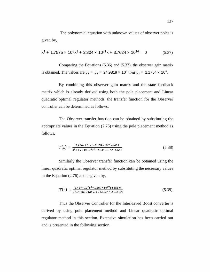
124
CHAPTER 5
DESIGN, MODELLING AND IMPLEMENTATION
OF INTERLEAVED BOOST CONVERTER WITH
OBSERVER CONTROLLER
5.1 OVERVIEW
This chapter discusses in detail about the design and modelling of the Interleaved Boost converter with the Observer controller. The derivation of the state feedback gain matrix using pole placement method and Linear quadratic optimal regulator method are explained. The derivation of the full order state observer and the observer controller are also explained in detail. The simulation results are presented and discussed. The first section explains the design and state space modelling of the Interleaved Boost converter.
5.2 DESIGN AND MODELLING OF INTERLEAVED BOOST CONVERTER
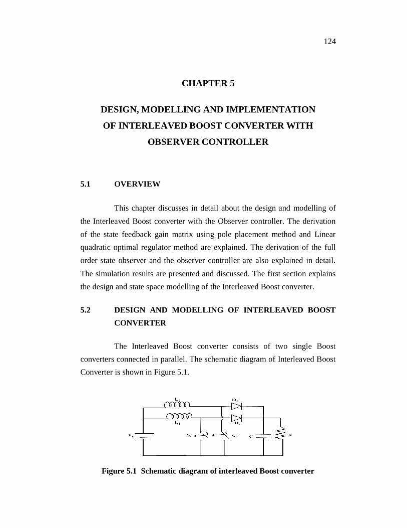
The Interleaved Boost converter consists of two single Boost converters connected in parallel. The schematic diagram of Interleaved Boost Converter is shown in Figure 5.1.
Figure 5.1 Schematic diagram of interleaved Boost converter
125
Here Vs is the input voltage, L1 and L2 are the magnetizing
inductances, S1 and S2 are semiconductor switches, D1 and D2 are diodes, C is
an output capacitor and R is a load resistance respectively. The design
involves the selection of inductors and output capacitor. In interleaved design
both the inductors must be identical. In particular, the design assumes the
room temperature operation over the entire input voltage without the air flow
requirement. Major design of the converter involves the selection of inductor
which is discussed now.
Inductor value can be calculated by assuming peak to peak inductor
ripple to a certain percentage of about 20% of the output current
corresponding to the individual phase. The average inductor current is
determined as,
( ) = . × (5.1)
where Iout is the load current and Dmax is the maximum duty cycle ratio and it
is defined as,
= ( ) (5.2)
where Vout is the output voltage, Vd is the forward diode voltage drop, Von is
the on stage voltage of the MOSFET and Vin (min) is the minimum input
voltage.
Assuming peak inductor ripple current per phase ( IL) as 20% of
the average inductor current, the peak inductor current is determined as
follows,
= ( ) + (5.3)
126
Assuming appropriate switching frequency, the inductor value is
selected using the following equation,
= ( ) ( )(5.4)
Knowing the minimum load current, L value can be designed which
gives the critical value to maintain the converter in continuous mode of
operation.
By assuming appropriate peak to peak capacitor ripple, the output
capacitor value can be obtained using the following equation,
= ( ) ( )(5.5)
where Dmin is the minimum duty cycle defined as,
= ( ) (5.6)
Based on the above discussion the parameters designed for
Interleaved Boost Converter is shown in Table 5.1.
Table 5.1 Design values of interleaved Boost converter
Sl.No Parameters Design Values
1 Input Voltage 24 V
2 Output Voltage 50 V
3 Inductance, L1=L2 72 µH
4 Capacitance, C 216.9X10⁻⁶ F
5 Load Resistance, R 23
6 Switching frequency, fs 20 kHz
127
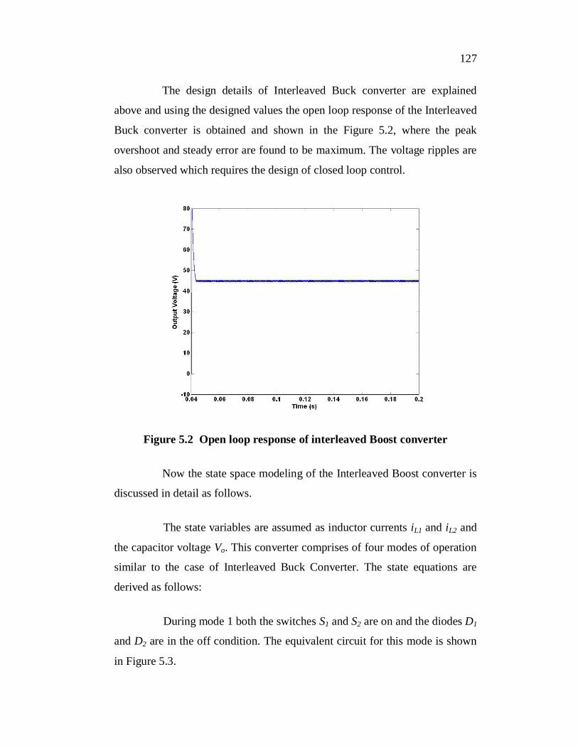
The design details of Interleaved Buck converter are explained
above and using the designed values the open loop response of the Interleaved
Buck converter is obtained and shown in the Figure 5.2, where the peak
overshoot and steady error are found to be maximum. The voltage ripples are
also observed which requires the design of closed loop control.
Figure 5.2 Open loop response of interleaved Boost converter
Now the state space modeling of the Interleaved Boost converter is
discussed in detail as follows.
The state variables are assumed as inductor currents iL1 and iL2 and
the capacitor voltage Vo. This converter comprises of four modes of operation
similar to the case of Interleaved Buck Converter. The state equations are
derived as follows:
During mode 1 both the switches S1 and S2 are on and the diodes D1
and D2 are in the off condition. The equivalent circuit for this mode is shown
in Figure 5.3.
128
Figure 5.3 Equivalent circuit of interleaved Boost converter for mode 1
Applying Kirchoff’s laws to the above circuit, the equations
describing this converter for mode 1 can be obtained as follows,
= (5.7)
= (5.8)
= (5.9)
The coefficient matrices for this mode can be written as,
=0 0 00 0 00 0
(5.10)
and
0
(5.11)
129
During mode 2, the switch S1 is in on condition and switch S2 is in
off condition and the corresponding diodes are in the complementary
switching states, (i.e.) D1 is in off condition and D2 is in on condition
respectively. The equivalent circuit for this mode is shown in Figure 5.4.
Figure 5.4 Equivalent circuit of interleaved Boost converter for mode 2
Applying Kirchoff’s laws to the above circuit, the equations
describing this converter for mode 2 can be obtained as follows,
= (5.12)
= (5.13)
= (5.14)
The coefficient matrices for this mode can be written as,
0 0 00 0
0 (5.15)
130
and
0
(5.16)
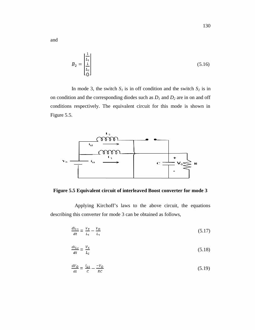
In mode 3, the switch S1 is in off condition and the switch S2 is in
on condition and the corresponding diodes such as D1 and D2 are in on and off
conditions respectively. The equivalent circuit for this mode is shown in
Figure 5.5.
Figure 5.5 Equivalent circuit of interleaved Boost converter for mode 3
Applying Kirchoff’s laws to the above circuit, the equations
describing this converter for mode 3 can be obtained as follows,
= (5.17)
= (5.18)
= (5.19)
131
The coefficient matrices for this mode can be written as,
0 00 0 0
0 (5.20)
and
0
(5.21)
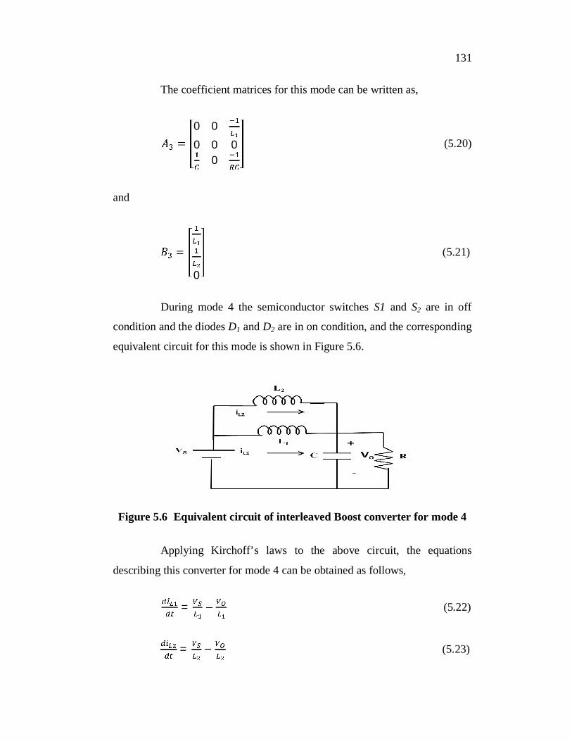
During mode 4 the semiconductor switches S1 and S2 are in off
condition and the diodes D1 and D2 are in on condition, and the corresponding
equivalent circuit for this mode is shown in Figure 5.6.
Figure 5.6 Equivalent circuit of interleaved Boost converter for mode 4
Applying Kirchoff’s laws to the above circuit, the equations
describing this converter for mode 4 can be obtained as follows,
= (5.22)
= (5.23)
132
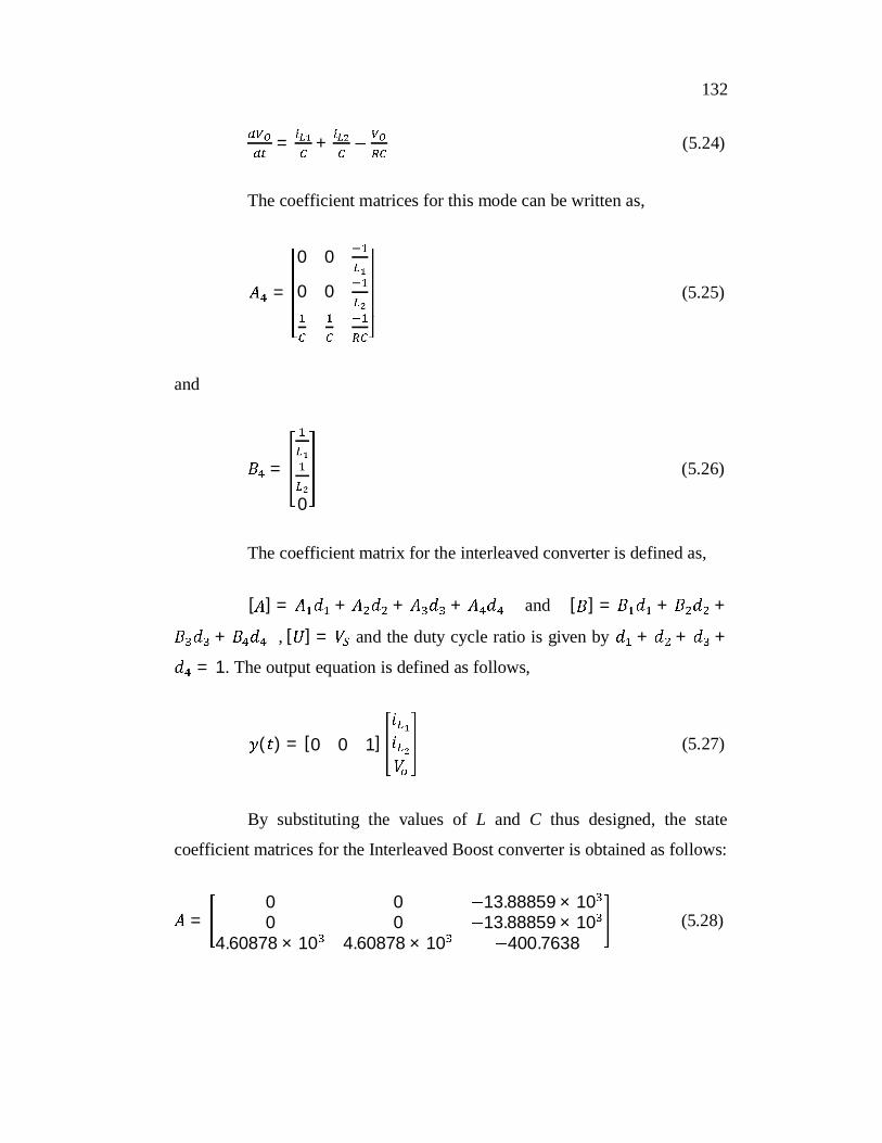
= + (5.24)
The coefficient matrices for this mode can be written as,
=
0 0
0 0 (5.25)
and
=
0
(5.26)
The coefficient matrix for the interleaved converter is defined as,
[ ] = + + + and [ ] = + +
+ , [ ] = and the duty cycle ratio is given by + + +
= 1. The output equation is defined as follows,
( ) = [0 0 1] (5.27)
By substituting the values of L and C thus designed, the state
coefficient matrices for the Interleaved Boost converter is obtained as follows:
=0 0 13.88859 × 100 0 13.88859 × 10
4.60878 × 10 4.60878 × 10 400.7638 (5.28)
133
=27.77733 × 1027.77733 × 10
0 (5.29)
= [0 0 1] (5.30)
= [0] (5.31)
Thus the design and the state space modelling of the Interleaved
Boost converter is explained above section and the detailed discussion about
the derivation of the Observer controller for this converter is explained in the
following section. Similar to the Interleaved Buck converter, the state
feedback matrix for this converter is also derived using both the pole
placement method and Linear Quadratic optimal regulator method. Finally the
above matrix derived using both the methods are combined together with the
observer gain matrix using Separation principle to obtain two different
transfer functions which are explained in detail in the following sections.
5.3 DERIVATION OF STATE FEEDBACK MATRIX FOR
INTERLEAVED BOOST CONVERTER
5.3.1 Pole Placement Method
In this section the state feedback matrix for the Interleaved Boost
converter using pole placement method is derived. The procedure for the
design is same as that used for the other converters which have already been
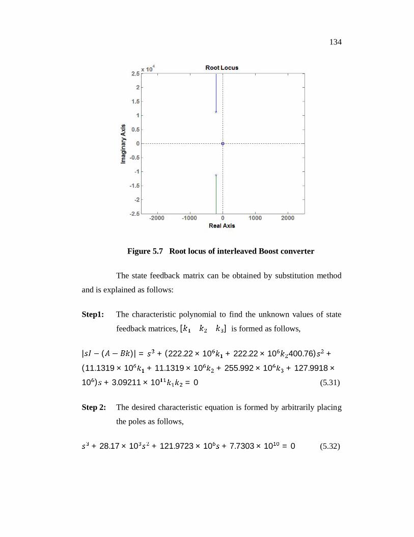
explained in the previous chapters. The root locus of the Interleaved Boost
converter is drawn as shown in the Figure 5.7. The desired poles are
arbitrarily placed in order to obtain the state feedback matrix.
134
Figure 5.7 Root locus of interleaved Boost converter
The state feedback matrix can be obtained by substitution method
and is explained as follows:
Step1: The characteristic polynomial to find the unknown values of state