Chapter 5 The Processor: Datapath and Control Basic MIPS Architecture Homework 2 due October 28 th . Project Designs due October 28 th . Project Reports due November 6 th . Names on Breadboards? Midterm ? Scheduled for Thursday?
Transcript
Chapter 5
The Processor: Datapath and Control
Basic MIPS Architecture
Homework 2 due October 28th.
Project Designs due October 28th.
Project Reports due November 6th.
Names on Breadboards?
Midterm ? Scheduled for Thursday?
Home Work 3 (due Nov 4)
1) Problems 5.8
2) Problem 5.30
Show the progressions and control signals through the multicycle datapath with:
3) An lw instruction
4) An add instruction
5) A beq instruction
Performance Equation (see Chapter 4) A basic performance equation is:
CPU time = Instruction_count x CPI x clock_cycle_time
Instruction_count x CPI
clock_rate CPU time = ----------------------------------------
or
The equations identify three key factors that affect performance
The clock rate (Clock cycle time) is available in the documentation
Instruction count can be measured by using profilers/simulators without knowing all of the implementation details
CPI varies(?) by instruction type and ISA implementation for which we must know the implementation details
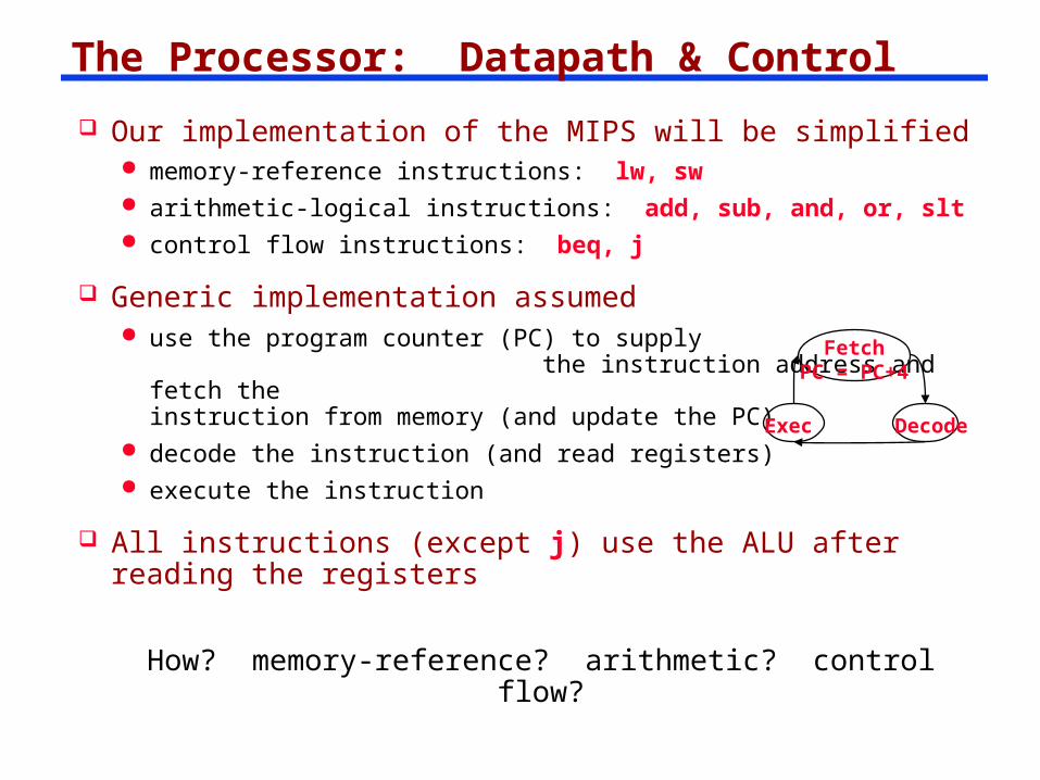
Our implementation of the MIPS will be simplified memory-reference instructions: lw, sw arithmetic-logical instructions: add, sub, and, or, slt control flow instructions: beq, j
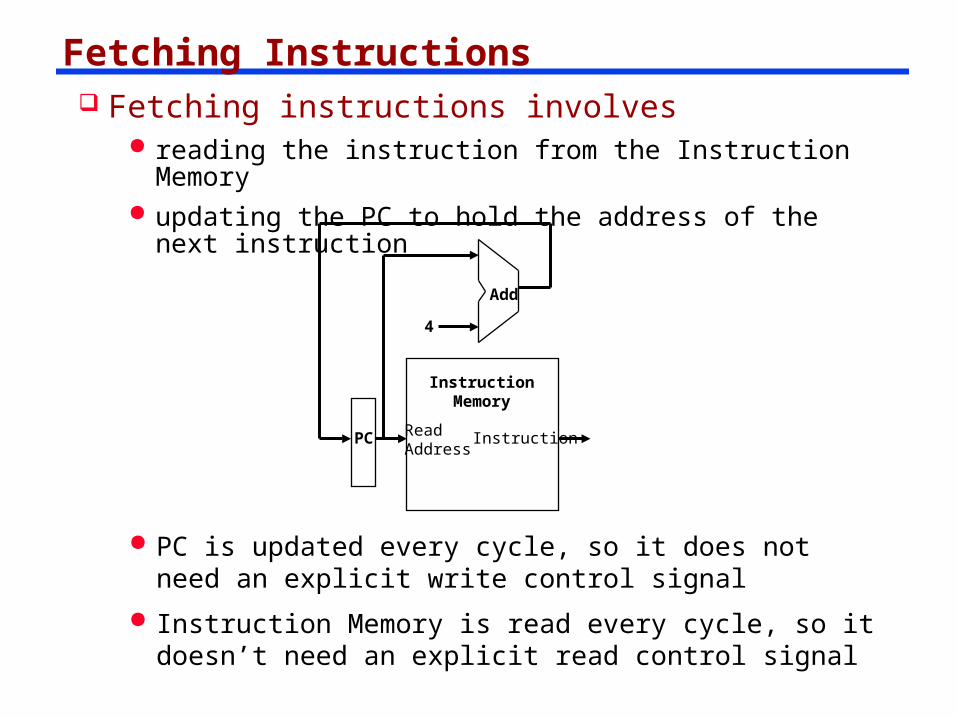
Generic implementation assumed use the program counter (PC) to supply
the instruction address and fetch the instruction from memory (and update the PC)
decode the instruction (and read registers) execute the instruction
All instructions (except j) use the ALU after reading the registers
How? memory-reference? arithmetic? control flow?
The Processor: Datapath & Control
FetchPC = PC+4
DecodeExec
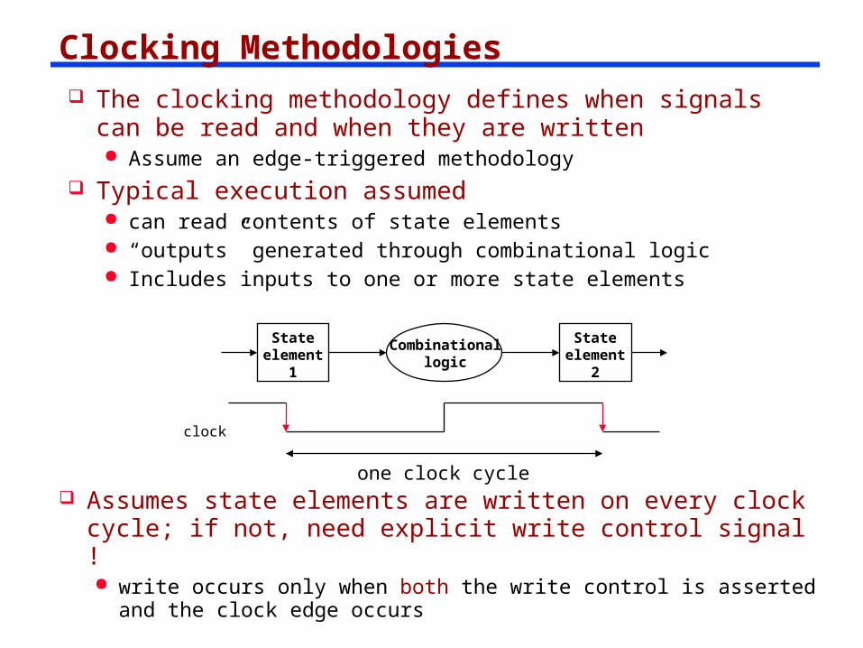
Clocking Methodologies The clocking methodology defines when signals
can be read and when they are written Assume an edge-triggered methodology
Typical execution assumed can read contents of state elements “outputs” generated through combinational logic Includes inputs to one or more state elements
Stateelement
1
Stateelement
2
Combinationallogic
clock
one clock cycle Assumes state elements are written on every clock
cycle; if not, need explicit write control signal ! write occurs only when both the write control is asserted and
the clock edge occurs
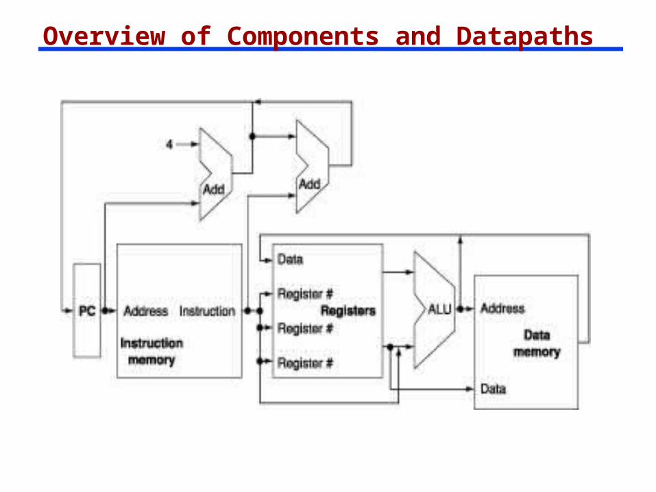
Overview of Components and Datapaths
Creating a Single Datapath from the Parts Assemble the datapath segments and add
control lines and multiplexors as needed Single cycle design – fetch, decode and execute
each instructions in one clock cycle no datapath resource can be used more than once per
instruction, so some must be duplicated (e.g., separate Instruction Memory and Data Memory, several adders)
multiplexors needed at the input of shared elements with control lines to do the selection
write signals to control writing to the Register File and Data Memory
Cycle time is determined by length of the longest path
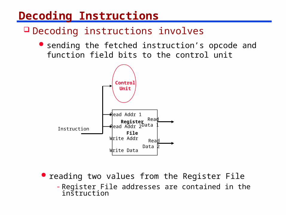
sending the fetched instruction’s opcode and function field bits to the control unit
Instruction
Write Data
Read Addr 1
Read Addr 2
Write Addr
Register
File
Read Data 1
Read Data 2
ControlUnit
reading two values from the Register File- Register File addresses are contained in the instruction
Executing R Format Operations R format operations (add, sub, slt, and, or)
perform the (op and funct) operation on values in rs and rt store the result back into the Register File (into location
rd)
Instruction
Write Data
Read Addr 1
Read Addr 2
Write Addr
Register
File
Read Data 1
Read Data 2
ALU
overflowzero
ALU controlRegWrite
R-type:
31 25 20 15 5 0
op rs rt rd functshamt
10
The Register File is not written every cycle (e.g. sw), so we need an explicit write control signal for the Register File
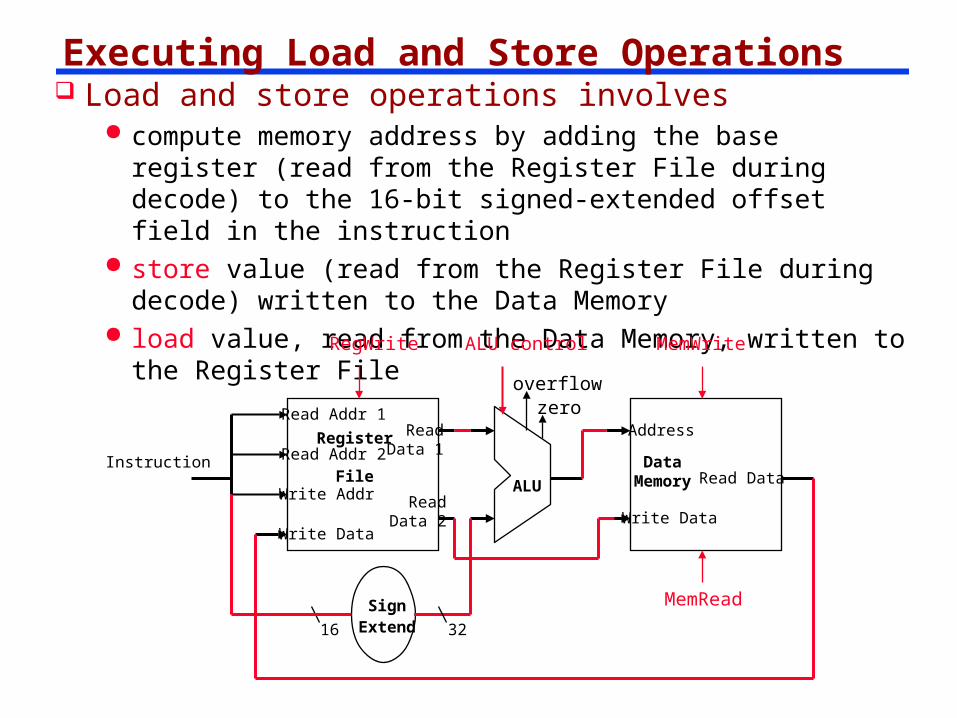
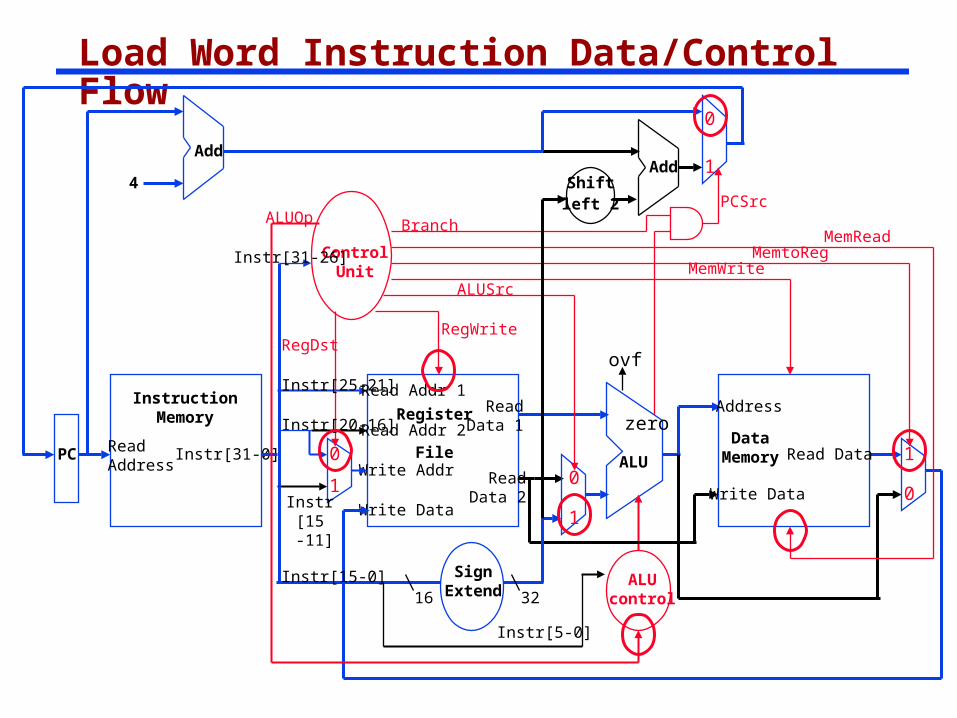
Executing Load and Store Operations Load and store operations involves
compute memory address by adding the base register (read from the Register File during decode) to the 16-bit signed-extended offset field in the instruction
store value (read from the Register File during decode) written to the Data Memory
load value, read from the Data Memory, written to the Register File
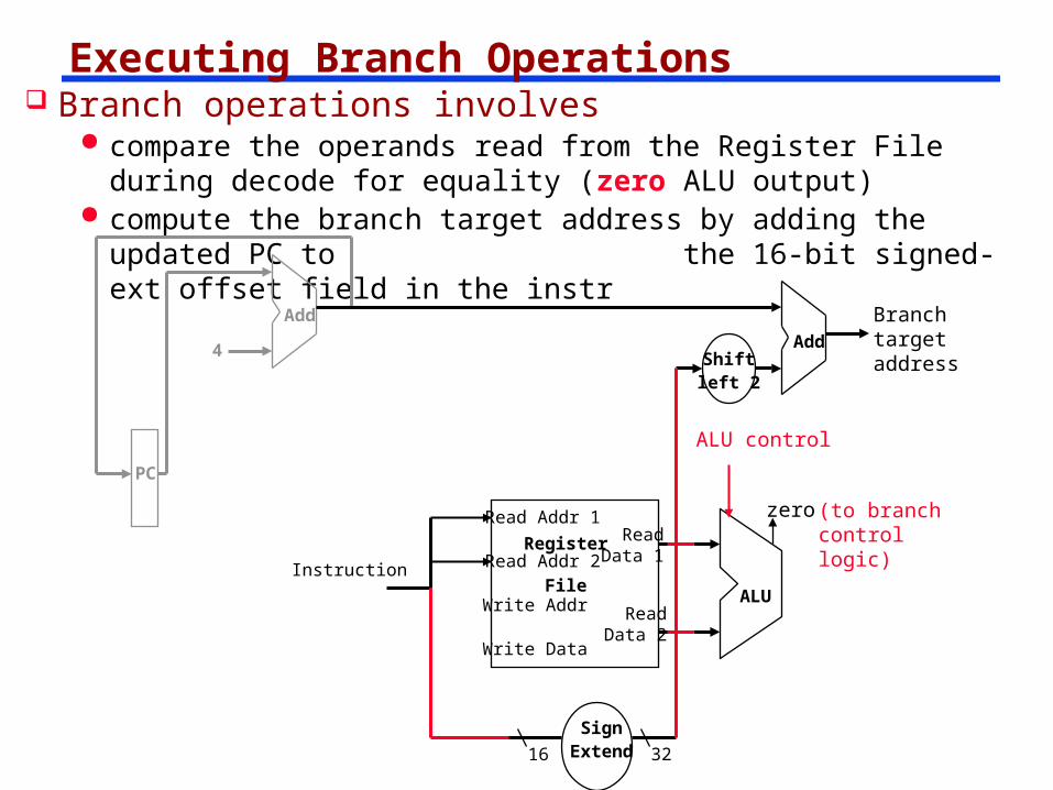
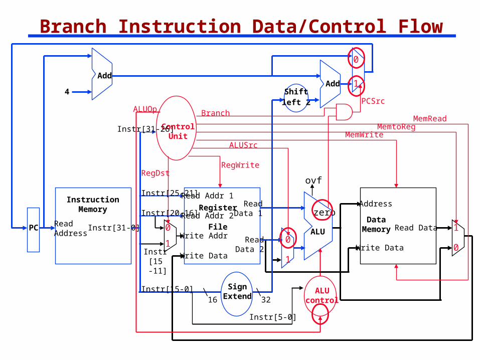
compare the operands read from the Register File during decode for equality (zero ALU output)
compute the branch target address by adding the updated PC to the 16-bit signed-ext offset field in the instr
Instruction
Write Data
Read Addr 1
Read Addr 2
Write Addr
Register
File
Read Data 1
Read Data 2
ALU
zero
ALU control
SignExtend16 32
Shiftleft 2
Add
4 Add
PC
Branchtargetaddress
(to branch control logic)
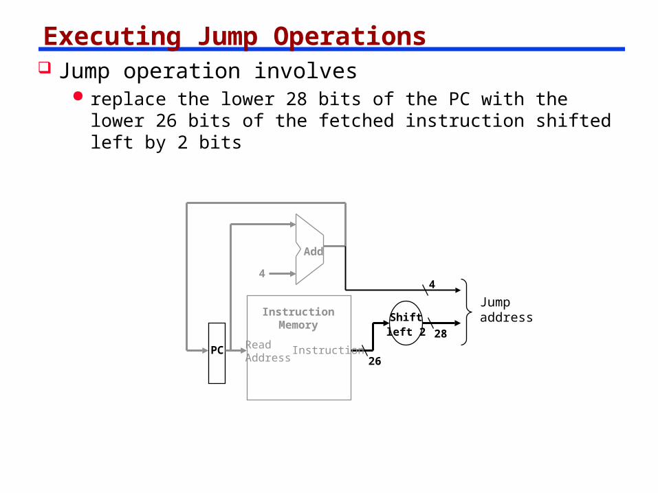
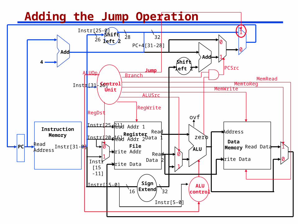
Executing Jump Operations Jump operation involves
replace the lower 28 bits of the PC with the lower 26 bits of the fetched instruction shifted left by 2 bits
ReadAddress
Instruction
InstructionMemory
Add
PC
4
Shiftleft 2
Jumpaddress
26
4
28
Fetch, R, and Memory Access Portions
MemtoReg
ReadAddress
Instruction
InstructionMemory
Add
PC
4
Write Data
Read Addr 1
Read Addr 2
Write Addr
Register
File
Read Data 1
Read Data 2
ALU
ovfzero
ALU controlRegWrite
DataMemory
Address
Write Data
Read Data
MemWrite
MemReadSign
Extend16 32
ALUSrc
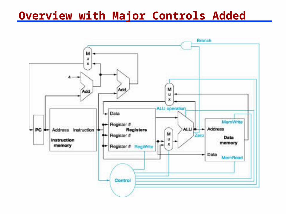
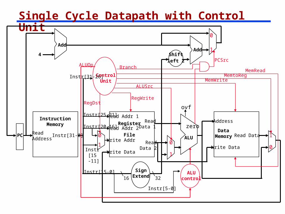
Adding the Control Selecting the operations to perform (ALU, Register
File and Memory read/write) Controlling the flow of data (multiplexor inputs)
I-Type: op rs rt address offset
31 25 20 15 0
R-type:
31 25 20 15 5 0
op rs rt rd functshamt
10
Observations op field always
in bits 31-26
addr of registers to be read are always specified by the rs field (bits 25-21) and rt field (bits 20-16); for lw and sw rs is the base register
addr. of register to be written is in one of two places – in rt (bits 20-16) for lw; in rd (bits 15-11) for R-type instructions
offset for beq, lw, and sw always in bits 15-0
J-type:31 25 0
op target address
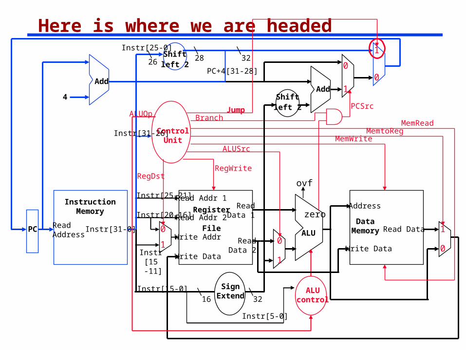
Single Cycle Datapath with Control Unit
ReadAddress
Instr[31-0]
InstructionMemory
Add
PC
4
Write Data
Read Addr 1
Read Addr 2
Write Addr
Register
File
Read Data 1
Read Data 2
ALU
ovf
zero
RegWrite
DataMemory
Address
Write Data
Read Data
MemWrite
MemRead
SignExtend16 32
MemtoReg
ALUSrc
Shiftleft 2
Add
PCSrc
RegDst
ALUcontrol
1
1
1
00
0
0
1
ALUOp
Instr[5-0]
Instr[15-0]
Instr[25-21]
Instr[20-16]
Instr[15 -11]
ControlUnit
Instr[31-26]
Branch
R-type Instruction Data/Control Flow
ReadAddress
Instr[31-0]
InstructionMemory
Add
PC
4
Write Data
Read Addr 1Read Addr 2
Write Addr
Register
File
Read Data 1
Read Data 2
ALU
ovf
zero
RegWrite
DataMemory
Address
Write Data
Read Data
MemWrite
MemRead
SignExtend16 32
MemtoReg
ALUSrc
Shiftleft 2
Add
PCSrc
RegDst
ALUcontrol
1
1
1
00
0
0
1
ALUOp
Instr[5-0]
Instr[15-0]
Instr[25-21]
Instr[20-16]
Instr[15 -11]
ControlUnit
Instr[31-26]
Branch
Load Word Instruction Data/Control Flow
ReadAddress
Instr[31-0]
InstructionMemory
Add
PC
4
Write Data
Read Addr 1
Read Addr 2
Write Addr
Register
File
Read Data 1
Read Data 2
ALU
ovf
zero
RegWrite
DataMemory
Address
Write Data
Read Data
MemWrite
MemRead
SignExtend16 32
MemtoReg
ALUSrc
Shiftleft 2
Add
PCSrc
RegDst
ALUcontrol
1
1
1
00
0
0
1
ALUOp
Instr[5-0]
Instr[15-0]
Instr[25-21]
Instr[20-16]
Instr[15 -11]
ControlUnit
Instr[31-26]
Branch
Branch Instruction Data/Control Flow
ReadAddress
Instr[31-0]
InstructionMemory
Add
PC
4
Write Data
Read Addr 1
Read Addr 2
Write Addr
Register
File
Read Data 1
Read Data 2
ALU
ovf
zero
RegWrite
DataMemory
Address
Write Data
Read Data
MemWrite
MemRead
SignExtend16 32
MemtoReg
ALUSrc
Shiftleft 2
Add
PCSrc
RegDst
ALUcontrol
1
1
1
00
0
0
1
ALUOp
Instr[5-0]
Instr[15-0]
Instr[25-21]
Instr[20-16]
Instr[15 -11]
ControlUnit
Instr[31-26]
Branch
Adding the Jump Operation
ReadAddress
Instr[31-0]
InstructionMemory
Add
PC
4
Write Data
Read Addr 1
Read Addr 2
Write Addr
Register
File
Read Data 1
Read Data 2
ALU
ovf
zero
RegWrite
DataMemory
Address
Write Data
Read Data
MemWrite
MemRead
SignExtend16 32
MemtoReg
ALUSrc
Shiftleft 2
Add
PCSrc
RegDst
ALUcontrol
1
1
1
00
0
0
1
ALUOp
Instr[5-0]
Instr[15-0]
Instr[25-21]
Instr[20-16]
Instr[15 -11]
ControlUnit
Instr[31-26]
Branch
Shiftleft 2
0
1
Jump
32Instr[25-0]
26PC+4[31-28]
28
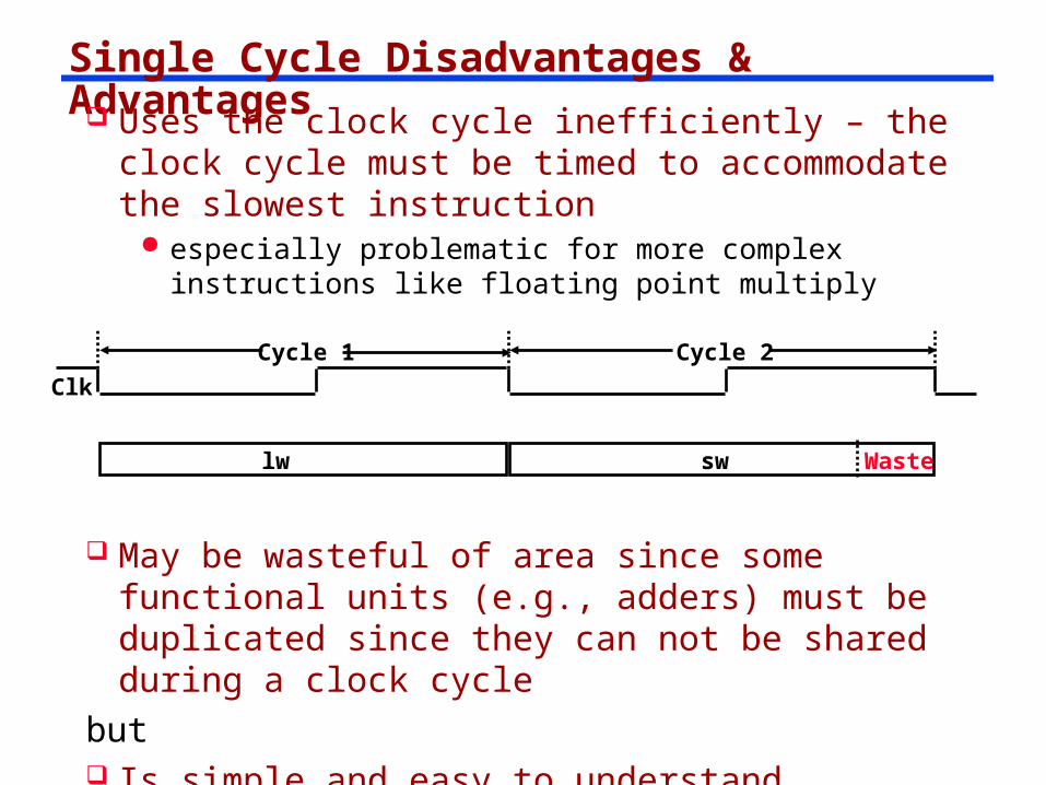
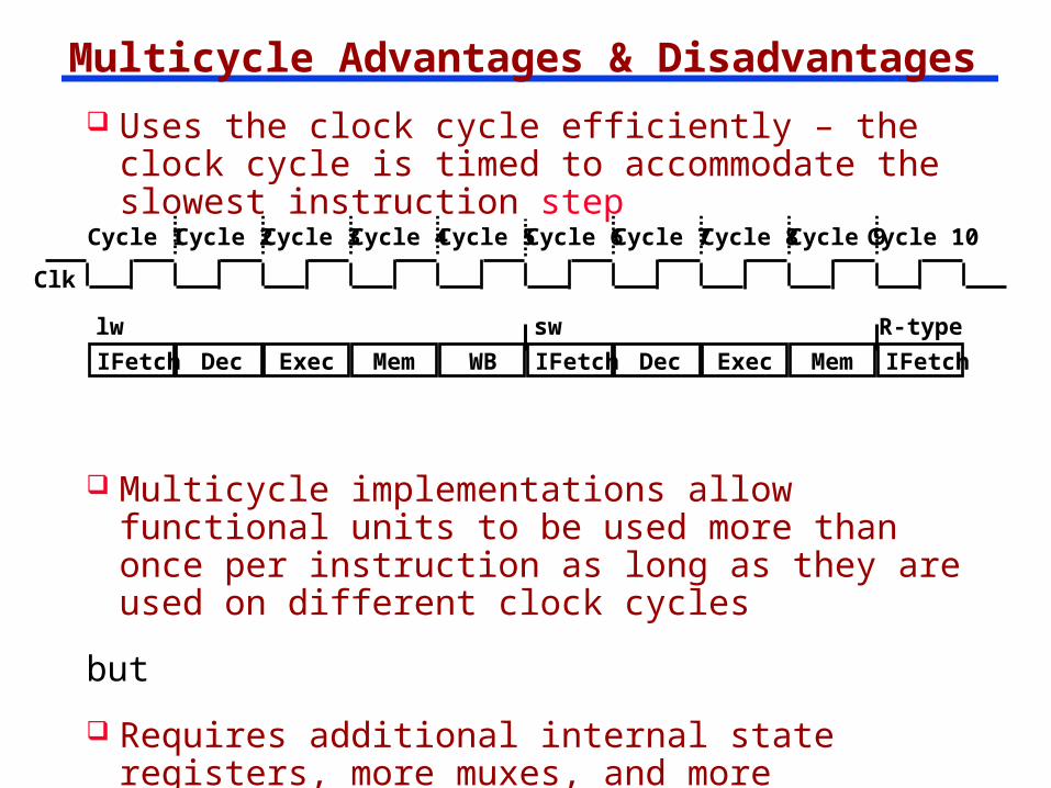
Single Cycle Disadvantages & Advantages Uses the clock cycle inefficiently – the clock
cycle must be timed to accommodate the slowest instruction
especially problematic for more complex instructions like floating point multiply
May be wasteful of area since some functional units (e.g., adders) must be duplicated since they can not be shared during a clock cycle
but Is simple and easy to understand
Clk
lw sw Waste
Cycle 1 Cycle 2
Multicycle Datapath
Implementation
More complex but allows significant performance increase
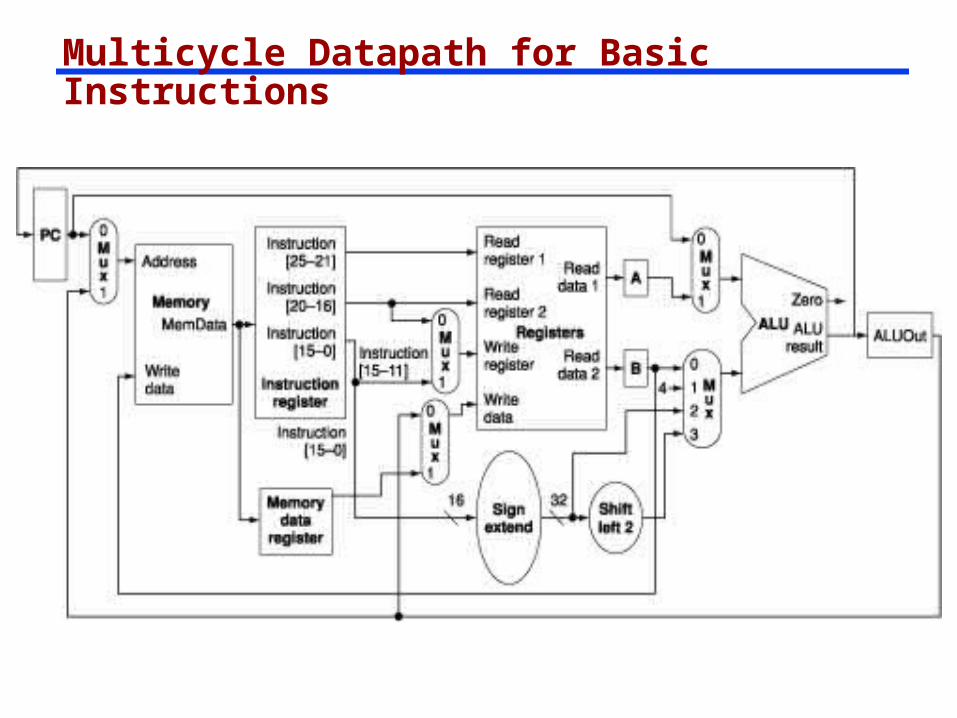
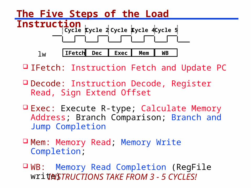
Multicycle Datapath Approach Let an instruction take more than 1 clock cycle to
complete Not every instruction takes the same number of clock
cycles Break up instructions into steps where each step takes a
cycle while trying to- balance the amount of work to be done in each step
- restrict each cycle to use only one major functional unit
In addition to faster clock rates, multicycle allows functional units that can be used more than once per instruction as long as they are used on different clock cycles, as a result
only need one memory – but only one memory access per cycle
need only one ALU/adder – but only one ALU operation per cycle
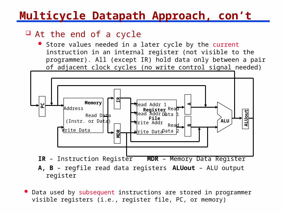
At the end of a cycle Store values needed in a later cycle by the current instruction in
an internal register (not visible to the programmer). All (except IR) hold data only between a pair of adjacent clock cycles (no write control signal needed)
IR – Instruction Register MDR – Memory Data RegisterA, B – regfile read data registers ALUout – ALU output register
Multicycle Datapath Approach, con’t
Address
Read Data(Instr. or Data)
Memory
PC
Write Data
Read Addr 1
Read Addr 2
Write Addr
Register
File
Read Data 1
Read Data 2
ALU
Write Data
IRM
DR
AB A
LU
ou
t
Data used by subsequent instructions are stored in programmer visible registers (i.e., register file, PC, or memory)
Multicycle Datapath for Basic Instructions
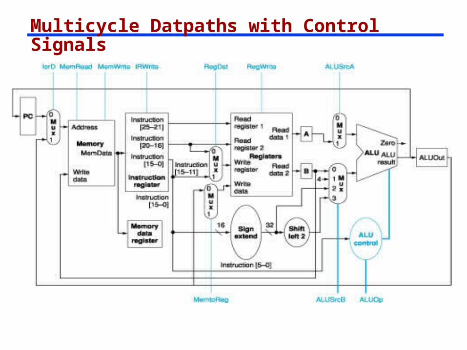
Multicycle Datpaths with Control Signals
The Multicycle Datapath with Control Signals
Address
Read Data(Instr. or Data)
Memory
PC
Write Data
Read Addr 1
Read Addr 2
Write Addr
Register
File
Read Data 1
Read Data 2
ALU
Write Data
IRM
DR
AB
AL
Uo
ut
SignExtend
Shiftleft 2 ALU
control
Shiftleft 2
ALUOpControl
IRWriteMemtoReg
MemWriteMemRead
IorD
PCWrite
PCWriteCond
RegDstRegWrite
ALUSrcAALUSrcB
zero
PCSource
1
1
1
1
1
10
0
0
0
0
0
2
2
3
4
Instr[5-0]
Instr[25-0]
PC[31-28]
Instr[15-0]
Instr[3
1-2
6]
32
28
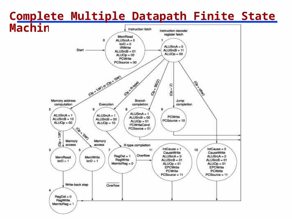
Complete Multiple Datapath Finite State Machine
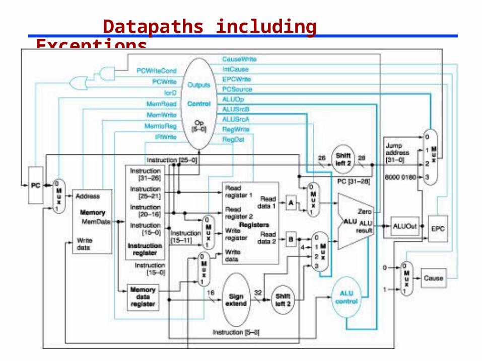
Exception Considerations
Exceptions like overflow, memory partition violation, and invalid instruction
- “Cause” register – a bit for each possible exception
- Data register – a register with pertinent information
- Transfer to Supervisor “Entry Point”
Exceptions system similar to Servicing Events and Devices
- Vector System (Pointers to service routines)- Load Vector and transfer- May have a priority & arbitration system
Datapaths including Exceptions
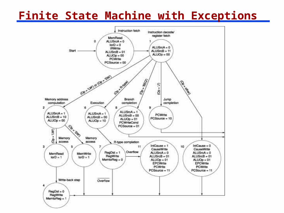
Finite State Machine with Exceptions
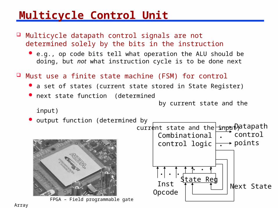
Multicycle datapath control signals are not determined solely by the bits in the instruction e.g., op code bits tell what operation the ALU should be
doing, but not what instruction cycle is to be done next
Must use a finite state machine (FSM) for control a set of states (current state stored in State Register) next state function (determined
by current state and the input) output function (determined by