Page 1
Copyright © 2017 McGraw-Hill Education. All rights reserved. No reproduction or distribution without the prior written consent of McGraw-Hill Education.
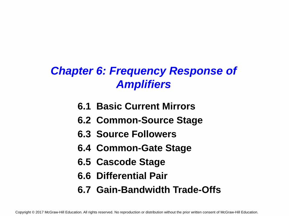
Chapter 6: Frequency Response of Amplifiers
6.1 Basic Current Mirrors
6.2 Common-Source Stage
6.3 Source Followers
6.4 Common-Gate Stage
6.5 Cascode Stage
6.6 Differential Pair
6.7 Gain-Bandwidth Trade-Offs
Page 2
Copyright © 2017 McGraw-Hill Education. All rights reserved. No reproduction or distribution without the prior written consent of McGraw-Hill Education. 2
General Considerations
• In this chapter, we are primarily interested in the magnitude of the transfer function.
• The magnitude of a complex number a + jb is given by .
• Zeros and poles are respectively defined as the roots of the numerator and denominator of the transfer function.
Page 3
Copyright © 2017 McGraw-Hill Education. All rights reserved. No reproduction or distribution without the prior written consent of McGraw-Hill Education. 3
Miller effect
• If the circuit of Fig (a) can be converted to that of Fig (b), then
Page 4
Copyright © 2017 McGraw-Hill Education. All rights reserved. No reproduction or distribution without the prior written consent of McGraw-Hill Education. 4
Example
• A student needs a large Capacitor and decides to utilize the Miller multiplication
• What is the issues in this approach?
Page 5
Copyright © 2017 McGraw-Hill Education. All rights reserved. No reproduction or distribution without the prior written consent of McGraw-Hill Education. 5
• Miller’s theorem does not stipulate the conditions under which this conversion is valid.
• If the impedance Z forms the only signal path between X and Y , then the conversion is often invalid.
Page 6
Copyright © 2017 McGraw-Hill Education. All rights reserved. No reproduction or distribution without the prior written consent of McGraw-Hill Education. 6
Example
• Calculate the input resistance of the circuit shown.
• Since Av is usually greater than unity, is a negative resistance.
• Av =
Page 7
Copyright © 2017 McGraw-Hill Education. All rights reserved. No reproduction or distribution without the prior written consent of McGraw-Hill Education. 7
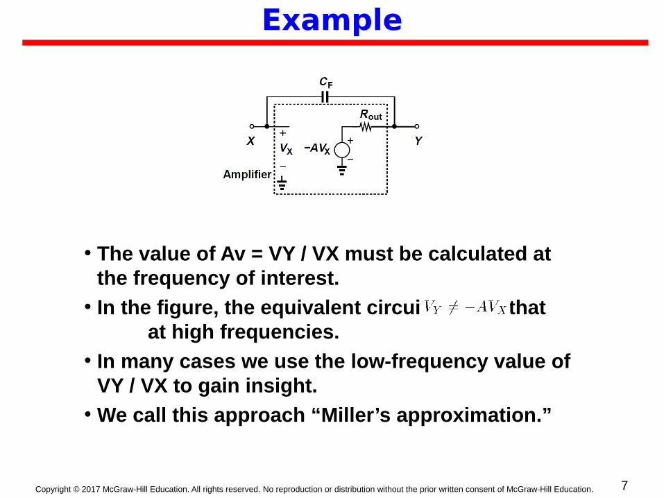
Example
• The value of Av = VY / VX must be calculated at the frequency of interest.
• In the figure, the equivalent circuit reveals that at high frequencies.
• In many cases we use the low-frequency value of VY / VX to gain insight.
• We call this approach “Miller’s approximation.”
Page 8
Copyright © 2017 McGraw-Hill Education. All rights reserved. No reproduction or distribution without the prior written consent of McGraw-Hill Education. 8
Example
• Direct Calculation:
• Miller Aproximation:
• Miller’s approximation has eliminated the zero and predicted two poles for the circuit!
Page 9
Copyright © 2017 McGraw-Hill Education. All rights reserved. No reproduction or distribution without the prior written consent of McGraw-Hill Education. 9
Example
• Actual Rout =r0
• Miller’s approximation:
• (1) it may eliminate zeros
• (2) it may predict additional poles
• (3) it does not correctly compute the “output” impedance.
Page 10
Copyright © 2017 McGraw-Hill Education. All rights reserved. No reproduction or distribution without the prior written consent of McGraw-Hill Education. 10
Association of Poles with Nodes
• The overall transfer function can be written as
• Each node in the circuit contributes one pole to the transfer function.
• Not valid in general. Example:
Page 11
Copyright © 2017 McGraw-Hill Education. All rights reserved. No reproduction or distribution without the prior written consent of McGraw-Hill Education. 11
Example
• At node X:
• At node Y:
• The overall transfer funtion:
Page 12
Copyright © 2017 McGraw-Hill Education. All rights reserved. No reproduction or distribution without the prior written consent of McGraw-Hill Education. 12
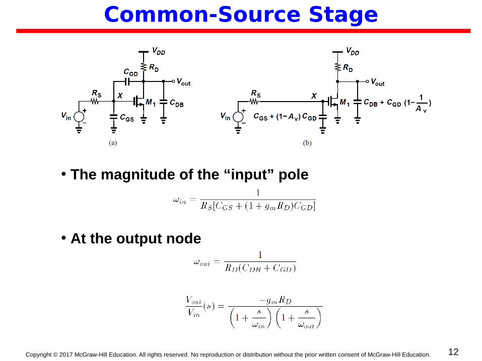
Common-Source Stage
• The magnitude of the “input” pole
• At the output node
Page 13
Copyright © 2017 McGraw-Hill Education. All rights reserved. No reproduction or distribution without the prior written consent of McGraw-Hill Education. 13
Direct Analysis
• While the denominator appears rather complicated, it can yield intuitive expressions for the two poles.
• “Dominant pole” approximation.
• The intuitive approach provides a rough estimate with much less effort.
Page 14
Copyright © 2017 McGraw-Hill Education. All rights reserved. No reproduction or distribution without the prior written consent of McGraw-Hill Education. 14
Example
• One pole is at the origin because the dc gain is infinity.
• For a large CDB or load capacitance
• No miller multiplication. Why?
Page 15
Copyright © 2017 McGraw-Hill Education. All rights reserved. No reproduction or distribution without the prior written consent of McGraw-Hill Education. 15
Zero in Transfer Function
• The transfer function of exhibits a zero given by
• CGD provides a feedthrough path that conducts the input signal to the output at very high frequencies.
Page 16
Copyright © 2017 McGraw-Hill Education. All rights reserved. No reproduction or distribution without the prior written consent of McGraw-Hill Education. 16
Calculating zero in a CS stage
• The transfer function Vout(s)=Vin(s) must drop to zero for s = sz.
• Therefore, the currents through CGD and M1 are equal and opposite:
• That is
Page 17
Copyright © 2017 McGraw-Hill Education. All rights reserved. No reproduction or distribution without the prior written consent of McGraw-Hill Education. 17
Example
• Can this (the zero) occur if H1(s) and H2(s) are first-order low-pass circuits?
• H1= and H2=
• The overall transfer function contains a zero.
Page 18
Copyright © 2017 McGraw-Hill Education. All rights reserved. No reproduction or distribution without the prior written consent of McGraw-Hill Education. 18
Example
• Since the corresponding terminals ofM1 and M2 are shorted to one another in the small-signal model, we merge the two transistors.
• The circuit thus has the same transfer function as the simple CS stage.
Page 19
Copyright © 2017 McGraw-Hill Education. All rights reserved. No reproduction or distribution without the prior written consent of McGraw-Hill Education. 19
Miller’s Approximation
• With the aid of Miller’s approximation,
• But at high frequencies, the effect of the output node capacitance must be taken into account.
• Ignore CGS
• if CGD is large, it provides a low impedance path between the gate and drain of M1.
Page 20
Copyright © 2017 McGraw-Hill Education. All rights reserved. No reproduction or distribution without the prior written consent of McGraw-Hill Education. 20
Source Followers
• The strong interaction between nodesX and Y through CGS in makes it difficult to associate a pole with each node.
• Contains a zero in the left half plane. Why?
Page 21
Copyright © 2017 McGraw-Hill Education. All rights reserved. No reproduction or distribution without the prior written consent of McGraw-Hill Education. 21
Example
• Transfer function if CL = 0?
• CGS disappear
• In the absence of channel-length modulation and body effect, the voltage gain from the gate to the source is equal to unity.
Page 22
Copyright © 2017 McGraw-Hill Education. All rights reserved. No reproduction or distribution without the prior written consent of McGraw-Hill Education. 22
Input impedance
• CGD simply shunts the input and can be ignored initially.
• If gmb = 0 and CL = 0, then Zin = ∞
• CGS is entirely bootstrapped by the source follower and draws no current from the input.
• At Low frequency the overall input capacitance is equal to CGD plus a fraction of CGS.
Page 23
Copyright © 2017 McGraw-Hill Education. All rights reserved. No reproduction or distribution without the prior written consent of McGraw-Hill Education. 23
Input Impedance
• At high frequencies,
• A source follower driving a load capacitance exhibits a negative input resistance, possibly causing instability.
Page 24
Copyright © 2017 McGraw-Hill Education. All rights reserved. No reproduction or distribution without the prior written consent of McGraw-Hill Education. 24
Output Impedance
• At low frequency:• At very high frequencies,
• Because CGS shorts the gate and the source.
• Which one of these variations is more realistic?
Page 25
Copyright © 2017 McGraw-Hill Education. All rights reserved. No reproduction or distribution without the prior written consent of McGraw-Hill Education. 25
Output Impedance
• Since the output impedance increases with frequency, we postulate that it contains an inductive component.
Page 26
Copyright © 2017 McGraw-Hill Education. All rights reserved. No reproduction or distribution without the prior written consent of McGraw-Hill Education. 26
Example
• Can we construct a (two-terminal) inductor from a source follower?
• Yes, but non-ideal.
• It also incurs a parallel resistance and a series resistance.
• The inductance can partially cancel the load capacitance, CL, at high frequencies, thus extending the bandwidth.
Page 27
Copyright © 2017 McGraw-Hill Education. All rights reserved. No reproduction or distribution without the prior written consent of McGraw-Hill Education. 27
Common-Gate Stage
• A transfer function
• No Miller multiplication of capacitances.
• RD is typically maximized, so the dc level of the input signal must be quite low.
• As an amplifier in cases where a low input impedance is required
• In cascode stages.
Page 28
Copyright © 2017 McGraw-Hill Education. All rights reserved. No reproduction or distribution without the prior written consent of McGraw-Hill Education. 28
Example
• Why Zin becomes independent of CL as this capacitance increases?
• As CL or s increases, Zin approaches 1/(gm + gmb)
• CL lowers the voltage gain of the circuit, thereby suppressing the effect of the negative resistance introduced by Miller effect through rO.
Page 29
Copyright © 2017 McGraw-Hill Education. All rights reserved. No reproduction or distribution without the prior written consent of McGraw-Hill Education. 29
CG Stage
• The bias network providing the gate voltage exhibits a finite impedance.
• Consider only CGS here.
• Lowering the pole magnitude.
• Output impedance of the circuit drops at high frequencies.
Page 30
Copyright © 2017 McGraw-Hill Education. All rights reserved. No reproduction or distribution without the prior written consent of McGraw-Hill Education. 30
Cascode Stage
• Miller effect is less significant in cascode amplifiers than in common-source stages.
• But I is typically quite higher than the other two.
• What if RD is replaced by a current source?
• Pole at node X may be quite lower, but transfer function will not affect much by this. See example.
Page 31
Copyright © 2017 McGraw-Hill Education. All rights reserved. No reproduction or distribution without the prior written consent of McGraw-Hill Education. 31
Example
• Compute the transfer function.
• For
• The magnitude of the pole at node X is still given by gm2/CX. Why?
Page 32
Copyright © 2017 McGraw-Hill Education. All rights reserved. No reproduction or distribution without the prior written consent of McGraw-Hill Education. 32
Differential Pair
• For differential signals, the response is identical to that of a common-source stage.
• the common-mode rejection of the circuit degrades considerably at high frequencies.
• Channel-length modulation, body effect, and other capacitances are neglected.
Page 33
Copyright © 2017 McGraw-Hill Education. All rights reserved. No reproduction or distribution without the prior written consent of McGraw-Hill Education. 33
Differential Pair
• This transfer function contains a zero and a pole.
• The magnitude of the zero is much greater than the pole.
• Common-mode disturbance at node P translates to a differential noise component at the output, if the supply voltage contains high-frequency noise and the circuit exhibits mismatches.
• Trade-off between voltage headroom and CMRR.
Page 34
Copyright © 2017 McGraw-Hill Education. All rights reserved. No reproduction or distribution without the prior written consent of McGraw-Hill Education. 34
Diff Pair
• Frequency response of differential pairs with high-impedance loads.
• Fig (b) CGD3 and CGD4 conduct equal and opposite currents to node G, making this node an ac ground.
• The differential half circuit is depicted in Fig. (c).
• More on chapter 10
Page 35
Copyright © 2017 McGraw-Hill Education. All rights reserved. No reproduction or distribution without the prior written consent of McGraw-Hill Education. 35
Differential Pair with Active Load
• How many poles does this circuit have?
• The severe trade-off between gm and CGS of PMOS devices results in a pole that impacts the performance of the circuit.
• The pole associated with node E is called a “mirror pole.”
Page 36
Copyright © 2017 McGraw-Hill Education. All rights reserved. No reproduction or distribution without the prior written consent of McGraw-Hill Education. 36
Active Load
• Replacing Vin, M1, and M2 by a Thevenin equivalent.
Page 37
Copyright © 2017 McGraw-Hill Education. All rights reserved. No reproduction or distribution without the prior written consent of McGraw-Hill Education. 37
Active Load
• A zero with a magnitude of in the left half plane.
• The appearance of such a zero can be understood by noting that the circuit consists of a “slow path” (M1,M3 and M4) in parallel with a “fast path” (M1 and M2) by and
Page 38
Copyright © 2017 McGraw-Hill Education. All rights reserved. No reproduction or distribution without the prior written consent of McGraw-Hill Education. 38
Example
• Not all fully differential circuits are free from mirror poles.
• Estimate the low-frequency gain and the transfer function of this circuit.
Page 39
Copyright © 2017 McGraw-Hill Education. All rights reserved. No reproduction or distribution without the prior written consent of McGraw-Hill Education. 39
Example
• M5 multiplies the drain current of M3 by K.
• Assume RDCL is relatively small so that the Miller multiplication of CGD5 can be approximated as
• The overall transfer function is then equal to
Vx/Vin1 multiplied by Vout1/Vx.
Page 40
Copyright © 2017 McGraw-Hill Education. All rights reserved. No reproduction or distribution without the prior written consent of McGraw-Hill Education. 40
Gain-Bandwidth Trade-Offs
• We wish to maximize both the gain and the bandwidth of amplifiers.
• we are interested in both the 3-dB bandwidth, , and the “unity-gain” bandwidth,
Page 41
Copyright © 2017 McGraw-Hill Education. All rights reserved. No reproduction or distribution without the prior written consent of McGraw-Hill Education. 41
One pole circuit
Page 42
Copyright © 2017 McGraw-Hill Education. All rights reserved. No reproduction or distribution without the prior written consent of McGraw-Hill Education. 42
Multi-Pole Circuits
• It is possible to increase the GBW product by cascading two or more gain stages.
• Assume the two stages are identical and neglect other capacitances.
• While raising the GBW product, cascading reduces the bandwidth.
Page 43
Copyright © 2017 McGraw-Hill Education. All rights reserved. No reproduction or distribution without the prior written consent of McGraw-Hill Education. 43
Appendix A: Extra Element Theorem
• Suppose the transfer function of a circuit is known and denoted by H(s). Add an extra impedance Z1 between two nodes of the circuit.
• New transfer function:
• Particularly useful for frequency response analysis.
Page 44
Copyright © 2017 McGraw-Hill Education. All rights reserved. No reproduction or distribution without the prior written consent of McGraw-Hill Education. 44
Example 1
• Find the transfer function.
• The negative sign of Zout,0 does not imply a negative impedance between A and B, since
Page 45
Copyright © 2017 McGraw-Hill Education. All rights reserved. No reproduction or distribution without the prior written consent of McGraw-Hill Education. 45
Example 2
• Include CB, from node B to ground.
Page 46
Copyright © 2017 McGraw-Hill Education. All rights reserved. No reproduction or distribution without the prior written consent of McGraw-Hill Education. 46
Appendix B: Zero-Value Time Constant
• Suppose a circuit contains one capacitor and no other storage elements.
• Wish to determine the pole of the system.
• Set the input to zero, compute the resistance, R1, seen by C1, and express the pole as 1/(R1C1).
Page 47
Copyright © 2017 McGraw-Hill Education. All rights reserved. No reproduction or distribution without the prior written consent of McGraw-Hill Education. 47
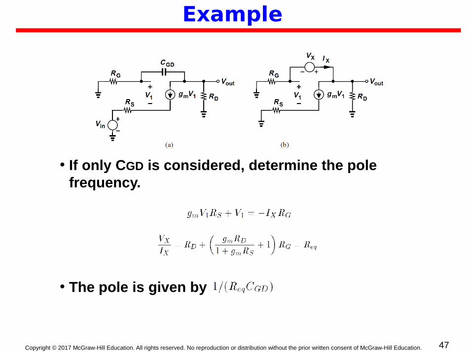
Example
• If only CGD is considered, determine the pole frequency.
• The pole is given by
Page 48
Copyright © 2017 McGraw-Hill Education. All rights reserved. No reproduction or distribution without the prior written consent of McGraw-Hill Education. 48
Example
• Writing a KVL around Vin, R1, R2, and Vout gives
• The dominant pole is indeed equal to the inverse of the sum of the zero-value time constants. (need to prove)
• The ZVTC method proves useful if we wish to estimate the 3-dB bandwidth of a circuit.
Page 49
Copyright © 2017 McGraw-Hill Education. All rights reserved. No reproduction or distribution without the prior written consent of McGraw-Hill Education. 49
Example
• Approximation of the frequency and time responses by one-pole counterparts.
Page 50
Copyright © 2017 McGraw-Hill Education. All rights reserved. No reproduction or distribution without the prior written consent of McGraw-Hill Education. 50
Example 1
• Estimate the 3-dB bandwidth.
• Begin with the time constant associated with CGS and set CGD and CL to zero.
• The resistance seen by CL is simply equal to RD.
Page 51
Copyright © 2017 McGraw-Hill Education. All rights reserved. No reproduction or distribution without the prior written consent of McGraw-Hill Education. 51
Example2
• Find 3-dB band width of a common-gate stage containing a gate resistance of RG and a source resistance of RS.
• The resulting equivalent circuits are identical for CS and CG stages, yielding the same time constants and hence the same bandwidth.
• Does this result contradict our earlier assertion that the CG stage is free from the Miller effect?
• No. Why?