83
Microelectronic Circuit D esign McGraw-Hill Chap 7 - 1 Chapter 7 Complementary MOS (CMOS) Logic Design Microelectronic Circuit Design Richard C. Jaeger Travis N. Blalock

Microelectronic Circuit Design
McGraw-Hill
Chap 7 - 1
Chapter 7Complementary MOS (CMOS) Logic
Design
Microelectronic Circuit DesignRichard C. JaegerTravis N. Blalock
Microelectronic Circuit Design
McGraw-Hill
Chap 7 - 2
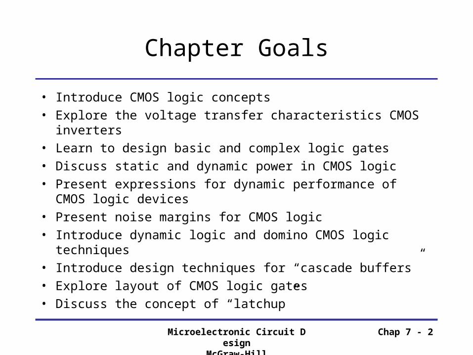
Chapter Goals
• Introduce CMOS logic concepts
• Explore the voltage transfer characteristics CMOS inverters
• Learn to design basic and complex logic gates
• Discuss static and dynamic power in CMOS logic
• Present expressions for dynamic performance of CMOS logic devices
• Present noise margins for CMOS logic
• Introduce dynamic logic and domino CMOS logic techniques
• Introduce design techniques for “cascade buffers”
• Explore layout of CMOS logic gates
• Discuss the concept of “latchup”
Microelectronic Circuit Design
McGraw-Hill
Chap 7 - 3
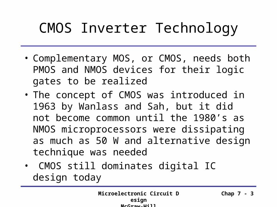
CMOS Inverter Technology
• Complementary MOS, or CMOS, needs both PMOS and NMOS devices for their logic gates to be realized
• The concept of CMOS was introduced in 1963 by Wanlass and Sah, but it did not become common until the 1980’s as NMOS microprocessors were dissipating as much as 50 W and alternative design technique was needed
• CMOS still dominates digital IC design today

Microelectronic Circuit Design
McGraw-Hill
Chap 7 - 4
CMOS Inverter Technology
• The CMOS inverter consists of a PMOS stacked on top on a NMOS, but they need to be fabricated on the same wafer
• To accomplish this, the technique of “n-well” implantation is needed as shown in the figure which shows the cross-section of a CMOS inverter
Microelectronic Circuit Design
McGraw-Hill
Chap 7 - 5
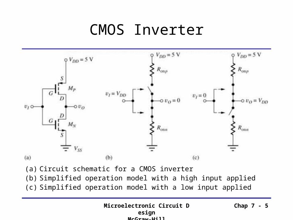
CMOS Inverter
(a) Circuit schematic for a CMOS inverter(b) Simplified operation model with a high input applied(c) Simplified operation model with a low input applied

Microelectronic Circuit Design
McGraw-Hill
Chap 7 - 6
CMOS Inverter Operation
• When vI is pulled high (VDD), the PMOS inverter is turned off, while the NMOS is turned on pulling the output down to VSS
• When vI is pulled low (VSS), the NMOS inverter is turned off, while the PMOS is turned on pulling the output up to VDD

Microelectronic Circuit Design
McGraw-Hill
Chap 7 - 7
CMOS Inverter Layout
• Two methods of laying out a CMOS inverter are shown
• The PMOS transistors lie within the n-well, whereas the NMOS transistors lie in the p-substrate
• Polysilicon is used to form common gate connections, and metal is used to tie the two drains together

Microelectronic Circuit Design
McGraw-Hill
Chap 7 - 8
Static Characteristics of the CMOS Inverter
• The figure shows the two modes of static operation with the circuit and simplified models
• Notice that VH = 5V and VL = 0V, and that ID
= 0A which means that there is no static power dissipation
Microelectronic Circuit Design
McGraw-Hill
Chap 7 - 9
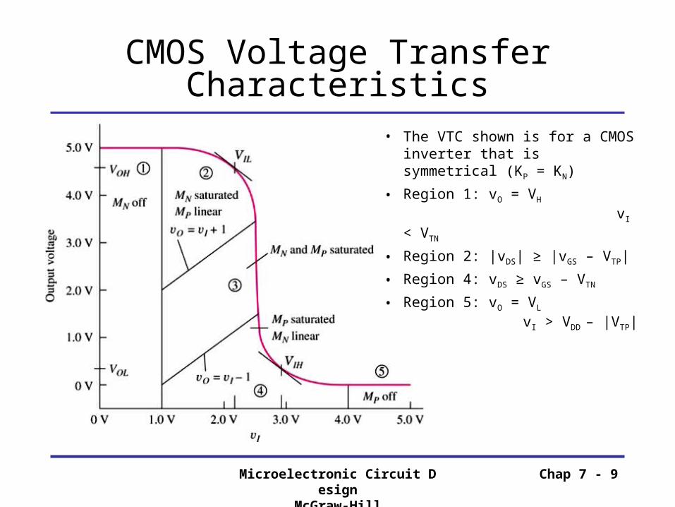
CMOS Voltage Transfer Characteristics
• The VTC shown is for a CMOS inverter that is symmetrical (KP = KN)
• Region 1: vO = VH
vI < VTN
• Region 2: |vDS| ≥ |vGS – VTP|
• Region 4: vDS ≥ vGS – VTN
• Region 5: vO = VL vI > VDD – |VTP|
Microelectronic Circuit Design
McGraw-Hill
Chap 7 - 10
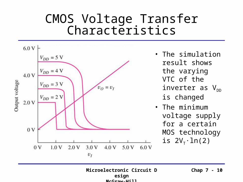
CMOS Voltage Transfer Characteristics
• The simulation result shows the varying VTC of the inverter as VDD is changed
• The minimum voltage supply for a certain MOS technology is 2VT∙ln(2)

Microelectronic Circuit Design
McGraw-Hill
Chap 7 - 11
CMOS Voltage Transfer Characteristics
• The simulation result shows the varying VTC of the inverter as KN/KP = KR is changed
• For KR > 1 the NMOS current drive is greater and it forces vI < VDD/2
• For KR < 1 the PMOS current drive is greater and it forces vI > VDD/2

Microelectronic Circuit Design
McGraw-Hill
Chap 7 - 12
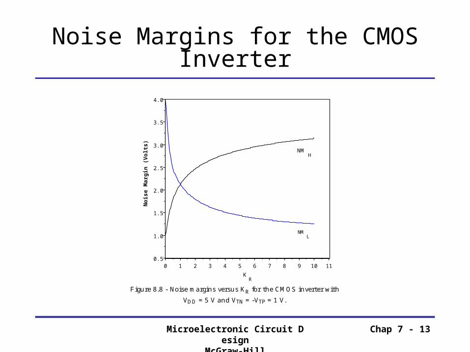
Noise Margins for the CMOS Inverter
• Noise margins are defined by the regions shown in the given figure
NML = VIL – VOL
NMH = VOH – VIH
Microelectronic Circuit Design
McGraw-Hill
Chap 7 - 13
Noise Margins for the CMOS Inverter
111098765432100.5
1.0
1.5
2.0
2.5
3.0
3.5
4.0
NM
NM
No
ise
Ma
rgin
(V
olt
s)
H
L
KR
Figure 8.8 - Noise margins versus KR for the CMOS inverter with
VDD = 5 V and VTN = -VTP = 1 V.
Microelectronic Circuit Design
McGraw-Hill
Chap 7 - 14
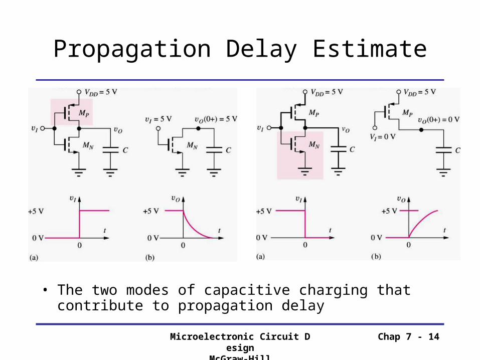
Propagation Delay Estimate
• The two modes of capacitive charging that contribute to propagation delay

Microelectronic Circuit Design
McGraw-Hill
Chap 7 - 15
Propagation Delay Estimate
• If it is assumed the inverter in “symmetrical”, (W/L)P = 2.5(W/L)N, then τPLH = τPHL
PHLPLHPHL
p
TNHnonN
TNH
TN
LH
TNHonNPHL
VVKR
VV
V
VV
VVCR
2
1
214ln

Microelectronic Circuit Design
McGraw-Hill
Chap 7 - 16
Rise and Fall Times
• The rise and fall times are given by the following expressions:
PLHr
PHLf
t
t
2
2
Microelectronic Circuit Design
McGraw-Hill
Chap 7 - 17
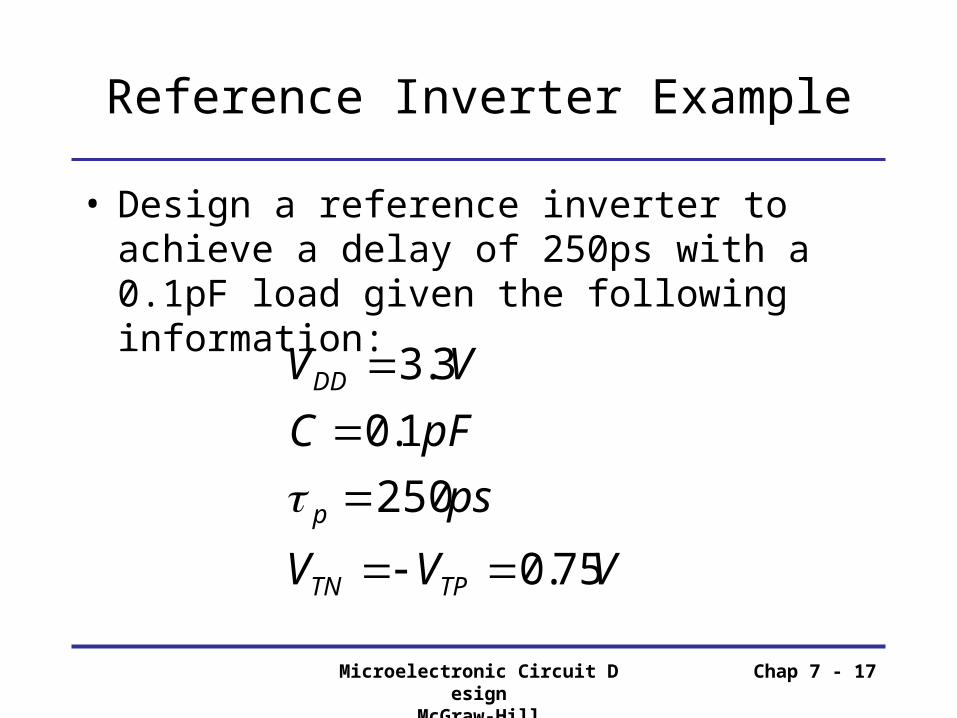
Reference Inverter Example
• Design a reference inverter to achieve a delay of 250ps with a 0.1pF load given the following information:
VVV
ps
pFC
VV
TPTN
p
DD
75.0
250
1.0
3.3

Microelectronic Circuit Design
McGraw-Hill
Chap 7 - 18
Reference Inverter Example
• Assuming the inverter is symmetrical and using the values given in Table 7.1:
psV
AK
V
AK
PLHPHLp
p
n
250
10
25
2'
2'
Microelectronic Circuit Design
McGraw-Hill
Chap 7 - 19
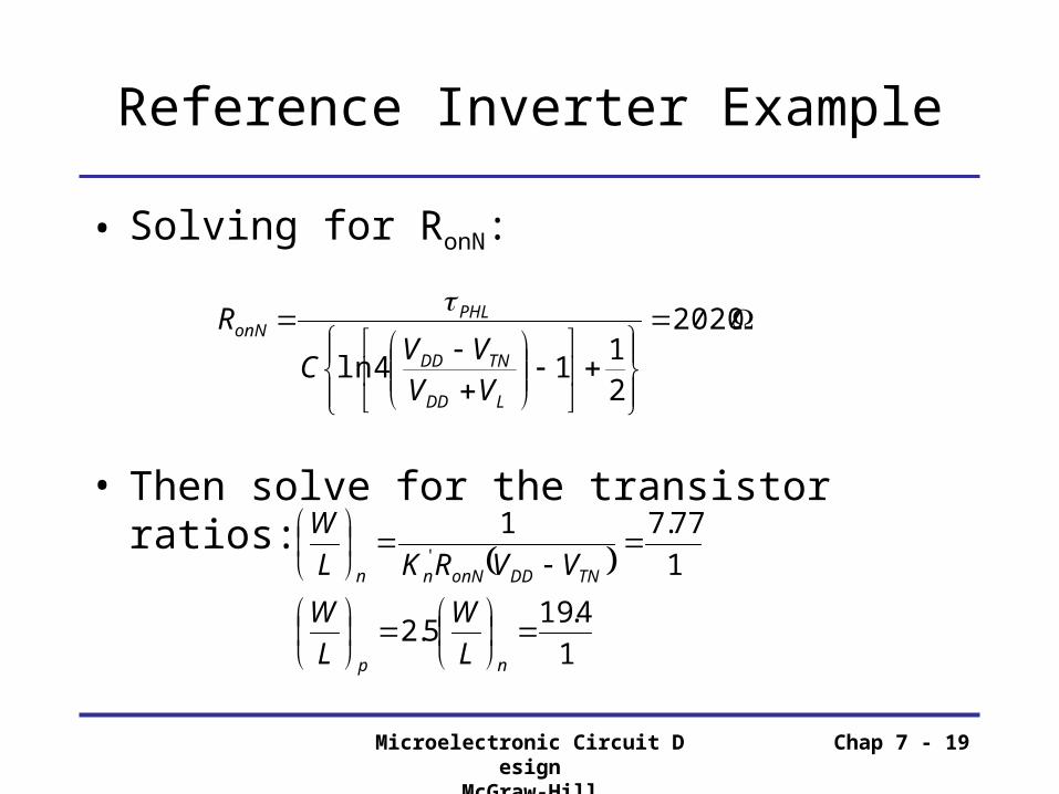
Reference Inverter Example
• Solving for RonN:
• Then solve for the transistor ratios:
2020
21
14lnLDD
TNDD
PHLonN
VV
VVC
R
1
4.195.2
1
77.71'
np
TNDDonNnn
L
W
L
W
VVRKL
W

Microelectronic Circuit Design
McGraw-Hill
Chap 7 - 20
Delay of Cascaded Inverters
• An ideal step was used to derive the previous delay equations, but this is not possible to implement
• By putting the following circuit in SPICE, it is possible to produce more accurate equations
Microelectronic Circuit Design
McGraw-Hill
Chap 7 - 21
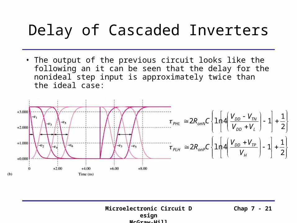
Delay of Cascaded Inverters
• The output of the previous circuit looks like the following an it can be seen that the delay for the nonideal step input is approximately twice than the ideal case:
2
114ln2
2
114ln2
H
TPDDonPPLH
LDD
TNDDonNPHL
V
VVCR
VV
VVCR
Microelectronic Circuit Design
McGraw-Hill
Chap 7 - 22
Static Power Dissipation
• CMOS logic is considered to have no static power dissipation
• Since the ROFF of the two transistors is very large, the DC current driving a capacitive load is zero
• This is not completely accurate since MOS transistors have leakage currents associated with the reverse-biased drain-to-substrate connections
Microelectronic Circuit Design
McGraw-Hill
Chap 7 - 23
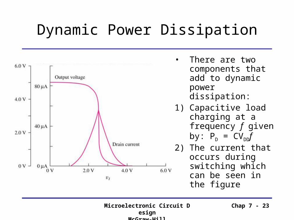
Dynamic Power Dissipation
• There are two components that add to dynamic power dissipation:
1) Capacitive load charging at a frequency f given by: PD = CVDDf
2) The current that occurs during switching which can be seen in the figure
Microelectronic Circuit Design
McGraw-Hill
Chap 7 - 24
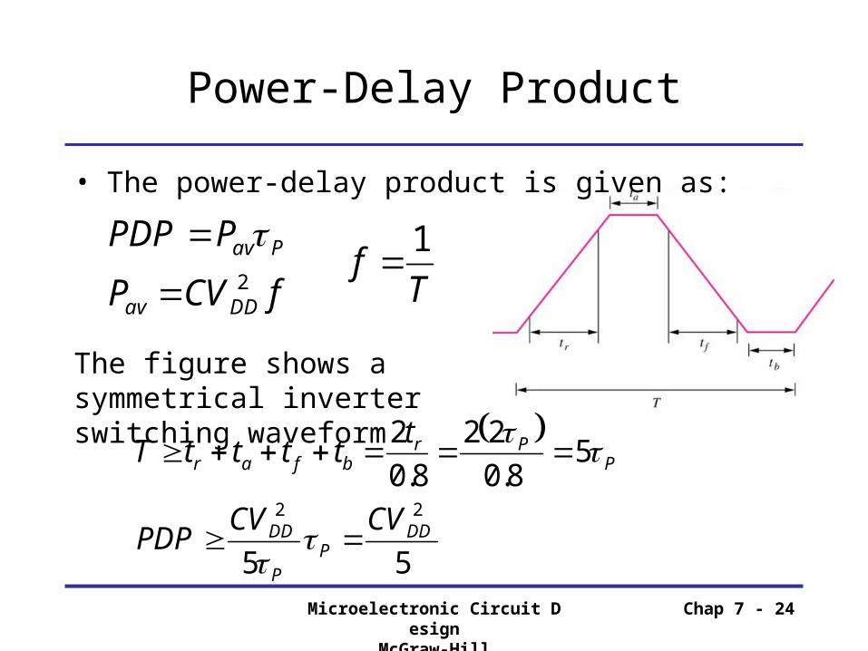
Power-Delay Product
fCVP
PPDP
DDav
Pav
2
The figure shows a symmetrical inverter switching waveform
Tf
1
55
58.0
22
8.0
2
22DD
PP
DD
PPr
bfar
CVCVPDP
tttttT
• The power-delay product is given as:
Microelectronic Circuit Design
McGraw-Hill
Chap 7 - 25
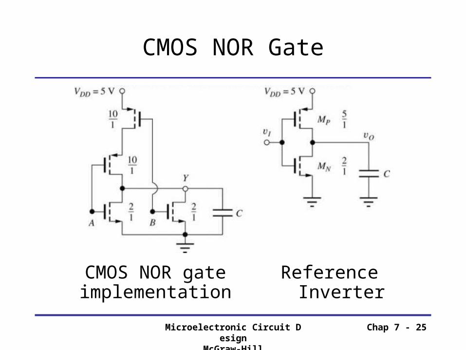
CMOS NOR Gate
Reference InverterCMOS NOR gate implementation
Microelectronic Circuit Design
McGraw-Hill
Chap 7 - 26
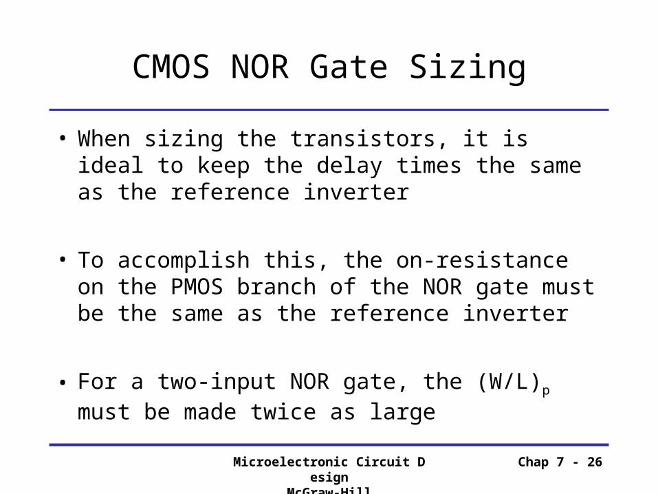
CMOS NOR Gate Sizing
• When sizing the transistors, it is ideal to keep the delay times the same as the reference inverter
• To accomplish this, the on-resistance on the PMOS branch of the NOR gate must be the same as the reference inverter
• For a two-input NOR gate, the (W/L)p must be made twice as large

Microelectronic Circuit Design
McGraw-Hill
Chap 7 - 27
CMOS NOR Gate Body Effect
• Since the bottom PMOS body contact is not connected to its source, its threshold voltage changes as VSB changes during switching
• Once vO = VH is reached, the bottom PMOS is not affected by body effect, thus the total on-resistance of the PMOS branch is the same
• However, the rise time is slowed down due to |VTP| being a function of time
Microelectronic Circuit Design
McGraw-Hill
Chap 7 - 28
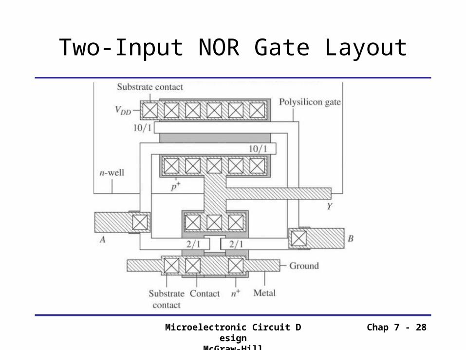
Two-Input NOR Gate Layout
Microelectronic Circuit Design
McGraw-Hill
Chap 7 - 29
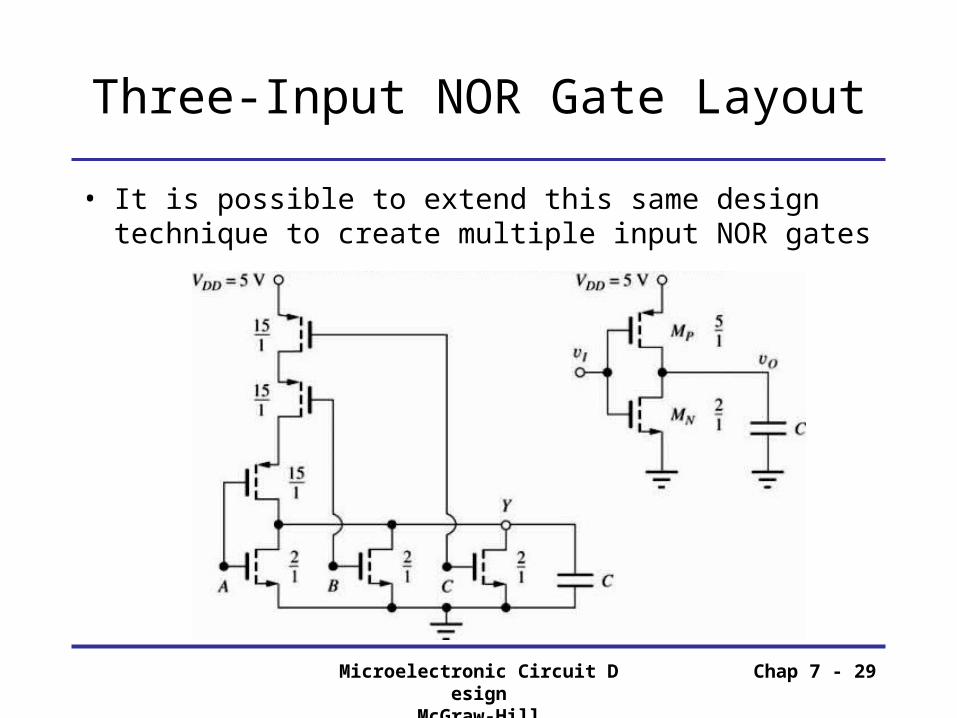
Three-Input NOR Gate Layout
• It is possible to extend this same design technique to create multiple input NOR gates
Microelectronic Circuit Design
McGraw-Hill
Chap 7 - 30
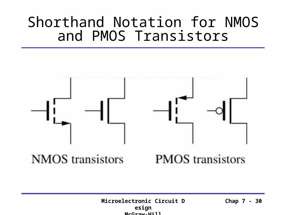
Shorthand Notation for NMOS and PMOS Transistors
Microelectronic Circuit Design
McGraw-Hill
Chap 7 - 31
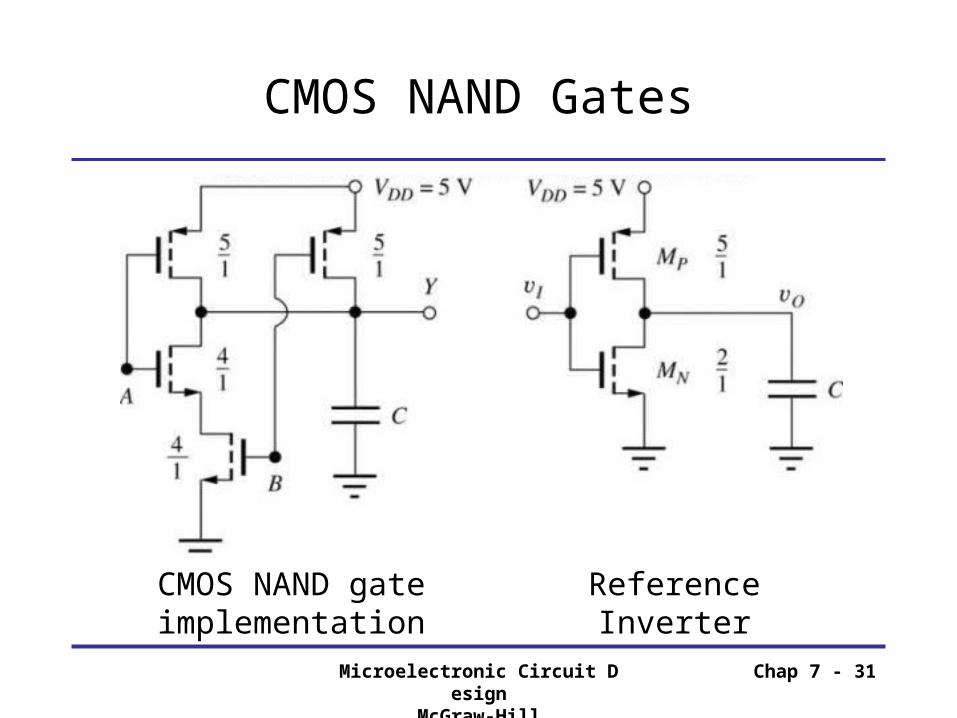
CMOS NAND Gates
CMOS NAND gate implementation
Reference Inverter
Microelectronic Circuit Design
McGraw-Hill
Chap 7 - 32
CMOS NAND Gates Sizing
• The same rules apply for sizing the NAND gate as the did for the NOR gate, except for now the NMOS transistors are in series
• The (W/L)N will be twice the size of the reference inverter’s NMOS

Microelectronic Circuit Design
McGraw-Hill
Chap 7 - 33
Multi-Input CMOS NAND Gates
Microelectronic Circuit Design
McGraw-Hill
Chap 7 - 34
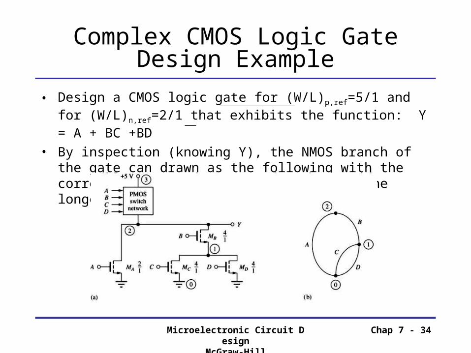
Complex CMOS Logic Gate Design Example
• Design a CMOS logic gate for (W/L)p,ref=5/1 and for (W/L)n,ref=2/1 that exhibits the function: Y = A + BC +BD
• By inspection (knowing Y), the NMOS branch of the gate can drawn as the following with the corresponding graph, while considering the longest path for sizing purposes:
Microelectronic Circuit Design
McGraw-Hill
Chap 7 - 35
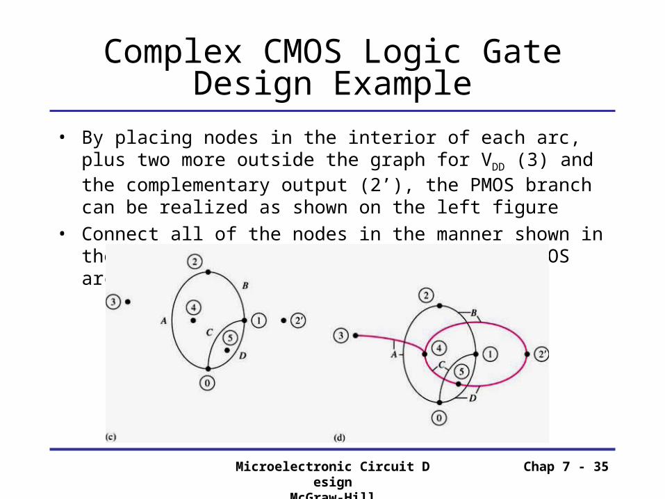
Complex CMOS Logic Gate Design Example
• By placing nodes in the interior of each arc, plus two more outside the graph for VDD (3) and the complementary output (2’), the PMOS branch can be realized as shown on the left figure
• Connect all of the nodes in the manner shown in the right figure, and the NMOS arc that PMOS arc intersects have the same inputs

Microelectronic Circuit Design
McGraw-Hill
Chap 7 - 36
Complex CMOS Logic Gate Design Example
• From the PMOS graph, the PMOS branch can now be drawn for the final CMOS logic gate while once again considering the longest PMOS path for sizing

Microelectronic Circuit Design
McGraw-Hill
Chap 7 - 37
Complex CMOS Gate with a Bridging Transistor Design Example
• Design a CMOS gate that implements the following logic function using the same reference inverter sizes as the previous example: Y = AB +CE + ADE + CDB
• The NMOS branch can be realized in the following manner using bridging NMOS D to implement Y. The corresponding NMOS graph is shown to the right.

Microelectronic Circuit Design
McGraw-Hill
Chap 7 - 38
Complex CMOS Gate with a Bridging Transistor Design Example
• By using the same technique as before, the PMOS graph can now be drawn

Microelectronic Circuit Design
McGraw-Hill
Chap 7 - 39
Complex CMOS Gate with a Bridging Transistor Design Example
• By using the PMOS graph the PMOS branch can now be realized as the following (considering the longest path for sizing)

Microelectronic Circuit Design
McGraw-Hill
Chap 7 - 40
Minimum Size Gate Design and Performance
• With CMOS technology, there is a area/delay tradeoff that needs to be considered
• If minimum feature sized are used for both devices, then the τPLH will be decreased compared to the symmetrical reference inverter

Microelectronic Circuit Design
McGraw-Hill
Chap 7 - 41
Minimum Size Complex Gate and Layout
• The following shows the layout of a complex minimum size logic gate
Microelectronic Circuit Design
McGraw-Hill
Chap 7 - 46
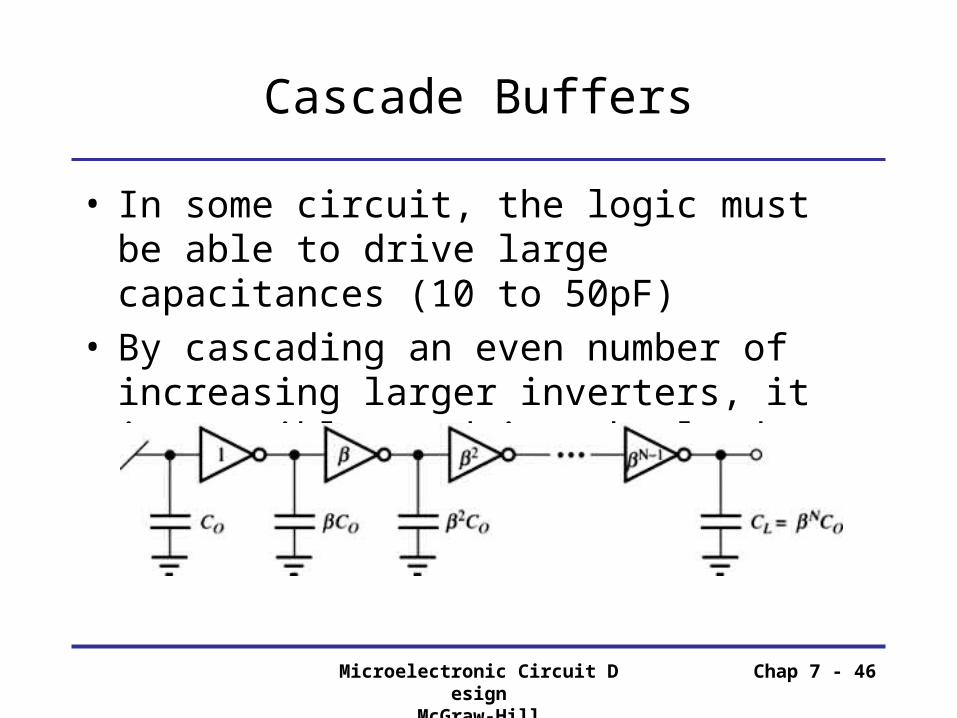
Cascade Buffers
• In some circuit, the logic must be able to drive large capacitances (10 to 50pF)
• By cascading an even number of increasing larger inverters, it is possible to drive the loads

Microelectronic Circuit Design
McGraw-Hill
Chap 7 - 47
Cascade Buffers
• The taper factor β determines the increase of the cascaded inverter’s size in manner shown of the previous image.
where Co is the unit inverter’s load capacitance
• The delay of the cascaded buffer is given by the following:
o
LN
C
C
o
N
o
LB C
CN
/1
Where τo is the unit inverter’s
propagation delay

Microelectronic Circuit Design
McGraw-Hill
Chap 7 - 48
Optimum Design of Cascaded Stages
• The following expressions can aid in the design of an optimum cascaded buffer
oo
LBopt
C
C
o
Lopt
o
Lopt
C
C
C
C
C
CN
o
L
ln
ln
ln
1

Microelectronic Circuit Design
McGraw-Hill
Chap 7 - 49
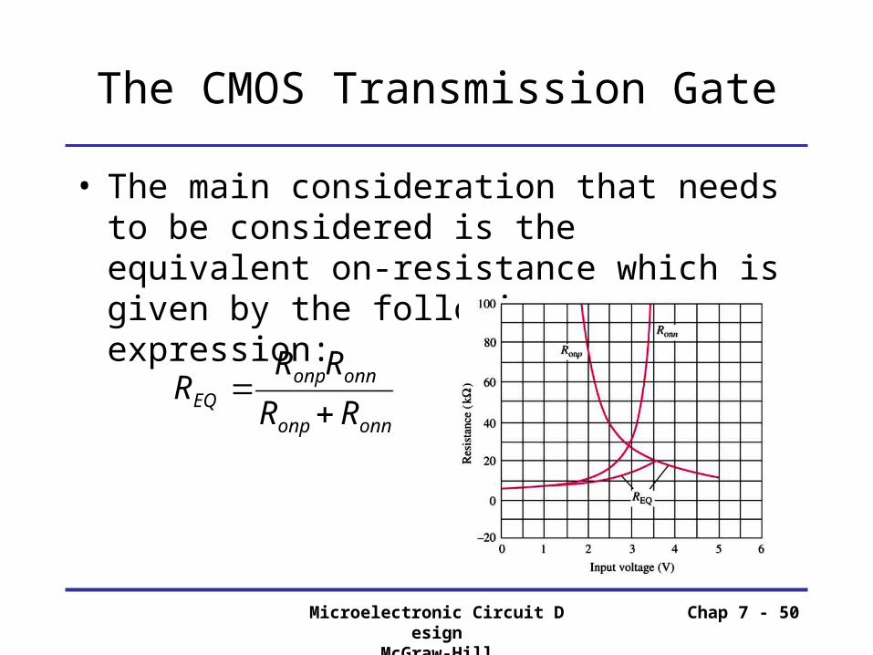
The CMOS Transmission Gate
• The CMOS transmission gate (T-gate) is one of the most useful circuits for both analog and digital applications
• It acts as a switch that can operate up to VDD and down to VSS
Microelectronic Circuit Design
McGraw-Hill
Chap 7 - 50
The CMOS Transmission Gate
• The main consideration that needs to be considered is the equivalent on-resistance which is given by the following expression:
onnonp
onnonpEQ RR
RRR
Microelectronic Circuit Design
McGraw-Hill
Chap 7 - 51
CMOS Latchup
• There is one major downfall to the CMOS logic gate – Latchup
• There are many safeguards that are done during fabrication to suppress this, but it can still occur under certain transient or fault conditions
Microelectronic Circuit Design
McGraw-Hill
Chap 7 - 52
CMOS Latchup
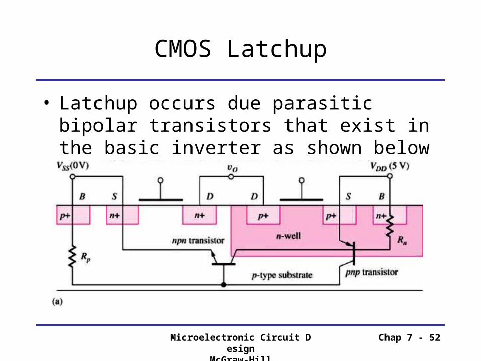
• Latchup occurs due parasitic bipolar transistors that exist in the basic inverter as shown below
Microelectronic Circuit Design
McGraw-Hill
Chap 7 - 53
CMOS Latchup
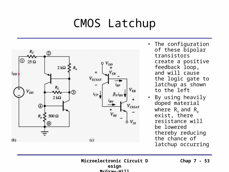
• The configuration of these bipolar transistors create a positive feedback loop, and will cause the logic gate to latchup as shown to the left
• By using heavily doped material where Rn and Rp exist, there resistance will be lowered thereby reducing the chance of latchup occurring
Microelectronic Circuit Design
McGraw-Hill
Chap 7 - 54
CMOS Latchup
• Suppose a base current iBN begins to flow in the base of the npn transistor. This base current is amplified by the npn current gain N an must be supplied from the base of the pnp transistor. The pnp base current is then amplified further by the current gain P of the pnp transistor, yielding a collector current equal to
• iCP = PiBP = P(NiBN) (8.26)

Microelectronic Circuit Design
McGraw-Hill
Chap 7 - 55
CMOS Latchup
• Once the circuit has entered the latchup state, both transistors saturate, and the voltage across the structure collapses to one diode drop plus one saturation voltage.
• V = VEB+VCESAT = VBE + VECSAT (8.27)• After latch up happened, the current increases to (VDD-
0.8)/RC. The current level is only limited by the external circuit components.
• Large currents and power dissipation can rapidly destroy most CMOS structures. e.g. electro-migration will damage the metal lines.
Microelectronic Circuit Design
McGraw-Hill
Chap 7 - 56
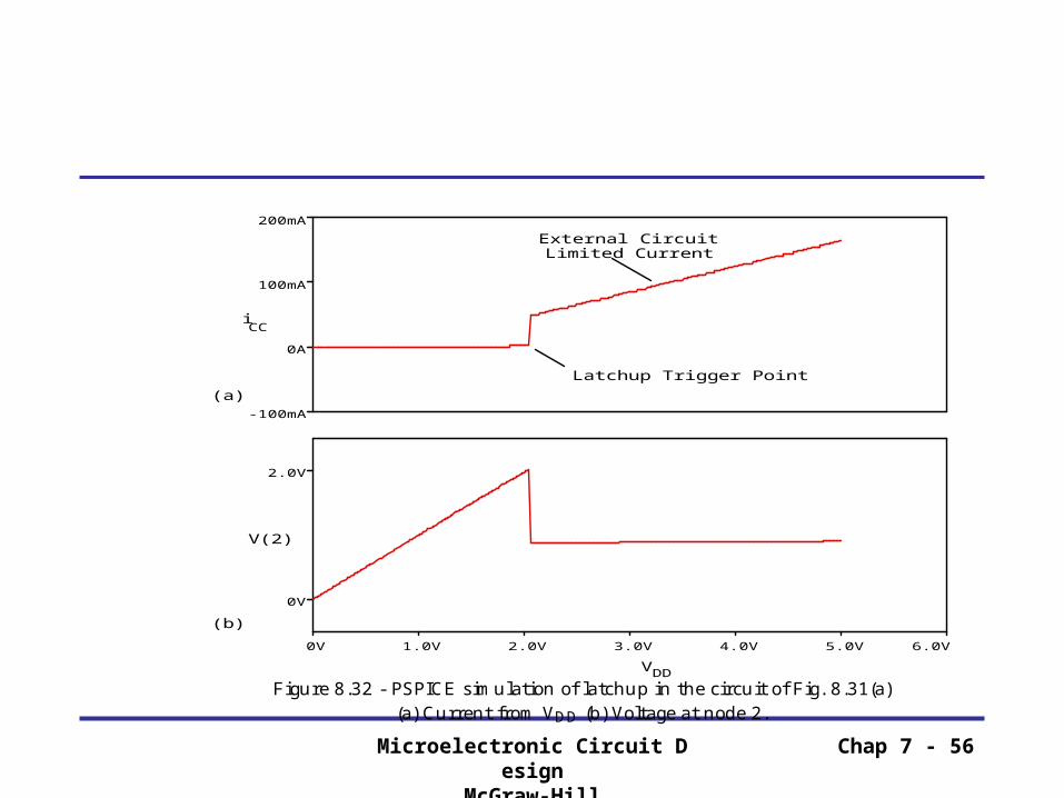
0V 1.0V 2.0V 3.0V 4.0V 5.0V 6.0V
2.0V
0V
V(2)
200mA
100mA
0A
-100mA
Limited CurrentExternal Circuit
Latchup Trigger Point
(a)
(b)
DDV
iCC
Figure 8.32 - PSPICE simulation of latchup in the circuit of Fig. 8.31(a) (a) Current from VDD (b) Voltage at node 2.
Microelectronic Circuit Design
McGraw-Hill
Chap 7 - 57
CMOS Latchup
• Latchup would not occur in an ideal structure for which Rn = 0 = Rp – modern CMOS technology uses special substrates and processing to minimize the values of these two resistors.
• A fault or transient occurs that causes one of the source or drain diffusions to momentarily exceed the power supply voltage levels, the latchup can be triggered.
• Ionizing radiation or intense optical illumination are two other possible sources of latchup initiation.
Microelectronic Circuit Design
McGraw-Hill
Chap 7 - 58
Latch-up Prevention
Latchup resistant CMOS processes – reduce the gain the the parasitic transistors.Layout techniques - Use substrate contact to
reduce Rn & Rp.

Microelectronic Circuit Design
McGraw-Hill
Chap 7 - 59
Homework
7.32
7.61
7.71

Microelectronic Circuit Design
McGraw-Hill
Chap 7 - 60
Additional CMOS Design Issues
Power EconomySizing Routing ConductorsDesign MarginingYieldReliability

Microelectronic Circuit Design
McGraw-Hill
Chap 7 - 61
Power Economy
In large projects, each module is usually given a power budget. It is then the designer’s job to meet this constraint (in addition to all the other normal constrains).DC Power dissipation is reduced to leakage by
using CMOS logic gates.Leakage is proportional to the area of diffusion, so
use minimum-sized device if possible.
Microelectronic Circuit Design
McGraw-Hill
Chap 7 - 62
Power Economy (cont.)
Dynamic Power Dissipation may be limited by reducing supply voltage, switched capacitance, and the clock frequency.Capacitance can be minimized by optimal
placement and routing.Only operate minimum amount of logic at high
speed.Having a variable clock depending on how much
computation has to be completed.

Microelectronic Circuit Design
McGraw-Hill
Chap 7 - 63
Sizing Routing Conductors
Electromigration – determine the minimum width of conductors
Power supply noise and integrity – need to maintain VDD and VSS levels
RC delay – for speed reasonPower and Ground Bounce : due to current draw change.
Happens in clock transition, or I/O pads. Often large on-chip “bypass” capacitors are added to minimize its effect.
Contact Replication
Microelectronic Circuit Design
McGraw-Hill
Chap 7 - 64
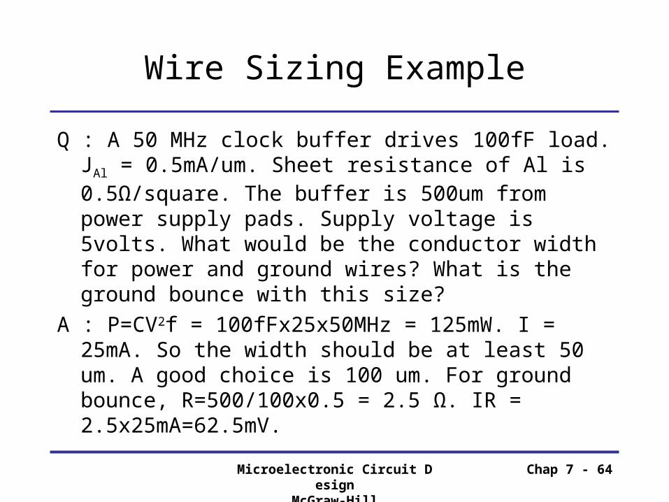
Wire Sizing Example
Q : A 50 MHz clock buffer drives 100fF load. JAl = 0.5mA/um. Sheet resistance of Al is 0.5Ω/square. The buffer is 500um from power supply pads. Supply voltage is 5volts. What would be the conductor width for power and ground wires? What is the ground bounce with this size?
A : P=CV2f = 100fFx25x50MHz = 125mW. I = 25mA. So the width should be at least 50 um. A good choice is 100 um. For ground bounce, R=500/100x0.5 = 2.5 Ω. IR = 2.5x25mA=62.5mV.
Microelectronic Circuit Design
McGraw-Hill
Chap 7 - 65
Design Margining
Operating temperature : ambient temperature range : 0 to 70 °C. Commercial parts: -40°C to 85°C. Military parts: -55 °C to 125 °C.Supply Voltage: +/-10% of the supply voltage.Process Variation

Microelectronic Circuit Design
McGraw-Hill
Chap 7 - 66
Process Variation
The fabrication process is a long sequence of chemical reactions that result in device characteristics that follow a normal or Gaussian distribution. Retaining parts with a 3σdistribution will result
in .26% rejection rate. 2σresults in 4.56%, while 1σresults in 31.74%. Boundary cases of transistors are described by :
nominal, fast and slow.
Microelectronic Circuit Design
McGraw-Hill
Chap 7 - 67
Design Corners
High-Speed/Worst-Power Corner: fast-n/fast-p, high supply voltage and lowest temperature. Determines the package. Also check for setup and hold time constraints.
Worst-Speed Corner: slow-n/slow-p, low supply voltage and highest temperature. Determines the chip operational frequency. Good safe design gives 10 to 20% speed for margin.
Other corners must also be checked to ensure memory, analog circuit, ratioed logic works properly.
Microelectronic Circuit Design
McGraw-Hill
Chap 7 - 68
Packaging Issues
When choose package need to consider pin count, power dissipation, cost.Heat sink can be added to relief power dissipation
requirements, at the cost of additional cost and space requirement.Need to consider lead inductance for speed reason.

Microelectronic Circuit Design
McGraw-Hill
Chap 7 - 69
Package Types Examples 1

Microelectronic Circuit Design
McGraw-Hill
Chap 7 - 70
Package Types Examples 2

Microelectronic Circuit Design
McGraw-Hill
Chap 7 - 71
Package Types Examples 3
Microelectronic Circuit Design
McGraw-Hill
Chap 7 - 72
Yield
Yield is defined as the ratio between known good chip on wafer and total number of chips on wafer.Yield is a function of chip area and defect density.

Microelectronic Circuit Design
McGraw-Hill
Chap 7 - 73
Reliability
Hot Electron effectsElectromigrationOxide failureBipolar transistor degradationPackage/Chip power dissipation (die temperature)ESD(electrostatic discharge) protection

Microelectronic Circuit Design
McGraw-Hill
Chap 7 - 74
What are the jobs in a IC design company?
CEO CTO Marketing Architect Chip Lead Front-end (Digital Logic Designer) Synthesis Engineer Verification Engineer Analog Designer Back-end (Physical Design) CAD Tool Support System Engineer Software Engineer Test Engineer
Microelectronic Circuit Design
McGraw-Hill
Chap 7 - 75
IC Market Space (3C’s)
Computer – Intel, IBM, ATI, nVidia, Via• CPU (PC, Server, Workstation, Mainframe)
• Graphic Accelerator
• Chip Set (for PC,Server, …)
Communication – Motorola, Broadcom• Wireless (Cellular phone, WLAN)
• Wired (LAN, Fiber backbone)
Consumer – ManyTV, Car, MP3, Toys, Game, …..
Microelectronic Circuit Design
McGraw-Hill
Chap 7 - 76
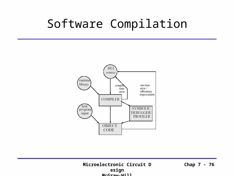
Software Compilation
Microelectronic Circuit Design
McGraw-Hill
Chap 7 - 77
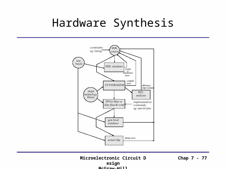
Hardware Synthesis

Microelectronic Circuit Design
McGraw-Hill
Chap 7 - 78
Modern SoC Design Flow
Market Definition / Customer SpecificationSystem DesignHardware Architecture DesignRTL DevelopmentVerificationSynthesisPhysical LayoutSystem Qualification
Microelectronic Circuit Design
McGraw-Hill
Chap 7 - 79
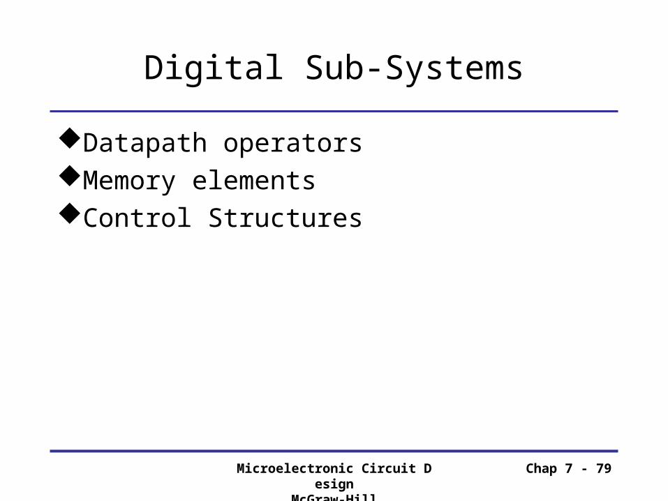
Digital Sub-Systems
Datapath operatorsMemory elementsControl Structures

Microelectronic Circuit Design
McGraw-Hill
Chap 7 - 80
Datapath operators
Datapath operators form a important subclass of VLSI circuit design. N-bit data is generally processed, which naturally leads to the ability to use n identical circuits to implement the function.
Generally, data may be arranged to flow in one direction, while any control signals are introduced in an orthogonal direction to the dataflow.

Microelectronic Circuit Design
McGraw-Hill
Chap 7 - 81
Datapath Operator Examples
Addition/SubtractionComparatorsBinary CountersBoolean Operations – ALUsMultiplicationShifter

Microelectronic Circuit Design
McGraw-Hill
Chap 7 - 82
Microelectronic Circuit Design
McGraw-Hill
Chap 7 - 83
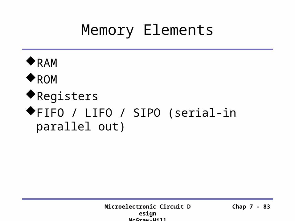
Memory Elements
RAMROMRegistersFIFO / LIFO / SIPO (serial-in parallel out)

Microelectronic Circuit Design
McGraw-Hill
Chap 7 - 84
Microelectronic Circuit Design
McGraw-Hill
Chap 7 - 85
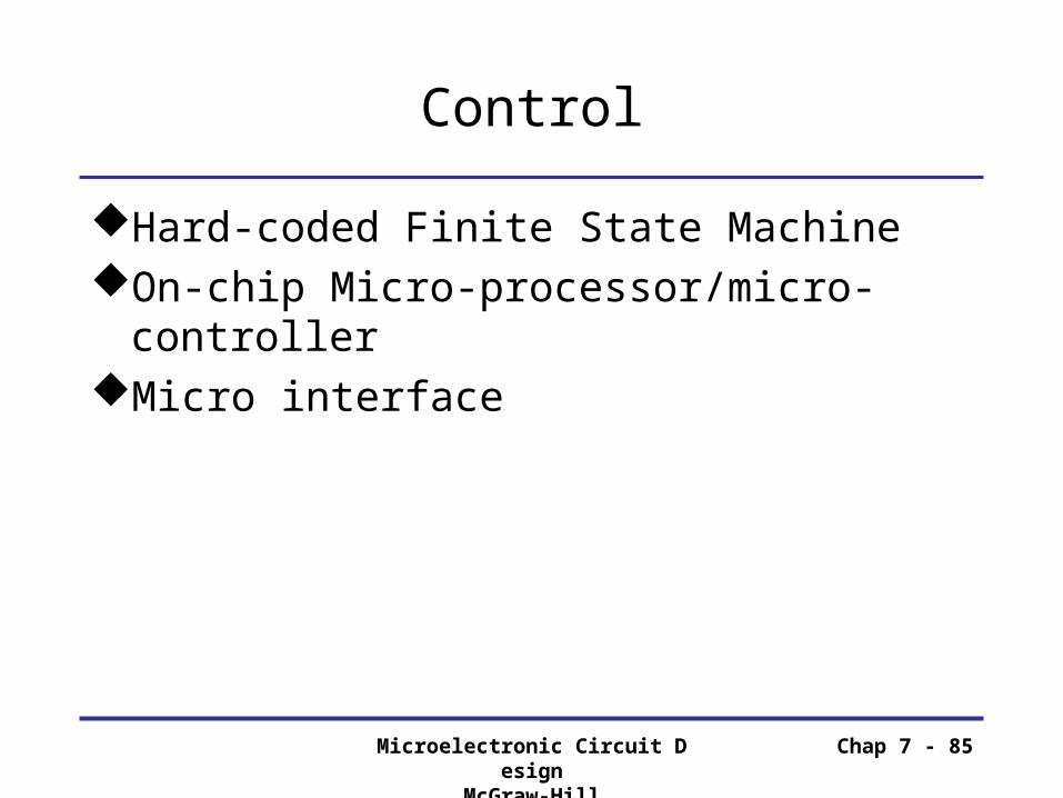
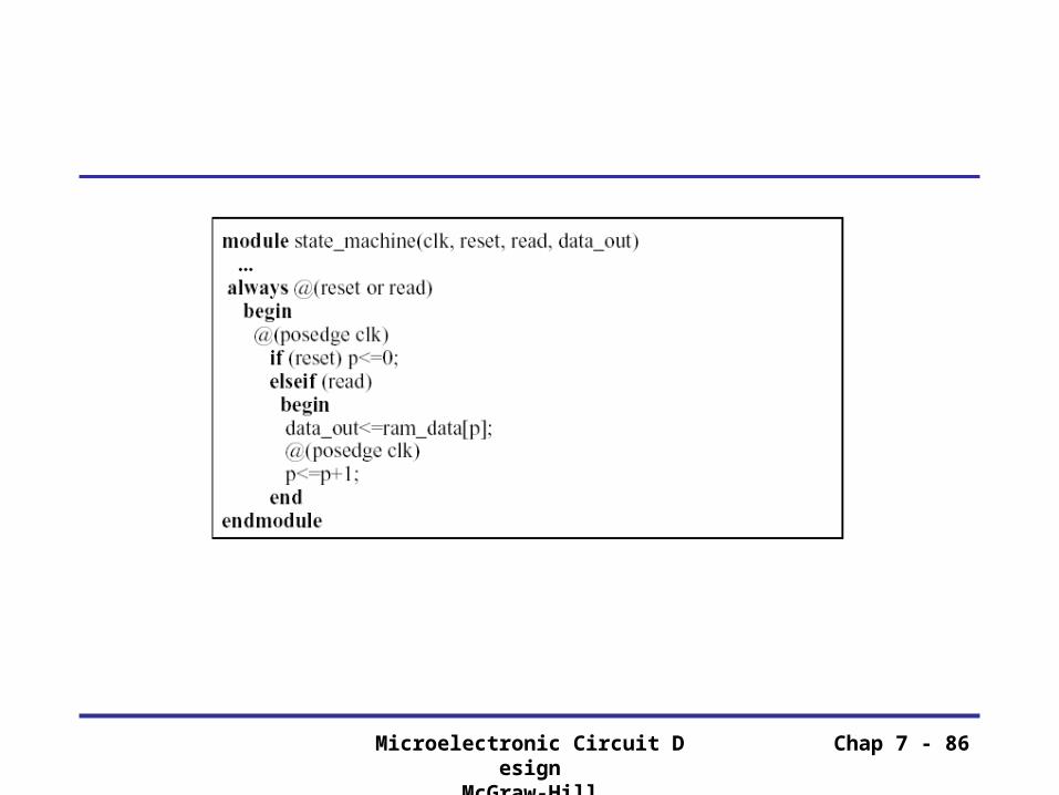
Control
Hard-coded Finite State MachineOn-chip Micro-processor/micro-controllerMicro interface
Microelectronic Circuit Design
McGraw-Hill
Chap 7 - 86
Microelectronic Circuit Design
McGraw-Hill
Chap 7 - 87
End of Chapter 7


